JP2019004030A - 半導体装置 - Google Patents
半導体装置 Download PDFInfo
- Publication number
- JP2019004030A JP2019004030A JP2017117072A JP2017117072A JP2019004030A JP 2019004030 A JP2019004030 A JP 2019004030A JP 2017117072 A JP2017117072 A JP 2017117072A JP 2017117072 A JP2017117072 A JP 2017117072A JP 2019004030 A JP2019004030 A JP 2019004030A
- Authority
- JP
- Japan
- Prior art keywords
- layer
- collector
- region
- drift
- semiconductor substrate
- Prior art date
- Legal status (The legal status is an assumption and is not a legal conclusion. Google has not performed a legal analysis and makes no representation as to the accuracy of the status listed.)
- Pending
Links
- 239000004065 semiconductor Substances 0.000 title claims abstract description 85
- 239000000758 substrate Substances 0.000 claims abstract description 50
- 238000011084 recovery Methods 0.000 claims abstract description 24
- 239000010410 layer Substances 0.000 claims description 273
- 239000012535 impurity Substances 0.000 claims description 12
- 238000002347 injection Methods 0.000 claims description 10
- 239000007924 injection Substances 0.000 claims description 10
- 239000002344 surface layer Substances 0.000 claims description 6
- 239000000969 carrier Substances 0.000 description 4
- 239000011229 interlayer Substances 0.000 description 4
- 230000007423 decrease Effects 0.000 description 3
- XUIMIQQOPSSXEZ-UHFFFAOYSA-N Silicon Chemical compound [Si] XUIMIQQOPSSXEZ-UHFFFAOYSA-N 0.000 description 2
- 229910052710 silicon Inorganic materials 0.000 description 2
- 239000010703 silicon Substances 0.000 description 2
- 238000004088 simulation Methods 0.000 description 2
- ZOXJGFHDIHLPTG-UHFFFAOYSA-N Boron Chemical compound [B] ZOXJGFHDIHLPTG-UHFFFAOYSA-N 0.000 description 1
- 229910052796 boron Inorganic materials 0.000 description 1
- 238000010586 diagram Methods 0.000 description 1
- 239000011521 glass Substances 0.000 description 1
- BHEPBYXIRTUNPN-UHFFFAOYSA-N hydridophosphorus(.) (triplet) Chemical compound [PH] BHEPBYXIRTUNPN-UHFFFAOYSA-N 0.000 description 1
- 229910021420 polycrystalline silicon Inorganic materials 0.000 description 1
- 229920005591 polysilicon Polymers 0.000 description 1
Images


Classifications
-
- H—ELECTRICITY
- H01—ELECTRIC ELEMENTS
- H01L—SEMICONDUCTOR DEVICES NOT COVERED BY CLASS H10
- H01L21/00—Processes or apparatus adapted for the manufacture or treatment of semiconductor or solid state devices or of parts thereof
- H01L21/70—Manufacture or treatment of devices consisting of a plurality of solid state components formed in or on a common substrate or of parts thereof; Manufacture of integrated circuit devices or of parts thereof
- H01L21/77—Manufacture or treatment of devices consisting of a plurality of solid state components or integrated circuits formed in, or on, a common substrate
- H01L21/78—Manufacture or treatment of devices consisting of a plurality of solid state components or integrated circuits formed in, or on, a common substrate with subsequent division of the substrate into plural individual devices
- H01L21/82—Manufacture or treatment of devices consisting of a plurality of solid state components or integrated circuits formed in, or on, a common substrate with subsequent division of the substrate into plural individual devices to produce devices, e.g. integrated circuits, each consisting of a plurality of components
- H01L21/822—Manufacture or treatment of devices consisting of a plurality of solid state components or integrated circuits formed in, or on, a common substrate with subsequent division of the substrate into plural individual devices to produce devices, e.g. integrated circuits, each consisting of a plurality of components the substrate being a semiconductor, using silicon technology
- H01L21/8232—Field-effect technology
- H01L21/8234—MIS technology, i.e. integration processes of field effect transistors of the conductor-insulator-semiconductor type
-
- H—ELECTRICITY
- H01—ELECTRIC ELEMENTS
- H01L—SEMICONDUCTOR DEVICES NOT COVERED BY CLASS H10
- H01L27/00—Devices consisting of a plurality of semiconductor or other solid-state components formed in or on a common substrate
- H01L27/02—Devices consisting of a plurality of semiconductor or other solid-state components formed in or on a common substrate including semiconductor components specially adapted for rectifying, oscillating, amplifying or switching and having at least one potential-jump barrier or surface barrier; including integrated passive circuit elements with at least one potential-jump barrier or surface barrier
- H01L27/04—Devices consisting of a plurality of semiconductor or other solid-state components formed in or on a common substrate including semiconductor components specially adapted for rectifying, oscillating, amplifying or switching and having at least one potential-jump barrier or surface barrier; including integrated passive circuit elements with at least one potential-jump barrier or surface barrier the substrate being a semiconductor body
- H01L27/06—Devices consisting of a plurality of semiconductor or other solid-state components formed in or on a common substrate including semiconductor components specially adapted for rectifying, oscillating, amplifying or switching and having at least one potential-jump barrier or surface barrier; including integrated passive circuit elements with at least one potential-jump barrier or surface barrier the substrate being a semiconductor body including a plurality of individual components in a non-repetitive configuration
-
- H—ELECTRICITY
- H01—ELECTRIC ELEMENTS
- H01L—SEMICONDUCTOR DEVICES NOT COVERED BY CLASS H10
- H01L29/00—Semiconductor devices adapted for rectifying, amplifying, oscillating or switching, or capacitors or resistors with at least one potential-jump barrier or surface barrier, e.g. PN junction depletion layer or carrier concentration layer; Details of semiconductor bodies or of electrodes thereof ; Multistep manufacturing processes therefor
- H01L29/66—Types of semiconductor device ; Multistep manufacturing processes therefor
- H01L29/68—Types of semiconductor device ; Multistep manufacturing processes therefor controllable by only the electric current supplied, or only the electric potential applied, to an electrode which does not carry the current to be rectified, amplified or switched
- H01L29/70—Bipolar devices
- H01L29/72—Transistor-type devices, i.e. able to continuously respond to applied control signals
- H01L29/739—Transistor-type devices, i.e. able to continuously respond to applied control signals controlled by field-effect, e.g. bipolar static induction transistors [BSIT]
-
- H—ELECTRICITY
- H01—ELECTRIC ELEMENTS
- H01L—SEMICONDUCTOR DEVICES NOT COVERED BY CLASS H10
- H01L29/00—Semiconductor devices adapted for rectifying, amplifying, oscillating or switching, or capacitors or resistors with at least one potential-jump barrier or surface barrier, e.g. PN junction depletion layer or carrier concentration layer; Details of semiconductor bodies or of electrodes thereof ; Multistep manufacturing processes therefor
- H01L29/66—Types of semiconductor device ; Multistep manufacturing processes therefor
- H01L29/68—Types of semiconductor device ; Multistep manufacturing processes therefor controllable by only the electric current supplied, or only the electric potential applied, to an electrode which does not carry the current to be rectified, amplified or switched
- H01L29/76—Unipolar devices, e.g. field effect transistors
- H01L29/772—Field effect transistors
- H01L29/78—Field effect transistors with field effect produced by an insulated gate
Abstract
Description
第1実施形態について図面を参照しつつ説明する。なお、本実施形態の半導体装置は、例えば、インバータ、DC/DCコンバータ等の電源回路に使用されるパワースイッチング素子として利用されると好適である。
第2実施形態について説明する。第2実施形態は、第1実施形態に対して、カソード層21内にキャリア注入層を形成したものであり、その他に関しては第1実施形態と同様であるため、ここでは説明を省略する。
本発明は上記した実施形態に限定されるものではなく、特許請求の範囲に記載した範囲内において適宜変更が可能である。
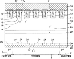
1a IGBT素子
2 FWD領域
2a FWD素子
10 半導体基板
11 ドリフト層
12 ベース層
14 ゲート絶縁膜
15 ゲート電極
16 エミッタ領域
18 上部電極(第1電極)
20 コレクタ層
21 カソード層
22 FS層
23 下部電極(第2電極)
Claims (5)
- IGBT素子(1a)を有するIGBT領域(1)と、FWD素子(2a)を有するFWD領域(2)とが共通の半導体基板(10)に形成されている半導体装置において、
第1導電型のドリフト層(11)と、
前記ドリフト層上に形成された第2導電型のベース層(12)と、
前記ベース層の表層部であって、前記ベース層を挟んで前記ドリフト層から離れた位置に形成され、前記ドリフト層よりも高不純物濃度とされた第1導電型のエミッタ領域(16)と、
前記ドリフト層を挟んで前記ベース層と反対側であって、前記IGBT領域に形成された第2導電型のコレクタ層(20)と、
前記ドリフト層を挟んで前記ベース層と反対側であって、前記FWD領域に形成され、前記コレクタ層と隣接する第1導電型のカソード層(21)と、
前記ベース層と、前記コレクタ層および前記カソード層との間に形成されたフィールドストップ層(22)と、を有する前記半導体基板と、
前記エミッタ領域と前記ドリフト層との間に位置する前記ベース層の表面に配置されたゲート絶縁膜(14)と、
前記ゲート絶縁膜上に配置されたゲート電極(15)と、
前記ベース層および前記エミッタ領域と電気的に接続される第1電極(18)と、
前記コレクタ層および前記カソード層と電気的に接続される第2電極(23)と、を備え、
前記フィールドストップ層は、前記コレクタ層および前記カソード層から離れて形成されており、
前記FWD素子に順方向電流が流れている状態から当該電流を遮断してリカバリ状態となった際、前記FWD素子内の第1キャリアの一部が前記コレクタ層へと流れることにより、サージピーク電圧を小さくする量の第2キャリアが前記第2電極から前記コレクタ層を介して前記ドリフト層に注入される半導体装置。 - 前記フィールドストップ層は、前記半導体基板の厚さ(L1)に対する前記フィールドストップ層と前記コレクタ層および前記カソード層との間隔(L2)の比率が21.5%未満となる位置に形成されている請求項1に記載の半導体装置。
- 前記フィールドストップ層は、前記半導体基板の厚さ(L1)に対する前記フィールドストップ層と前記コレクタ層および前記カソード層との間隔(L2)の比率が2〜21%となる位置に形成されている請求項1に記載の半導体装置。
- 前記カソード層には、前記コレクタ層と離れた位置に、前記第2電極と電気的に接続される第2導電型のキャリア注入層(24)が形成されている請求項1に記載の半導体装置。
- 前記キャリア注入層は、複数形成されている請求項4に記載の半導体装置。
Priority Applications (2)
| Application Number | Priority Date | Filing Date | Title |
|---|---|---|---|
| JP2017117072A JP2019004030A (ja) | 2017-06-14 | 2017-06-14 | 半導体装置 |
| PCT/JP2018/020231 WO2018230312A1 (ja) | 2017-06-14 | 2018-05-25 | 半導体装置 |
Applications Claiming Priority (1)
| Application Number | Priority Date | Filing Date | Title |
|---|---|---|---|
| JP2017117072A JP2019004030A (ja) | 2017-06-14 | 2017-06-14 | 半導体装置 |
Publications (2)
| Publication Number | Publication Date |
|---|---|
| JP2019004030A true JP2019004030A (ja) | 2019-01-10 |
| JP2019004030A5 JP2019004030A5 (ja) | 2019-09-19 |
Family
ID=64660825
Family Applications (1)
| Application Number | Title | Priority Date | Filing Date |
|---|---|---|---|
| JP2017117072A Pending JP2019004030A (ja) | 2017-06-14 | 2017-06-14 | 半導体装置 |
Country Status (2)
| Country | Link |
|---|---|
| JP (1) | JP2019004030A (ja) |
| WO (1) | WO2018230312A1 (ja) |
Cited By (1)
| Publication number | Priority date | Publication date | Assignee | Title |
|---|---|---|---|---|
| WO2020148959A1 (ja) | 2019-01-15 | 2020-07-23 | ソニー株式会社 | サーバおよび学習システム |
Citations (10)
| Publication number | Priority date | Publication date | Assignee | Title |
|---|---|---|---|---|
| WO2007055352A1 (ja) * | 2005-11-14 | 2007-05-18 | Fuji Electric Device Technology Co., Ltd. | 半導体装置およびその製造方法 |
| JP2012142537A (ja) * | 2010-12-16 | 2012-07-26 | Mitsubishi Electric Corp | 絶縁ゲート型バイポーラトランジスタとその製造方法 |
| JP2013065735A (ja) * | 2011-09-19 | 2013-04-11 | Denso Corp | 半導体装置 |
| JP2013089874A (ja) * | 2011-10-20 | 2013-05-13 | Denso Corp | 半導体装置 |
| JP2015103697A (ja) * | 2013-11-26 | 2015-06-04 | 三菱電機株式会社 | 半導体装置 |
| JP2015177057A (ja) * | 2014-03-14 | 2015-10-05 | 株式会社東芝 | 半導体装置 |
| JP2015213193A (ja) * | 2015-07-21 | 2015-11-26 | ルネサスエレクトロニクス株式会社 | Igbt |
| JP2016006891A (ja) * | 2011-07-27 | 2016-01-14 | トヨタ自動車株式会社 | ダイオード、半導体装置およびmosfet |
| JP2016111077A (ja) * | 2014-12-03 | 2016-06-20 | 三菱電機株式会社 | 電力用半導体装置 |
| EP3154091A1 (en) * | 2015-10-07 | 2017-04-12 | ABB Technology AG | Reverse-conducting semiconductor device |
-
2017
- 2017-06-14 JP JP2017117072A patent/JP2019004030A/ja active Pending
-
2018
- 2018-05-25 WO PCT/JP2018/020231 patent/WO2018230312A1/ja active Application Filing
Patent Citations (10)
| Publication number | Priority date | Publication date | Assignee | Title |
|---|---|---|---|---|
| WO2007055352A1 (ja) * | 2005-11-14 | 2007-05-18 | Fuji Electric Device Technology Co., Ltd. | 半導体装置およびその製造方法 |
| JP2012142537A (ja) * | 2010-12-16 | 2012-07-26 | Mitsubishi Electric Corp | 絶縁ゲート型バイポーラトランジスタとその製造方法 |
| JP2016006891A (ja) * | 2011-07-27 | 2016-01-14 | トヨタ自動車株式会社 | ダイオード、半導体装置およびmosfet |
| JP2013065735A (ja) * | 2011-09-19 | 2013-04-11 | Denso Corp | 半導体装置 |
| JP2013089874A (ja) * | 2011-10-20 | 2013-05-13 | Denso Corp | 半導体装置 |
| JP2015103697A (ja) * | 2013-11-26 | 2015-06-04 | 三菱電機株式会社 | 半導体装置 |
| JP2015177057A (ja) * | 2014-03-14 | 2015-10-05 | 株式会社東芝 | 半導体装置 |
| JP2016111077A (ja) * | 2014-12-03 | 2016-06-20 | 三菱電機株式会社 | 電力用半導体装置 |
| JP2015213193A (ja) * | 2015-07-21 | 2015-11-26 | ルネサスエレクトロニクス株式会社 | Igbt |
| EP3154091A1 (en) * | 2015-10-07 | 2017-04-12 | ABB Technology AG | Reverse-conducting semiconductor device |
Cited By (1)
| Publication number | Priority date | Publication date | Assignee | Title |
|---|---|---|---|---|
| WO2020148959A1 (ja) | 2019-01-15 | 2020-07-23 | ソニー株式会社 | サーバおよび学習システム |
Also Published As
| Publication number | Publication date |
|---|---|
| WO2018230312A1 (ja) | 2018-12-20 |
Similar Documents
| Publication | Publication Date | Title |
|---|---|---|
| JP6443267B2 (ja) | 半導体装置 | |
| JP6589817B2 (ja) | 半導体装置 | |
| JP5787853B2 (ja) | 電力用半導体装置 | |
| JP5103830B2 (ja) | 絶縁ゲート型半導体装置 | |
| WO2017199679A1 (ja) | 半導体装置 | |
| JP2016136620A (ja) | 半導体装置 | |
| JP5480084B2 (ja) | 半導体装置 | |
| JP2016157934A (ja) | 半導体装置 | |
| JP2007184486A (ja) | 半導体装置 | |
| JP2013098415A (ja) | 半導体装置 | |
| JP2017135339A (ja) | 半導体装置 | |
| CN107148675A (zh) | 半导体装置 | |
| JPH09283754A (ja) | 高耐圧半導体装置 | |
| CN109314143A (zh) | 半导体装置 | |
| JP2008311301A (ja) | 絶縁ゲートバイポーラトランジスタ | |
| JP5537359B2 (ja) | 半導体装置 | |
| CN109509789A (zh) | 半导体装置 | |
| JP2016092163A (ja) | 半導体装置 | |
| JP2018041845A (ja) | 半導体装置 | |
| JP2011238681A (ja) | 半導体装置 | |
| US20170309704A1 (en) | Semiconductor device and manufacturing method therefor | |
| JP2014154739A (ja) | 半導体装置 | |
| CN111344867B (zh) | 半导体装置 | |
| WO2018230312A1 (ja) | 半導体装置 | |
| JP2020043237A (ja) | 半導体装置 |
Legal Events
| Date | Code | Title | Description |
|---|---|---|---|
| A521 | Request for written amendment filed |
Free format text: JAPANESE INTERMEDIATE CODE: A523 Effective date: 20190808 |
|
| A621 | Written request for application examination |
Free format text: JAPANESE INTERMEDIATE CODE: A621 Effective date: 20190808 |
|
| A131 | Notification of reasons for refusal |
Free format text: JAPANESE INTERMEDIATE CODE: A131 Effective date: 20200602 |
|
| A521 | Request for written amendment filed |
Free format text: JAPANESE INTERMEDIATE CODE: A523 Effective date: 20200731 |
|
| A02 | Decision of refusal |
Free format text: JAPANESE INTERMEDIATE CODE: A02 Effective date: 20201013 |