JP2019004030A - Semiconductor device - Google Patents
Semiconductor device Download PDFInfo
- Publication number
- JP2019004030A JP2019004030A JP2017117072A JP2017117072A JP2019004030A JP 2019004030 A JP2019004030 A JP 2019004030A JP 2017117072 A JP2017117072 A JP 2017117072A JP 2017117072 A JP2017117072 A JP 2017117072A JP 2019004030 A JP2019004030 A JP 2019004030A
- Authority
- JP
- Japan
- Prior art keywords
- layer
- collector
- region
- drift
- semiconductor substrate
- Prior art date
- Legal status (The legal status is an assumption and is not a legal conclusion. Google has not performed a legal analysis and makes no representation as to the accuracy of the status listed.)
- Pending
Links
- 239000004065 semiconductor Substances 0.000 title claims abstract description 85
- 239000000758 substrate Substances 0.000 claims abstract description 50
- 238000011084 recovery Methods 0.000 claims abstract description 24
- 239000010410 layer Substances 0.000 claims description 273
- 239000012535 impurity Substances 0.000 claims description 12
- 238000002347 injection Methods 0.000 claims description 10
- 239000007924 injection Substances 0.000 claims description 10
- 239000002344 surface layer Substances 0.000 claims description 6
- 239000000969 carrier Substances 0.000 description 4
- 239000011229 interlayer Substances 0.000 description 4
- 230000007423 decrease Effects 0.000 description 3
- XUIMIQQOPSSXEZ-UHFFFAOYSA-N Silicon Chemical compound [Si] XUIMIQQOPSSXEZ-UHFFFAOYSA-N 0.000 description 2
- 229910052710 silicon Inorganic materials 0.000 description 2
- 239000010703 silicon Substances 0.000 description 2
- 238000004088 simulation Methods 0.000 description 2
- ZOXJGFHDIHLPTG-UHFFFAOYSA-N Boron Chemical compound [B] ZOXJGFHDIHLPTG-UHFFFAOYSA-N 0.000 description 1
- 229910052796 boron Inorganic materials 0.000 description 1
- 238000010586 diagram Methods 0.000 description 1
- 239000011521 glass Substances 0.000 description 1
- BHEPBYXIRTUNPN-UHFFFAOYSA-N hydridophosphorus(.) (triplet) Chemical compound [PH] BHEPBYXIRTUNPN-UHFFFAOYSA-N 0.000 description 1
- 229910021420 polycrystalline silicon Inorganic materials 0.000 description 1
- 229920005591 polysilicon Polymers 0.000 description 1
Images


Classifications
-
- H—ELECTRICITY
- H01—ELECTRIC ELEMENTS
- H01L—SEMICONDUCTOR DEVICES NOT COVERED BY CLASS H10
- H01L21/00—Processes or apparatus adapted for the manufacture or treatment of semiconductor or solid state devices or of parts thereof
- H01L21/70—Manufacture or treatment of devices consisting of a plurality of solid state components formed in or on a common substrate or of parts thereof; Manufacture of integrated circuit devices or of parts thereof
- H01L21/77—Manufacture or treatment of devices consisting of a plurality of solid state components or integrated circuits formed in, or on, a common substrate
- H01L21/78—Manufacture or treatment of devices consisting of a plurality of solid state components or integrated circuits formed in, or on, a common substrate with subsequent division of the substrate into plural individual devices
- H01L21/82—Manufacture or treatment of devices consisting of a plurality of solid state components or integrated circuits formed in, or on, a common substrate with subsequent division of the substrate into plural individual devices to produce devices, e.g. integrated circuits, each consisting of a plurality of components
- H01L21/822—Manufacture or treatment of devices consisting of a plurality of solid state components or integrated circuits formed in, or on, a common substrate with subsequent division of the substrate into plural individual devices to produce devices, e.g. integrated circuits, each consisting of a plurality of components the substrate being a semiconductor, using silicon technology
- H01L21/8232—Field-effect technology
- H01L21/8234—MIS technology, i.e. integration processes of field effect transistors of the conductor-insulator-semiconductor type
-
- H—ELECTRICITY
- H01—ELECTRIC ELEMENTS
- H01L—SEMICONDUCTOR DEVICES NOT COVERED BY CLASS H10
- H01L27/00—Devices consisting of a plurality of semiconductor or other solid-state components formed in or on a common substrate
- H01L27/02—Devices consisting of a plurality of semiconductor or other solid-state components formed in or on a common substrate including semiconductor components specially adapted for rectifying, oscillating, amplifying or switching and having at least one potential-jump barrier or surface barrier; including integrated passive circuit elements with at least one potential-jump barrier or surface barrier
- H01L27/04—Devices consisting of a plurality of semiconductor or other solid-state components formed in or on a common substrate including semiconductor components specially adapted for rectifying, oscillating, amplifying or switching and having at least one potential-jump barrier or surface barrier; including integrated passive circuit elements with at least one potential-jump barrier or surface barrier the substrate being a semiconductor body
- H01L27/06—Devices consisting of a plurality of semiconductor or other solid-state components formed in or on a common substrate including semiconductor components specially adapted for rectifying, oscillating, amplifying or switching and having at least one potential-jump barrier or surface barrier; including integrated passive circuit elements with at least one potential-jump barrier or surface barrier the substrate being a semiconductor body including a plurality of individual components in a non-repetitive configuration
-
- H—ELECTRICITY
- H01—ELECTRIC ELEMENTS
- H01L—SEMICONDUCTOR DEVICES NOT COVERED BY CLASS H10
- H01L29/00—Semiconductor devices adapted for rectifying, amplifying, oscillating or switching, or capacitors or resistors with at least one potential-jump barrier or surface barrier, e.g. PN junction depletion layer or carrier concentration layer; Details of semiconductor bodies or of electrodes thereof ; Multistep manufacturing processes therefor
- H01L29/66—Types of semiconductor device ; Multistep manufacturing processes therefor
- H01L29/68—Types of semiconductor device ; Multistep manufacturing processes therefor controllable by only the electric current supplied, or only the electric potential applied, to an electrode which does not carry the current to be rectified, amplified or switched
- H01L29/70—Bipolar devices
- H01L29/72—Transistor-type devices, i.e. able to continuously respond to applied control signals
- H01L29/739—Transistor-type devices, i.e. able to continuously respond to applied control signals controlled by field-effect, e.g. bipolar static induction transistors [BSIT]
-
- H—ELECTRICITY
- H01—ELECTRIC ELEMENTS
- H01L—SEMICONDUCTOR DEVICES NOT COVERED BY CLASS H10
- H01L29/00—Semiconductor devices adapted for rectifying, amplifying, oscillating or switching, or capacitors or resistors with at least one potential-jump barrier or surface barrier, e.g. PN junction depletion layer or carrier concentration layer; Details of semiconductor bodies or of electrodes thereof ; Multistep manufacturing processes therefor
- H01L29/66—Types of semiconductor device ; Multistep manufacturing processes therefor
- H01L29/68—Types of semiconductor device ; Multistep manufacturing processes therefor controllable by only the electric current supplied, or only the electric potential applied, to an electrode which does not carry the current to be rectified, amplified or switched
- H01L29/76—Unipolar devices, e.g. field effect transistors
- H01L29/772—Field effect transistors
- H01L29/78—Field effect transistors with field effect produced by an insulated gate
Abstract
Description
本発明は、絶縁ゲート構造を有する絶縁ゲートバイポーラトランジスタ(以下では、IGBTという)素子とフリーホイールダイオード(以下では、FWDという)素子とが共通の半導体基板に形成された半導体装置に関するものである。 The present invention relates to a semiconductor device in which an insulated gate bipolar transistor (hereinafter referred to as IGBT) element having an insulated gate structure and a free wheel diode (hereinafter referred to as FWD) element are formed on a common semiconductor substrate.
従来より、例えば、インバータ等に使用されるスイッチング素子として、IGBT素子を有するIGBT領域と、FWD素子を有するFWD領域とが共通の半導体基板に形成された半導体装置が提案されている(例えば、特許文献1参照)。 Conventionally, for example, as a switching element used in an inverter or the like, a semiconductor device in which an IGBT region having an IGBT element and an FWD region having an FWD element are formed on a common semiconductor substrate has been proposed (for example, a patent) Reference 1).
具体的には、この半導体装置では、N−型のドリフト層を構成する半導体基板の表層部にベース層が形成され、ベース層を貫通するように複数のトレンチが形成されている。そして、各トレンチには、ゲート絶縁膜およびゲート電極が順に形成されている。また、ベース層の表層部には、トレンチに接するようにN+型のエミッタ領域が形成されている。半導体基板の他面側には、P+型のコレクタ層およびN+型のカソード層が形成されている。そして、コレクタ層およびカソード層上には、ドリフト層よりも高不純物濃度とされたN型のフィールドストップ層(以下では、FS層という)が形成されている。詳しくは、FS層は、コレクタ層およびカソード層と接するように形成されている。 Specifically, in this semiconductor device, a base layer is formed in a surface layer portion of a semiconductor substrate constituting an N − type drift layer, and a plurality of trenches are formed so as to penetrate the base layer. In each trench, a gate insulating film and a gate electrode are sequentially formed. Further, an N + -type emitter region is formed on the surface layer portion of the base layer so as to be in contact with the trench. On the other side of the semiconductor substrate, a P + -type collector layer and an N + -type cathode layer are formed. An N-type field stop layer (hereinafter referred to as an FS layer) having a higher impurity concentration than the drift layer is formed on the collector layer and the cathode layer. Specifically, the FS layer is formed in contact with the collector layer and the cathode layer.
半導体基板の一面側にはベース層およびエミッタ領域と電気的に接続される上部電極が形成されている。半導体基板の他面側にはコレクタ層およびカソード層と電気的に接続される下部電極が形成されている。 An upper electrode electrically connected to the base layer and the emitter region is formed on one surface side of the semiconductor substrate. A lower electrode electrically connected to the collector layer and the cathode layer is formed on the other surface side of the semiconductor substrate.
このような半導体装置では、半導体基板の他面側にコレクタ層が形成されている領域がIGBT素子を有するIGBT領域とされ、カソード層が形成されている領域がFWD素子を有するFWD領域とされている。なお、FWD領域では、上記構成とされていることにより、N型のカソード層、FS層、およびドリフト層と、P型のベース層とによってPN接合を有するFWD素子が構成される。 In such a semiconductor device, the region where the collector layer is formed on the other side of the semiconductor substrate is the IGBT region having the IGBT element, and the region where the cathode layer is formed is the FWD region having the FWD element. Yes. In the FWD region, the FWD element having a PN junction is configured by the N-type cathode layer, the FS layer, the drift layer, and the P-type base layer because of the above configuration.
上記半導体装置では、IGBT素子は、上部電極に下部電極より低い電圧が印加されると共にゲート電極に所定電圧が印加されると、ベース層のうちのトレンチと接する部分にN型の反転層(すなわち、チャネル)が形成される。そして、IGBT素子は、エミッタ領域から反転層を介して電子がドリフト層に供給されると共にコレクタ層から正孔がドリフト層に供給され、伝導度変調によりドリフト層の抵抗値が低下してオン状態となる。 In the semiconductor device, when a lower voltage than the lower electrode is applied to the upper electrode and a predetermined voltage is applied to the gate electrode, the IGBT element has an N-type inversion layer (that is, a portion in contact with the trench in the base layer). Channel). In the IGBT element, electrons are supplied from the emitter region to the drift layer via the inversion layer, and holes are supplied from the collector layer to the drift layer. It becomes.
また、FWD素子は、上部電極に下部電極より高い電圧が印加されると、ベース層から正孔がドリフト層に供給されると共にカソード層から電子がドリフト層に供給されてオン状態となる。その後、FWD素子は、下部電極に上部電極より高い電圧が印加されると、FWD素子内に蓄積された正孔が上部電極に引き寄せられると共に電子が下部電極に引き寄せられることでリカバリ電流が発生するリカバリ状態となり、リカバリ状態が経過した後にオフ状態となる。 In addition, when a voltage higher than that of the lower electrode is applied to the upper electrode, the FWD element is turned on by supplying holes from the base layer to the drift layer and electrons from the cathode layer to the drift layer. Thereafter, when a voltage higher than that of the upper electrode is applied to the lower electrode of the FWD element, holes accumulated in the FWD element are attracted to the upper electrode and electrons are attracted to the lower electrode, thereby generating a recovery current. The recovery state is entered, and the off state is entered after the recovery state has elapsed.
しかしながら、このような半導体装置では、リカバリ状態において、ドリフト層とベース層との間に構成される空乏層が下部電極側(すなわち、半導体基板の他面側)に伸びることでリカバリ状態でのサージピーク電圧(以下では、単にサージピーク電圧ともいう)が大きくなり易い。そして、サージピーク電圧が大きくなることにより、半導体装置が破壊されてしまうことが懸念される。 However, in such a semiconductor device, in the recovery state, the depletion layer formed between the drift layer and the base layer extends to the lower electrode side (that is, the other surface side of the semiconductor substrate), thereby causing a surge in the recovery state. The peak voltage (hereinafter also simply referred to as surge peak voltage) tends to increase. There is a concern that the semiconductor device may be destroyed due to the surge peak voltage becoming large.
本発明は上記点に鑑み、リカバリ状態でのサージピーク電圧を小さくできる半導体装置を提供することを目的とする。 In view of the above points, an object of the present invention is to provide a semiconductor device capable of reducing a surge peak voltage in a recovery state.
上記目的を達成するための請求項1では、IGBT素子(1a)を有するIGBT領域(1)と、FWD素子(2a)を有するFWD領域(2)とが共通の半導体基板(10)に形成されている半導体装置において、第1導電型のドリフト層(11)と、ドリフト層上に形成された第2導電型のベース層(12)と、ベース層の表層部であって、ベース層を挟んでドリフト層から離れた位置に形成され、ドリフト層よりも高不純物濃度とされた第1導電型のエミッタ領域(16)と、ドリフト層を挟んでベース層と反対側であって、IGBT領域に形成された第2導電型のコレクタ層(20)と、ドリフト層を挟んでベース層と反対側であって、FWD領域に形成され、コレクタ層と隣接する第1導電型のカソード層(21)と、ベース層と、コレクタ層およびカソード層との間に形成されたFS層(22)と、を有する半導体基板と、エミッタ領域とドリフト層との間に位置するベース層の表面に配置されたゲート絶縁膜(14)と、ゲート絶縁膜上に配置されたゲート電極(15)と、ベース層およびエミッタ領域と電気的に接続される第1電極(18)と、コレクタ層およびカソード層と電気的に接続される第2電極(23)と、を備え、FS層は、コレクタ層およびカソード層から離れて形成されており、FWD素子に順方向電流が流れている状態から当該電流を遮断してリカバリ状態となった際、FWD素子内の第1キャリアの一部がコレクタ層へと流れることにより、サージピーク電圧を小さくする量の第2キャリアが第2電極からコレクタ層を介してドリフト層に注入されるようにしている。 In order to achieve the above object, an IGBT region (1) having an IGBT element (1a) and an FWD region (2) having an FWD element (2a) are formed on a common semiconductor substrate (10). A first conductivity type drift layer (11), a second conductivity type base layer (12) formed on the drift layer, and a surface layer portion of the base layer, sandwiching the base layer The emitter region (16) of the first conductivity type formed at a position away from the drift layer and having a higher impurity concentration than the drift layer, and on the opposite side of the base layer across the drift layer and in the IGBT region The formed second conductivity type collector layer (20) and the first conductivity type cathode layer (21) formed in the FWD region on the opposite side of the base layer across the drift layer and adjacent to the collector layer And the base layer A semiconductor substrate having an FS layer (22) formed between the collector layer and the cathode layer, and a gate insulating film (14) disposed on the surface of the base layer located between the emitter region and the drift layer A gate electrode (15) disposed on the gate insulating film; a first electrode (18) electrically connected to the base layer and the emitter region; and a first electrode electrically connected to the collector layer and the cathode layer. The FS layer is formed apart from the collector layer and the cathode layer, and the current is cut off from the state in which the forward current is flowing through the FWD element to enter the recovery state. At this time, a part of the first carrier in the FWD element flows to the collector layer, so that an amount of the second carrier for reducing the surge peak voltage is injected from the second electrode to the drift layer through the collector layer. It has to be.
これによれば、リカバリ状態において、サージピーク電圧を小さくできる第2キャリアが注入されるようにしている。このため、半導体装置が破壊されることを抑制できる。 According to this, in the recovery state, the second carrier that can reduce the surge peak voltage is injected. For this reason, it can suppress that a semiconductor device is destroyed.
なお、上記および特許請求の範囲における括弧内の符号は、特許請求の範囲に記載された用語と後述の実施形態に記載される当該用語を例示する具体物等との対応関係を示すものである。 In addition, the code | symbol in the bracket | parenthesis in the said and the claim shows the correspondence of the term described in the claim, and the concrete thing etc. which illustrate the said term described in embodiment mentioned later. .
以下、本発明の実施形態について図に基づいて説明する。なお、以下の各実施形態相互において、互いに同一もしくは均等である部分には、同一符号を付して説明を行う。 Hereinafter, embodiments of the present invention will be described with reference to the drawings. In the following embodiments, parts that are the same or equivalent to each other will be described with the same reference numerals.
(第1実施形態)
第1実施形態について図面を参照しつつ説明する。なお、本実施形態の半導体装置は、例えば、インバータ、DC/DCコンバータ等の電源回路に使用されるパワースイッチング素子として利用されると好適である。
(First embodiment)
A first embodiment will be described with reference to the drawings. Note that the semiconductor device of this embodiment is preferably used as a power switching element used in a power supply circuit such as an inverter or a DC / DC converter.
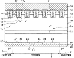
図1に示されるように、半導体装置は、IGBT素子1aを有するIGBT領域1と、FWD素子2aを有するFWD領域2とが共通の半導体基板10に形成されたRC(すなわち、Reverse Conducting)−IGBTとされている。特に限定されるものではないが、本実施形態では、IGBT領域1およびFWD領域2は、一方向に沿って延設されていると共に、延設方向と交差する方向に交互に形成されている。なお、図1中では、IGBT領域1およびFWD領域2は、紙面左右方向に沿って延設され、紙面上下方向に交互に形成されている。
As shown in FIG. 1, the semiconductor device includes an RC (ie, Reverse Conducting) -IGBT in which an
図2に示されるように、半導体基板10は、N−型のドリフト層11を有している。なお、半導体基板10は、例えば、シリコン基板で構成される。そして、ドリフト層11上(すなわち、半導体基板10の一面10a側)には、P型のベース層12が形成されている。
As shown in FIG. 2, the
また、半導体基板10には、ベース層12を貫通してドリフト層11に達するように複数のトレンチ13が形成されている。これにより、ベース層12は、トレンチ13によって複数個に分離されている。本実施形態では、複数のトレンチ13は、IGBT領域1およびFWD領域2にそれぞれ形成され、半導体基板10の一面10aの面方向のうちの一方向に沿って等間隔に形成されたストライプ状とされている。なお、図2中では、各トレンチ13は、紙面垂直方向に沿って形成されている。
A plurality of
各トレンチ13は、各トレンチ13の壁面を覆うように形成されたゲート絶縁膜14と、このゲート絶縁膜14の上に形成されたポリシリコン等により構成されるゲート電極15とにより埋め込まれている。これにより、トレンチゲート構造が構成されている。
Each
ベース層12の表層部(すなわち、半導体基板10の一面10a側)には、ドリフト層11よりも高不純物濃度とされたN+型のエミッタ領域16が形成されている。具体的には、エミッタ領域16は、ベース層12内において終端し、かつ、トレンチ13の側面に接するように形成されている。より詳しくは、エミッタ領域16は、トレンチ13間の領域において、トレンチ13の長手方向に沿ってトレンチ13の側面に接するように棒状に延設され、トレンチ13の先端よりも内側で終端する構造とされている。なお、本実施形態では、トレンチ13の壁面のうちのエミッタ領域16とドリフト層11との間に位置する部分が、エミッタ領域とドリフト層との間に位置するベース層の表面に相当する。
An N + -
半導体基板10の一面10a上には、BPSG(すなわち、Boron Phosphorus Silicon Glass)等で構成される層間絶縁膜17が形成されている。そして、層間絶縁膜17上には、層間絶縁膜17に形成されたコンタクトホール17aを介してエミッタ領域16およびベース層12と電気的に接続される上部電極18が形成されている。つまり、層間絶縁膜17上には、IGBT領域1においてエミッタ電極として機能し、FWD領域2においてアノード電極として機能する上部電極18が形成されている。
On one
なお、本実施形態では、上部電極18が第1電極に相当している。また、図1に示されるように、半導体基板10の一面10a上には、ゲート電極15や図示しない温度センサ等と接続される複数のパッド部19が形成されている。
In the present embodiment, the
そして、図2に示されるように、IGBT領域1では、ドリフト層11のうちのベース層12側と反対側(すなわち、半導体基板10の他面10b側)にP+型のコレクタ層20が形成されている。また、FWD領域2では、ドリフト層11のうちのベース層12側と反対側(すなわち、半導体基板10の他面10b側)にN+型のカソード層21が形成されている。つまり、IGBT領域1とFWD領域2とは、半導体基板10の他面10b側に形成される層がコレクタ層20であるかカソード層21であるかによって区画されている。そして、本実施形態では、コレクタ層20上の部分がIGBT領域1とされ、カソード層21上の部分がFWD領域2とされている。なお、コレクタ層20およびカソード層21は、半導体基板10の他面10bから一面10aに向かって同じ深さまで形成されている。
As shown in FIG. 2, in the
また、ドリフト層11には、ベース層12側と反対側(すなわち、半導体基板10の他面10b側)に、ドリフト層11よりも高不純物濃度とされたN型のFS層22が形成されている。具体的には、FS層22は、コレクタ層20およびカソード層21と離れた位置に形成されている。言い換えると、FS層22は、ドリフト層11内に形成されている。つまり、FS層22は、コレクタ層20およびカソード層21との間にドリフト層11の一部が残存するように形成されている。なお、FS層22は、具体的には後述するが、半導体基板10の厚さL1に対するFS層22とコレクタ層20およびカソード層21との間隔L2の比率が所定値となるように形成されている。
In addition, an N-
コレクタ層20およびカソード層21を挟んでドリフト層11と反対側(すなわち、半導体基板10の他面10b)には、コレクタ層20およびカソード層21と電気的に接続される下部電極23が形成されている。つまり、IGBT領域1においてはコレクタ電極として機能し、FWD領域2においてはカソード電極として機能する下部電極23が形成されている。本実施形態では、下部電極23が第2電極に相当している。
A
そして、上記のように構成されていることにより、FWD領域2においては、ベース層12をアノードとし、ドリフト層11、FS層22、カソード層21をカソードとしてPN接合されたFWD素子2aが構成されている。
With the configuration as described above, in the
以上が本実施形態における半導体装置の構成である。なお、本実施形態では、N型、N+型、N−型が第1導電型に相当しており、P型、P+型が第2導電型に相当している。また、本実施形態では、半導体基板10は、上記のように、コレクタ層20、カソード層21、ドリフト層11、FS層22、ベース層12、エミッタ領域16を含んで構成されている。次に、上記半導体装置の作動について説明する。
The above is the configuration of the semiconductor device in this embodiment. In the present embodiment, the N type, the N + type, and the N − type correspond to the first conductivity type, and the P type and the P + type correspond to the second conductivity type. In the present embodiment, the
まず、半導体装置は、下部電極23に上部電極18より高い電圧が印加されると、ベース層12とドリフト層11との間に形成されるPN接合が逆導通状態となって空乏層が形成される。この際、ゲート電極15に、絶縁ゲート構造の閾値電圧Vth未満であるローレベル(例えば、0V)の電圧が印加されているときには、上部電極18と下部電極23との間に電流は流れない。
First, in the semiconductor device, when a voltage higher than that of the
そして、IGBT素子1aをオン状態にするには、下部電極23に上部電極18より高い電圧が印加された状態で、ゲート電極15に、絶縁ゲート構造の閾値電圧Vth以上であるハイレベルの電圧が印加されるようにする。これにより、ベース層12のうちのトレンチ13と接している部分には、反転層が形成される。そして、IGBT素子1aは、エミッタ領域16から反転層を介して電子がドリフト層11に供給されることによってコレクタ層20から正孔がドリフト層11に供給され、伝導度変調によりドリフト層11の抵抗値が低下することでオン状態となる。
In order to turn on the
また、IGBT素子1aをオフ状態にし、FWD素子2aをオン状態にする(すなわち、FWD素子2aをダイオード動作させる)際には、上部電極18と下部電極23に印加する電圧をスイッチングし、上部電極18に下部電極23より高い電圧を印加する。そして、ゲート電極15に絶縁ゲート構造の閾値電圧Vth未満であるローレベル(例えば、0V)の電圧を印加する。これにより、ベース層12のうちのトレンチ13と接する部分に反転層が形成されなくなり、上部電極18からベース層12を介して正孔が供給されると共に、下部電極23からカソード層21を介して電子が供給されることでFWD素子2aがダイオード動作をする。
Further, when the
その後、FWD素子2aをオン状態からオフ状態にする際には、下部電極23に上部電極18より高い電圧を印加する逆電圧印加を行う。つまり、FWD素子2aに順方向電流が流れている状態から当該電流を遮断する際、下部電極23に上部電極18より高い電圧を印加する逆電圧印加を行う。これにより、FWD素子2aがリカバリ状態となる。そして、ベース層12中の正孔が上部電極18側に引き寄せられると共にドリフト層11中の電子が下部電極23側に引き寄せられることでリカバリ電流が発生し、ベース層12とドリフト層11との間の空乏層が伸びる。
Thereafter, when the
ここで、リカバリ状態では、図3に示されるように、ドリフト層11中の電子の一部がコレクタ層20を介して下部電極23にも流れ込む。そして、コレクタ層20に電子が流れ込むことにより、下部電極23からコレクタ層20を介して正孔がドリフト層11に注入される。
Here, in the recovery state, as shown in FIG. 3, some of the electrons in the
この際、本実施形態の半導体装置では、FS層22がコレクタ層20およびカソード層21から離れて形成されている。このため、本実施形態の半導体装置では、FS層22がコレクタ層20およびカソード層21と接している従来の半導体装置と比較して、コレクタ層20上およびその近傍に位置する領域の内部抵抗が大きくなる。このため、本実施形態の半導体装置では、従来の半導体装置と比較して、電子がコレクタ層20に流れ込む際の電圧降下が大きくなる。つまり、本実施形態の半導体装置では、従来の半導体装置と比較して、コレクタ層20上およびその近傍の領域の電位が低くなり易い。
At this time, in the semiconductor device of this embodiment, the
したがって、本実施形態の半導体装置では、リカバリ状態において、電子がコレクタ層20へと流れ込み易くなり、これに伴ってコレクタ層20を介してドリフト層11に注入される正孔の量が増加する。そして、コレクタ層20から注入される正孔は、半導体基板10の面方向に沿っても広がるため、カソード層21上の領域にも正孔が供給される。このため、本実施形態の半導体装置では、リカバリ状態において、FWD領域2でキャリアが枯渇し難くなり、空乏層が半導体基板10の他面10b側に伸び難くなる。つまり、リカバリ状態において、FWD領域2の空間電荷密度が上昇し、空乏層が半導体基板10の他面10b側に伸び難くなる。これにより、リカバリ状態において、完全空乏化を抑制でき、サージピーク電圧を小さくできる。
Therefore, in the semiconductor device according to the present embodiment, electrons easily flow into the
なお、本実施形態では、電子が第1キャリアに相当し、正孔が第2キャリアに相当している。また、本実施形態のFS層22は、後述するように、リカバリ状態において、サージピーク電圧が小さくなる適量の正孔が注入される位置に形成されている。
In the present embodiment, electrons correspond to first carriers and holes correspond to second carriers. Further, as will be described later, the
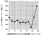
そして、本発明者らは、さらに、サージピーク電圧の大きさと、半導体基板10の厚さL1に対するFS層22とコレクタ層20およびカソード層21との間隔L2の比率について検討を行い、図4に示す結果を得た。
Then, the inventors further examined the magnitude of the surge peak voltage and the ratio of the distance L2 between the
なお、図1に示されるように、半導体基板10の厚さL1とは、半導体基板10の一面10aと他面10bとの間の長さのことである。FS層22とコレクタ層20およびカソード層21との間隔L2とは、FS層22とコレクタ層20およびカソード層21との間の半導体基板10の厚さ方向に沿った長さのことである。図4中では、FS層22とコレクタ層20およびカソード層21との間隔L2を、単にFS層22の間隔と示してある。以下では、半導体基板10の厚さL1に対するFS層22とコレクタ層20およびカソード層21との間隔L2の比率[%]を単にL2/L1として説明する。
As shown in FIG. 1, the thickness L1 of the
図4に示されるように、L2/L1が0の場合を基準とすると、サージピーク電圧は、L2/L1を0から徐々に大きくすると小さくなる。なお、L2/L1が0の場合とは、FS層22がコレクタ層20およびカソード層21と接している場合のことである。
As shown in FIG. 4, on the basis of the case where L2 / L1 is 0, the surge peak voltage decreases as L2 / L1 is gradually increased from 0. The case where L2 / L1 is 0 is a case where the
そして、サージピーク電圧は、L2/L1が2〜17%となる際にほぼ等しくなる。また、サージピーク電圧は、L2/L1が17%よりさらに大きくなるようにすると急峻に小さくなり、L2/L1が約19%となる場合に最も小さくなる。L2/L1が17%から19%の間にサージピーク電圧が急峻に小さくなるのは、ドリフト層11に注入される正孔が増加することにより、サージピーク電圧に到達した時点から定電圧になる時点までの間のサステイン電圧が大きくなることに起因するものである。
The surge peak voltage becomes substantially equal when L2 / L1 is 2 to 17%. Further, the surge peak voltage is sharply reduced when L2 / L1 is further increased from 17%, and is minimized when L2 / L1 is about 19%. The surge peak voltage sharply decreases when L2 / L1 is between 17% and 19% because the number of holes injected into the
しかしながら、サージピーク電圧は、L2/L1が19%より大きくなるようにすると徐々に上昇し、L2/L1が21.5%となる場合、L1/L2が0である場合と同様の大きさとなる。そして、サージピーク電圧は、L2/L1が21.5%より大きくなるようにすると、さらに上昇する。サージピーク電圧がL2/L1を21.5%より大きくした場合にさらに大きくなるのは、L2/L1が大きくなり過ぎることによって正孔が過度に注入され、サステイン電圧がさらに大きくなることでサージピーク電圧が大きくなってしまうためである。つまり、FS層22とコレクタ層20およびカソード層21との間隔L2が広くなり過ぎると、サージピーク電圧が逆に大きくなってしまう。
However, the surge peak voltage gradually increases when L2 / L1 is greater than 19%, and when L2 / L1 is 21.5%, the surge peak voltage is the same as when L1 / L2 is 0. . The surge peak voltage further increases when L2 / L1 is made larger than 21.5%. The surge peak voltage becomes larger when L2 / L1 is made larger than 21.5%. The surge peak is caused by excessive injection of holes when L2 / L1 becomes too large and the sustain voltage further increases. This is because the voltage increases. That is, if the distance L2 between the
したがって、本実施形態では、FS層22は、サージピーク電圧が小さくなる適量の正孔が注入されるように、L2/L1が21.5%未満となる位置に形成されている。より詳しくは、FS層22は、サージピーク電圧が安定して小さくなるように、L2/L1が2〜19%となるように形成されることが好ましい。
Therefore, in the present embodiment, the
なお、図4は、半導体基板10の厚さを80μm、ドリフト層11の不純物濃度を1.0×1014cm−3、FS層22の不純物濃度を1.0×1016cm−3、ベース層12の不純物濃度を2.5×1017cm−3、カソード層21の不純物濃度を5.0×1019cm−3としたときのシミュレーション結果である。但し、不純物濃度等を変更したとしても、サージピーク電圧の大きさは変化するが、サージピーク電圧の波形と、L2/L1との関係は変化しない。つまり、L2/L1が21.5%未満となるようにFS層22を形成することにより、不純物濃度等に関わらずサージピーク電圧を小さくできる。
4 shows that the thickness of the
以上説明したように、本実施形態では、FS層22をコレクタ層20およびカソード層21と離れた位置に形成している。そして、リカバリ状態において、サージピーク電圧を小さくできるように、コレクタ層20から適量の正孔がドリフト層11に注入されるようにしている。つまり、L1/L2が21.5%未満となるようにしている。このため、サージピーク電圧を小さくでき、半導体装置が破壊されることを抑制できる。
As described above, in this embodiment, the
(第2実施形態)
第2実施形態について説明する。第2実施形態は、第1実施形態に対して、カソード層21内にキャリア注入層を形成したものであり、その他に関しては第1実施形態と同様であるため、ここでは説明を省略する。
(Second Embodiment)
A second embodiment will be described. In the second embodiment, a carrier injection layer is formed in the
本実施形態では、図5に示されるように、カソード層21内にP+型のキャリア注入層24が複数形成されている。本実施形態では、複数のキャリア注入層24は、カソード層21の延設方向に沿ってストライプ状となるように形成されている。
In this embodiment, as shown in FIG. 5, a plurality of P + type carrier injection layers 24 are formed in the
これによれば、リカバリ状態では、ドリフト層11内の正孔は、コレクタ層20と共にカソード層21内に位置するキャリア注入層24にも流れ込む。そして、ドリフト層11には、キャリア注入層24を介しても正孔が注入される。このため、リカバリ状態において、FWD領域2でさらにキャリアが枯渇し難くなり、サージピーク電圧を小さくできる。
According to this, in the recovery state, the holes in the
なお、上記のように、リカバリ状態では、正孔が過度に注入されるとサージピーク電圧が逆に大きくなってしまう。このため、FS層22は、サージピーク電圧が小さくなる適量の正孔が注入されるように、コレクタ層20およびカソード層21との間隔L2が調整された位置に形成されている。
As described above, in the recovery state, when holes are excessively injected, the surge peak voltage is increased. For this reason, the
(他の実施形態)
本発明は上記した実施形態に限定されるものではなく、特許請求の範囲に記載した範囲内において適宜変更が可能である。
(Other embodiments)
The present invention is not limited to the embodiment described above, and can be appropriately changed within the scope described in the claims.
例えば、上記第1実施形態では、第1導電型をN型とし、第2導電型をP型とした例について説明したが、第1導電型をP型とし、第2導電型をN型とすることもできる。 For example, in the first embodiment, an example in which the first conductivity type is N type and the second conductivity type is P type has been described. However, the first conductivity type is P type, and the second conductivity type is N type. You can also
また、上記各実施形態において、ベース層12の表層部(すなわち、半導体基板10の一面10a側)に、ベース層12よりも高不純物濃度とされたP+型のコンタクト領域を形成するようにしてもよい。
In each of the above embodiments, a P + -type contact region having a higher impurity concentration than that of the
そして、上記各実施形態において、FS層22は、半導体基板10の厚さ方向に複数形成されていてもよい。例えば、第1実施形態において、図6に示されるように、FS層22は、半導体基板10の厚さ方向に沿って2つ形成されていてもよい。この場合は、サージピーク電圧が小さくなる適量の正孔が注入されるように、最も半導体基板10の他面10b側に位置するFS層22とコレクタ層20およびカソード層21との間隔L2が上記第1実施形態と同様となるように調整されていればよい。
In each of the above embodiments, a plurality of FS layers 22 may be formed in the thickness direction of the
さらに、上記各実施形態において、トレンチゲート型の半導体装置ではなく、半導体基板10の一面10a上にゲート電極15が配置されるプレーナ型の半導体装置としてもよい。この場合は、半導体基板10の一面10a上にゲート絶縁膜14を介してゲート電極15が配置されるため、ベース層12のうちの半導体基板10の一面10aを構成する部分がベース層の表面に相当する。
Furthermore, in each of the above embodiments, a planar semiconductor device in which the
また、上記第2実施形態において、複数のキャリア注入層24は、ストライプ状ではなく、例えば、格子状に形成されていてもよい。また、キャリア注入層24は複数ではなく、1つのみ形成されていてもよい。
In the second embodiment, the plurality of carrier injection layers 24 may be formed in a lattice shape instead of a stripe shape, for example. Moreover, the
1 IGBT領域
1a IGBT素子
2 FWD領域
2a FWD素子
10 半導体基板
11 ドリフト層
12 ベース層
14 ゲート絶縁膜
15 ゲート電極
16 エミッタ領域
18 上部電極(第1電極)
20 コレクタ層
21 カソード層
22 FS層
23 下部電極(第2電極)
DESCRIPTION OF
20
Claims (5)
第1導電型のドリフト層(11)と、
前記ドリフト層上に形成された第2導電型のベース層(12)と、
前記ベース層の表層部であって、前記ベース層を挟んで前記ドリフト層から離れた位置に形成され、前記ドリフト層よりも高不純物濃度とされた第1導電型のエミッタ領域(16)と、
前記ドリフト層を挟んで前記ベース層と反対側であって、前記IGBT領域に形成された第2導電型のコレクタ層(20)と、
前記ドリフト層を挟んで前記ベース層と反対側であって、前記FWD領域に形成され、前記コレクタ層と隣接する第1導電型のカソード層(21)と、
前記ベース層と、前記コレクタ層および前記カソード層との間に形成されたフィールドストップ層(22)と、を有する前記半導体基板と、
前記エミッタ領域と前記ドリフト層との間に位置する前記ベース層の表面に配置されたゲート絶縁膜(14)と、
前記ゲート絶縁膜上に配置されたゲート電極(15)と、
前記ベース層および前記エミッタ領域と電気的に接続される第1電極(18)と、
前記コレクタ層および前記カソード層と電気的に接続される第2電極(23)と、を備え、
前記フィールドストップ層は、前記コレクタ層および前記カソード層から離れて形成されており、
前記FWD素子に順方向電流が流れている状態から当該電流を遮断してリカバリ状態となった際、前記FWD素子内の第1キャリアの一部が前記コレクタ層へと流れることにより、サージピーク電圧を小さくする量の第2キャリアが前記第2電極から前記コレクタ層を介して前記ドリフト層に注入される半導体装置。 In a semiconductor device in which an IGBT region (1) having an IGBT element (1a) and an FWD region (2) having an FWD element (2a) are formed on a common semiconductor substrate (10),
A first conductivity type drift layer (11);
A second conductivity type base layer (12) formed on the drift layer;
A first conductivity type emitter region (16), which is a surface layer portion of the base layer, formed at a position away from the drift layer with the base layer interposed therebetween, and having a higher impurity concentration than the drift layer;
A second conductivity type collector layer (20) formed in the IGBT region on the opposite side of the base layer across the drift layer;
A cathode layer (21) of the first conductivity type formed on the FWD region on the opposite side of the drift layer and adjacent to the collector layer;
The semiconductor substrate comprising the base layer and a field stop layer (22) formed between the collector layer and the cathode layer;
A gate insulating film (14) disposed on a surface of the base layer located between the emitter region and the drift layer;
A gate electrode (15) disposed on the gate insulating film;
A first electrode (18) electrically connected to the base layer and the emitter region;
A second electrode (23) electrically connected to the collector layer and the cathode layer,
The field stop layer is formed away from the collector layer and the cathode layer;
When a forward current flows through the FWD element, the current is cut off and a recovery state is established, so that a part of the first carrier in the FWD element flows to the collector layer, thereby causing a surge peak voltage. The second carrier is injected into the drift layer from the second electrode through the collector layer so as to reduce the amount of the second carrier.
Priority Applications (2)
| Application Number | Priority Date | Filing Date | Title |
|---|---|---|---|
| JP2017117072A JP2019004030A (en) | 2017-06-14 | 2017-06-14 | Semiconductor device |
| PCT/JP2018/020231 WO2018230312A1 (en) | 2017-06-14 | 2018-05-25 | Semiconductor device |
Applications Claiming Priority (1)
| Application Number | Priority Date | Filing Date | Title |
|---|---|---|---|
| JP2017117072A JP2019004030A (en) | 2017-06-14 | 2017-06-14 | Semiconductor device |
Publications (2)
| Publication Number | Publication Date |
|---|---|
| JP2019004030A true JP2019004030A (en) | 2019-01-10 |
| JP2019004030A5 JP2019004030A5 (en) | 2019-09-19 |
Family
ID=64660825
Family Applications (1)
| Application Number | Title | Priority Date | Filing Date |
|---|---|---|---|
| JP2017117072A Pending JP2019004030A (en) | 2017-06-14 | 2017-06-14 | Semiconductor device |
Country Status (2)
| Country | Link |
|---|---|
| JP (1) | JP2019004030A (en) |
| WO (1) | WO2018230312A1 (en) |
Cited By (1)
| Publication number | Priority date | Publication date | Assignee | Title |
|---|---|---|---|---|
| WO2020148959A1 (en) | 2019-01-15 | 2020-07-23 | ソニー株式会社 | Server and learning system |
Citations (10)
| Publication number | Priority date | Publication date | Assignee | Title |
|---|---|---|---|---|
| WO2007055352A1 (en) * | 2005-11-14 | 2007-05-18 | Fuji Electric Device Technology Co., Ltd. | Semiconductor device and method for manufacturing same |
| JP2012142537A (en) * | 2010-12-16 | 2012-07-26 | Mitsubishi Electric Corp | Insulated gate type bipolar transistor, and method of manufacturing the same |
| JP2013065735A (en) * | 2011-09-19 | 2013-04-11 | Denso Corp | Semiconductor device |
| JP2013089874A (en) * | 2011-10-20 | 2013-05-13 | Denso Corp | Semiconductor device |
| JP2015103697A (en) * | 2013-11-26 | 2015-06-04 | 三菱電機株式会社 | Semiconductor device |
| JP2015177057A (en) * | 2014-03-14 | 2015-10-05 | 株式会社東芝 | semiconductor device |
| JP2015213193A (en) * | 2015-07-21 | 2015-11-26 | ルネサスエレクトロニクス株式会社 | Igbt |
| JP2016006891A (en) * | 2011-07-27 | 2016-01-14 | トヨタ自動車株式会社 | Diode, semiconductor device, and mosfet |
| JP2016111077A (en) * | 2014-12-03 | 2016-06-20 | 三菱電機株式会社 | Semiconductor device for power |
| EP3154091A1 (en) * | 2015-10-07 | 2017-04-12 | ABB Technology AG | Reverse-conducting semiconductor device |
-
2017
- 2017-06-14 JP JP2017117072A patent/JP2019004030A/en active Pending
-
2018
- 2018-05-25 WO PCT/JP2018/020231 patent/WO2018230312A1/en active Application Filing
Patent Citations (10)
| Publication number | Priority date | Publication date | Assignee | Title |
|---|---|---|---|---|
| WO2007055352A1 (en) * | 2005-11-14 | 2007-05-18 | Fuji Electric Device Technology Co., Ltd. | Semiconductor device and method for manufacturing same |
| JP2012142537A (en) * | 2010-12-16 | 2012-07-26 | Mitsubishi Electric Corp | Insulated gate type bipolar transistor, and method of manufacturing the same |
| JP2016006891A (en) * | 2011-07-27 | 2016-01-14 | トヨタ自動車株式会社 | Diode, semiconductor device, and mosfet |
| JP2013065735A (en) * | 2011-09-19 | 2013-04-11 | Denso Corp | Semiconductor device |
| JP2013089874A (en) * | 2011-10-20 | 2013-05-13 | Denso Corp | Semiconductor device |
| JP2015103697A (en) * | 2013-11-26 | 2015-06-04 | 三菱電機株式会社 | Semiconductor device |
| JP2015177057A (en) * | 2014-03-14 | 2015-10-05 | 株式会社東芝 | semiconductor device |
| JP2016111077A (en) * | 2014-12-03 | 2016-06-20 | 三菱電機株式会社 | Semiconductor device for power |
| JP2015213193A (en) * | 2015-07-21 | 2015-11-26 | ルネサスエレクトロニクス株式会社 | Igbt |
| EP3154091A1 (en) * | 2015-10-07 | 2017-04-12 | ABB Technology AG | Reverse-conducting semiconductor device |
Cited By (1)
| Publication number | Priority date | Publication date | Assignee | Title |
|---|---|---|---|---|
| WO2020148959A1 (en) | 2019-01-15 | 2020-07-23 | ソニー株式会社 | Server and learning system |
Also Published As
| Publication number | Publication date |
|---|---|
| WO2018230312A1 (en) | 2018-12-20 |
Similar Documents
| Publication | Publication Date | Title |
|---|---|---|
| JP6443267B2 (en) | Semiconductor device | |
| JP6589817B2 (en) | Semiconductor device | |
| JP5787853B2 (en) | Power semiconductor device | |
| JP5103830B2 (en) | Insulated gate semiconductor device | |
| WO2017199679A1 (en) | Semiconductor device | |
| JP2016136620A (en) | Semiconductor device | |
| JP5480084B2 (en) | Semiconductor device | |
| JP2016157934A (en) | Semiconductor device | |
| JP2007184486A (en) | Semiconductor device | |
| JP2013098415A (en) | Semiconductor device | |
| JP2017135339A (en) | Semiconductor device | |
| CN107148675A (en) | Semiconductor device | |
| JPH09283754A (en) | High withstand voltage semiconductor device | |
| CN109314143A (en) | Semiconductor device | |
| JP2008311301A (en) | Insulated gate bipolar transistor | |
| JP5537359B2 (en) | Semiconductor device | |
| CN109509789A (en) | Semiconductor device | |
| JP2016092163A (en) | Semiconductor device | |
| JP2018041845A (en) | Semiconductor device | |
| JP2011238681A (en) | Semiconductor device | |
| US20170309704A1 (en) | Semiconductor device and manufacturing method therefor | |
| JP2014154739A (en) | Semiconductor device | |
| CN111344867B (en) | Semiconductor device with a semiconductor device having a plurality of semiconductor chips | |
| WO2018230312A1 (en) | Semiconductor device | |
| JP2020043237A (en) | Semiconductor device |
Legal Events
| Date | Code | Title | Description |
|---|---|---|---|
| A521 | Request for written amendment filed |
Free format text: JAPANESE INTERMEDIATE CODE: A523 Effective date: 20190808 |
|
| A621 | Written request for application examination |
Free format text: JAPANESE INTERMEDIATE CODE: A621 Effective date: 20190808 |
|
| A131 | Notification of reasons for refusal |
Free format text: JAPANESE INTERMEDIATE CODE: A131 Effective date: 20200602 |
|
| A521 | Request for written amendment filed |
Free format text: JAPANESE INTERMEDIATE CODE: A523 Effective date: 20200731 |
|
| A02 | Decision of refusal |
Free format text: JAPANESE INTERMEDIATE CODE: A02 Effective date: 20201013 |