JP2014103263A - 基板処理装置、基板処理方法及び記憶媒体 - Google Patents
基板処理装置、基板処理方法及び記憶媒体 Download PDFInfo
- Publication number
- JP2014103263A JP2014103263A JP2012254424A JP2012254424A JP2014103263A JP 2014103263 A JP2014103263 A JP 2014103263A JP 2012254424 A JP2012254424 A JP 2012254424A JP 2012254424 A JP2012254424 A JP 2012254424A JP 2014103263 A JP2014103263 A JP 2014103263A
- Authority
- JP
- Japan
- Prior art keywords
- substrate
- housing
- flow rate
- cup
- gas
- Prior art date
- Legal status (The legal status is an assumption and is not a legal conclusion. Google has not performed a legal analysis and makes no representation as to the accuracy of the status listed.)
- Granted
Links
- 239000000758 substrate Substances 0.000 title claims abstract description 107
- 238000003672 processing method Methods 0.000 title claims description 11
- 238000003860 storage Methods 0.000 title claims description 11
- 239000007788 liquid Substances 0.000 claims abstract description 123
- 238000001035 drying Methods 0.000 claims abstract description 43
- 238000000034 method Methods 0.000 claims abstract description 35
- 239000007789 gas Substances 0.000 claims description 90
- KFZMGEQAYNKOFK-UHFFFAOYSA-N Isopropanol Chemical compound CC(C)O KFZMGEQAYNKOFK-UHFFFAOYSA-N 0.000 claims description 27
- IJGRMHOSHXDMSA-UHFFFAOYSA-N Atomic nitrogen Chemical compound N#N IJGRMHOSHXDMSA-UHFFFAOYSA-N 0.000 claims description 19
- 229910001873 dinitrogen Inorganic materials 0.000 claims description 19
- 239000012530 fluid Substances 0.000 claims description 11
- 230000002093 peripheral effect Effects 0.000 claims description 8
- 238000007599 discharging Methods 0.000 claims description 4
- 238000004140 cleaning Methods 0.000 abstract description 24
- 239000000126 substance Substances 0.000 description 56
- 230000002378 acidificating effect Effects 0.000 description 39
- 230000007246 mechanism Effects 0.000 description 8
- 239000003595 mist Substances 0.000 description 8
- 239000002253 acid Substances 0.000 description 3
- 230000001174 ascending effect Effects 0.000 description 3
- 239000010808 liquid waste Substances 0.000 description 3
- 238000004519 manufacturing process Methods 0.000 description 3
- 239000002245 particle Substances 0.000 description 3
- 239000004065 semiconductor Substances 0.000 description 3
- KRHYYFGTRYWZRS-UHFFFAOYSA-N Fluorane Chemical compound F KRHYYFGTRYWZRS-UHFFFAOYSA-N 0.000 description 2
- QVGXLLKOCUKJST-UHFFFAOYSA-N atomic oxygen Chemical compound [O] QVGXLLKOCUKJST-UHFFFAOYSA-N 0.000 description 2
- 210000000078 claw Anatomy 0.000 description 2
- 230000001276 controlling effect Effects 0.000 description 2
- 238000010586 diagram Methods 0.000 description 2
- 239000001301 oxygen Substances 0.000 description 2
- 229910052760 oxygen Inorganic materials 0.000 description 2
- 238000011144 upstream manufacturing Methods 0.000 description 2
- 238000001311 chemical methods and process Methods 0.000 description 1
- 238000011109 contamination Methods 0.000 description 1
- 230000007423 decrease Effects 0.000 description 1
- 230000003247 decreasing effect Effects 0.000 description 1
- 238000005516 engineering process Methods 0.000 description 1
- 238000001914 filtration Methods 0.000 description 1
- 238000012423 maintenance Methods 0.000 description 1
- 230000014759 maintenance of location Effects 0.000 description 1
- 230000001105 regulatory effect Effects 0.000 description 1
- 238000009423 ventilation Methods 0.000 description 1
- XLYOFNOQVPJJNP-UHFFFAOYSA-N water Substances O XLYOFNOQVPJJNP-UHFFFAOYSA-N 0.000 description 1
Images

Classifications
-
- H—ELECTRICITY
- H01—ELECTRIC ELEMENTS
- H01L—SEMICONDUCTOR DEVICES NOT COVERED BY CLASS H10
- H01L21/00—Processes or apparatus adapted for the manufacture or treatment of semiconductor or solid state devices or of parts thereof
- H01L21/02—Manufacture or treatment of semiconductor devices or of parts thereof
- H01L21/04—Manufacture or treatment of semiconductor devices or of parts thereof the devices having potential barriers, e.g. a PN junction, depletion layer or carrier concentration layer
- H01L21/18—Manufacture or treatment of semiconductor devices or of parts thereof the devices having potential barriers, e.g. a PN junction, depletion layer or carrier concentration layer the devices having semiconductor bodies comprising elements of Group IV of the Periodic Table or AIIIBV compounds with or without impurities, e.g. doping materials
- H01L21/30—Treatment of semiconductor bodies using processes or apparatus not provided for in groups H01L21/20 - H01L21/26
- H01L21/302—Treatment of semiconductor bodies using processes or apparatus not provided for in groups H01L21/20 - H01L21/26 to change their surface-physical characteristics or shape, e.g. etching, polishing, cutting
-
- H—ELECTRICITY
- H01—ELECTRIC ELEMENTS
- H01L—SEMICONDUCTOR DEVICES NOT COVERED BY CLASS H10
- H01L21/00—Processes or apparatus adapted for the manufacture or treatment of semiconductor or solid state devices or of parts thereof
- H01L21/02—Manufacture or treatment of semiconductor devices or of parts thereof
- H01L21/02041—Cleaning
- H01L21/02043—Cleaning before device manufacture, i.e. Begin-Of-Line process
- H01L21/02052—Wet cleaning only
-
- H—ELECTRICITY
- H01—ELECTRIC ELEMENTS
- H01L—SEMICONDUCTOR DEVICES NOT COVERED BY CLASS H10
- H01L21/00—Processes or apparatus adapted for the manufacture or treatment of semiconductor or solid state devices or of parts thereof
- H01L21/67—Apparatus specially adapted for handling semiconductor or electric solid state devices during manufacture or treatment thereof; Apparatus specially adapted for handling wafers during manufacture or treatment of semiconductor or electric solid state devices or components ; Apparatus not specifically provided for elsewhere
- H01L21/67005—Apparatus not specifically provided for elsewhere
- H01L21/67011—Apparatus for manufacture or treatment
- H01L21/67017—Apparatus for fluid treatment
- H01L21/67028—Apparatus for fluid treatment for cleaning followed by drying, rinsing, stripping, blasting or the like
- H01L21/6704—Apparatus for fluid treatment for cleaning followed by drying, rinsing, stripping, blasting or the like for wet cleaning or washing
- H01L21/67051—Apparatus for fluid treatment for cleaning followed by drying, rinsing, stripping, blasting or the like for wet cleaning or washing using mainly spraying means, e.g. nozzles
Landscapes
- Engineering & Computer Science (AREA)
- Physics & Mathematics (AREA)
- Condensed Matter Physics & Semiconductors (AREA)
- General Physics & Mathematics (AREA)
- Manufacturing & Machinery (AREA)
- Computer Hardware Design (AREA)
- Microelectronics & Electronic Packaging (AREA)
- Power Engineering (AREA)
- Cleaning Or Drying Semiconductors (AREA)
- Weting (AREA)
- Exposure Of Semiconductors, Excluding Electron Or Ion Beam Exposure (AREA)
Abstract
【解決手段】基板(W)に液処理を行っているときに清浄ガス供給装置(70,78)からハウジング(60)の内部空間に供給される清浄ガス(70)の流量よりも、基板に乾燥処理を行っているときに清浄ガス供給装置から供給される低湿度の清浄ガス(78)の流量を小さくし、かつ、液処理を行っているときにハウジング排気路(64)を通って排気されるガスの流量よりも、乾燥処理を行っているときにハウジング排気路を通って排気されるガスの流量を小さくする。
【選択図】図1
Description
ウエハWが基板処理部10により保持され、回転駆動部18によりウエハWが回転する。この回転するウエハWには、処理液として、酸性薬液ノズル51から酸性薬液例えばDHFが供給され、ウエハWに酸性薬液洗浄処理が施される。酸性薬液は遠心力によりウエハWから振り切られ、回転カップ20に受け止められる。このとき、第2カップ32及び第3カップ33が下降位置に位置しており、酸性薬液は第1カップ31と第2カップと32との間の第1流路311を通って流れる。
次に、ウエハWの回転を継続したまま、酸性薬液ノズル51からの酸性薬液の吐出を停止し、代わりに、リンス液ノズル53から、処理液として、リンス液例えばDIWをウエハWに供給する。これによりウエハW上に残留する酸性薬液及び残渣が洗い流される。このリンス処理は、上記の点のみが酸性薬液洗浄処理と異なり、その他の点(ガス、処理液等の流れ)は酸性薬液洗浄処理と同じである。
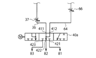
次に、ウエハWの回転を継続したまま、リンス液ノズル53からのリンス液の吐出を停止し、第3カップ33を下降位置に維持したまま第2カップ32を上昇位置に移動させ、切替弁40を切り替えてカップ排気路36とアルカリ性雰囲気排気ライン82とを連通させる。次いで、ウエハWに、処理液として、アルカリ性薬液ノズル52からアルカリ性洗浄液例えばSC−1がウエハに供給され、ウエハWにアルカリ性薬液洗浄処理が施される。このアルカリ性薬液洗浄処理は、ガス及びアルカリ性薬液の排出経路が酸性薬液洗浄処理と異なり、他の点については酸性薬液洗浄処理と同じである。
次に、ウエハWの回転を継続したまま、アルカリ性薬液ノズル52からのアルカリ性薬液の吐出を停止し、代わりに、リンス液ノズル53から、リンス液をウエハWに供給する。これによりウエハW上に残留するアルカリ性薬液及び残渣が洗い流される。この第2リンス処理は、ガス及び処理液(リンス液)の排出経路が第1リンス処理と異なり、他の点については第1リンス処理と同じである。
次に、ウエハWの回転を継続したまま、リンス液ノズル53からのリンス液の吐出を停止し、第2カップ32を上昇位置に維持したまま第3カップ33を上昇位置に移動させ(このときに図1に示す状態となる)、切替弁40を切り替えてカップ排気路36と有機雰囲気排気ライン83とを連通させる。これとほぼ同時に、FFU70のファン71が停止され、続いてダンパ74が閉じられる。その後直ちに、ガスノズル78から窒素ガス(ドライエアでもよい)が吐出される。次いで、処理液として、乾燥促進液ノズル54から所定時間だけ乾燥促進液例えばIPAがウエハWに供給され、その後乾燥促進液ノズル54からの乾燥促進液の供給が停止され、ウエハWの回転が所定時間継続される。これにより、ウエハW上に残留していたDIWがIPA中に取り込まれ、このIPAがウエハW上から振り切られるとともに蒸発し、ウエハWの乾燥が行われる。
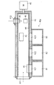
10 基板保持部
18 回転駆動部
30カップ体
36 カップ排気路
40、66 排気流量調整部(切替弁、流量調整弁)
51〜54 処理液ノズル
60 ハウジング
64 ハウジング排気路
70、78 清浄ガス供給装置(FFU、ガスノズル)
100 制御部(コントローラ)
Claims (12)
- 基板を水平姿勢で保持する基板保持部と、
前記基板保持部を鉛直軸線周りに回転させる回転駆動部と、
前記基板に処理液を供給する処理液ノズルと、
前記基板保持部に保持された基板の周囲を囲んで処理液を回収する、上部が開放されたカップ体と、
前記基板保持部、前記ノズルおよび前記カップ体が収容される内部空間を有するハウジングと、
前記ハウジングの内部空間の前記カップ体の上方の領域に第1清浄ガスと前記第1清浄ガスよりも湿度が低い第2清浄ガスを切り替えて供給する清浄ガス供給装置と、
前記カップ体の内部の雰囲気を吸引するためのカップ排気路と、
前記ハウジングの内部空間であってかつ前記カップ体の外部に設けられた吸入口を有し、前記カップ体の内部を介さずに前記ハウジングの内部空間の雰囲気を吸引するためのハウジング排気路と、
前記ハウジング排気路に設けられた排気流量調整部と、
基板に前記処理液ノズルから処理液を供給して液処理を行っているときに供給される第1清浄ガスの流量よりも、基板に乾燥処理を行っているときに前記清浄ガス供給装置から供給される第2清浄ガスの流量を小さくするとともに、前記液処理を行っているときに前記ハウジング排気路を通って排気されるガスの流量よりも、前記乾燥処理を行っているときに前記ハウジング排気路を通って排気されるガスの流量を小さくするように前記排気流量調整部を制御する制御部と、
を備えた基板処理装置。 - 前記制御部は、前記液処理を行っているときに前記カップ排気路を通って排気されるガスの流量よりも、前記乾燥処理を行っているときに前記カップ排気路を通って排気されるガスの流量を小さくするように制御する、
請求項1に記載の基板処理装置。 - 前記第1清浄ガスは、ファンフィルタユニット(FFU)を介して供給される濾過されたクリーンルーム内の空気であり、前記第2清浄ガスは、クリーンドライエアまたは窒素ガスである、請求項1または2に記載の基板処理装置。
- 前記基板処理装置は、前記乾燥処理を行うときに前記基板に乾燥促進流体を供給する乾燥促進流体ノズルをさらに備えている、請求項1〜3のうちのいずれか一項に記載の基板処理装置。
- 前記乾燥促進流体はイソプロピルアルコールからなる、請求項4記載の基板処理装置。
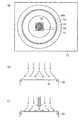
- 前記清浄ガス供給装置は、前記ハウジングの内部空間に面した整流板を有しており、整流板には前記清浄ガスを前記ハウジングの内部空間に向けて下方に吐出する複数の開口が形成されており、
前記基板保持部に基板が保持された場合、前記基板の中央部の真上にある前記整流板の領域の開口率が、前記基板の周縁部の真上にある前記整流板の領域の開口率よりも大きい、請求項1〜5のいずれか一項に記載の基板処理装置。 - 基板を水平姿勢で保持する基板保持部と、
前記基板保持部を鉛直軸線周りに回転させる回転駆動部と、
前記基板に処理液を供給する処理液ノズルと、
前記基板保持部に保持された基板の周囲を囲んで処理液を回収する、上部が開放されたカップ体と、
前記基板保持部、前記ノズルおよび前記カップ体が収容される内部空間を有するハウジングと、
前記ハウジングの内部空間の前記カップ体の上方の領域に第1清浄ガスと前記第1清浄ガスよりも湿度が低い第2清浄ガスを切り替えて供給する清浄ガス供給装置と、
前記カップ体の内部の雰囲気を吸引するためのカップ排気路と、
前記ハウジングの内部空間であってかつ前記カップ体の外部に設けられた吸入口を有し、前記カップ体の内部を介さずに前記ハウジングの内部空間の雰囲気を吸引するためのハウジング排気路と、
前記ハウジング排気路に設けられた排気流量調整部と、
を備えた基板処理装置を用いて実行される基板処理方法であって、
基板に前記処理液ノズルから処理液を供給して液処理を行っているときに供給される第1清浄ガスの流量よりも、基板に乾燥処理を行っているときに前記清浄ガス供給装置から供給される第2清浄ガスの流量を小さくし、かつ、前記液処理を行っているときに前記ハウジング排気路を通って排気されるガスの流量よりも、前記乾燥処理を行っているときに前記ハウジング排気路を通って排気されるガスの流量を小さくすることを特徴とする基板処理方法。 - 前記液処理を行っているときに前記カップ排気路を通って排気されるガスの流量よりも、前記乾燥処理を行っているときに前記カップ排気路を通って排気されるガスの流量を小さくする、
請求項7に記載の基板処理方法。 - 前記第1清浄ガスは、ファンフィルタユニット(FFU)を介して供給される濾過されたクリーンルーム内の空気であり、前記第2清浄ガスは、クリーンドライエアまたは窒素ガスである、請求項7または8に記載の基板処理方法。
- 前記基板処理装置は、乾燥促進流体ノズルをさらに備えており、前記乾燥処理を行っているときに、前記乾燥促進流体ノズルから前記基板保持部に保持された基板に乾燥促進流体が供給される、請求項7〜9のうちのいずれか一項に記載の基板処理方法。
- 前記乾燥促進流体はイソプロピルアルコールからなる、請求項9記載の基板処理方法。
- 基板処理装置を制御するためのプログラムが記憶された記憶媒体であって、当該記憶媒体に記憶されたプログラムをコンピュータからなる前記基板処理装置のコントローラで実行することにより、前記コントローラが前記基板処理装置を制御して請求項7〜11のうちのいずれか一項に記載の基板処理方法を実行する、記憶媒体。
Priority Applications (4)
| Application Number | Priority Date | Filing Date | Title |
|---|---|---|---|
| JP2012254424A JP6026241B2 (ja) | 2012-11-20 | 2012-11-20 | 基板処理装置、基板処理方法及び記憶媒体 |
| TW102141258A TWI547986B (zh) | 2012-11-20 | 2013-11-13 | A substrate processing apparatus, a substrate processing method, and a memory medium |
| KR1020130140481A KR101949722B1 (ko) | 2012-11-20 | 2013-11-19 | 기판 처리 장치, 기판 처리 방법 및 기억 매체 |
| US14/083,673 US20140137893A1 (en) | 2012-11-20 | 2013-11-19 | Substrate processing apparatus, substrate processing method and storage medium |
Applications Claiming Priority (1)
| Application Number | Priority Date | Filing Date | Title |
|---|---|---|---|
| JP2012254424A JP6026241B2 (ja) | 2012-11-20 | 2012-11-20 | 基板処理装置、基板処理方法及び記憶媒体 |
Publications (3)
| Publication Number | Publication Date |
|---|---|
| JP2014103263A true JP2014103263A (ja) | 2014-06-05 |
| JP2014103263A5 JP2014103263A5 (ja) | 2015-04-30 |
| JP6026241B2 JP6026241B2 (ja) | 2016-11-16 |
Family
ID=50726750
Family Applications (1)
| Application Number | Title | Priority Date | Filing Date |
|---|---|---|---|
| JP2012254424A Active JP6026241B2 (ja) | 2012-11-20 | 2012-11-20 | 基板処理装置、基板処理方法及び記憶媒体 |
Country Status (4)
| Country | Link |
|---|---|
| US (1) | US20140137893A1 (ja) |
| JP (1) | JP6026241B2 (ja) |
| KR (1) | KR101949722B1 (ja) |
| TW (1) | TWI547986B (ja) |
Cited By (5)
| Publication number | Priority date | Publication date | Assignee | Title |
|---|---|---|---|---|
| US20160020122A1 (en) * | 2014-07-15 | 2016-01-21 | Tokyo Electron Limited | Substrate processing apparatus and substrate processing method |
| KR20190103020A (ko) * | 2018-02-27 | 2019-09-04 | 도쿄엘렉트론가부시키가이샤 | 기판 처리 장치, 기판 처리 방법 및 컴퓨터 판독 가능한 기록 매체 |
| KR20200115104A (ko) * | 2019-03-28 | 2020-10-07 | 가부시키가이샤 스크린 홀딩스 | 기판 처리 장치, 기판 처리 방법, 및 반도체 제조 방법 |
| JP2021057596A (ja) * | 2015-11-30 | 2021-04-08 | アプライド マテリアルズ インコーポレイテッドApplied Materials,Incorporated | フォトレジストウエハの露光後プロセスの方法及び装置 |
| JP2021103701A (ja) * | 2019-12-24 | 2021-07-15 | 東京エレクトロン株式会社 | 液処理装置、液処理方法及びコンピュータ読み取り可能な記録媒体 |
Families Citing this family (14)
| Publication number | Priority date | Publication date | Assignee | Title |
|---|---|---|---|---|
| US9698029B2 (en) * | 2014-02-19 | 2017-07-04 | Lam Research Ag | Method and apparatus for processing wafer-shaped articles |
| KR102232664B1 (ko) * | 2014-05-28 | 2021-03-30 | 세메스 주식회사 | 기판 처리 장치 및 기판 처리 시스템 |
| KR102387542B1 (ko) * | 2017-05-11 | 2022-04-19 | 주식회사 케이씨텍 | 에어공급부 및 기판 처리 장치 |
| JP6887912B2 (ja) * | 2017-08-07 | 2021-06-16 | 東京エレクトロン株式会社 | 基板処理装置、基板処理方法及び記憶媒体 |
| JP7015219B2 (ja) * | 2018-06-29 | 2022-02-02 | 株式会社Screenホールディングス | 基板処理方法および基板処理装置 |
| KR102201879B1 (ko) * | 2018-09-07 | 2021-01-12 | 세메스 주식회사 | 기판 처리 장치 및 방법 |
| JP7314634B2 (ja) * | 2019-06-11 | 2023-07-26 | 東京エレクトロン株式会社 | 塗布装置及び塗布方法 |
| KR102351341B1 (ko) * | 2019-12-09 | 2022-01-18 | 무진전자 주식회사 | 팬 필터 유닛 및 이를 포함하는 기판 처리 장치 |
| US20210265177A1 (en) * | 2020-02-26 | 2021-08-26 | SCREEN Holdings Co., Ltd. | Substrate treating apparatus |
| KR102388473B1 (ko) * | 2020-08-11 | 2022-04-20 | (주)마스 | 클린 건조 공기 셔터 팬 필터 유닛 |
| KR20220131680A (ko) * | 2021-03-22 | 2022-09-29 | 세메스 주식회사 | 기판 처리 장치 |
| JP2023013349A (ja) * | 2021-07-15 | 2023-01-26 | 株式会社Screenホールディングス | 基板洗浄装置、基板洗浄システム、基板処理システム、基板洗浄方法および基板処理方法 |
| KR102571523B1 (ko) * | 2021-09-10 | 2023-08-29 | (주)디바이스이엔지 | 배기구조를 포함하는 기판 처리장치 |
| KR102646155B1 (ko) * | 2022-10-05 | 2024-03-12 | 엘에스이 주식회사 | 기판 세정 장치 |
Citations (4)
| Publication number | Priority date | Publication date | Assignee | Title |
|---|---|---|---|---|
| JPH09148231A (ja) * | 1995-11-16 | 1997-06-06 | Dainippon Screen Mfg Co Ltd | 回転式基板処理装置 |
| JPH09148226A (ja) * | 1995-11-27 | 1997-06-06 | Dainippon Screen Mfg Co Ltd | 基板処理装置 |
| JP2009224514A (ja) * | 2008-03-14 | 2009-10-01 | Dainippon Screen Mfg Co Ltd | 基板処理装置および基板処理方法 |
| JP2012204719A (ja) * | 2011-03-28 | 2012-10-22 | Dainippon Screen Mfg Co Ltd | 基板処理装置 |
Family Cites Families (7)
| Publication number | Priority date | Publication date | Assignee | Title |
|---|---|---|---|---|
| JP2003347186A (ja) * | 2002-05-23 | 2003-12-05 | Dainippon Screen Mfg Co Ltd | 基板処理装置 |
| JP4381909B2 (ja) * | 2004-07-06 | 2009-12-09 | 大日本スクリーン製造株式会社 | 基板処理装置および基板処理方法 |
| JP4762098B2 (ja) * | 2006-09-28 | 2011-08-31 | 大日本スクリーン製造株式会社 | 基板処理装置および基板処理方法 |
| JP5143498B2 (ja) | 2006-10-06 | 2013-02-13 | 東京エレクトロン株式会社 | 基板処理方法、基板処理装置、プログラムならびに記録媒体 |
| JP4516141B2 (ja) | 2008-06-02 | 2010-08-04 | 東京エレクトロン株式会社 | 基板処理方法,記録媒体及び基板処理装置 |
| JP2010080717A (ja) | 2008-09-26 | 2010-04-08 | Tokyo Electron Ltd | プラズマ処理装置用の載置台 |
| JP5472169B2 (ja) * | 2011-03-16 | 2014-04-16 | 東京エレクトロン株式会社 | 液処理装置、液処理方法および記憶媒体 |
-
2012
- 2012-11-20 JP JP2012254424A patent/JP6026241B2/ja active Active
-
2013
- 2013-11-13 TW TW102141258A patent/TWI547986B/zh active
- 2013-11-19 US US14/083,673 patent/US20140137893A1/en not_active Abandoned
- 2013-11-19 KR KR1020130140481A patent/KR101949722B1/ko active IP Right Review Request
Patent Citations (4)
| Publication number | Priority date | Publication date | Assignee | Title |
|---|---|---|---|---|
| JPH09148231A (ja) * | 1995-11-16 | 1997-06-06 | Dainippon Screen Mfg Co Ltd | 回転式基板処理装置 |
| JPH09148226A (ja) * | 1995-11-27 | 1997-06-06 | Dainippon Screen Mfg Co Ltd | 基板処理装置 |
| JP2009224514A (ja) * | 2008-03-14 | 2009-10-01 | Dainippon Screen Mfg Co Ltd | 基板処理装置および基板処理方法 |
| JP2012204719A (ja) * | 2011-03-28 | 2012-10-22 | Dainippon Screen Mfg Co Ltd | 基板処理装置 |
Cited By (17)
| Publication number | Priority date | Publication date | Assignee | Title |
|---|---|---|---|---|
| KR20160008985A (ko) * | 2014-07-15 | 2016-01-25 | 도쿄엘렉트론가부시키가이샤 | 기판 처리 장치 및 기판 처리 방법 |
| JP2016021528A (ja) * | 2014-07-15 | 2016-02-04 | 東京エレクトロン株式会社 | 基板処理装置および基板処理方法 |
| US20160020122A1 (en) * | 2014-07-15 | 2016-01-21 | Tokyo Electron Limited | Substrate processing apparatus and substrate processing method |
| KR102406827B1 (ko) | 2014-07-15 | 2022-06-10 | 도쿄엘렉트론가부시키가이샤 | 기판 처리 장치 및 기판 처리 방법 |
| JP2021057596A (ja) * | 2015-11-30 | 2021-04-08 | アプライド マテリアルズ インコーポレイテッドApplied Materials,Incorporated | フォトレジストウエハの露光後プロセスの方法及び装置 |
| US11899366B2 (en) | 2015-11-30 | 2024-02-13 | Applied Materials, Inc. | Method and apparatus for post exposure processing of photoresist wafers |
| JP2019149462A (ja) * | 2018-02-27 | 2019-09-05 | 東京エレクトロン株式会社 | 基板処理装置、基板処理方法及びコンピュータ読み取り可能な記録媒体 |
| JP6990602B2 (ja) | 2018-02-27 | 2022-01-12 | 東京エレクトロン株式会社 | 基板処理装置、基板処理方法及びコンピュータ読み取り可能な記録媒体 |
| KR20190103020A (ko) * | 2018-02-27 | 2019-09-04 | 도쿄엘렉트론가부시키가이샤 | 기판 처리 장치, 기판 처리 방법 및 컴퓨터 판독 가능한 기록 매체 |
| KR102640749B1 (ko) * | 2018-02-27 | 2024-02-27 | 도쿄엘렉트론가부시키가이샤 | 기판 처리 장치, 기판 처리 방법 및 컴퓨터 판독 가능한 기록 매체 |
| JP2020167189A (ja) * | 2019-03-28 | 2020-10-08 | 株式会社Screenホールディングス | 基板処理装置、基板処理方法、および、半導体製造方法 |
| KR102370066B1 (ko) * | 2019-03-28 | 2022-03-03 | 가부시키가이샤 스크린 홀딩스 | 기판 처리 장치, 기판 처리 방법, 및 반도체 제조 방법 |
| US11315820B2 (en) | 2019-03-28 | 2022-04-26 | SCREEN Holdings Co., Ltd. | Substrate processing device and substrate processing method |
| KR20200115104A (ko) * | 2019-03-28 | 2020-10-07 | 가부시키가이샤 스크린 홀딩스 | 기판 처리 장치, 기판 처리 방법, 및 반도체 제조 방법 |
| JP7307575B2 (ja) | 2019-03-28 | 2023-07-12 | 株式会社Screenホールディングス | 基板処理装置および基板処理方法 |
| JP2021103701A (ja) * | 2019-12-24 | 2021-07-15 | 東京エレクトロン株式会社 | 液処理装置、液処理方法及びコンピュータ読み取り可能な記録媒体 |
| JP7356896B2 (ja) | 2019-12-24 | 2023-10-05 | 東京エレクトロン株式会社 | 液処理装置、液処理方法及びコンピュータ読み取り可能な記録媒体 |
Also Published As
| Publication number | Publication date |
|---|---|
| TW201440133A (zh) | 2014-10-16 |
| JP6026241B2 (ja) | 2016-11-16 |
| US20140137893A1 (en) | 2014-05-22 |
| TWI547986B (zh) | 2016-09-01 |
| KR20140064666A (ko) | 2014-05-28 |
| KR101949722B1 (ko) | 2019-02-19 |
Similar Documents
| Publication | Publication Date | Title |
|---|---|---|
| JP6026241B2 (ja) | 基板処理装置、基板処理方法及び記憶媒体 | |
| JP2014103263A5 (ja) | ||
| JP5980704B2 (ja) | 基板処理方法および基板処理装置 | |
| US8133327B2 (en) | Substrate processing method, storage medium and substrate processing apparatus | |
| US9768039B2 (en) | Substrate processing apparatus | |
| US20100144158A1 (en) | Liquid Processing Apparatus and liquid Processing Method | |
| TWI571950B (zh) | 液體處理裝置 | |
| JP2014197592A (ja) | 基板処理装置 | |
| KR20080056165A (ko) | 기판 처리 장치, 기판 처리 방법 및 배액컵의 세정 방법 | |
| JP6363876B2 (ja) | 基板処理方法および基板処理装置 | |
| TW201308468A (zh) | 液處理裝置,液處理方法及記憶媒體 | |
| US20180012778A1 (en) | Substrate processing apparatus | |
| WO2015093226A1 (ja) | 基板処理装置、基板処理装置の制御方法、および記録媒体 | |
| WO2014136566A1 (ja) | 基板処理装置 | |
| JP2017092079A (ja) | 基板処理装置 | |
| CN105938791B (zh) | 基板处理方法以及基板处理装置 | |
| JP6811675B2 (ja) | 基板処理方法および基板処理装置 | |
| JP2013207265A (ja) | 基板処理装置 | |
| US10665479B2 (en) | Substrate treatment device and substrate treatment method | |
| JP4578531B2 (ja) | 基板処理方法,記録媒体及び基板処理装置 | |
| JP6184890B2 (ja) | 基板液処理装置、基板液処理方法及び記憶媒体 | |
| JP4516141B2 (ja) | 基板処理方法,記録媒体及び基板処理装置 | |
| JP5667592B2 (ja) | 基板処理装置 | |
| JP2013207266A (ja) | 基板処理装置 | |
| JP2015230921A (ja) | 基板処理装置 |
Legal Events
| Date | Code | Title | Description |
|---|---|---|---|
| A521 | Request for written amendment filed |
Free format text: JAPANESE INTERMEDIATE CODE: A523 Effective date: 20150312 |
|
| A621 | Written request for application examination |
Free format text: JAPANESE INTERMEDIATE CODE: A621 Effective date: 20150312 |
|
| A977 | Report on retrieval |
Free format text: JAPANESE INTERMEDIATE CODE: A971007 Effective date: 20160513 |
|
| A131 | Notification of reasons for refusal |
Free format text: JAPANESE INTERMEDIATE CODE: A131 Effective date: 20160517 |
|
| A521 | Request for written amendment filed |
Free format text: JAPANESE INTERMEDIATE CODE: A523 Effective date: 20160712 |
|
| TRDD | Decision of grant or rejection written | ||
| A01 | Written decision to grant a patent or to grant a registration (utility model) |
Free format text: JAPANESE INTERMEDIATE CODE: A01 Effective date: 20160913 |
|
| A61 | First payment of annual fees (during grant procedure) |
Free format text: JAPANESE INTERMEDIATE CODE: A61 Effective date: 20161012 |
|
| R150 | Certificate of patent or registration of utility model |
Ref document number: 6026241 Country of ref document: JP Free format text: JAPANESE INTERMEDIATE CODE: R150 |
|
| R250 | Receipt of annual fees |
Free format text: JAPANESE INTERMEDIATE CODE: R250 |
|
| R250 | Receipt of annual fees |
Free format text: JAPANESE INTERMEDIATE CODE: R250 |
|
| R250 | Receipt of annual fees |
Free format text: JAPANESE INTERMEDIATE CODE: R250 |
|
| R250 | Receipt of annual fees |
Free format text: JAPANESE INTERMEDIATE CODE: R250 |
|
| R250 | Receipt of annual fees |
Free format text: JAPANESE INTERMEDIATE CODE: R250 |