JP2012519950A - 電気活性層の形成方法 - Google Patents
電気活性層の形成方法 Download PDFInfo
- Publication number
- JP2012519950A JP2012519950A JP2011554120A JP2011554120A JP2012519950A JP 2012519950 A JP2012519950 A JP 2012519950A JP 2011554120 A JP2011554120 A JP 2011554120A JP 2011554120 A JP2011554120 A JP 2011554120A JP 2012519950 A JP2012519950 A JP 2012519950A
- Authority
- JP
- Japan
- Prior art keywords
- layer
- range
- condenser
- workpiece
- temperature
- Prior art date
- Legal status (The legal status is an assumption and is not a legal conclusion. Google has not performed a legal analysis and makes no representation as to the accuracy of the status listed.)
- Pending
Links
- 238000000034 method Methods 0.000 title claims abstract description 64
- 239000000463 material Substances 0.000 claims abstract description 88
- 239000007788 liquid Substances 0.000 claims abstract description 62
- 239000002904 solvent Substances 0.000 claims abstract description 36
- 239000000203 mixture Substances 0.000 claims abstract description 25
- 238000000151 deposition Methods 0.000 claims abstract description 18
- 238000009736 wetting Methods 0.000 claims abstract description 14
- 239000011263 electroactive material Substances 0.000 claims description 17
- 238000010438 heat treatment Methods 0.000 claims description 7
- 239000011248 coating agent Substances 0.000 claims description 5
- 238000000576 coating method Methods 0.000 claims description 5
- 238000007641 inkjet printing Methods 0.000 claims description 4
- 238000012545 processing Methods 0.000 claims description 4
- 238000001291 vacuum drying Methods 0.000 abstract description 5
- 239000010410 layer Substances 0.000 description 160
- 239000000758 substrate Substances 0.000 description 25
- 238000001035 drying Methods 0.000 description 15
- 239000010408 film Substances 0.000 description 15
- 230000005525 hole transport Effects 0.000 description 14
- 238000002347 injection Methods 0.000 description 14
- 239000007924 injection Substances 0.000 description 14
- 229910052751 metal Inorganic materials 0.000 description 12
- 239000002184 metal Substances 0.000 description 12
- 229910052757 nitrogen Inorganic materials 0.000 description 12
- 239000000243 solution Substances 0.000 description 11
- 230000008569 process Effects 0.000 description 9
- 230000005855 radiation Effects 0.000 description 8
- 230000008901 benefit Effects 0.000 description 7
- 239000006185 dispersion Substances 0.000 description 7
- -1 Aluminum-tin-oxide Chemical compound 0.000 description 6
- 239000000872 buffer Substances 0.000 description 6
- 239000000306 component Substances 0.000 description 6
- 150000001875 compounds Chemical class 0.000 description 6
- 230000008021 deposition Effects 0.000 description 6
- 230000000694 effects Effects 0.000 description 6
- 238000007639 printing Methods 0.000 description 6
- 229920000642 polymer Polymers 0.000 description 5
- IJGRMHOSHXDMSA-UHFFFAOYSA-N Atomic nitrogen Chemical compound N#N IJGRMHOSHXDMSA-UHFFFAOYSA-N 0.000 description 4
- 238000009835 boiling Methods 0.000 description 4
- 239000000839 emulsion Substances 0.000 description 4
- 239000011521 glass Substances 0.000 description 4
- AMGQUBHHOARCQH-UHFFFAOYSA-N indium;oxotin Chemical compound [In].[Sn]=O AMGQUBHHOARCQH-UHFFFAOYSA-N 0.000 description 4
- 150000002739 metals Chemical class 0.000 description 4
- 239000000126 substance Substances 0.000 description 4
- 239000000725 suspension Substances 0.000 description 4
- UHOVQNZJYSORNB-UHFFFAOYSA-N Benzene Chemical compound C1=CC=CC=C1 UHOVQNZJYSORNB-UHFFFAOYSA-N 0.000 description 3
- 239000002253 acid Substances 0.000 description 3
- 230000004888 barrier function Effects 0.000 description 3
- 239000011261 inert gas Substances 0.000 description 3
- 229910052749 magnesium Inorganic materials 0.000 description 3
- 239000011777 magnesium Substances 0.000 description 3
- 238000005259 measurement Methods 0.000 description 3
- 239000012044 organic layer Substances 0.000 description 3
- 229920000767 polyaniline Polymers 0.000 description 3
- 238000007789 sealing Methods 0.000 description 3
- 239000004065 semiconductor Substances 0.000 description 3
- IYZMXHQDXZKNCY-UHFFFAOYSA-N 1-n,1-n-diphenyl-4-n,4-n-bis[4-(n-phenylanilino)phenyl]benzene-1,4-diamine Chemical compound C1=CC=CC=C1N(C=1C=CC(=CC=1)N(C=1C=CC(=CC=1)N(C=1C=CC=CC=1)C=1C=CC=CC=1)C=1C=CC(=CC=1)N(C=1C=CC=CC=1)C=1C=CC=CC=1)C1=CC=CC=C1 IYZMXHQDXZKNCY-UHFFFAOYSA-N 0.000 description 2
- VQGHOUODWALEFC-UHFFFAOYSA-N 2-phenylpyridine Chemical compound C1=CC=CC=C1C1=CC=CC=N1 VQGHOUODWALEFC-UHFFFAOYSA-N 0.000 description 2
- FSEXLNMNADBYJU-UHFFFAOYSA-N 2-phenylquinoline Chemical compound C1=CC=CC=C1C1=CC=C(C=CC=C2)C2=N1 FSEXLNMNADBYJU-UHFFFAOYSA-N 0.000 description 2
- OGGKVJMNFFSDEV-UHFFFAOYSA-N 3-methyl-n-[4-[4-(n-(3-methylphenyl)anilino)phenyl]phenyl]-n-phenylaniline Chemical compound CC1=CC=CC(N(C=2C=CC=CC=2)C=2C=CC(=CC=2)C=2C=CC(=CC=2)N(C=2C=CC=CC=2)C=2C=C(C)C=CC=2)=C1 OGGKVJMNFFSDEV-UHFFFAOYSA-N 0.000 description 2
- 229910052684 Cerium Inorganic materials 0.000 description 2
- 229910052693 Europium Inorganic materials 0.000 description 2
- PXHVJJICTQNCMI-UHFFFAOYSA-N Nickel Chemical compound [Ni] PXHVJJICTQNCMI-UHFFFAOYSA-N 0.000 description 2
- YXLXNENXOJSQEI-UHFFFAOYSA-L Oxine-copper Chemical class [Cu+2].C1=CN=C2C([O-])=CC=CC2=C1.C1=CN=C2C([O-])=CC=CC2=C1 YXLXNENXOJSQEI-UHFFFAOYSA-L 0.000 description 2
- 229920001609 Poly(3,4-ethylenedioxythiophene) Polymers 0.000 description 2
- 229910052772 Samarium Inorganic materials 0.000 description 2
- 230000002411 adverse Effects 0.000 description 2
- 229910052784 alkaline earth metal Inorganic materials 0.000 description 2
- 239000000956 alloy Substances 0.000 description 2
- 229910045601 alloy Inorganic materials 0.000 description 2
- 229910052782 aluminium Inorganic materials 0.000 description 2
- XAGFODPZIPBFFR-UHFFFAOYSA-N aluminium Chemical compound [Al] XAGFODPZIPBFFR-UHFFFAOYSA-N 0.000 description 2
- XEPMXWGXLQIFJN-UHFFFAOYSA-K aluminum;2-carboxyquinolin-8-olate Chemical compound [Al+3].C1=C(C([O-])=O)N=C2C(O)=CC=CC2=C1.C1=C(C([O-])=O)N=C2C(O)=CC=CC2=C1.C1=C(C([O-])=O)N=C2C(O)=CC=CC2=C1 XEPMXWGXLQIFJN-UHFFFAOYSA-K 0.000 description 2
- 238000013459 approach Methods 0.000 description 2
- 238000003491 array Methods 0.000 description 2
- 229910052788 barium Inorganic materials 0.000 description 2
- 230000015572 biosynthetic process Effects 0.000 description 2
- 239000004305 biphenyl Substances 0.000 description 2
- 229910052792 caesium Inorganic materials 0.000 description 2
- 229910052791 calcium Inorganic materials 0.000 description 2
- 230000008859 change Effects 0.000 description 2
- 239000002800 charge carrier Substances 0.000 description 2
- 238000006243 chemical reaction Methods 0.000 description 2
- 238000005229 chemical vapour deposition Methods 0.000 description 2
- 239000003086 colorant Substances 0.000 description 2
- 230000000052 comparative effect Effects 0.000 description 2
- 229920001940 conductive polymer Polymers 0.000 description 2
- 229920000547 conjugated polymer Polymers 0.000 description 2
- 238000010276 construction Methods 0.000 description 2
- 238000001816 cooling Methods 0.000 description 2
- ZUOUZKKEUPVFJK-UHFFFAOYSA-N diphenyl Chemical compound C1=CC=CC=C1C1=CC=CC=C1 ZUOUZKKEUPVFJK-UHFFFAOYSA-N 0.000 description 2
- 239000002019 doping agent Substances 0.000 description 2
- 238000001914 filtration Methods 0.000 description 2
- RBTKNAXYKSUFRK-UHFFFAOYSA-N heliogen blue Chemical compound [Cu].[N-]1C2=C(C=CC=C3)C3=C1N=C([N-]1)C3=CC=CC=C3C1=NC([N-]1)=C(C=CC=C3)C3=C1N=C([N-]1)C3=CC=CC=C3C1=N2 RBTKNAXYKSUFRK-UHFFFAOYSA-N 0.000 description 2
- 230000003993 interaction Effects 0.000 description 2
- 229910052741 iridium Inorganic materials 0.000 description 2
- GKOZUEZYRPOHIO-UHFFFAOYSA-N iridium atom Chemical compound [Ir] GKOZUEZYRPOHIO-UHFFFAOYSA-N 0.000 description 2
- 239000011344 liquid material Substances 0.000 description 2
- 229910052744 lithium Inorganic materials 0.000 description 2
- 238000004519 manufacturing process Methods 0.000 description 2
- 239000012528 membrane Substances 0.000 description 2
- 238000012986 modification Methods 0.000 description 2
- 230000004048 modification Effects 0.000 description 2
- IBHBKWKFFTZAHE-UHFFFAOYSA-N n-[4-[4-(n-naphthalen-1-ylanilino)phenyl]phenyl]-n-phenylnaphthalen-1-amine Chemical compound C1=CC=CC=C1N(C=1C2=CC=CC=C2C=CC=1)C1=CC=C(C=2C=CC(=CC=2)N(C=2C=CC=CC=2)C=2C3=CC=CC=C3C=CC=2)C=C1 IBHBKWKFFTZAHE-UHFFFAOYSA-N 0.000 description 2
- 239000011368 organic material Substances 0.000 description 2
- 239000003960 organic solvent Substances 0.000 description 2
- 238000005240 physical vapour deposition Methods 0.000 description 2
- BASFCYQUMIYNBI-UHFFFAOYSA-N platinum Chemical compound [Pt] BASFCYQUMIYNBI-UHFFFAOYSA-N 0.000 description 2
- 238000010926 purge Methods 0.000 description 2
- BBEAQIROQSPTKN-UHFFFAOYSA-N pyrene Chemical compound C1=CC=C2C=CC3=CC=CC4=CC=C1C2=C43 BBEAQIROQSPTKN-UHFFFAOYSA-N 0.000 description 2
- 238000010791 quenching Methods 0.000 description 2
- 230000000171 quenching effect Effects 0.000 description 2
- 230000006798 recombination Effects 0.000 description 2
- 238000005215 recombination Methods 0.000 description 2
- 229910052701 rubidium Inorganic materials 0.000 description 2
- 239000010935 stainless steel Substances 0.000 description 2
- 229910001220 stainless steel Inorganic materials 0.000 description 2
- 238000012360 testing method Methods 0.000 description 2
- 239000010409 thin film Substances 0.000 description 2
- ODHXBMXNKOYIBV-UHFFFAOYSA-N triphenylamine Chemical compound C1=CC=CC=C1N(C=1C=CC=CC=1)C1=CC=CC=C1 ODHXBMXNKOYIBV-UHFFFAOYSA-N 0.000 description 2
- 229910052727 yttrium Inorganic materials 0.000 description 2
- VWQVUPCCIRVNHF-UHFFFAOYSA-N yttrium atom Chemical compound [Y] VWQVUPCCIRVNHF-UHFFFAOYSA-N 0.000 description 2
- ICPSWZFVWAPUKF-UHFFFAOYSA-N 1,1'-spirobi[fluorene] Chemical compound C1=CC=C2C=C3C4(C=5C(C6=CC=CC=C6C=5)=CC=C4)C=CC=C3C2=C1 ICPSWZFVWAPUKF-UHFFFAOYSA-N 0.000 description 1
- GEYOCULIXLDCMW-UHFFFAOYSA-N 1,2-phenylenediamine Chemical compound NC1=CC=CC=C1N GEYOCULIXLDCMW-UHFFFAOYSA-N 0.000 description 1
- VMAUSAPAESMXAB-UHFFFAOYSA-N 2,3-bis(4-fluorophenyl)quinoxaline Chemical compound C1=CC(F)=CC=C1C1=NC2=CC=CC=C2N=C1C1=CC=C(F)C=C1 VMAUSAPAESMXAB-UHFFFAOYSA-N 0.000 description 1
- STTGYIUESPWXOW-UHFFFAOYSA-N 2,9-dimethyl-4,7-diphenyl-1,10-phenanthroline Chemical compound C=12C=CC3=C(C=4C=CC=CC=4)C=C(C)N=C3C2=NC(C)=CC=1C1=CC=CC=C1 STTGYIUESPWXOW-UHFFFAOYSA-N 0.000 description 1
- RIKNNBBGYSDYAX-UHFFFAOYSA-N 2-[1-[2-(4-methyl-n-(4-methylphenyl)anilino)phenyl]cyclohexyl]-n,n-bis(4-methylphenyl)aniline Chemical compound C1=CC(C)=CC=C1N(C=1C(=CC=CC=1)C1(CCCCC1)C=1C(=CC=CC=1)N(C=1C=CC(C)=CC=1)C=1C=CC(C)=CC=1)C1=CC=C(C)C=C1 RIKNNBBGYSDYAX-UHFFFAOYSA-N 0.000 description 1
- GEQBRULPNIVQPP-UHFFFAOYSA-N 2-[3,5-bis(1-phenylbenzimidazol-2-yl)phenyl]-1-phenylbenzimidazole Chemical compound C1=CC=CC=C1N1C2=CC=CC=C2N=C1C1=CC(C=2N(C3=CC=CC=C3N=2)C=2C=CC=CC=2)=CC(C=2N(C3=CC=CC=C3N=2)C=2C=CC=CC=2)=C1 GEQBRULPNIVQPP-UHFFFAOYSA-N 0.000 description 1
- BTRDWDAOMAEINJ-UHFFFAOYSA-J 2-carboxyquinolin-8-olate hafnium(4+) Chemical compound [Hf+4].C1=C(C([O-])=O)N=C2C(O)=CC=CC2=C1.C1=C(C([O-])=O)N=C2C(O)=CC=CC2=C1.C1=C(C([O-])=O)N=C2C(O)=CC=CC2=C1.C1=C(C([O-])=O)N=C2C(O)=CC=CC2=C1 BTRDWDAOMAEINJ-UHFFFAOYSA-J 0.000 description 1
- OLLHYWBEIYJYTK-UHFFFAOYSA-J 2-carboxyquinolin-8-olate zirconium(4+) Chemical compound [Zr+4].C1=C(C([O-])=O)N=C2C(O)=CC=CC2=C1.C1=C(C([O-])=O)N=C2C(O)=CC=CC2=C1.C1=C(C([O-])=O)N=C2C(O)=CC=CC2=C1.C1=C(C([O-])=O)N=C2C(O)=CC=CC2=C1 OLLHYWBEIYJYTK-UHFFFAOYSA-J 0.000 description 1
- OXPDQFOKSZYEMJ-UHFFFAOYSA-N 2-phenylpyrimidine Chemical compound C1=CC=CC=C1C1=NC=CC=N1 OXPDQFOKSZYEMJ-UHFFFAOYSA-N 0.000 description 1
- GOLORTLGFDVFDW-UHFFFAOYSA-N 3-(1h-benzimidazol-2-yl)-7-(diethylamino)chromen-2-one Chemical class C1=CC=C2NC(C3=CC4=CC=C(C=C4OC3=O)N(CC)CC)=NC2=C1 GOLORTLGFDVFDW-UHFFFAOYSA-N 0.000 description 1
- ZVFQEOPUXVPSLB-UHFFFAOYSA-N 3-(4-tert-butylphenyl)-4-phenyl-5-(4-phenylphenyl)-1,2,4-triazole Chemical compound C1=CC(C(C)(C)C)=CC=C1C(N1C=2C=CC=CC=2)=NN=C1C1=CC=C(C=2C=CC=CC=2)C=C1 ZVFQEOPUXVPSLB-UHFFFAOYSA-N 0.000 description 1
- YGBCLRRWZQSURU-UHFFFAOYSA-N 4-[(diphenylhydrazinylidene)methyl]-n,n-diethylaniline Chemical compound C1=CC(N(CC)CC)=CC=C1C=NN(C=1C=CC=CC=1)C1=CC=CC=C1 YGBCLRRWZQSURU-UHFFFAOYSA-N 0.000 description 1
- KBXXZTIBAVBLPP-UHFFFAOYSA-N 4-[[4-(diethylamino)-2-methylphenyl]-(4-methylphenyl)methyl]-n,n-diethyl-3-methylaniline Chemical compound CC1=CC(N(CC)CC)=CC=C1C(C=1C(=CC(=CC=1)N(CC)CC)C)C1=CC=C(C)C=C1 KBXXZTIBAVBLPP-UHFFFAOYSA-N 0.000 description 1
- ZOKIJILZFXPFTO-UHFFFAOYSA-N 4-methyl-n-[4-[1-[4-(4-methyl-n-(4-methylphenyl)anilino)phenyl]cyclohexyl]phenyl]-n-(4-methylphenyl)aniline Chemical compound C1=CC(C)=CC=C1N(C=1C=CC(=CC=1)C1(CCCCC1)C=1C=CC(=CC=1)N(C=1C=CC(C)=CC=1)C=1C=CC(C)=CC=1)C1=CC=C(C)C=C1 ZOKIJILZFXPFTO-UHFFFAOYSA-N 0.000 description 1
- 125000000590 4-methylphenyl group Chemical group [H]C1=C([H])C(=C([H])C([H])=C1*)C([H])([H])[H] 0.000 description 1
- DIVZFUBWFAOMCW-UHFFFAOYSA-N 4-n-(3-methylphenyl)-1-n,1-n-bis[4-(n-(3-methylphenyl)anilino)phenyl]-4-n-phenylbenzene-1,4-diamine Chemical compound CC1=CC=CC(N(C=2C=CC=CC=2)C=2C=CC(=CC=2)N(C=2C=CC(=CC=2)N(C=2C=CC=CC=2)C=2C=C(C)C=CC=2)C=2C=CC(=CC=2)N(C=2C=CC=CC=2)C=2C=C(C)C=CC=2)=C1 DIVZFUBWFAOMCW-UHFFFAOYSA-N 0.000 description 1
- SFBHJDZYFDQEEY-UHFFFAOYSA-N 9-cyclobutylcarbazole Chemical compound C1CCC1N1C2=CC=CC=C2C2=CC=CC=C21 SFBHJDZYFDQEEY-UHFFFAOYSA-N 0.000 description 1
- 229920001621 AMOLED Polymers 0.000 description 1
- OKTJSMMVPCPJKN-UHFFFAOYSA-N Carbon Chemical compound [C] OKTJSMMVPCPJKN-UHFFFAOYSA-N 0.000 description 1
- RYGMFSIKBFXOCR-UHFFFAOYSA-N Copper Chemical compound [Cu] RYGMFSIKBFXOCR-UHFFFAOYSA-N 0.000 description 1
- 229910018068 Li 2 O Inorganic materials 0.000 description 1
- WHXSMMKQMYFTQS-UHFFFAOYSA-N Lithium Chemical compound [Li] WHXSMMKQMYFTQS-UHFFFAOYSA-N 0.000 description 1
- FYYHWMGAXLPEAU-UHFFFAOYSA-N Magnesium Chemical compound [Mg] FYYHWMGAXLPEAU-UHFFFAOYSA-N 0.000 description 1
- CBENFWSGALASAD-UHFFFAOYSA-N Ozone Chemical compound [O-][O+]=O CBENFWSGALASAD-UHFFFAOYSA-N 0.000 description 1
- 206010034972 Photosensitivity reaction Diseases 0.000 description 1
- 229920000265 Polyparaphenylene Polymers 0.000 description 1
- 239000004793 Polystyrene Substances 0.000 description 1
- BQCADISMDOOEFD-UHFFFAOYSA-N Silver Chemical compound [Ag] BQCADISMDOOEFD-UHFFFAOYSA-N 0.000 description 1
- 229910052776 Thorium Inorganic materials 0.000 description 1
- 229910052770 Uranium Inorganic materials 0.000 description 1
- QCWXUUIWCKQGHC-UHFFFAOYSA-N Zirconium Chemical compound [Zr] QCWXUUIWCKQGHC-UHFFFAOYSA-N 0.000 description 1
- DGEZNRSVGBDHLK-UHFFFAOYSA-N [1,10]phenanthroline Chemical compound C1=CN=C2C3=NC=CC=C3C=CC2=C1 DGEZNRSVGBDHLK-UHFFFAOYSA-N 0.000 description 1
- 238000009825 accumulation Methods 0.000 description 1
- 229910052768 actinide Inorganic materials 0.000 description 1
- 150000001255 actinides Chemical class 0.000 description 1
- 239000011149 active material Substances 0.000 description 1
- 229910052783 alkali metal Inorganic materials 0.000 description 1
- 150000001340 alkali metals Chemical class 0.000 description 1
- VZSNNUDOANMGNX-UHFFFAOYSA-K aluminum;4-phenylphenolate Chemical compound [Al+3].C1=CC([O-])=CC=C1C1=CC=CC=C1.C1=CC([O-])=CC=C1C1=CC=CC=C1.C1=CC([O-])=CC=C1C1=CC=CC=C1 VZSNNUDOANMGNX-UHFFFAOYSA-K 0.000 description 1
- 239000003125 aqueous solvent Substances 0.000 description 1
- 150000004982 aromatic amines Chemical class 0.000 description 1
- QVGXLLKOCUKJST-UHFFFAOYSA-N atomic oxygen Chemical compound [O] QVGXLLKOCUKJST-UHFFFAOYSA-N 0.000 description 1
- 150000003851 azoles Chemical class 0.000 description 1
- DSAJWYNOEDNPEQ-UHFFFAOYSA-N barium atom Chemical compound [Ba] DSAJWYNOEDNPEQ-UHFFFAOYSA-N 0.000 description 1
- 125000001797 benzyl group Chemical group [H]C1=C([H])C([H])=C(C([H])=C1[H])C([H])([H])* 0.000 description 1
- 229910052790 beryllium Inorganic materials 0.000 description 1
- 230000005540 biological transmission Effects 0.000 description 1
- 235000010290 biphenyl Nutrition 0.000 description 1
- UFVXQDWNSAGPHN-UHFFFAOYSA-K bis[(2-methylquinolin-8-yl)oxy]-(4-phenylphenoxy)alumane Chemical compound [Al+3].C1=CC=C([O-])C2=NC(C)=CC=C21.C1=CC=C([O-])C2=NC(C)=CC=C21.C1=CC([O-])=CC=C1C1=CC=CC=C1 UFVXQDWNSAGPHN-UHFFFAOYSA-K 0.000 description 1
- XZCJVWCMJYNSQO-UHFFFAOYSA-N butyl pbd Chemical compound C1=CC(C(C)(C)C)=CC=C1C1=NN=C(C=2C=CC(=CC=2)C=2C=CC=CC=2)O1 XZCJVWCMJYNSQO-UHFFFAOYSA-N 0.000 description 1
- TVFDJXOCXUVLDH-UHFFFAOYSA-N caesium atom Chemical compound [Cs] TVFDJXOCXUVLDH-UHFFFAOYSA-N 0.000 description 1
- 150000001768 cations Chemical class 0.000 description 1
- 239000000919 ceramic Substances 0.000 description 1
- ZMIGMASIKSOYAM-UHFFFAOYSA-N cerium Chemical compound [Ce][Ce][Ce][Ce][Ce][Ce][Ce][Ce][Ce][Ce][Ce][Ce][Ce][Ce][Ce][Ce][Ce][Ce][Ce][Ce][Ce][Ce][Ce][Ce][Ce][Ce][Ce][Ce][Ce][Ce][Ce][Ce][Ce][Ce][Ce][Ce][Ce][Ce] ZMIGMASIKSOYAM-UHFFFAOYSA-N 0.000 description 1
- 238000005352 clarification Methods 0.000 description 1
- 238000009833 condensation Methods 0.000 description 1
- 230000005494 condensation Effects 0.000 description 1
- 150000004696 coordination complex Chemical class 0.000 description 1
- 229920001577 copolymer Polymers 0.000 description 1
- 229910052802 copper Inorganic materials 0.000 description 1
- 239000010949 copper Substances 0.000 description 1
- 238000007766 curtain coating Methods 0.000 description 1
- 238000005137 deposition process Methods 0.000 description 1
- 238000013461 design Methods 0.000 description 1
- 125000001664 diethylamino group Chemical group [H]C([H])([H])C([H])([H])N(*)C([H])([H])C([H])([H])[H] 0.000 description 1
- 238000003618 dip coating Methods 0.000 description 1
- 238000005401 electroluminescence Methods 0.000 description 1
- 238000000295 emission spectrum Methods 0.000 description 1
- 238000005516 engineering process Methods 0.000 description 1
- 230000007613 environmental effect Effects 0.000 description 1
- OGPBJKLSAFTDLK-UHFFFAOYSA-N europium atom Chemical compound [Eu] OGPBJKLSAFTDLK-UHFFFAOYSA-N 0.000 description 1
- 238000001704 evaporation Methods 0.000 description 1
- 230000008020 evaporation Effects 0.000 description 1
- GVEPBJHOBDJJJI-UHFFFAOYSA-N fluoranthrene Natural products C1=CC(C2=CC=CC=C22)=C3C2=CC=CC3=C1 GVEPBJHOBDJJJI-UHFFFAOYSA-N 0.000 description 1
- JVZRCNQLWOELDU-UHFFFAOYSA-N gamma-Phenylpyridine Natural products C1=CC=CC=C1C1=CC=NC=C1 JVZRCNQLWOELDU-UHFFFAOYSA-N 0.000 description 1
- PCHJSUWPFVWCPO-UHFFFAOYSA-N gold Chemical compound [Au] PCHJSUWPFVWCPO-UHFFFAOYSA-N 0.000 description 1
- 229910052737 gold Inorganic materials 0.000 description 1
- 239000010931 gold Substances 0.000 description 1
- 229910002804 graphite Inorganic materials 0.000 description 1
- 239000010439 graphite Substances 0.000 description 1
- 238000007756 gravure coating Methods 0.000 description 1
- 238000007646 gravure printing Methods 0.000 description 1
- 239000012456 homogeneous solution Substances 0.000 description 1
- 229910052738 indium Inorganic materials 0.000 description 1
- APFVFJFRJDLVQX-UHFFFAOYSA-N indium atom Chemical compound [In] APFVFJFRJDLVQX-UHFFFAOYSA-N 0.000 description 1
- 239000011810 insulating material Substances 0.000 description 1
- 229910052747 lanthanoid Inorganic materials 0.000 description 1
- 150000002602 lanthanoids Chemical class 0.000 description 1
- 239000003446 ligand Substances 0.000 description 1
- 239000004973 liquid crystal related substance Substances 0.000 description 1
- 125000000040 m-tolyl group Chemical group [H]C1=C([H])C(*)=C([H])C(=C1[H])C([H])([H])[H] 0.000 description 1
- 239000011159 matrix material Substances 0.000 description 1
- 229910044991 metal oxide Inorganic materials 0.000 description 1
- 150000004706 metal oxides Chemical class 0.000 description 1
- JGOAZQAXRONCCI-SDNWHVSQSA-N n-[(e)-benzylideneamino]aniline Chemical compound C=1C=CC=CC=1N\N=C\C1=CC=CC=C1 JGOAZQAXRONCCI-SDNWHVSQSA-N 0.000 description 1
- 229910052759 nickel Inorganic materials 0.000 description 1
- 229910052755 nonmetal Inorganic materials 0.000 description 1
- 125000002524 organometallic group Chemical group 0.000 description 1
- 229910052760 oxygen Inorganic materials 0.000 description 1
- 239000001301 oxygen Substances 0.000 description 1
- CBHCDHNUZWWAPP-UHFFFAOYSA-N pecazine Chemical compound C1N(C)CCCC1CN1C2=CC=CC=C2SC2=CC=CC=C21 CBHCDHNUZWWAPP-UHFFFAOYSA-N 0.000 description 1
- 230000000737 periodic effect Effects 0.000 description 1
- 125000002080 perylenyl group Chemical group C1(=CC=C2C=CC=C3C4=CC=CC5=CC=CC(C1=C23)=C45)* 0.000 description 1
- CSHWQDPOILHKBI-UHFFFAOYSA-N peryrene Natural products C1=CC(C2=CC=CC=3C2=C2C=CC=3)=C3C2=CC=CC3=C1 CSHWQDPOILHKBI-UHFFFAOYSA-N 0.000 description 1
- 150000005041 phenanthrolines Chemical class 0.000 description 1
- 150000004986 phenylenediamines Chemical class 0.000 description 1
- 238000000206 photolithography Methods 0.000 description 1
- 230000036211 photosensitivity Effects 0.000 description 1
- 230000000704 physical effect Effects 0.000 description 1
- 239000002985 plastic film Substances 0.000 description 1
- 229920006255 plastic film Polymers 0.000 description 1
- 229910052697 platinum Inorganic materials 0.000 description 1
- 229920003227 poly(N-vinyl carbazole) Polymers 0.000 description 1
- 229920000553 poly(phenylenevinylene) Polymers 0.000 description 1
- 229920000548 poly(silane) polymer Polymers 0.000 description 1
- 229920000172 poly(styrenesulfonic acid) Polymers 0.000 description 1
- 229920001798 poly[2-(acrylamido)-2-methyl-1-propanesulfonic acid] polymer Polymers 0.000 description 1
- 239000004417 polycarbonate Substances 0.000 description 1
- 229920000515 polycarbonate Polymers 0.000 description 1
- 229920002098 polyfluorene Polymers 0.000 description 1
- 239000002861 polymer material Substances 0.000 description 1
- 229920000128 polypyrrole Polymers 0.000 description 1
- 229920002223 polystyrene Polymers 0.000 description 1
- 229920000123 polythiophene Polymers 0.000 description 1
- 229910052700 potassium Inorganic materials 0.000 description 1
- 230000001737 promoting effect Effects 0.000 description 1
- 239000010453 quartz Substances 0.000 description 1
- 150000003252 quinoxalines Chemical class 0.000 description 1
- IGLNJRXAVVLDKE-UHFFFAOYSA-N rubidium atom Chemical compound [Rb] IGLNJRXAVVLDKE-UHFFFAOYSA-N 0.000 description 1
- YYMBJDOZVAITBP-UHFFFAOYSA-N rubrene Chemical compound C1=CC=CC=C1C(C1=C(C=2C=CC=CC=2)C2=CC=CC=C2C(C=2C=CC=CC=2)=C11)=C(C=CC=C2)C2=C1C1=CC=CC=C1 YYMBJDOZVAITBP-UHFFFAOYSA-N 0.000 description 1
- KZUNJOHGWZRPMI-UHFFFAOYSA-N samarium atom Chemical compound [Sm] KZUNJOHGWZRPMI-UHFFFAOYSA-N 0.000 description 1
- 238000007650 screen-printing Methods 0.000 description 1
- VYPSYNLAJGMNEJ-UHFFFAOYSA-N silicon dioxide Inorganic materials O=[Si]=O VYPSYNLAJGMNEJ-UHFFFAOYSA-N 0.000 description 1
- 229910052709 silver Inorganic materials 0.000 description 1
- 239000004332 silver Substances 0.000 description 1
- 238000007764 slot die coating Methods 0.000 description 1
- 229910052708 sodium Inorganic materials 0.000 description 1
- 238000010129 solution processing Methods 0.000 description 1
- 230000003595 spectral effect Effects 0.000 description 1
- 238000004528 spin coating Methods 0.000 description 1
- 238000005507 spraying Methods 0.000 description 1
- 229910052712 strontium Inorganic materials 0.000 description 1
- 125000005504 styryl group Chemical group 0.000 description 1
- 150000003460 sulfonic acids Chemical class 0.000 description 1
- 238000004381 surface treatment Methods 0.000 description 1
- 238000010408 sweeping Methods 0.000 description 1
- 238000002207 thermal evaporation Methods 0.000 description 1
- 230000007704 transition Effects 0.000 description 1
- TVIVIEFSHFOWTE-UHFFFAOYSA-K tri(quinolin-8-yloxy)alumane Chemical compound [Al+3].C1=CN=C2C([O-])=CC=CC2=C1.C1=CN=C2C([O-])=CC=CC2=C1.C1=CN=C2C([O-])=CC=CC2=C1 TVIVIEFSHFOWTE-UHFFFAOYSA-K 0.000 description 1
- XLYOFNOQVPJJNP-UHFFFAOYSA-N water Substances O XLYOFNOQVPJJNP-UHFFFAOYSA-N 0.000 description 1
- YVTHLONGBIQYBO-UHFFFAOYSA-N zinc indium(3+) oxygen(2-) Chemical compound [O--].[Zn++].[In+3] YVTHLONGBIQYBO-UHFFFAOYSA-N 0.000 description 1
- 229910052726 zirconium Inorganic materials 0.000 description 1
Images


Classifications
-
- F—MECHANICAL ENGINEERING; LIGHTING; HEATING; WEAPONS; BLASTING
- F26—DRYING
- F26B—DRYING SOLID MATERIALS OR OBJECTS BY REMOVING LIQUID THEREFROM
- F26B21/00—Arrangements or duct systems, e.g. in combination with pallet boxes, for supplying and controlling air or gases for drying solid materials or objects
- F26B21/06—Controlling, e.g. regulating, parameters of gas supply
- F26B21/08—Humidity
- F26B21/083—Humidity by using sorbent or hygroscopic materials, e.g. chemical substances, molecular sieves
-
- F—MECHANICAL ENGINEERING; LIGHTING; HEATING; WEAPONS; BLASTING
- F26—DRYING
- F26B—DRYING SOLID MATERIALS OR OBJECTS BY REMOVING LIQUID THEREFROM
- F26B21/00—Arrangements or duct systems, e.g. in combination with pallet boxes, for supplying and controlling air or gases for drying solid materials or objects
- F26B21/14—Arrangements or duct systems, e.g. in combination with pallet boxes, for supplying and controlling air or gases for drying solid materials or objects using gases or vapours other than air or steam, e.g. inert gases
-
- F—MECHANICAL ENGINEERING; LIGHTING; HEATING; WEAPONS; BLASTING
- F26—DRYING
- F26B—DRYING SOLID MATERIALS OR OBJECTS BY REMOVING LIQUID THEREFROM
- F26B5/00—Drying solid materials or objects by processes not involving the application of heat
- F26B5/04—Drying solid materials or objects by processes not involving the application of heat by evaporation or sublimation of moisture under reduced pressure, e.g. in a vacuum
-
- H—ELECTRICITY
- H01—ELECTRIC ELEMENTS
- H01L—SEMICONDUCTOR DEVICES NOT COVERED BY CLASS H10
- H01L21/00—Processes or apparatus adapted for the manufacture or treatment of semiconductor or solid state devices or of parts thereof
- H01L21/02—Manufacture or treatment of semiconductor devices or of parts thereof
- H01L21/04—Manufacture or treatment of semiconductor devices or of parts thereof the devices having at least one potential-jump barrier or surface barrier, e.g. PN junction, depletion layer or carrier concentration layer
- H01L21/18—Manufacture or treatment of semiconductor devices or of parts thereof the devices having at least one potential-jump barrier or surface barrier, e.g. PN junction, depletion layer or carrier concentration layer the devices having semiconductor bodies comprising elements of Group IV of the Periodic System or AIIIBV compounds with or without impurities, e.g. doping materials
- H01L21/30—Treatment of semiconductor bodies using processes or apparatus not provided for in groups H01L21/20 - H01L21/26
- H01L21/302—Treatment of semiconductor bodies using processes or apparatus not provided for in groups H01L21/20 - H01L21/26 to change their surface-physical characteristics or shape, e.g. etching, polishing, cutting
-
- H—ELECTRICITY
- H10—SEMICONDUCTOR DEVICES; ELECTRIC SOLID-STATE DEVICES NOT OTHERWISE PROVIDED FOR
- H10K—ORGANIC ELECTRIC SOLID-STATE DEVICES
- H10K10/00—Organic devices specially adapted for rectifying, amplifying, oscillating or switching; Organic capacitors or resistors having a potential-jump barrier or a surface barrier
-
- H—ELECTRICITY
- H10—SEMICONDUCTOR DEVICES; ELECTRIC SOLID-STATE DEVICES NOT OTHERWISE PROVIDED FOR
- H10K—ORGANIC ELECTRIC SOLID-STATE DEVICES
- H10K71/00—Manufacture or treatment specially adapted for the organic devices covered by this subclass
-
- H—ELECTRICITY
- H10—SEMICONDUCTOR DEVICES; ELECTRIC SOLID-STATE DEVICES NOT OTHERWISE PROVIDED FOR
- H10K—ORGANIC ELECTRIC SOLID-STATE DEVICES
- H10K71/00—Manufacture or treatment specially adapted for the organic devices covered by this subclass
- H10K71/10—Deposition of organic active material
- H10K71/12—Deposition of organic active material using liquid deposition, e.g. spin coating
-
- H—ELECTRICITY
- H10—SEMICONDUCTOR DEVICES; ELECTRIC SOLID-STATE DEVICES NOT OTHERWISE PROVIDED FOR
- H10K—ORGANIC ELECTRIC SOLID-STATE DEVICES
- H10K71/00—Manufacture or treatment specially adapted for the organic devices covered by this subclass
- H10K71/40—Thermal treatment, e.g. annealing in the presence of a solvent vapour
-
- H—ELECTRICITY
- H10—SEMICONDUCTOR DEVICES; ELECTRIC SOLID-STATE DEVICES NOT OTHERWISE PROVIDED FOR
- H10K—ORGANIC ELECTRIC SOLID-STATE DEVICES
- H10K71/00—Manufacture or treatment specially adapted for the organic devices covered by this subclass
- H10K71/811—Controlling the atmosphere during processing
-
- H—ELECTRICITY
- H10—SEMICONDUCTOR DEVICES; ELECTRIC SOLID-STATE DEVICES NOT OTHERWISE PROVIDED FOR
- H10K—ORGANIC ELECTRIC SOLID-STATE DEVICES
- H10K50/00—Organic light-emitting devices
- H10K50/10—OLEDs or polymer light-emitting diodes [PLED]
- H10K50/11—OLEDs or polymer light-emitting diodes [PLED] characterised by the electroluminescent [EL] layers
-
- H—ELECTRICITY
- H10—SEMICONDUCTOR DEVICES; ELECTRIC SOLID-STATE DEVICES NOT OTHERWISE PROVIDED FOR
- H10K—ORGANIC ELECTRIC SOLID-STATE DEVICES
- H10K59/00—Integrated devices, or assemblies of multiple devices, comprising at least one organic light-emitting element covered by group H10K50/00
- H10K59/10—OLED displays
- H10K59/12—Active-matrix OLED [AMOLED] displays
- H10K59/122—Pixel-defining structures or layers, e.g. banks
-
- H—ELECTRICITY
- H10—SEMICONDUCTOR DEVICES; ELECTRIC SOLID-STATE DEVICES NOT OTHERWISE PROVIDED FOR
- H10K—ORGANIC ELECTRIC SOLID-STATE DEVICES
- H10K59/00—Integrated devices, or assemblies of multiple devices, comprising at least one organic light-emitting element covered by group H10K50/00
- H10K59/30—Devices specially adapted for multicolour light emission
- H10K59/35—Devices specially adapted for multicolour light emission comprising red-green-blue [RGB] subpixels
-
- H—ELECTRICITY
- H10—SEMICONDUCTOR DEVICES; ELECTRIC SOLID-STATE DEVICES NOT OTHERWISE PROVIDED FOR
- H10K—ORGANIC ELECTRIC SOLID-STATE DEVICES
- H10K85/00—Organic materials used in the body or electrodes of devices covered by this subclass
- H10K85/60—Organic compounds having low molecular weight
- H10K85/615—Polycyclic condensed aromatic hydrocarbons, e.g. anthracene
-
- H—ELECTRICITY
- H10—SEMICONDUCTOR DEVICES; ELECTRIC SOLID-STATE DEVICES NOT OTHERWISE PROVIDED FOR
- H10K—ORGANIC ELECTRIC SOLID-STATE DEVICES
- H10K85/00—Organic materials used in the body or electrodes of devices covered by this subclass
- H10K85/60—Organic compounds having low molecular weight
- H10K85/631—Amine compounds having at least two aryl rest on at least one amine-nitrogen atom, e.g. triphenylamine
Abstract
Description
本出願は、その全体が参照により援用されている、2009年3月9日に出願の米国仮特許出願第61/158,422号明細書に基づく、米国特許法第119条(e)の優先権を主張する。
フィルム形成性材料および少なくとも1種の溶剤を含む液体組成物をワークピース上に堆積させて湿潤層を形成するステップ、
ワークピース上の湿潤層を凝縮器を備える減圧チャンバに入れるステップ;および
湿潤層を、−25℃〜80℃の範囲内の制御温度、および、10-6Torr〜1,000Torrの範囲内の適用された減圧下で1〜100分間の間処理するステップ、
を含み、凝縮器は、溶剤が適用された減圧で液体として凝縮されることとなる温度で維持される。
少なくとも1つの活性領域を有するワークピースを提供するステップ、
電気活性材料および少なくとも1種の溶剤を含む液体組成物を、前記活性領域においてワークピース上に堆積させて湿潤層を形成するステップ、
ワークピース上の湿潤層を、凝縮器を備える減圧チャンバに入れるステップ、
ワークピース上の湿潤層を、−25℃〜80℃の範囲内の制御温度、および、10-6Torr〜1,000Torrの範囲内の減圧下で、1〜100分間の第1の期間の間処理して部分乾燥層を形成するステップであり、凝縮器は溶剤が適用された減圧で液体として凝縮されることとなる温度で維持されるステップ、
部分乾燥層を、1〜50分間の第2の期間の間100℃を超える温度に加熱して乾燥層を形成するステップ
を含み、乾燥層は、活性領域において実質的に平坦なプロファイルを有する。
以下に記載されている実施形態の詳細に入る前に、いくつかの用語が定義または明確化されている。
材料を乾燥させてフィルムを形成するステップにおいて、さらなる乾燥を行えなくなってしまうため、減圧チャンバは溶剤で満たされていないことが重要である。低沸点および高蒸気圧を有する溶剤に関して、溶剤は、このステップにおいて機械的真空ポンプにより容易に除去されることが可能である。しかしながら、いくつかの実施形態において、溶剤の少なくとも1種の成分は、100℃以上の沸点および10-2Torr未満の室温蒸気圧を有する。典型的な機械的真空ポンプは、このタイプの溶剤を連続的に除去することはできない。
フィルム形成性材料および少なくとも1種の溶剤を含む液体組成物をワークピース上に堆積させて湿潤層を形成するステップ、
ワークピース上の湿潤層を凝縮器を備える減圧チャンバに入れるステップ、
湿潤層を、−25℃〜80℃の範囲内の制御温度および10-6Torr〜1,000Torrの範囲内の適用された減圧下で、1〜100分間の間処理するステップ、
を含み、
凝縮器は、溶剤が適用された減圧で液体として凝縮されることとなる温度で維持される。
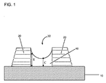
層が液相堆積法によって形成される場合、乾燥フィルムは、フィルム領域にわたって均一な厚さを有していないことが多い。これは、基材における表面不均一性、エッジ効果、未乾燥塗膜にわたる蒸発速度の差異等によって生じる可能性がある。いくつかの実施形態において、電気活性材料は、しばしばウェル構造と称される物理的閉じ込め構造を有する、ワークピース上に液相堆積法によって適用される。乾燥フィルムは、図1に示されているものなど、不均一な厚さを有している可能性がある。追加の層を有していてもよい基材10は、開口部30を画定する20で示されている閉じ込め構造を有する。乾燥電気活性膜が40で示されている。フィルムの厚さは、基材の面に垂直な方向で計測される。Eでの厚さは、Cでの厚さよりかなり厚いことが分かる。電気活性層におけるこのような厚さの不均一性は、素子性能に悪影響を有する可能性がある。OLEDにおいては、発光層における不均一性は、色の変動、低効率および短い耐用年数などの望ましくない影響を生じさせる可能性がある。
少なくとも1つの活性領域を有するワークピースを提供するステップ、
電気活性材料および少なくとも1種の溶剤を含む液体組成物を、前記活性領域においてワークピース上に堆積させて湿潤層を形成するステップ、
ワークピース上の湿潤層を、凝縮器を備える減圧チャンバに入れるステップ、
ワークピース上の湿潤層を、−25℃〜80℃の範囲内の制御温度、および、10-6Torr〜1,000Torrの範囲内の減圧下で、1〜100分間の第1の期間の間処理して部分乾燥層を形成するステップであり、凝縮器は溶剤が適用された減圧で液体として凝縮されることとなる温度で維持されるステップ、
部分乾燥層を、1〜50分間の第2の期間の間100℃を超える温度に加熱して乾燥層を形成するステップ、
を含み、ここで、乾燥層は活性領域において実質的に平坦なプロファイルを有する。
陽極、陰極およびこれらの間に少なくとも1つの電気活性層を備える、少なくとも1つの活性領域を有する電子素子が提供されており、ここで、電気活性層は液相堆積によって形成されており、および、活性領域において実質的に平坦なプロファイルを有する。
この実施例は、凝縮乾燥技術を用いる、実質的に平坦なプロファイルを有する、OLED用途のための電気活性膜の構成を示す。以下の材料を用いた。
緩衝層=緩衝剤1(20nm)、これは、導電性ポリマーおよび高分子フッ素化スルホン酸の水性分散体である。このような材料は、例えば、米国特許出願公開第2004/0102577号明細書、米国特許出願公開第2004/0127637号明細書、および、米国特許出願公開第2005/0205860号明細書に記載されている。
光活性層=13:1ホストH1:ドーパントE1(40nm)。ホストH1はアリール−アントラセン誘導体である。E1はアリールアミン化合物である。このような材料は、例えば、米国特許出願公開第2006/0033421号明細書に記載されている。
陰極=LiF/Al(0.5/100nm)
OLED素子を実施例1と同一の材料を用いて構成した。素子を、印刷後の乾燥ステップ以外は、実施例1と同一の手法を用いて構成した。基材に発光層溶液をノズル印刷した直後、プレートを140℃のホットプレート上に30分間置いた。
Claims (22)
- フィルム形成性材料および少なくとも1種の溶剤を含む液体組成物をワークピース上に堆積させて湿潤層を形成するステップ、
前記ワークピース上の前記湿潤層を、凝縮器を備える減圧チャンバ中に入れるステップ;および
前記湿潤層を、−25°〜80℃の範囲内の制御温度、および、10-6〜1,000Torrの範囲内の適用された減圧下で1〜100分間の間処理するステップ、
を含み、前記凝縮器は、前記溶剤が前記適用された減圧で液体として凝縮されることとなる温度で維持される、減圧乾燥方法。 - 前記凝縮器が表面凝縮器である、請求項1に記載の方法。
- 前記表面凝縮器が、コイルおよびプレートからなる群から選択される、請求項2に記載の方法。
- 前記凝縮器が20℃未満の温度で維持される、請求項1に記載の方法。
- 前記凝縮器が、−15〜15℃の範囲内の温度で維持されている、請求項1に記載の方法。
- 前記減圧チャンバが、凝縮された溶剤を前記チャンバから除去する手段をさらに備える、請求項1に記載の方法。
- 前記溶剤が10-2Torr未満の蒸気圧を有する、請求項1に記載の方法。
- 電気活性材料の層を形成する方法であって、
少なくとも1つの活性領域を有するワークピースを提供するステップ、
前記電気活性材料および少なくとも1種の溶剤を含む液体組成物を、前記活性領域において前記ワークピース上に堆積させて湿潤層を形成するステップ、
前記ワークピース上の前記湿潤層を、凝縮器を備える減圧チャンバに入れるステップ、
前記ワークピース上の前記湿潤層を、−25°〜80℃の範囲内の制御温度、および、10-6〜1,000Torrの範囲内の減圧下で、1〜100分間の第1の期間の間処理して部分乾燥層を形成するステップであり、前記凝縮器は、前記適用された減圧で前記溶剤が液体として凝縮されることとなる温度で維持されるステップ、
前記部分乾燥層を、1〜50分間の第2の期間の間100℃を超える温度に加熱して乾燥層を形成するステップ
を含み、
前記乾燥層は、前記活性領域において実質的に平坦なプロファイルを有する、電気活性材料の層を形成する方法。 - 前記乾燥層が、前記活性領域の90%にわたって+/−10%未満の厚さ変動を有する、請求項8に記載の方法。
- 前記液体組成物が、インクジェット印刷および連続ノズルコーティングからなる群から選択される技術により堆積される、請求項8に記載の方法。
- 前記ワークピースが複数の活性領域を有する、請求項8に記載の方法。
- 前記電気活性材料が、ホスト材料および第1の色に対応する光活性ゲスト材料を含み、および、前記液体組成物が、前記活性領域の第1の部分に堆積される、請求項11に記載の方法。
- 第2のホスト材料および第2の色に対応する第2の光活性ゲスト材料を含む第2の液体組成物が、前記活性領域の第2の部分に堆積される、請求項12に記載の方法。
- 第3のホスト材料および第3の色に対応する第3の光活性ゲスト材料を含む第3の液体組成物が、前記活性領域の第3の部分に堆積される、請求項13に記載の方法。
- 前記凝縮器が表面凝縮器である、請求項8に記載の方法。
- 前記凝縮器が、20℃未満の温度で維持される、請求項8に記載の方法。
- 前記凝縮器が、−15°〜15℃の範囲内の温度で維持されている、請求項8に記載の方法。
- 前記減圧チャンバが、凝縮された溶剤を前記チャンバから除去する手段をさらに備える、請求項8に記載の方法。
- 前記ワークピース上の前記湿潤層が、20〜80℃の範囲内の温度、10-2〜10Torrの範囲内の圧力で、5〜25分間の時間処理される、請求項8に記載の方法。
- 前記ワークピース上の前記湿潤層が、30〜60℃の範囲内の温度、10-2〜1Torrの範囲内の圧力で、5〜15分間の時間の間処理される、請求項8に記載の方法。
- 前記ワークピース上の前記湿潤層が、−25°〜10℃の範囲内の温度、1〜1000Torrの範囲内の圧力で、5〜25分間の時間の間処理される、請求項8に記載の方法。
- 前記ワークピース上の前記湿潤層が、−10〜0℃の範囲内の温度、10〜100Torrの範囲内の圧力で、5〜15分間の時間の間処理される、請求項8に記載の方法。
Applications Claiming Priority (3)
| Application Number | Priority Date | Filing Date | Title |
|---|---|---|---|
| US15842209P | 2009-03-09 | 2009-03-09 | |
| US61/158,422 | 2009-03-09 | ||
| PCT/US2010/026658 WO2010104852A2 (en) | 2009-03-09 | 2010-03-09 | Process for forming an electroactive layer |
Publications (2)
| Publication Number | Publication Date |
|---|---|
| JP2012519950A true JP2012519950A (ja) | 2012-08-30 |
| JP2012519950A5 JP2012519950A5 (ja) | 2013-03-28 |
Family
ID=42729050
Family Applications (1)
| Application Number | Title | Priority Date | Filing Date |
|---|---|---|---|
| JP2011554120A Pending JP2012519950A (ja) | 2009-03-09 | 2010-03-09 | 電気活性層の形成方法 |
Country Status (7)
| Country | Link |
|---|---|
| US (1) | US9209398B2 (ja) |
| EP (1) | EP2406813A4 (ja) |
| JP (1) | JP2012519950A (ja) |
| KR (1) | KR20110139253A (ja) |
| CN (1) | CN102349132B (ja) |
| TW (1) | TW201114082A (ja) |
| WO (1) | WO2010104852A2 (ja) |
Cited By (1)
| Publication number | Priority date | Publication date | Assignee | Title |
|---|---|---|---|---|
| JP2012519981A (ja) * | 2009-03-09 | 2012-08-30 | イー・アイ・デュポン・ドウ・ヌムール・アンド・カンパニー | 電気活性層の形成方法 |
Families Citing this family (10)
| Publication number | Priority date | Publication date | Assignee | Title |
|---|---|---|---|---|
| US10434804B2 (en) | 2008-06-13 | 2019-10-08 | Kateeva, Inc. | Low particle gas enclosure systems and methods |
| WO2010102272A2 (en) * | 2009-03-06 | 2010-09-10 | E. I. Du Pont De Nemours And Company | Process for forming an electroactive layer |
| TWI444602B (zh) * | 2011-04-15 | 2014-07-11 | Univ Chang Gung | A fluorescent powder coating apparatus and a method for detecting white light color temperature in a process immediately |
| JP6392874B2 (ja) | 2013-12-26 | 2018-09-19 | カティーバ, インコーポレイテッド | 電子デバイスの熱処理のための装置および技法 |
| KR101813828B1 (ko) | 2014-01-21 | 2017-12-29 | 카티바, 인크. | 전자 장치 인캡슐레이션을 위한 기기 및 기술 |
| KR101963489B1 (ko) | 2014-04-30 | 2019-07-31 | 카티바, 인크. | 가스 쿠션 장비 및 기판 코팅 기술 |
| JP2019505750A (ja) * | 2015-11-16 | 2019-02-28 | カティーバ, インコーポレイテッド | 基板の熱処理のためのシステムおよび方法 |
| CN107940904B (zh) * | 2017-11-14 | 2019-12-03 | 合肥鑫晟光电科技有限公司 | 一种真空干燥腔室及真空干燥装置 |
| KR102645467B1 (ko) * | 2018-10-18 | 2024-03-11 | 삼성디스플레이 주식회사 | 표시장치의 제조방법 |
| CN111509144B (zh) * | 2020-04-24 | 2022-09-30 | 合肥京东方卓印科技有限公司 | Oled器件的制备方法及显示面板的制备方法 |
Citations (4)
| Publication number | Priority date | Publication date | Assignee | Title |
|---|---|---|---|---|
| JPH11511546A (ja) * | 1995-09-18 | 1999-10-05 | ミネソタ・マイニング・アンド・マニュファクチャリング・カンパニー | 被覆基材乾燥システム |
| JP2000173771A (ja) * | 1998-12-10 | 2000-06-23 | Sharp Corp | ライン光源及びその製造方法 |
| JP2008084566A (ja) * | 2006-09-26 | 2008-04-10 | Toppan Printing Co Ltd | 有機機能性素子の製造方法 |
| JP2008171580A (ja) * | 2007-01-09 | 2008-07-24 | Dainippon Printing Co Ltd | 有機発光素子、有機発光トランジスタ及び発光表示装置 |
Family Cites Families (67)
| Publication number | Priority date | Publication date | Assignee | Title |
|---|---|---|---|---|
| US3630660A (en) * | 1968-10-31 | 1971-12-28 | Burlington Industries Inc | Process for removal of moisture and/or solvents from textile materials |
| US4421781A (en) | 1982-03-29 | 1983-12-20 | Tri/Valley Growers | Continuous vacuum curing and solvent recovery coating process |
| US5199187A (en) * | 1991-07-31 | 1993-04-06 | Sp Industries | Freeze dryer apparatus having an interim condensing system and use thereof |
| US5744009A (en) * | 1995-07-07 | 1998-04-28 | The M. W. Kellogg Company | Method and apparatus for recovering condensables in vapor from a urea vacuum evaporator |
| US5694701A (en) | 1996-09-04 | 1997-12-09 | Minnesota Mining And Manufacturing Company | Coated substrate drying system |
| US5813133A (en) | 1996-09-04 | 1998-09-29 | Minnesota Mining And Manufacturing Company | Coated substrate drying system with magnetic particle orientation |
| JP3899566B2 (ja) | 1996-11-25 | 2007-03-28 | セイコーエプソン株式会社 | 有機el表示装置の製造方法 |
| US6303238B1 (en) | 1997-12-01 | 2001-10-16 | The Trustees Of Princeton University | OLEDs doped with phosphorescent compounds |
| AU9451098A (en) | 1997-10-14 | 1999-05-03 | Patterning Technologies Limited | Method of forming an electronic device |
| JP3417464B2 (ja) | 1998-06-24 | 2003-06-16 | 東京応化工業株式会社 | 平坦化膜形成用塗布液 |
| JP2000056474A (ja) * | 1998-08-05 | 2000-02-25 | Tokyo Electron Ltd | 基板処理方法 |
| US6630274B1 (en) | 1998-12-21 | 2003-10-07 | Seiko Epson Corporation | Color filter and manufacturing method therefor |
| KR100913568B1 (ko) | 1999-05-13 | 2009-08-26 | 더 트러스티즈 오브 프린스턴 유니버시티 | 전계인광에 기초한 고 효율의 유기 발광장치 |
| EP3379591A1 (en) | 1999-12-01 | 2018-09-26 | The Trustees of Princeton University | Complexes of form l2mx |
| US6670645B2 (en) | 2000-06-30 | 2003-12-30 | E. I. Du Pont De Nemours And Company | Electroluminescent iridium compounds with fluorinated phenylpyridines, phenylpyrimidines, and phenylquinolines and devices made with such compounds |
| JP3628997B2 (ja) | 2000-11-27 | 2005-03-16 | セイコーエプソン株式会社 | 有機エレクトロルミネッセンス装置の製造方法 |
| JP4285264B2 (ja) | 2000-11-28 | 2009-06-24 | セイコーエプソン株式会社 | 有機エレクトロルミネッセンス装置の製造方法 |
| JP4021177B2 (ja) | 2000-11-28 | 2007-12-12 | セイコーエプソン株式会社 | 有機エレクトロルミネッセンス装置の製造方法および有機エレクトロルミネッセンス装置並びに電子機器 |
| TW533446B (en) | 2000-12-22 | 2003-05-21 | Koninkl Philips Electronics Nv | Electroluminescent device and a method of manufacturing thereof |
| US6875523B2 (en) | 2001-07-05 | 2005-04-05 | E. I. Du Pont De Nemours And Company | Photoactive lanthanide complexes with phosphine oxides, phosphine oxide-sulfides, pyridine N-oxides, and phosphine oxide-pyridine N-oxides, and devices made with such complexes |
| KR20040018467A (ko) | 2001-07-18 | 2004-03-03 | 이 아이 듀폰 디 네모아 앤드 캄파니 | 이민 리간드와의 발광 란탄족 착물 및 이러한 착물을사용하여 제조된 장치 |
| JP2003133691A (ja) | 2001-10-22 | 2003-05-09 | Seiko Epson Corp | 膜パターンの形成方法、膜パターン形成装置、導電膜配線、電気光学装置、電子機器、並びに非接触型カード媒体 |
| US7166368B2 (en) | 2001-11-07 | 2007-01-23 | E. I. Du Pont De Nemours And Company | Electroluminescent platinum compounds and devices made with such compounds |
| JP4164256B2 (ja) | 2001-11-27 | 2008-10-15 | 東京エレクトロン株式会社 | 減圧乾燥装置及び減圧乾燥方法 |
| EP2306788A1 (en) | 2001-12-26 | 2011-04-06 | E. I. du Pont de Nemours and Company | Iridium compounds and devices made therewith |
| US6858464B2 (en) | 2002-06-19 | 2005-02-22 | Semiconductor Energy Laboratory Co., Ltd. | Method of manufacturing light emitting device |
| US6713339B2 (en) | 2002-06-21 | 2004-03-30 | Micron Technology, Inc. | Methods of forming switchable circuit devices |
| KR101018547B1 (ko) | 2002-07-19 | 2011-03-03 | 이데미쓰 고산 가부시키가이샤 | 유기 전기발광 소자 및 유기 발광 매체 |
| JP4239560B2 (ja) | 2002-08-02 | 2009-03-18 | セイコーエプソン株式会社 | 組成物とこれを用いた有機導電性膜の製造方法 |
| US6963005B2 (en) | 2002-08-15 | 2005-11-08 | E. I. Du Pont De Nemours And Company | Compounds comprising phosphorus-containing metal complexes |
| CA2499364A1 (en) | 2002-09-24 | 2004-04-08 | E. I. Du Pont De Nemours And Company | Water dispersible polyanilines made with polymeric acid colloids for electronics applications |
| WO2004029128A2 (en) | 2002-09-24 | 2004-04-08 | E.I. Du Pont De Nemours And Company | Water dispersible polythiophenes made with polymeric acid colloids |
| JP2004223354A (ja) | 2003-01-21 | 2004-08-12 | Seiko Epson Corp | 液状組成物の塗布方法、el素子の製造方法、カラーフィルタの製造方法、電気光学装置、電子機器 |
| JP2004351272A (ja) | 2003-05-27 | 2004-12-16 | Seiko Epson Corp | 薄膜パターンの形成方法及びデバイスの製造方法、電気光学装置及び電子機器 |
| US6867081B2 (en) | 2003-07-31 | 2005-03-15 | Hewlett-Packard Development Company, L.P. | Solution-processed thin film transistor formation method |
| TWI365218B (en) | 2003-11-17 | 2012-06-01 | Sumitomo Chemical Co | Conjugated oligomers or polymers based on crosslinkable arylamine compounds |
| JP2005158824A (ja) * | 2003-11-20 | 2005-06-16 | Seiko Epson Corp | 成膜方法、膜、電子デバイスおよび電子機器 |
| JP2005172316A (ja) | 2003-12-09 | 2005-06-30 | Seiko Epson Corp | 減圧乾燥装置、電気光学装置、電気光学装置の製造方法および電子機器 |
| US20050129843A1 (en) | 2003-12-11 | 2005-06-16 | Xerox Corporation | Nanoparticle deposition process |
| JP2005235852A (ja) | 2004-02-17 | 2005-09-02 | Seiko Epson Corp | 多層膜の形成方法及びデバイスの製造方法 |
| US7351358B2 (en) | 2004-03-17 | 2008-04-01 | E.I. Du Pont De Nemours And Company | Water dispersible polypyrroles made with polymeric acid colloids for electronics applications |
| JP4055171B2 (ja) | 2004-05-19 | 2008-03-05 | セイコーエプソン株式会社 | カラーフィルタ基板の製造方法、電気光学装置の製造方法、電気光学装置、電子機器 |
| US7023013B2 (en) | 2004-06-16 | 2006-04-04 | Eastman Kodak Company | Array of light-emitting OLED microcavity pixels |
| US7807741B2 (en) | 2004-06-17 | 2010-10-05 | Sharp Kabushiki Kaisha | Coating liquid, film production method, production method of functional device, and functional device |
| US8158517B2 (en) | 2004-06-28 | 2012-04-17 | Semiconductor Energy Laboratory Co., Ltd. | Method for manufacturing wiring substrate, thin film transistor, display device and television device |
| GB2416428A (en) * | 2004-07-19 | 2006-01-25 | Seiko Epson Corp | Method for fabricating a semiconductor element from a dispersion of semiconductor particles |
| JP4148933B2 (ja) | 2004-08-31 | 2008-09-10 | シャープ株式会社 | 機能膜の製造方法、機能膜形成用塗液、機能素子、電子デバイス及び表示装置 |
| US7217583B2 (en) * | 2004-09-21 | 2007-05-15 | Cree, Inc. | Methods of coating semiconductor light emitting elements by evaporating solvent from a suspension |
| TWI247111B (en) | 2004-09-22 | 2006-01-11 | Chunghwa Picture Tubes Ltd | Method of detecting foreign objects in display manufacture processes |
| US7268006B2 (en) | 2004-12-30 | 2007-09-11 | E.I. Du Pont De Nemours And Company | Electronic device including a guest material within a layer and a process for forming the same |
| JP5082189B2 (ja) | 2005-01-14 | 2012-11-28 | 大日本印刷株式会社 | コーティング液、金属酸化物膜およびその形成方法 |
| JP4876415B2 (ja) * | 2005-03-29 | 2012-02-15 | セイコーエプソン株式会社 | 有機el装置の製造方法、デバイスの製造方法 |
| KR100663076B1 (ko) | 2005-08-31 | 2007-01-02 | 한국과학기술원 | 반도체 기판 상의 소정 영역에 탄소나노튜브를 형성시키는 방법, 이를 이용한 반도체 도선 형성방법 및 이를 이용하여 인덕터 소자 제조 방법 |
| JP2007123257A (ja) | 2005-09-27 | 2007-05-17 | Mitsubishi Chemicals Corp | 有機電界発光素子の製造方法 |
| JP4396607B2 (ja) * | 2005-09-28 | 2010-01-13 | セイコーエプソン株式会社 | 膜形成方法、有機エレクトロルミネセンス装置の製造方法、有機エレクトロルミネセンス装置及び電子機器 |
| KR101211836B1 (ko) | 2005-10-24 | 2012-12-12 | 삼성코닝정밀소재 주식회사 | 다공성 칼코게나이드 박막, 그 제조방법 및 이를 채용한전자소자 |
| KR100643376B1 (ko) | 2005-10-24 | 2006-11-10 | 삼성전자주식회사 | 표시장치와 표시장치의 제조방법 |
| US8124172B2 (en) | 2006-03-02 | 2012-02-28 | E.I. Du Pont De Nemours And Company | Process for making contained layers and devices made with same |
| US20070278936A1 (en) | 2006-06-02 | 2007-12-06 | Norman Herron | Red emitter complexes of IR(III) and devices made with such compounds |
| WO2007145979A2 (en) | 2006-06-05 | 2007-12-21 | E. I. Du Pont De Nemours And Company | Liquid composition for deposition of organic active materials in the field of oled printing |
| US7491646B2 (en) | 2006-07-20 | 2009-02-17 | Xerox Corporation | Electrically conductive feature fabrication process |
| WO2008024378A2 (en) | 2006-08-24 | 2008-02-28 | E. I. Du Pont De Nemours And Company | Hole transport polymers |
| JP4560577B2 (ja) | 2006-10-18 | 2010-10-13 | パナソニック株式会社 | 多層情報記録媒体の製造方法、多層情報記録媒体の製造装置、および多層情報記録媒体 |
| DE102006054481A1 (de) * | 2006-11-18 | 2008-05-21 | Eppendorf Ag | Vakuumkonzentrator und Verfahren zur Vakuumkonzentration |
| US20080289676A1 (en) | 2007-05-25 | 2008-11-27 | Guidotti Ronald Armand | Electrode for a thermal battery and method of making the same |
| CN101275282B (zh) | 2007-12-26 | 2011-06-08 | 中国核动力研究设计院 | 超晶格热电材料的制备方法 |
| GB0803950D0 (en) * | 2008-03-03 | 2008-04-09 | Cambridge Display Technology O | Solvent for printing composition |
-
2010
- 2010-03-09 KR KR1020117023585A patent/KR20110139253A/ko active Search and Examination
- 2010-03-09 TW TW099106806A patent/TW201114082A/zh unknown
- 2010-03-09 EP EP10751285A patent/EP2406813A4/en not_active Withdrawn
- 2010-03-09 JP JP2011554120A patent/JP2012519950A/ja active Pending
- 2010-03-09 US US13/203,279 patent/US9209398B2/en active Active
- 2010-03-09 CN CN201080012033.8A patent/CN102349132B/zh active Active
- 2010-03-09 WO PCT/US2010/026658 patent/WO2010104852A2/en active Application Filing
Patent Citations (4)
| Publication number | Priority date | Publication date | Assignee | Title |
|---|---|---|---|---|
| JPH11511546A (ja) * | 1995-09-18 | 1999-10-05 | ミネソタ・マイニング・アンド・マニュファクチャリング・カンパニー | 被覆基材乾燥システム |
| JP2000173771A (ja) * | 1998-12-10 | 2000-06-23 | Sharp Corp | ライン光源及びその製造方法 |
| JP2008084566A (ja) * | 2006-09-26 | 2008-04-10 | Toppan Printing Co Ltd | 有機機能性素子の製造方法 |
| JP2008171580A (ja) * | 2007-01-09 | 2008-07-24 | Dainippon Printing Co Ltd | 有機発光素子、有機発光トランジスタ及び発光表示装置 |
Cited By (1)
| Publication number | Priority date | Publication date | Assignee | Title |
|---|---|---|---|---|
| JP2012519981A (ja) * | 2009-03-09 | 2012-08-30 | イー・アイ・デュポン・ドウ・ヌムール・アンド・カンパニー | 電気活性層の形成方法 |
Also Published As
| Publication number | Publication date |
|---|---|
| WO2010104852A2 (en) | 2010-09-16 |
| US20110305824A1 (en) | 2011-12-15 |
| EP2406813A4 (en) | 2012-07-25 |
| WO2010104852A3 (en) | 2011-01-27 |
| TW201114082A (en) | 2011-04-16 |
| CN102349132A (zh) | 2012-02-08 |
| US9209398B2 (en) | 2015-12-08 |
| KR20110139253A (ko) | 2011-12-28 |
| CN102349132B (zh) | 2014-09-17 |
| EP2406813A2 (en) | 2012-01-18 |
Similar Documents
| Publication | Publication Date | Title |
|---|---|---|
| US9209398B2 (en) | Process for forming an electroactive layer | |
| US8907353B2 (en) | Process for forming an electroactive layer | |
| US9306185B2 (en) | Process and materials for making contained layers and devices made with same | |
| JP2015062900A (ja) | 電気活性層の形成方法 | |
| JP2011501470A (ja) | 電子輸送二重層およびそのような二重層から製造したデバイス | |
| JP5701782B2 (ja) | 電気活性層の形成方法 | |
| US20130087779A1 (en) | Process and materials for making contained layers and devices made with same | |
| JP5258302B2 (ja) | 有機電子デバイスおよび方法 | |
| US20070096086A1 (en) | Hole injection electrode |
Legal Events
| Date | Code | Title | Description |
|---|---|---|---|
| A521 | Request for written amendment filed |
Free format text: JAPANESE INTERMEDIATE CODE: A523 Effective date: 20130205 |
|
| A621 | Written request for application examination |
Free format text: JAPANESE INTERMEDIATE CODE: A621 Effective date: 20130205 |
|
| A977 | Report on retrieval |
Free format text: JAPANESE INTERMEDIATE CODE: A971007 Effective date: 20130930 |
|
| A131 | Notification of reasons for refusal |
Free format text: JAPANESE INTERMEDIATE CODE: A131 Effective date: 20131126 |
|
| A521 | Request for written amendment filed |
Free format text: JAPANESE INTERMEDIATE CODE: A523 Effective date: 20140220 |
|
| A131 | Notification of reasons for refusal |
Free format text: JAPANESE INTERMEDIATE CODE: A131 Effective date: 20140819 |
|
| A521 | Request for written amendment filed |
Free format text: JAPANESE INTERMEDIATE CODE: A523 Effective date: 20141114 |
|
| A02 | Decision of refusal |
Free format text: JAPANESE INTERMEDIATE CODE: A02 Effective date: 20150106 |