JP2012519941A - 電気活性層の形成方法 - Google Patents
電気活性層の形成方法 Download PDFInfo
- Publication number
- JP2012519941A JP2012519941A JP2011553161A JP2011553161A JP2012519941A JP 2012519941 A JP2012519941 A JP 2012519941A JP 2011553161 A JP2011553161 A JP 2011553161A JP 2011553161 A JP2011553161 A JP 2011553161A JP 2012519941 A JP2012519941 A JP 2012519941A
- Authority
- JP
- Japan
- Prior art keywords
- layer
- electroactive
- range
- workpiece
- active region
- Prior art date
- Legal status (The legal status is an assumption and is not a legal conclusion. Google has not performed a legal analysis and makes no representation as to the accuracy of the status listed.)
- Pending
Links
Images


Classifications
-
- F—MECHANICAL ENGINEERING; LIGHTING; HEATING; WEAPONS; BLASTING
- F26—DRYING
- F26B—DRYING SOLID MATERIALS OR OBJECTS BY REMOVING LIQUID THEREFROM
- F26B5/00—Drying solid materials or objects by processes not involving the application of heat
- F26B5/04—Drying solid materials or objects by processes not involving the application of heat by evaporation or sublimation of moisture under reduced pressure, e.g. in a vacuum
-
- F—MECHANICAL ENGINEERING; LIGHTING; HEATING; WEAPONS; BLASTING
- F26—DRYING
- F26B—DRYING SOLID MATERIALS OR OBJECTS BY REMOVING LIQUID THEREFROM
- F26B21/00—Arrangements or duct systems, e.g. in combination with pallet boxes, for supplying and controlling air or gases for drying solid materials or objects
- F26B21/06—Controlling, e.g. regulating, parameters of gas supply
- F26B21/08—Humidity
- F26B21/083—Humidity by using sorbent or hygroscopic materials, e.g. chemical substances, molecular sieves
-
- H—ELECTRICITY
- H10—SEMICONDUCTOR DEVICES; ELECTRIC SOLID-STATE DEVICES NOT OTHERWISE PROVIDED FOR
- H10K—ORGANIC ELECTRIC SOLID-STATE DEVICES
- H10K10/00—Organic devices specially adapted for rectifying, amplifying, oscillating or switching; Organic capacitors or resistors having a potential-jump barrier or a surface barrier
-
- H—ELECTRICITY
- H10—SEMICONDUCTOR DEVICES; ELECTRIC SOLID-STATE DEVICES NOT OTHERWISE PROVIDED FOR
- H10K—ORGANIC ELECTRIC SOLID-STATE DEVICES
- H10K30/00—Organic devices sensitive to infrared radiation, light, electromagnetic radiation of shorter wavelength or corpuscular radiation
-
- H—ELECTRICITY
- H10—SEMICONDUCTOR DEVICES; ELECTRIC SOLID-STATE DEVICES NOT OTHERWISE PROVIDED FOR
- H10K—ORGANIC ELECTRIC SOLID-STATE DEVICES
- H10K50/00—Organic light-emitting devices
-
- H—ELECTRICITY
- H10—SEMICONDUCTOR DEVICES; ELECTRIC SOLID-STATE DEVICES NOT OTHERWISE PROVIDED FOR
- H10K—ORGANIC ELECTRIC SOLID-STATE DEVICES
- H10K71/00—Manufacture or treatment specially adapted for the organic devices covered by this subclass
-
- H—ELECTRICITY
- H10—SEMICONDUCTOR DEVICES; ELECTRIC SOLID-STATE DEVICES NOT OTHERWISE PROVIDED FOR
- H10K—ORGANIC ELECTRIC SOLID-STATE DEVICES
- H10K71/00—Manufacture or treatment specially adapted for the organic devices covered by this subclass
- H10K71/10—Deposition of organic active material
- H10K71/12—Deposition of organic active material using liquid deposition, e.g. spin coating
- H10K71/13—Deposition of organic active material using liquid deposition, e.g. spin coating using printing techniques, e.g. ink-jet printing or screen printing
- H10K71/135—Deposition of organic active material using liquid deposition, e.g. spin coating using printing techniques, e.g. ink-jet printing or screen printing using ink-jet printing
-
- H—ELECTRICITY
- H10—SEMICONDUCTOR DEVICES; ELECTRIC SOLID-STATE DEVICES NOT OTHERWISE PROVIDED FOR
- H10K—ORGANIC ELECTRIC SOLID-STATE DEVICES
- H10K71/00—Manufacture or treatment specially adapted for the organic devices covered by this subclass
- H10K71/40—Thermal treatment, e.g. annealing in the presence of a solvent vapour
-
- H—ELECTRICITY
- H10—SEMICONDUCTOR DEVICES; ELECTRIC SOLID-STATE DEVICES NOT OTHERWISE PROVIDED FOR
- H10K—ORGANIC ELECTRIC SOLID-STATE DEVICES
- H10K71/00—Manufacture or treatment specially adapted for the organic devices covered by this subclass
- H10K71/811—Controlling the atmosphere during processing
-
- H—ELECTRICITY
- H10—SEMICONDUCTOR DEVICES; ELECTRIC SOLID-STATE DEVICES NOT OTHERWISE PROVIDED FOR
- H10K—ORGANIC ELECTRIC SOLID-STATE DEVICES
- H10K50/00—Organic light-emitting devices
- H10K50/10—OLEDs or polymer light-emitting diodes [PLED]
- H10K50/11—OLEDs or polymer light-emitting diodes [PLED] characterised by the electroluminescent [EL] layers
-
- H—ELECTRICITY
- H10—SEMICONDUCTOR DEVICES; ELECTRIC SOLID-STATE DEVICES NOT OTHERWISE PROVIDED FOR
- H10K—ORGANIC ELECTRIC SOLID-STATE DEVICES
- H10K50/00—Organic light-emitting devices
- H10K50/10—OLEDs or polymer light-emitting diodes [PLED]
- H10K50/14—Carrier transporting layers
-
- H—ELECTRICITY
- H10—SEMICONDUCTOR DEVICES; ELECTRIC SOLID-STATE DEVICES NOT OTHERWISE PROVIDED FOR
- H10K—ORGANIC ELECTRIC SOLID-STATE DEVICES
- H10K50/00—Organic light-emitting devices
- H10K50/10—OLEDs or polymer light-emitting diodes [PLED]
- H10K50/17—Carrier injection layers
-
- H—ELECTRICITY
- H10—SEMICONDUCTOR DEVICES; ELECTRIC SOLID-STATE DEVICES NOT OTHERWISE PROVIDED FOR
- H10K—ORGANIC ELECTRIC SOLID-STATE DEVICES
- H10K59/00—Integrated devices, or assemblies of multiple devices, comprising at least one organic light-emitting element covered by group H10K50/00
- H10K59/10—OLED displays
- H10K59/12—Active-matrix OLED [AMOLED] displays
- H10K59/122—Pixel-defining structures or layers, e.g. banks
-
- H—ELECTRICITY
- H10—SEMICONDUCTOR DEVICES; ELECTRIC SOLID-STATE DEVICES NOT OTHERWISE PROVIDED FOR
- H10K—ORGANIC ELECTRIC SOLID-STATE DEVICES
- H10K59/00—Integrated devices, or assemblies of multiple devices, comprising at least one organic light-emitting element covered by group H10K50/00
- H10K59/10—OLED displays
- H10K59/17—Passive-matrix OLED displays
- H10K59/173—Passive-matrix OLED displays comprising banks or shadow masks
-
- H—ELECTRICITY
- H10—SEMICONDUCTOR DEVICES; ELECTRIC SOLID-STATE DEVICES NOT OTHERWISE PROVIDED FOR
- H10K—ORGANIC ELECTRIC SOLID-STATE DEVICES
- H10K59/00—Integrated devices, or assemblies of multiple devices, comprising at least one organic light-emitting element covered by group H10K50/00
- H10K59/30—Devices specially adapted for multicolour light emission
- H10K59/35—Devices specially adapted for multicolour light emission comprising red-green-blue [RGB] subpixels
-
- H—ELECTRICITY
- H10—SEMICONDUCTOR DEVICES; ELECTRIC SOLID-STATE DEVICES NOT OTHERWISE PROVIDED FOR
- H10K—ORGANIC ELECTRIC SOLID-STATE DEVICES
- H10K85/00—Organic materials used in the body or electrodes of devices covered by this subclass
- H10K85/60—Organic compounds having low molecular weight
- H10K85/615—Polycyclic condensed aromatic hydrocarbons, e.g. anthracene
-
- H—ELECTRICITY
- H10—SEMICONDUCTOR DEVICES; ELECTRIC SOLID-STATE DEVICES NOT OTHERWISE PROVIDED FOR
- H10K—ORGANIC ELECTRIC SOLID-STATE DEVICES
- H10K85/00—Organic materials used in the body or electrodes of devices covered by this subclass
- H10K85/60—Organic compounds having low molecular weight
- H10K85/631—Amine compounds having at least two aryl rest on at least one amine-nitrogen atom, e.g. triphenylamine
-
- Y—GENERAL TAGGING OF NEW TECHNOLOGICAL DEVELOPMENTS; GENERAL TAGGING OF CROSS-SECTIONAL TECHNOLOGIES SPANNING OVER SEVERAL SECTIONS OF THE IPC; TECHNICAL SUBJECTS COVERED BY FORMER USPC CROSS-REFERENCE ART COLLECTIONS [XRACs] AND DIGESTS
- Y02—TECHNOLOGIES OR APPLICATIONS FOR MITIGATION OR ADAPTATION AGAINST CLIMATE CHANGE
- Y02E—REDUCTION OF GREENHOUSE GAS [GHG] EMISSIONS, RELATED TO ENERGY GENERATION, TRANSMISSION OR DISTRIBUTION
- Y02E10/00—Energy generation through renewable energy sources
- Y02E10/50—Photovoltaic [PV] energy
- Y02E10/549—Organic PV cells
Landscapes
- Engineering & Computer Science (AREA)
- Manufacturing & Machinery (AREA)
- Mechanical Engineering (AREA)
- General Engineering & Computer Science (AREA)
- Molecular Biology (AREA)
- Health & Medical Sciences (AREA)
- Life Sciences & Earth Sciences (AREA)
- Physics & Mathematics (AREA)
- Chemical Kinetics & Catalysis (AREA)
- General Chemical & Material Sciences (AREA)
- Chemical & Material Sciences (AREA)
- Optics & Photonics (AREA)
- Electromagnetism (AREA)
- Electroluminescent Light Sources (AREA)
- Application Of Or Painting With Fluid Materials (AREA)
Abstract
Description
本出願は、その全体が参照により援用されている、2009年3月6日に出願の米国仮特許出願第61/158,094号明細書に基づく、米国特許法第119条(e)の優先権を主張する。
少なくとも1つの活性領域を有するワークピースを提供するステップ、
電気活性材料を含む液体組成物を活性領域におけるワークピース上に堆積させて、湿潤層を形成するステップ、
ワークピース上の湿潤層を、−25℃〜80℃の範囲内の制御温度、および、10-6Torr〜1,000Torrの範囲内の減圧下で、1〜100分間の第1の期間の間処理して、部分乾燥層を形成するステップ、
部分乾燥層を、1〜50分間の第2の期間の間100℃を超える温度に加熱して乾燥層を形成するステップ、
を含み、ここで、乾燥層は、活性領域において実質的に平坦なプロファイルを有する。
以下に記載されている実施形態の詳細に入る前に、いくつかの用語が定義または明確化されている。
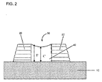
層が液相堆積法によって形成される場合、乾燥フィルムは、フィルム領域にわたって均一な厚さを有していないことが多い。これは、基材における表面不均一性、エッジ効果、未乾燥塗膜にわたる蒸発速度の差異等によって生じる可能性がある。いくつかの実施形態において、電気活性材料は、しばしばウェル構造と称される物理的閉じ込め構造を有する、ワークピース上に液相堆積法によって適用される。乾燥フィルムは、図1に示されているものなど、不均一な厚さを有している可能性がある。追加の層を有していてもよい基材10は、開口部30を画定する20で示されている閉じ込め構造を有する。乾燥電気活性膜が40で示されている。フィルムの厚さは、基材の面に垂直な方向で計測される。Eでの厚さは、Cでの厚さよりかなり厚いことが分かる。電気活性層におけるこのような厚さの不均一性は、素子性能に悪影響を有する可能性がある。OLEDにおいては、発光層における不均一性は、色の変動、低効率および短い耐用年数などの望ましくない影響を生じさせる可能性がある。
少なくとも1つの活性領域を有するワークピースを提供するステップ、
電気活性材料を含む液体組成物を活性領域におけるワークピース上に堆積させて湿潤層を形成するステップ、
ワークピース上の湿潤層を、−25℃〜80℃の範囲内の制御温度、および、10-6Torr〜1,000Torrの範囲内の減圧下で、1〜100分間の第1の期間の間処理して、部分乾燥層を形成するステップ、
部分乾燥層を、1〜50分間の第2の期間の間100℃を超える温度に加熱して乾燥層を形成するステップ、
を順番に含み、乾燥層は、活性領域において実質的に平坦なプロファイルを有する。
陽極、陰極およびこれらの間に少なくとも1つの電気活性層を備える、少なくとも1つの活性領域を有する電子素子が提供されており、ここで、電気活性層は液相堆積によって形成されており、および、活性領域において実質的に平坦なプロファイルを有する。
この実施例は、実質的に平坦なプロファイルを有する、OLED用途のための電気活性膜の構成を示す。以下の材料を用いた。
緩衝層=緩衝剤1(20nm)、これは、導電性ポリマーおよび高分子フッ素化スルホン酸の水性分散体である。このような材料は、例えば、米国特許出願公開第2004/0102577号明細書、米国特許出願公開第2004/0127637号明細書、および、米国特許出願公開第2005/0205860号明細書に記載されている。
陰極=LiF/Al(0.5/100nm)
この実施例は、乾燥ステップにおいてターボ分子ポンプを用いる、実質的に平坦なプロファイルを有する、OLED用途のための電気活性膜の構成を示す。以下の材料を用いた。
緩衝層=緩衝剤1(20nm)
正孔輸送層=HT−2(20nm)、これはアリールアミン含有ポリマーである
光活性層=13:1ホストH1:ドーパントE2(40nm)。E2は、例えば、米国特許出願公開第2006/0033421号明細書に記載のアリールアミン化合物である。
陰極=LiF/Al(0.5/100nm)
OLED素子を実施例2と同一の材料を用いて構成した。素子を、印刷後の乾燥ステップ以外は、実施例2と同一の手法を用いて構成した。基材に発光層溶液をノズル印刷した直後、プレートを140℃のホットプレート上に30分間置いた。
Claims (22)
- 少なくとも1つの活性領域を有するワークピースを提供するステップ、
電気活性材料を含む液体組成物を前記ワークピースにおける前記活性領域上に堆積させて湿潤層を形成するステップ、
前記ワークピース上の前記湿潤層を、−25〜80℃の範囲内の制御温度、および、10-6〜1,000Torrの範囲内の減圧下で、1〜100分間の第1の期間の間処理して、部分乾燥層を形成するステップ、
前記部分乾燥層を、1〜50分間の第2の期間の間100℃を超える温度に加熱して乾燥層を形成するステップ、
を含み、前記乾燥層は、前記活性領域において実質的に平坦なプロファイルを有する、電気活性材料の層を形成する方法。 - 前記乾燥層が、前記活性領域の90%にわたって+/−10%未満の厚さ変動を有する、請求項1に記載の方法。
- 前記液体組成物が、インクジェット印刷および連続ノズルコーティングからなる群から選択される技術により堆積される、請求項1に記載の方法。
- 前記ワークピースが複数の活性領域を有する、請求項1に記載の方法。
- 前記電気活性材料が、ホスト材料および第1の色に対応する光活性ゲスト材料を含んでおり、および、前記液体組成物が、前記活性領域の第1の部分に堆積される、請求項4に記載の方法。
- 第2のホスト材料および第2の色に対応する第2の光活性ゲスト材料を含む第2の液体組成物が、前記活性領域の第2の部分に堆積される、請求項5に記載の方法。
- 第3のホスト材料および第3の色に対応する第3の光活性ゲスト材料を含む第3の液体組成物が、前記活性領域の第3の部分に堆積される、請求項6に記載の方法。
- 前記電気活性材料が正孔注入材料から本質的に構成される、請求項1に記載の方法。
- 前記電気活性材料が正孔輸送材料から本質的に構成される、請求項1に記載の方法。
- 前記ワークピース上の前記湿潤層が、20〜80℃の範囲内の温度、10-2〜10Torrの範囲内の圧力で、5〜25分間の時間の間処理される、請求項1に記載の方法。
- 前記ワークピース上の前記湿潤層が、30〜60℃の範囲内の温度、10-2〜1Torrの範囲内の圧力で、5〜15分間の時間の間処理される、請求項1に記載の方法。
- 前記ワークピース上の前記湿潤層が、−25〜10℃の範囲内の温度、1〜1000Torrの範囲内の圧力で、5〜25分間の時間の間処理される、請求項1に記載の方法。
- 前記ワークピース上の前記湿潤層が、−10〜0℃の範囲内の温度、10〜100Torrの範囲内の圧力で、5〜15分間の時間の間処理される、請求項1に記載の方法。
- 前記減圧が、10-4〜10-6Torrの範囲内である、請求項1に記載の方法。
- 前記減圧が、乾燥真空ポンプ、ターボポンプ、回転真空ポンプ、油拡散ポンプ、低温ポンプおよび吸着ポンプからなる群から選択されるポンプにより減圧される、請求項14に記載の方法。
- 前記ポンプがターボ分子ポンプである、請求項15に記載の方法。
- 陽極、陰極、および、これらの間の電気活性層を備え、前記電気活性層は、液相堆積により形成され、実質的に平坦なプロファイルを有する、少なくとも1つの活性領域を有する電子素子。
- 前記電気活性層が光活性層である、請求項17に記載の素子。
- 前記電気活性層が発光層である、請求項18に記載の素子。
- 前記電気活性層が正孔輸送層である、請求項17に記載の素子。
- 前記電気活性層が正孔注入層である、請求項17に記載の素子。
- 前記活性領域が、物理的閉じ込め構造によってサブピクセル領域に分けられており、前記電気活性層が前記サブピクセル領域中にある、請求項17に記載の素子。
Applications Claiming Priority (3)
| Application Number | Priority Date | Filing Date | Title |
|---|---|---|---|
| US15809409P | 2009-03-06 | 2009-03-06 | |
| US61/158,094 | 2009-03-06 | ||
| PCT/US2010/026467 WO2010102272A2 (en) | 2009-03-06 | 2010-03-08 | Process for forming an electroactive layer |
Related Child Applications (1)
| Application Number | Title | Priority Date | Filing Date |
|---|---|---|---|
| JP2014232460A Division JP2015062900A (ja) | 2009-03-06 | 2014-11-17 | 電気活性層の形成方法 |
Publications (2)
| Publication Number | Publication Date |
|---|---|
| JP2012519941A true JP2012519941A (ja) | 2012-08-30 |
| JP2012519941A5 JP2012519941A5 (ja) | 2014-03-13 |
Family
ID=42710245
Family Applications (2)
| Application Number | Title | Priority Date | Filing Date |
|---|---|---|---|
| JP2011553161A Pending JP2012519941A (ja) | 2009-03-06 | 2010-03-08 | 電気活性層の形成方法 |
| JP2014232460A Pending JP2015062900A (ja) | 2009-03-06 | 2014-11-17 | 電気活性層の形成方法 |
Family Applications After (1)
| Application Number | Title | Priority Date | Filing Date |
|---|---|---|---|
| JP2014232460A Pending JP2015062900A (ja) | 2009-03-06 | 2014-11-17 | 電気活性層の形成方法 |
Country Status (7)
| Country | Link |
|---|---|
| US (2) | US8778708B2 (ja) |
| EP (1) | EP2404315A4 (ja) |
| JP (2) | JP2012519941A (ja) |
| KR (1) | KR20110134452A (ja) |
| CN (1) | CN102318040B (ja) |
| TW (1) | TW201039382A (ja) |
| WO (1) | WO2010102272A2 (ja) |
Cited By (2)
| Publication number | Priority date | Publication date | Assignee | Title |
|---|---|---|---|---|
| JP2014035911A (ja) * | 2012-08-09 | 2014-02-24 | Panasonic Corp | 有機膜の製造方法と有機elパネルの製造方法 |
| JP2015191739A (ja) * | 2014-03-27 | 2015-11-02 | セイコーエプソン株式会社 | 発光素子、発光素子の製造方法、発光装置および電子機器 |
Families Citing this family (6)
| Publication number | Priority date | Publication date | Assignee | Title |
|---|---|---|---|---|
| CN102318040B (zh) * | 2009-03-06 | 2014-09-17 | E.I.内穆尔杜邦公司 | 形成电活性层的方法 |
| KR101952119B1 (ko) * | 2012-05-24 | 2019-02-28 | 삼성전자 주식회사 | 메탈 실리사이드를 포함하는 반도체 장치 및 이의 제조 방법 |
| CN104596205B (zh) * | 2015-02-13 | 2016-08-03 | 京东方科技集团股份有限公司 | 一种真空干燥装置及真空干燥方法 |
| CN105702871B (zh) * | 2016-02-02 | 2020-03-31 | 西安交通大学 | 一种利用溶液抽气通气法制备钙钛矿太阳能电池中钙钛矿薄膜的方法 |
| CN105702870A (zh) * | 2016-02-02 | 2016-06-22 | 西安交通大学 | 一种利用溶液抽气法制备钙钛矿太阳能电池中钙钛矿薄膜的方法 |
| EP3507677B1 (en) * | 2016-08-30 | 2021-09-29 | BOE Technology Group Co., Ltd. | Display panel, display apparatus having the same, and fabricating method thereof |
Citations (2)
| Publication number | Priority date | Publication date | Assignee | Title |
|---|---|---|---|---|
| JP2004140004A (ja) * | 2000-11-28 | 2004-05-13 | Seiko Epson Corp | 有機エレクトロルミネッセンス装置の製造方法および有機エレクトロルミネッセンス装置並びに電子機器 |
| JP2006068598A (ja) * | 2004-08-31 | 2006-03-16 | Sharp Corp | 機能膜の製造方法、機能膜形成用塗液、機能素子、電子デバイス及び表示装置 |
Family Cites Families (82)
| Publication number | Priority date | Publication date | Assignee | Title |
|---|---|---|---|---|
| US3630660A (en) | 1968-10-31 | 1971-12-28 | Burlington Industries Inc | Process for removal of moisture and/or solvents from textile materials |
| US4421781A (en) | 1982-03-29 | 1983-12-20 | Tri/Valley Growers | Continuous vacuum curing and solvent recovery coating process |
| US5199187A (en) | 1991-07-31 | 1993-04-06 | Sp Industries | Freeze dryer apparatus having an interim condensing system and use thereof |
| US5744009A (en) | 1995-07-07 | 1998-04-28 | The M. W. Kellogg Company | Method and apparatus for recovering condensables in vapor from a urea vacuum evaporator |
| US5694701A (en) | 1996-09-04 | 1997-12-09 | Minnesota Mining And Manufacturing Company | Coated substrate drying system |
| BR9610658A (pt) | 1995-09-18 | 1999-02-17 | Minnesota Mining & Mfg | Processo e aparelho para secagem de um substrato revestido |
| US5813133A (en) | 1996-09-04 | 1998-09-29 | Minnesota Mining And Manufacturing Company | Coated substrate drying system with magnetic particle orientation |
| JP3899566B2 (ja) | 1996-11-25 | 2007-03-28 | セイコーエプソン株式会社 | 有機el表示装置の製造方法 |
| US6303238B1 (en) | 1997-12-01 | 2001-10-16 | The Trustees Of Princeton University | OLEDs doped with phosphorescent compounds |
| WO1999019900A2 (en) | 1997-10-14 | 1999-04-22 | Patterning Technologies Limited | Method of forming an electronic device |
| JP3417464B2 (ja) * | 1998-06-24 | 2003-06-16 | 東京応化工業株式会社 | 平坦化膜形成用塗布液 |
| US6630274B1 (en) | 1998-12-21 | 2003-10-07 | Seiko Epson Corporation | Color filter and manufacturing method therefor |
| EP3321954A1 (en) | 1999-05-13 | 2018-05-16 | The Trustees of Princeton University | Very high efficiency organic light emitting devices based on electrophosphorescence |
| EP1933395B2 (en) | 1999-12-01 | 2019-08-07 | The Trustees of Princeton University | Complexes of form L2IrX |
| US6936485B2 (en) * | 2000-03-27 | 2005-08-30 | Semiconductor Energy Laboratory Co., Ltd. | Method of manufacturing a light emitting device |
| US6670645B2 (en) | 2000-06-30 | 2003-12-30 | E. I. Du Pont De Nemours And Company | Electroluminescent iridium compounds with fluorinated phenylpyridines, phenylpyrimidines, and phenylquinolines and devices made with such compounds |
| JP3628997B2 (ja) | 2000-11-27 | 2005-03-16 | セイコーエプソン株式会社 | 有機エレクトロルミネッセンス装置の製造方法 |
| JP4021177B2 (ja) | 2000-11-28 | 2007-12-12 | セイコーエプソン株式会社 | 有機エレクトロルミネッセンス装置の製造方法および有機エレクトロルミネッセンス装置並びに電子機器 |
| TW533446B (en) | 2000-12-22 | 2003-05-21 | Koninkl Philips Electronics Nv | Electroluminescent device and a method of manufacturing thereof |
| WO2002069119A1 (en) * | 2001-02-27 | 2002-09-06 | Cambridge Display Tech Ltd | Formulation for depositing a material on a substrate using ink jet printing |
| US6875523B2 (en) | 2001-07-05 | 2005-04-05 | E. I. Du Pont De Nemours And Company | Photoactive lanthanide complexes with phosphine oxides, phosphine oxide-sulfides, pyridine N-oxides, and phosphine oxide-pyridine N-oxides, and devices made with such complexes |
| IL158865A0 (en) | 2001-07-18 | 2004-05-12 | Du Pont | Luminescent lanthanide complexes with imine ligands and devices made with such complexes |
| JP2003133691A (ja) | 2001-10-22 | 2003-05-09 | Seiko Epson Corp | 膜パターンの形成方法、膜パターン形成装置、導電膜配線、電気光学装置、電子機器、並びに非接触型カード媒体 |
| US7166368B2 (en) | 2001-11-07 | 2007-01-23 | E. I. Du Pont De Nemours And Company | Electroluminescent platinum compounds and devices made with such compounds |
| JP4164256B2 (ja) | 2001-11-27 | 2008-10-15 | 東京エレクトロン株式会社 | 減圧乾燥装置及び減圧乾燥方法 |
| KR100879695B1 (ko) | 2001-12-26 | 2009-01-21 | 이 아이 듀폰 디 네모아 앤드 캄파니 | 불소화 페닐퀴놀린과 이리듐의 전기발광 화합물 및 이 화합물로 제조된 장치 |
| TWI275319B (en) * | 2002-02-05 | 2007-03-01 | Semiconductor Energy Lab | Manufacturing method and method of operating a manufacturing apparatus |
| BR0307501A (pt) * | 2002-02-06 | 2004-12-07 | Ciba Sc Holding Ag | Derivados de sulfonato e o uso destes como ácidos latentes |
| JP4543617B2 (ja) * | 2002-04-22 | 2010-09-15 | セイコーエプソン株式会社 | アクティブマトリクス基板の製造方法、電気光学装置の製造方法、電子機器の製造方法、アクティブマトリクス基板の製造装置、電気光学装置の製造装置、及び電気機器の製造装置 |
| US20040035360A1 (en) * | 2002-05-17 | 2004-02-26 | Semiconductor Energy Laboratory Co., Ltd. | Manufacturing apparatus |
| US6858464B2 (en) | 2002-06-19 | 2005-02-22 | Semiconductor Energy Laboratory Co., Ltd. | Method of manufacturing light emitting device |
| US6713339B2 (en) | 2002-06-21 | 2004-03-30 | Micron Technology, Inc. | Methods of forming switchable circuit devices |
| JP4116347B2 (ja) * | 2002-07-08 | 2008-07-09 | 日東電工株式会社 | 被膜シートの製造方法 |
| CN101068041B (zh) | 2002-07-19 | 2010-08-18 | 出光兴产株式会社 | 有机电致发光装置和有机发光介质 |
| US20040040504A1 (en) * | 2002-08-01 | 2004-03-04 | Semiconductor Energy Laboratory Co., Ltd. | Manufacturing apparatus |
| JP4239560B2 (ja) | 2002-08-02 | 2009-03-18 | セイコーエプソン株式会社 | 組成物とこれを用いた有機導電性膜の製造方法 |
| US6963005B2 (en) | 2002-08-15 | 2005-11-08 | E. I. Du Pont De Nemours And Company | Compounds comprising phosphorus-containing metal complexes |
| CA2499377A1 (en) | 2002-09-24 | 2004-04-08 | E. I. Du Pont De Nemours And Company | Water dispersible polythiophenes made with polymeric acid colloids |
| EP1549696A1 (en) | 2002-09-24 | 2005-07-06 | E.I. Du Pont De Nemours And Company | Water dispersible polyanilines made with polymeric acid colloids for electronics applications |
| JP2004223354A (ja) | 2003-01-21 | 2004-08-12 | Seiko Epson Corp | 液状組成物の塗布方法、el素子の製造方法、カラーフィルタの製造方法、電気光学装置、電子機器 |
| US7211461B2 (en) * | 2003-02-14 | 2007-05-01 | Semiconductor Energy Laboratory Co., Ltd. | Manufacturing apparatus |
| JP4463492B2 (ja) * | 2003-04-10 | 2010-05-19 | 株式会社半導体エネルギー研究所 | 製造装置 |
| JP2004351272A (ja) | 2003-05-27 | 2004-12-16 | Seiko Epson Corp | 薄膜パターンの形成方法及びデバイスの製造方法、電気光学装置及び電子機器 |
| US6867081B2 (en) | 2003-07-31 | 2005-03-15 | Hewlett-Packard Development Company, L.P. | Solution-processed thin film transistor formation method |
| TWI365218B (en) | 2003-11-17 | 2012-06-01 | Sumitomo Chemical Co | Conjugated oligomers or polymers based on crosslinkable arylamine compounds |
| JP2005158824A (ja) | 2003-11-20 | 2005-06-16 | Seiko Epson Corp | 成膜方法、膜、電子デバイスおよび電子機器 |
| JP2005172316A (ja) * | 2003-12-09 | 2005-06-30 | Seiko Epson Corp | 減圧乾燥装置、電気光学装置、電気光学装置の製造方法および電子機器 |
| US20050129843A1 (en) | 2003-12-11 | 2005-06-16 | Xerox Corporation | Nanoparticle deposition process |
| JP2005235852A (ja) | 2004-02-17 | 2005-09-02 | Seiko Epson Corp | 多層膜の形成方法及びデバイスの製造方法 |
| US7351358B2 (en) | 2004-03-17 | 2008-04-01 | E.I. Du Pont De Nemours And Company | Water dispersible polypyrroles made with polymeric acid colloids for electronics applications |
| JP4055171B2 (ja) | 2004-05-19 | 2008-03-05 | セイコーエプソン株式会社 | カラーフィルタ基板の製造方法、電気光学装置の製造方法、電気光学装置、電子機器 |
| US7023013B2 (en) | 2004-06-16 | 2006-04-04 | Eastman Kodak Company | Array of light-emitting OLED microcavity pixels |
| US7807741B2 (en) | 2004-06-17 | 2010-10-05 | Sharp Kabushiki Kaisha | Coating liquid, film production method, production method of functional device, and functional device |
| US8158517B2 (en) | 2004-06-28 | 2012-04-17 | Semiconductor Energy Laboratory Co., Ltd. | Method for manufacturing wiring substrate, thin film transistor, display device and television device |
| GB2416428A (en) | 2004-07-19 | 2006-01-25 | Seiko Epson Corp | Method for fabricating a semiconductor element from a dispersion of semiconductor particles |
| TWI247111B (en) | 2004-09-22 | 2006-01-11 | Chunghwa Picture Tubes Ltd | Method of detecting foreign objects in display manufacture processes |
| US7268006B2 (en) | 2004-12-30 | 2007-09-11 | E.I. Du Pont De Nemours And Company | Electronic device including a guest material within a layer and a process for forming the same |
| JP5082189B2 (ja) | 2005-01-14 | 2012-11-28 | 大日本印刷株式会社 | コーティング液、金属酸化物膜およびその形成方法 |
| JP4876415B2 (ja) | 2005-03-29 | 2012-02-15 | セイコーエプソン株式会社 | 有機el装置の製造方法、デバイスの製造方法 |
| KR100663076B1 (ko) | 2005-08-31 | 2007-01-02 | 한국과학기술원 | 반도체 기판 상의 소정 영역에 탄소나노튜브를 형성시키는 방법, 이를 이용한 반도체 도선 형성방법 및 이를 이용하여 인덕터 소자 제조 방법 |
| JP2007123257A (ja) | 2005-09-27 | 2007-05-17 | Mitsubishi Chemicals Corp | 有機電界発光素子の製造方法 |
| JP4396607B2 (ja) | 2005-09-28 | 2010-01-13 | セイコーエプソン株式会社 | 膜形成方法、有機エレクトロルミネセンス装置の製造方法、有機エレクトロルミネセンス装置及び電子機器 |
| KR101211836B1 (ko) * | 2005-10-24 | 2012-12-12 | 삼성코닝정밀소재 주식회사 | 다공성 칼코게나이드 박막, 그 제조방법 및 이를 채용한전자소자 |
| KR100643376B1 (ko) | 2005-10-24 | 2006-11-10 | 삼성전자주식회사 | 표시장치와 표시장치의 제조방법 |
| US8124172B2 (en) | 2006-03-02 | 2012-02-28 | E.I. Du Pont De Nemours And Company | Process for making contained layers and devices made with same |
| US20070278936A1 (en) | 2006-06-02 | 2007-12-06 | Norman Herron | Red emitter complexes of IR(III) and devices made with such compounds |
| US20080067473A1 (en) | 2006-06-05 | 2008-03-20 | Walker Dennis D | Liquid composition for deposition of organic active materials |
| US7491646B2 (en) | 2006-07-20 | 2009-02-17 | Xerox Corporation | Electrically conductive feature fabrication process |
| WO2008024378A2 (en) | 2006-08-24 | 2008-02-28 | E. I. Du Pont De Nemours And Company | Hole transport polymers |
| JP4940857B2 (ja) | 2006-09-26 | 2012-05-30 | 凸版印刷株式会社 | 有機機能性素子の製造方法 |
| CN101490760B (zh) * | 2006-10-18 | 2012-11-14 | 松下电器产业株式会社 | 多层信息记录介质的制造方法及多层信息记录介质 |
| DE102006054481A1 (de) | 2006-11-18 | 2008-05-21 | Eppendorf Ag | Vakuumkonzentrator und Verfahren zur Vakuumkonzentration |
| JP2008244362A (ja) * | 2007-03-28 | 2008-10-09 | Seiko Epson Corp | 半導体装置の製造方法、半導体装置、半導体回路、電気光学装置および電子機器 |
| US20080289676A1 (en) | 2007-05-25 | 2008-11-27 | Guidotti Ronald Armand | Electrode for a thermal battery and method of making the same |
| CN101275282B (zh) | 2007-12-26 | 2011-06-08 | 中国核动力研究设计院 | 超晶格热电材料的制备方法 |
| GB0803950D0 (en) * | 2008-03-03 | 2008-04-09 | Cambridge Display Technology O | Solvent for printing composition |
| TW201005813A (en) * | 2008-05-15 | 2010-02-01 | Du Pont | Process for forming an electroactive layer |
| CN102318040B (zh) * | 2009-03-06 | 2014-09-17 | E.I.内穆尔杜邦公司 | 形成电活性层的方法 |
| KR20110134461A (ko) * | 2009-03-09 | 2011-12-14 | 이 아이 듀폰 디 네모아 앤드 캄파니 | 전기활성 층을 형성하기 위한 방법 |
| EP2406813A4 (en) * | 2009-03-09 | 2012-07-25 | Du Pont | METHOD FOR FORMING AN ELECTROACTIVE LAYER |
| US20120025182A1 (en) * | 2009-04-03 | 2012-02-02 | Sharp Kabushiki Kaisha | Donor substrate, process for production of transfer film, and process for production of organic electroluminescent element |
| WO2013069274A1 (ja) * | 2011-11-10 | 2013-05-16 | パナソニック株式会社 | 有機表示パネル、有機表示装置、有機発光装置、それらの製造方法、および薄膜形成方法 |
-
2010
- 2010-03-08 CN CN201080008017.1A patent/CN102318040B/zh active Active
- 2010-03-08 EP EP10749428A patent/EP2404315A4/en not_active Withdrawn
- 2010-03-08 TW TW099106740A patent/TW201039382A/zh unknown
- 2010-03-08 JP JP2011553161A patent/JP2012519941A/ja active Pending
- 2010-03-08 US US13/203,270 patent/US8778708B2/en active Active
- 2010-03-08 KR KR1020117023374A patent/KR20110134452A/ko active Search and Examination
- 2010-03-08 WO PCT/US2010/026467 patent/WO2010102272A2/en active Application Filing
-
2014
- 2014-06-02 US US14/293,077 patent/US20140264307A1/en not_active Abandoned
- 2014-11-17 JP JP2014232460A patent/JP2015062900A/ja active Pending
Patent Citations (2)
| Publication number | Priority date | Publication date | Assignee | Title |
|---|---|---|---|---|
| JP2004140004A (ja) * | 2000-11-28 | 2004-05-13 | Seiko Epson Corp | 有機エレクトロルミネッセンス装置の製造方法および有機エレクトロルミネッセンス装置並びに電子機器 |
| JP2006068598A (ja) * | 2004-08-31 | 2006-03-16 | Sharp Corp | 機能膜の製造方法、機能膜形成用塗液、機能素子、電子デバイス及び表示装置 |
Cited By (2)
| Publication number | Priority date | Publication date | Assignee | Title |
|---|---|---|---|---|
| JP2014035911A (ja) * | 2012-08-09 | 2014-02-24 | Panasonic Corp | 有機膜の製造方法と有機elパネルの製造方法 |
| JP2015191739A (ja) * | 2014-03-27 | 2015-11-02 | セイコーエプソン株式会社 | 発光素子、発光素子の製造方法、発光装置および電子機器 |
Also Published As
| Publication number | Publication date |
|---|---|
| US20140264307A1 (en) | 2014-09-18 |
| WO2010102272A3 (en) | 2011-01-13 |
| EP2404315A4 (en) | 2012-08-08 |
| KR20110134452A (ko) | 2011-12-14 |
| CN102318040B (zh) | 2014-09-17 |
| WO2010102272A2 (en) | 2010-09-10 |
| US8778708B2 (en) | 2014-07-15 |
| CN102318040A (zh) | 2012-01-11 |
| JP2015062900A (ja) | 2015-04-09 |
| EP2404315A2 (en) | 2012-01-11 |
| US20110309360A1 (en) | 2011-12-22 |
| TW201039382A (en) | 2010-11-01 |
Similar Documents
| Publication | Publication Date | Title |
|---|---|---|
| US9209398B2 (en) | Process for forming an electroactive layer | |
| US8907353B2 (en) | Process for forming an electroactive layer | |
| JP2015062900A (ja) | 電気活性層の形成方法 | |
| JP2012510706A (ja) | 有機電子デバイス用のアノード | |
| JP2011501470A (ja) | 電子輸送二重層およびそのような二重層から製造したデバイス | |
| JP5701782B2 (ja) | 電気活性層の形成方法 | |
| US20080309221A1 (en) | Containment Structure For an Electronic Device | |
| US20120001164A1 (en) | Organic electronic device with electron tunneling layer | |
| US20070096086A1 (en) | Hole injection electrode |
Legal Events
| Date | Code | Title | Description |
|---|---|---|---|
| A521 | Request for written amendment filed |
Free format text: JAPANESE INTERMEDIATE CODE: A523 Effective date: 20130304 |
|
| A621 | Written request for application examination |
Free format text: JAPANESE INTERMEDIATE CODE: A621 Effective date: 20130304 |
|
| A977 | Report on retrieval |
Free format text: JAPANESE INTERMEDIATE CODE: A971007 Effective date: 20131016 |
|
| A131 | Notification of reasons for refusal |
Free format text: JAPANESE INTERMEDIATE CODE: A131 Effective date: 20131022 |
|
| A524 | Written submission of copy of amendment under article 19 pct |
Free format text: JAPANESE INTERMEDIATE CODE: A524 Effective date: 20140121 |
|
| A02 | Decision of refusal |
Free format text: JAPANESE INTERMEDIATE CODE: A02 Effective date: 20140715 |