JP2010067827A - 固体撮像素子及び撮像装置 - Google Patents
固体撮像素子及び撮像装置 Download PDFInfo
- Publication number
- JP2010067827A JP2010067827A JP2008233316A JP2008233316A JP2010067827A JP 2010067827 A JP2010067827 A JP 2010067827A JP 2008233316 A JP2008233316 A JP 2008233316A JP 2008233316 A JP2008233316 A JP 2008233316A JP 2010067827 A JP2010067827 A JP 2010067827A
- Authority
- JP
- Japan
- Prior art keywords
- solid
- imaging device
- state imaging
- photoelectric conversion
- color filter
- Prior art date
- Legal status (The legal status is an assumption and is not a legal conclusion. Google has not performed a legal analysis and makes no representation as to the accuracy of the status listed.)
- Abandoned
Links
- 238000003384 imaging method Methods 0.000 title claims abstract description 86
- 238000006243 chemical reaction Methods 0.000 claims abstract description 66
- 238000005192 partition Methods 0.000 claims abstract description 34
- 239000000758 substrate Substances 0.000 claims abstract description 29
- 239000010410 layer Substances 0.000 claims description 45
- 239000011241 protective layer Substances 0.000 claims description 19
- 239000000463 material Substances 0.000 claims description 12
- 239000004065 semiconductor Substances 0.000 claims description 3
- XUIMIQQOPSSXEZ-UHFFFAOYSA-N Silicon Chemical compound [Si] XUIMIQQOPSSXEZ-UHFFFAOYSA-N 0.000 abstract description 17
- 229910052710 silicon Inorganic materials 0.000 abstract description 17
- 239000010703 silicon Substances 0.000 abstract description 17
- 239000000203 mixture Substances 0.000 abstract description 2
- 238000010586 diagram Methods 0.000 description 7
- 239000004020 conductor Substances 0.000 description 3
- 238000004519 manufacturing process Methods 0.000 description 3
- 238000000034 method Methods 0.000 description 3
- 239000011368 organic material Substances 0.000 description 3
- 229910052782 aluminium Inorganic materials 0.000 description 2
- XAGFODPZIPBFFR-UHFFFAOYSA-N aluminium Chemical compound [Al] XAGFODPZIPBFFR-UHFFFAOYSA-N 0.000 description 2
- 229910021417 amorphous silicon Inorganic materials 0.000 description 2
- 239000003086 colorant Substances 0.000 description 2
- 230000005684 electric field Effects 0.000 description 2
- 239000012535 impurity Substances 0.000 description 2
- 239000005394 sealing glass Substances 0.000 description 2
- WFKWXMTUELFFGS-UHFFFAOYSA-N tungsten Chemical compound [W] WFKWXMTUELFFGS-UHFFFAOYSA-N 0.000 description 2
- 229910052721 tungsten Inorganic materials 0.000 description 2
- 239000010937 tungsten Substances 0.000 description 2
- VYPSYNLAJGMNEJ-UHFFFAOYSA-N Silicium dioxide Chemical compound O=[Si]=O VYPSYNLAJGMNEJ-UHFFFAOYSA-N 0.000 description 1
- NRTOMJZYCJJWKI-UHFFFAOYSA-N Titanium nitride Chemical compound [Ti]#N NRTOMJZYCJJWKI-UHFFFAOYSA-N 0.000 description 1
- 238000009825 accumulation Methods 0.000 description 1
- PNEYBMLMFCGWSK-UHFFFAOYSA-N aluminium oxide Inorganic materials [O-2].[O-2].[O-2].[Al+3].[Al+3] PNEYBMLMFCGWSK-UHFFFAOYSA-N 0.000 description 1
- 150000001875 compounds Chemical class 0.000 description 1
- 230000006866 deterioration Effects 0.000 description 1
- 229910010272 inorganic material Inorganic materials 0.000 description 1
- 239000011147 inorganic material Substances 0.000 description 1
- 239000011810 insulating material Substances 0.000 description 1
- 229910052751 metal Inorganic materials 0.000 description 1
- 239000002184 metal Substances 0.000 description 1
- 150000004767 nitrides Chemical class 0.000 description 1
- 238000000206 photolithography Methods 0.000 description 1
- 239000000049 pigment Substances 0.000 description 1
- 230000035945 sensitivity Effects 0.000 description 1
- 229910052814 silicon oxide Inorganic materials 0.000 description 1
- 239000002904 solvent Substances 0.000 description 1
- XLYOFNOQVPJJNP-UHFFFAOYSA-N water Substances O XLYOFNOQVPJJNP-UHFFFAOYSA-N 0.000 description 1
Images


Classifications
-
- H—ELECTRICITY
- H04—ELECTRIC COMMUNICATION TECHNIQUE
- H04N—PICTORIAL COMMUNICATION, e.g. TELEVISION
- H04N23/00—Cameras or camera modules comprising electronic image sensors; Control thereof
- H04N23/10—Cameras or camera modules comprising electronic image sensors; Control thereof for generating image signals from different wavelengths
-
- H—ELECTRICITY
- H01—ELECTRIC ELEMENTS
- H01L—SEMICONDUCTOR DEVICES NOT COVERED BY CLASS H10
- H01L27/00—Devices consisting of a plurality of semiconductor or other solid-state components formed in or on a common substrate
- H01L27/14—Devices consisting of a plurality of semiconductor or other solid-state components formed in or on a common substrate including semiconductor components sensitive to infrared radiation, light, electromagnetic radiation of shorter wavelength or corpuscular radiation and specially adapted either for the conversion of the energy of such radiation into electrical energy or for the control of electrical energy by such radiation
- H01L27/144—Devices controlled by radiation
- H01L27/146—Imager structures
- H01L27/14601—Structural or functional details thereof
- H01L27/1462—Coatings
- H01L27/14623—Optical shielding
-
- H—ELECTRICITY
- H01—ELECTRIC ELEMENTS
- H01L—SEMICONDUCTOR DEVICES NOT COVERED BY CLASS H10
- H01L27/00—Devices consisting of a plurality of semiconductor or other solid-state components formed in or on a common substrate
- H01L27/14—Devices consisting of a plurality of semiconductor or other solid-state components formed in or on a common substrate including semiconductor components sensitive to infrared radiation, light, electromagnetic radiation of shorter wavelength or corpuscular radiation and specially adapted either for the conversion of the energy of such radiation into electrical energy or for the control of electrical energy by such radiation
- H01L27/144—Devices controlled by radiation
- H01L27/146—Imager structures
- H01L27/14601—Structural or functional details thereof
- H01L27/1462—Coatings
- H01L27/14621—Colour filter arrangements
-
- H—ELECTRICITY
- H01—ELECTRIC ELEMENTS
- H01L—SEMICONDUCTOR DEVICES NOT COVERED BY CLASS H10
- H01L27/00—Devices consisting of a plurality of semiconductor or other solid-state components formed in or on a common substrate
- H01L27/14—Devices consisting of a plurality of semiconductor or other solid-state components formed in or on a common substrate including semiconductor components sensitive to infrared radiation, light, electromagnetic radiation of shorter wavelength or corpuscular radiation and specially adapted either for the conversion of the energy of such radiation into electrical energy or for the control of electrical energy by such radiation
- H01L27/144—Devices controlled by radiation
- H01L27/146—Imager structures
- H01L27/14601—Structural or functional details thereof
- H01L27/14625—Optical elements or arrangements associated with the device
- H01L27/14627—Microlenses
-
- H—ELECTRICITY
- H01—ELECTRIC ELEMENTS
- H01L—SEMICONDUCTOR DEVICES NOT COVERED BY CLASS H10
- H01L27/00—Devices consisting of a plurality of semiconductor or other solid-state components formed in or on a common substrate
- H01L27/14—Devices consisting of a plurality of semiconductor or other solid-state components formed in or on a common substrate including semiconductor components sensitive to infrared radiation, light, electromagnetic radiation of shorter wavelength or corpuscular radiation and specially adapted either for the conversion of the energy of such radiation into electrical energy or for the control of electrical energy by such radiation
- H01L27/144—Devices controlled by radiation
- H01L27/146—Imager structures
- H01L27/14601—Structural or functional details thereof
- H01L27/14632—Wafer-level processed structures
-
- H—ELECTRICITY
- H01—ELECTRIC ELEMENTS
- H01L—SEMICONDUCTOR DEVICES NOT COVERED BY CLASS H10
- H01L27/00—Devices consisting of a plurality of semiconductor or other solid-state components formed in or on a common substrate
- H01L27/14—Devices consisting of a plurality of semiconductor or other solid-state components formed in or on a common substrate including semiconductor components sensitive to infrared radiation, light, electromagnetic radiation of shorter wavelength or corpuscular radiation and specially adapted either for the conversion of the energy of such radiation into electrical energy or for the control of electrical energy by such radiation
- H01L27/144—Devices controlled by radiation
- H01L27/146—Imager structures
- H01L27/14683—Processes or apparatus peculiar to the manufacture or treatment of these devices or parts thereof
- H01L27/14685—Process for coatings or optical elements
-
- H—ELECTRICITY
- H04—ELECTRIC COMMUNICATION TECHNIQUE
- H04N—PICTORIAL COMMUNICATION, e.g. TELEVISION
- H04N23/00—Cameras or camera modules comprising electronic image sensors; Control thereof
- H04N23/10—Cameras or camera modules comprising electronic image sensors; Control thereof for generating image signals from different wavelengths
- H04N23/12—Cameras or camera modules comprising electronic image sensors; Control thereof for generating image signals from different wavelengths with one sensor only
Abstract
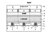
【解決手段】p型シリコン基板1上方に配列された多数の画素部を有する固体撮像素子であって、該画素部が、p型シリコン基板1上方に設けられた光電変換部(下部電極6、光電変換層7、上部電極8)と、該光電変換部上方に設けられたカラーフィルタ10とを含み、隣接する画素部のカラーフィルタ10同士の間に、画素部のカラーフィルタ10に入射した光が隣の画素部に入射するのを防止するための隔壁11を備える。
【選択図】図1
Description
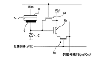
図2に示すように、信号読み出し回路4は、電荷蓄積部2に蓄積された信号電荷をリセットするためのリセットトランジスタ4aと、電荷蓄積部2に蓄積された信号電荷を電圧信号に変換するための出力トランジスタ4bと、出力トランジスタ4bから出力された電圧信号を列信号線に出力するための選択トランジスタ4cとを備えた公知の3トランジスタ構成となっている。p型シリコン基板1上には、これらトランジスタのゲート酸化膜3が形成されている。ゲート酸化膜3は例えば酸化シリコンで構成されている。
6 下部電極
7 光電変換層
8 上部電極
10 カラーフィルタ
11 隔壁
Claims (10)
- 基板上方に配列された多数の画素部を有する固体撮像素子であって、
前記画素部が、前記基板上方に設けられた光電変換部と、前記光電変換部上方に設けられたカラーフィルタとを含み、
前記画素部の前記カラーフィルタに入射した光が隣の前記画素部に入射するのを防止するための隔壁を備える固体撮像素子。 - 請求項1記載の固体撮像素子であって、
前記隔壁が、隣接する前記画素部の前記カラーフィルタ同士の間に前記カラーフィルタの側面を覆って設けられている固体撮像素子。 - 請求項2記載の固体撮像素子であって、
前記隔壁が、光を吸収又は反射する材料で構成されたもの、又は、光を全反射する空気層である固体撮像素子。 - 請求項2又は3記載の固体撮像素子であって、
前記光電変換部が、前記光電変換部で発生した信号電荷に応じた信号を出力するための回路が形成される基板上に設けられた半導体基板内に形成されたフォトダイオードである固体撮像素子。 - 請求項2又は3記載の固体撮像素子であって、
前記光電変換部が、前記基板上方に設けられた下部電極、前記下部電極上方に設けられた上部電極、及び前記下部電極と前記上部電極の間に設けられた光電変換層を含み、
前記画素部が、前記カラーフィルタと前記上部電極との間に設けられた、前記光電変換部を保護するための保護層を含み、
前記隔壁が、隣接する前記画素部の前記保護層同士の間にも設けられている固体撮像素子。 - 請求項5記載の固体撮像素子であって、
前記隔壁が、隣接する前記画素部の前記光電変換部同士の間にも設けられている固体撮像素子。 - 請求項5又は6記載の固体撮像素子であって、
前記光電変換層が、可視域の光を吸収し、吸収した光に応じた信号電荷を発生する光電変換材料で構成されており、
前記多数の画素部に含まれる前記カラーフィルタが、それぞれ異なる波長域の光を透過する3種類以上のカラーフィルタを含む固体撮像素子。 - 請求項5〜7のいずれか1項記載の固体撮像素子であって、
前記光電変換層が有機又は無機の光電変換材料で構成されている固体撮像素子。 - 請求項1〜8のいずれか1項記載の固体撮像素子であって、
前記画素部が、前記カラーフィルタ上に、前記光電変換部に光を集光するためのマイクロレンズを備える固体撮像素子。 - 請求項1〜9のいずれか1項記載の固体撮像素子を備える撮像装置。
Priority Applications (2)
| Application Number | Priority Date | Filing Date | Title |
|---|---|---|---|
| JP2008233316A JP2010067827A (ja) | 2008-09-11 | 2008-09-11 | 固体撮像素子及び撮像装置 |
| US12/557,964 US8237834B2 (en) | 2008-09-11 | 2009-09-11 | Solid-state imaging device and imaging apparatus having light-preventing partitions |
Applications Claiming Priority (1)
| Application Number | Priority Date | Filing Date | Title |
|---|---|---|---|
| JP2008233316A JP2010067827A (ja) | 2008-09-11 | 2008-09-11 | 固体撮像素子及び撮像装置 |
Publications (2)
| Publication Number | Publication Date |
|---|---|
| JP2010067827A true JP2010067827A (ja) | 2010-03-25 |
| JP2010067827A5 JP2010067827A5 (ja) | 2011-04-21 |
Family
ID=41798938
Family Applications (1)
| Application Number | Title | Priority Date | Filing Date |
|---|---|---|---|
| JP2008233316A Abandoned JP2010067827A (ja) | 2008-09-11 | 2008-09-11 | 固体撮像素子及び撮像装置 |
Country Status (2)
| Country | Link |
|---|---|
| US (1) | US8237834B2 (ja) |
| JP (1) | JP2010067827A (ja) |
Cited By (27)
| Publication number | Priority date | Publication date | Assignee | Title |
|---|---|---|---|---|
| US20100253819A1 (en) * | 2008-07-25 | 2010-10-07 | Panasonic Corporation | Solid state imaging device and method for manufacturing the same |
| WO2011141974A1 (ja) * | 2010-05-11 | 2011-11-17 | パナソニック株式会社 | 固体撮像素子及びその製造方法 |
| WO2011148437A1 (ja) * | 2010-05-28 | 2011-12-01 | パナソニック株式会社 | 固体撮像素子 |
| WO2012066694A1 (ja) * | 2010-11-17 | 2012-05-24 | パナソニック株式会社 | 固体撮像装置とその製造方法 |
| WO2012157730A1 (en) * | 2011-05-13 | 2012-11-22 | Fujifilm Corporation | Imaging apparatus |
| JP2013229528A (ja) * | 2012-04-27 | 2013-11-07 | Fujifilm Corp | 固体撮像素子 |
| WO2013164948A1 (ja) * | 2012-05-01 | 2013-11-07 | ソニー株式会社 | 固体撮像装置及びその製造方法、電子機器 |
| JP2014022448A (ja) * | 2012-07-13 | 2014-02-03 | Toshiba Corp | 固体撮像装置 |
| WO2014021115A1 (ja) * | 2012-07-30 | 2014-02-06 | ソニー株式会社 | 固体撮像装置、固体撮像装置の製造方法及び電子機器 |
| JP2014067948A (ja) * | 2012-09-27 | 2014-04-17 | Fujifilm Corp | 固体撮像素子および撮像装置 |
| JP2014138071A (ja) * | 2013-01-16 | 2014-07-28 | Canon Inc | 固体撮像装置及びその製造方法 |
| JP2014138067A (ja) * | 2013-01-16 | 2014-07-28 | Canon Inc | 固体撮像装置の製造方法 |
| KR101449829B1 (ko) * | 2012-07-31 | 2014-10-08 | 타이완 세미콘덕터 매뉴팩쳐링 컴퍼니 리미티드 | 적층된 방식의 융기된 광다이오드 |
| JP2014225667A (ja) * | 2013-05-16 | 2014-12-04 | 采▲ぎょく▼科技股▲ふん▼有限公司VisEra Technologies Company Limited | Bsi型cmosイメージセンサ |
| KR20150031175A (ko) * | 2013-09-13 | 2015-03-23 | 타이완 세미콘덕터 매뉴팩쳐링 컴퍼니 리미티드 | 포토 다이오드 및 이의 형성 방법 |
| JP2015073070A (ja) * | 2013-10-02 | 2015-04-16 | 采▲ぎょく▼科技股▲ふん▼有限公司VisEra Technologies Company Limited | 光電変換層の隔壁を有する撮像装置 |
| JP2016032053A (ja) * | 2014-07-30 | 2016-03-07 | キヤノン株式会社 | 撮像装置、および、撮像システム |
| US9343492B2 (en) | 2013-12-30 | 2016-05-17 | Samsung Electronics Co., Ltd. | CMOS image sensor based on thin-film on asic and operating method thereof |
| US9386206B2 (en) | 2012-03-30 | 2016-07-05 | Fujifilm Corporation | Imaging element and imaging device |
| WO2016185914A1 (ja) * | 2015-05-19 | 2016-11-24 | ソニーセミコンダクタソリューションズ株式会社 | 半導体装置、固体撮像装置、電子機器、および半導体装置の製造方法 |
| US9876046B2 (en) | 2015-04-02 | 2018-01-23 | Panasonic Intellectual Property Management Co., Ltd. | Imaging device comprising multilayer wiring structure and capacitance element capable of having relatively larger capacitance value |
| WO2018016181A1 (ja) * | 2016-07-20 | 2018-01-25 | ソニー株式会社 | 受光素子、受光素子の製造方法、撮像装置および電子機器 |
| WO2018155183A1 (ja) * | 2017-02-21 | 2018-08-30 | ソニーセミコンダクタソリューションズ株式会社 | 撮像素子および電子機器 |
| JP2019135789A (ja) * | 2019-04-22 | 2019-08-15 | キヤノン株式会社 | 固体撮像素子および撮像システム |
| KR20200097330A (ko) * | 2017-12-21 | 2020-08-18 | 이쏘그 | 화상 센서 |
| WO2023013307A1 (ja) * | 2021-08-06 | 2023-02-09 | ソニーセミコンダクタソリューションズ株式会社 | 固体撮像素子および電子機器 |
| JP7450651B2 (ja) | 2021-08-02 | 2024-03-15 | 采▲ぎょく▼科技股▲ふん▼有限公司 | イメージセンサおよびその形成方法 |
Families Citing this family (29)
| Publication number | Priority date | Publication date | Assignee | Title |
|---|---|---|---|---|
| JP5671789B2 (ja) * | 2009-08-10 | 2015-02-18 | ソニー株式会社 | 固体撮像装置とその製造方法および撮像装置 |
| US8736733B2 (en) * | 2010-03-19 | 2014-05-27 | Invisage Technologies, Inc. | Dark current reduction in image sensors via dynamic electrical biasing |
| JP5468133B2 (ja) * | 2010-05-14 | 2014-04-09 | パナソニック株式会社 | 固体撮像装置 |
| FR2965976A1 (fr) * | 2010-10-08 | 2012-04-13 | St Microelectronics Sa | Capteur d'images eclaire par la face arriere |
| US8878969B2 (en) * | 2011-07-27 | 2014-11-04 | Aptina Imaging Corporation | Imaging systems with color filter barriers |
| US9224770B2 (en) | 2012-04-26 | 2015-12-29 | Taiwan Semiconductor Manufacturing Company, Ltd. | Image sensor device and method |
| US9455288B2 (en) * | 2012-05-21 | 2016-09-27 | Taiwan Semiconductor Manufacturing Company, Ltd. | Image sensor structure to reduce cross-talk and improve quantum efficiency |
| KR101989907B1 (ko) | 2012-05-31 | 2019-06-17 | 삼성전자주식회사 | 유기 이미지 센서 및 그 제조방법 |
| US8933527B2 (en) | 2012-07-31 | 2015-01-13 | Taiwan Semiconductor Manufacturing Company, Ltd. | Elevated photodiodes with crosstalk isolation |
| US9502453B2 (en) * | 2013-03-14 | 2016-11-22 | Visera Technologies Company Limited | Solid-state imaging devices |
| CN103296042A (zh) * | 2013-05-30 | 2013-09-11 | 豪威科技(上海)有限公司 | 背照式cmos影像传感器及其制造方法 |
| JP6060851B2 (ja) * | 2013-08-09 | 2017-01-18 | ソニー株式会社 | 固体撮像装置の製造方法 |
| JP6541313B2 (ja) * | 2014-07-31 | 2019-07-10 | キヤノン株式会社 | 光電変換装置、及び撮像システム |
| US10104322B2 (en) | 2014-07-31 | 2018-10-16 | Invisage Technologies, Inc. | Image sensors with noise reduction |
| JP6682175B2 (ja) * | 2014-07-31 | 2020-04-15 | キヤノン株式会社 | 固体撮像素子および撮像システム |
| JP6521586B2 (ja) * | 2014-07-31 | 2019-05-29 | キヤノン株式会社 | 固体撮像素子および撮像システム |
| TWI700824B (zh) * | 2015-02-09 | 2020-08-01 | 日商索尼半導體解決方案公司 | 攝像元件及電子裝置 |
| US9497366B1 (en) | 2015-05-27 | 2016-11-15 | Semiconductor Components Industries, Llc | Imaging systems with integrated light shield structures |
| CN107039468B (zh) | 2015-08-06 | 2020-10-23 | 联华电子股份有限公司 | 影像感测器及其制作方法 |
| US10038019B2 (en) | 2015-12-29 | 2018-07-31 | Industrial Technology Research Institute | Image sensor and manufacturing method thereof |
| US10038033B2 (en) * | 2015-12-29 | 2018-07-31 | Industrial Technology Research Institute | Image sensor |
| TWI646677B (zh) * | 2015-12-29 | 2019-01-01 | 財團法人工業技術研究院 | 影像感測器及其製造方法 |
| JP7000020B2 (ja) * | 2016-11-30 | 2022-01-19 | キヤノン株式会社 | 光電変換装置、撮像システム |
| US10164156B2 (en) * | 2017-03-31 | 2018-12-25 | Taiwan Semiconductor Manufacturing Co., Ltd. | Structure and formation method of image sensor structure with grid structure |
| US10425601B1 (en) | 2017-05-05 | 2019-09-24 | Invisage Technologies, Inc. | Three-transistor active reset pixel |
| JP6987529B2 (ja) * | 2017-05-15 | 2022-01-05 | ソニーセミコンダクタソリューションズ株式会社 | 撮像素子、撮像素子の製造方法、電子機器、及び、撮像モジュール |
| TWI649865B (zh) * | 2017-09-06 | 2019-02-01 | 財團法人工業技術研究院 | 影像感測器及其製造方法 |
| KR102506837B1 (ko) * | 2017-11-20 | 2023-03-06 | 삼성전자주식회사 | 이미지 센서 및 그 제조 방법 |
| KR20200029098A (ko) | 2018-09-07 | 2020-03-18 | 삼성전자주식회사 | 이미지 센서 및 그 제조 방법 |
Citations (16)
| Publication number | Priority date | Publication date | Assignee | Title |
|---|---|---|---|---|
| JPH0451568A (ja) * | 1990-06-20 | 1992-02-20 | Hitachi Ltd | カラー固体撮像素子及びその製造方法 |
| JPH0420249U (ja) * | 1990-06-13 | 1992-02-20 | ||
| JPH05291549A (ja) * | 1992-04-06 | 1993-11-05 | Ricoh Co Ltd | 積層型固体撮像デバイス |
| JPH09172154A (ja) * | 1995-11-20 | 1997-06-30 | Eastman Kodak Co | 埋め込まれたカラーフィルタ要素を有するccd用の平坦なカラーフィルタ配列 |
| JP2002057318A (ja) * | 2000-08-07 | 2002-02-22 | Sony Corp | 固体撮像素子及びその製造方法 |
| JP2002151670A (ja) * | 2000-08-30 | 2002-05-24 | Sony Corp | 固体撮像装置および製造方法 |
| JP2002231929A (ja) * | 2001-02-06 | 2002-08-16 | Sony Corp | 固体撮像素子 |
| JP2003332544A (ja) * | 2002-05-14 | 2003-11-21 | Sanyo Electric Co Ltd | 固体撮像素子及びその製造方法 |
| JP2006093292A (ja) * | 2004-09-22 | 2006-04-06 | Matsushita Electric Ind Co Ltd | 固体撮像装置 |
| JP2006196553A (ja) * | 2005-01-11 | 2006-07-27 | Matsushita Electric Ind Co Ltd | 固体撮像装置 |
| JP2006295125A (ja) * | 2005-01-18 | 2006-10-26 | Matsushita Electric Ind Co Ltd | 固体撮像装置及びその製造方法並びにカメラ |
| WO2006129762A1 (ja) * | 2005-06-02 | 2006-12-07 | Sony Corporation | 半導体イメージセンサ・モジュール及びその製造方法 |
| JP2007005493A (ja) * | 2005-06-22 | 2007-01-11 | Sharp Corp | 固体撮像素子およびその製造方法、電子情報機器 |
| WO2008034838A2 (fr) * | 2006-09-19 | 2008-03-27 | E2V Semiconductors | Capteur d'image en couleur a diaphotie améliorée |
| JP2008085159A (ja) * | 2006-09-28 | 2008-04-10 | Fujifilm Corp | 撮像素子及び内視鏡装置 |
| JP2008182185A (ja) * | 2007-01-24 | 2008-08-07 | Taiwan Semiconductor Manufacturing Co Ltd | 裏面照射型半導体装置およびその製造方法 |
Family Cites Families (4)
| Publication number | Priority date | Publication date | Assignee | Title |
|---|---|---|---|---|
| US20050195318A1 (en) * | 2003-02-07 | 2005-09-08 | Takahiro Komatsu | Organic information reading unit and information reading device using the same |
| JP2005347475A (ja) | 2004-06-02 | 2005-12-15 | Fuji Photo Film Co Ltd | 固体撮像素子、及び固体撮像システム |
| KR100710210B1 (ko) * | 2005-09-28 | 2007-04-20 | 동부일렉트로닉스 주식회사 | 씨모스 이미지 센서 및 그 제조방법 |
| US8111286B2 (en) * | 2006-09-28 | 2012-02-07 | Fujifilm Corporation | Image processing apparatus, endoscope, and computer readable medium |
-
2008
- 2008-09-11 JP JP2008233316A patent/JP2010067827A/ja not_active Abandoned
-
2009
- 2009-09-11 US US12/557,964 patent/US8237834B2/en active Active
Patent Citations (16)
| Publication number | Priority date | Publication date | Assignee | Title |
|---|---|---|---|---|
| JPH0420249U (ja) * | 1990-06-13 | 1992-02-20 | ||
| JPH0451568A (ja) * | 1990-06-20 | 1992-02-20 | Hitachi Ltd | カラー固体撮像素子及びその製造方法 |
| JPH05291549A (ja) * | 1992-04-06 | 1993-11-05 | Ricoh Co Ltd | 積層型固体撮像デバイス |
| JPH09172154A (ja) * | 1995-11-20 | 1997-06-30 | Eastman Kodak Co | 埋め込まれたカラーフィルタ要素を有するccd用の平坦なカラーフィルタ配列 |
| JP2002057318A (ja) * | 2000-08-07 | 2002-02-22 | Sony Corp | 固体撮像素子及びその製造方法 |
| JP2002151670A (ja) * | 2000-08-30 | 2002-05-24 | Sony Corp | 固体撮像装置および製造方法 |
| JP2002231929A (ja) * | 2001-02-06 | 2002-08-16 | Sony Corp | 固体撮像素子 |
| JP2003332544A (ja) * | 2002-05-14 | 2003-11-21 | Sanyo Electric Co Ltd | 固体撮像素子及びその製造方法 |
| JP2006093292A (ja) * | 2004-09-22 | 2006-04-06 | Matsushita Electric Ind Co Ltd | 固体撮像装置 |
| JP2006196553A (ja) * | 2005-01-11 | 2006-07-27 | Matsushita Electric Ind Co Ltd | 固体撮像装置 |
| JP2006295125A (ja) * | 2005-01-18 | 2006-10-26 | Matsushita Electric Ind Co Ltd | 固体撮像装置及びその製造方法並びにカメラ |
| WO2006129762A1 (ja) * | 2005-06-02 | 2006-12-07 | Sony Corporation | 半導体イメージセンサ・モジュール及びその製造方法 |
| JP2007005493A (ja) * | 2005-06-22 | 2007-01-11 | Sharp Corp | 固体撮像素子およびその製造方法、電子情報機器 |
| WO2008034838A2 (fr) * | 2006-09-19 | 2008-03-27 | E2V Semiconductors | Capteur d'image en couleur a diaphotie améliorée |
| JP2008085159A (ja) * | 2006-09-28 | 2008-04-10 | Fujifilm Corp | 撮像素子及び内視鏡装置 |
| JP2008182185A (ja) * | 2007-01-24 | 2008-08-07 | Taiwan Semiconductor Manufacturing Co Ltd | 裏面照射型半導体装置およびその製造方法 |
Cited By (54)
| Publication number | Priority date | Publication date | Assignee | Title |
|---|---|---|---|---|
| US20100253819A1 (en) * | 2008-07-25 | 2010-10-07 | Panasonic Corporation | Solid state imaging device and method for manufacturing the same |
| WO2011141974A1 (ja) * | 2010-05-11 | 2011-11-17 | パナソニック株式会社 | 固体撮像素子及びその製造方法 |
| WO2011148437A1 (ja) * | 2010-05-28 | 2011-12-01 | パナソニック株式会社 | 固体撮像素子 |
| WO2012066694A1 (ja) * | 2010-11-17 | 2012-05-24 | パナソニック株式会社 | 固体撮像装置とその製造方法 |
| WO2012157730A1 (en) * | 2011-05-13 | 2012-11-22 | Fujifilm Corporation | Imaging apparatus |
| JP2012238774A (ja) * | 2011-05-13 | 2012-12-06 | Fujifilm Corp | 撮像装置 |
| US8988565B2 (en) | 2011-05-13 | 2015-03-24 | Fujifilm Corporation | Imaging apparatus |
| US9386206B2 (en) | 2012-03-30 | 2016-07-05 | Fujifilm Corporation | Imaging element and imaging device |
| JP2013229528A (ja) * | 2012-04-27 | 2013-11-07 | Fujifilm Corp | 固体撮像素子 |
| WO2013164948A1 (ja) * | 2012-05-01 | 2013-11-07 | ソニー株式会社 | 固体撮像装置及びその製造方法、電子機器 |
| US9293722B2 (en) | 2012-05-01 | 2016-03-22 | Sony Corporation | Solid-state image pickup device, method of manufacturing the same, and electronic apparatus |
| JP2014022448A (ja) * | 2012-07-13 | 2014-02-03 | Toshiba Corp | 固体撮像装置 |
| US11032497B2 (en) * | 2012-07-30 | 2021-06-08 | Sony Corporation | Solid state imaging device, method of manufacturing solid-state imaging device, and electronic apparatus |
| US11546533B2 (en) | 2012-07-30 | 2023-01-03 | Sony Group Corporation | Solid state imaging device, method of manufacturing solid-state imaging device, and electronic apparatus |
| US9496303B2 (en) | 2012-07-30 | 2016-11-15 | Sony Corporation | Solid state imaging device, method of manufacturing solid-state imaging device, and electronic apparatus |
| US11849081B2 (en) | 2012-07-30 | 2023-12-19 | Sony Group Corporation | Solid state imaging device, method of manufacturing solid-state imaging device, and electronic apparatus |
| WO2014021115A1 (ja) * | 2012-07-30 | 2014-02-06 | ソニー株式会社 | 固体撮像装置、固体撮像装置の製造方法及び電子機器 |
| US9530811B2 (en) | 2012-07-31 | 2016-12-27 | Taiwan Semiconductor Manufacturing Company, Ltd. | Elevated photodiode with a stacked scheme |
| KR101449829B1 (ko) * | 2012-07-31 | 2014-10-08 | 타이완 세미콘덕터 매뉴팩쳐링 컴퍼니 리미티드 | 적층된 방식의 융기된 광다이오드 |
| US9123617B2 (en) | 2012-07-31 | 2015-09-01 | Taiwan Semiconductor Manufacturing Company, Ltd. | Elevated photodiode with a stacked scheme |
| US10510791B2 (en) | 2012-07-31 | 2019-12-17 | Taiwan Semiconductor Manufacturing Company, Ltd. | Elevated photodiode with a stacked scheme |
| US10062721B2 (en) | 2012-07-31 | 2018-08-28 | Taiwan Semiconductor Manufacturing Company, Ltd. | Elevated photodiode with a stacked scheme |
| US8878325B2 (en) | 2012-07-31 | 2014-11-04 | Taiwan Semiconductor Manufacturing Company, Ltd. | Elevated photodiode with a stacked scheme |
| JP2014067948A (ja) * | 2012-09-27 | 2014-04-17 | Fujifilm Corp | 固体撮像素子および撮像装置 |
| JP2014138067A (ja) * | 2013-01-16 | 2014-07-28 | Canon Inc | 固体撮像装置の製造方法 |
| JP2014138071A (ja) * | 2013-01-16 | 2014-07-28 | Canon Inc | 固体撮像装置及びその製造方法 |
| JP2014225667A (ja) * | 2013-05-16 | 2014-12-04 | 采▲ぎょく▼科技股▲ふん▼有限公司VisEra Technologies Company Limited | Bsi型cmosイメージセンサ |
| KR20150031175A (ko) * | 2013-09-13 | 2015-03-23 | 타이완 세미콘덕터 매뉴팩쳐링 컴퍼니 리미티드 | 포토 다이오드 및 이의 형성 방법 |
| KR101672590B1 (ko) | 2013-09-13 | 2016-11-03 | 타이완 세미콘덕터 매뉴팩쳐링 컴퍼니 리미티드 | 포토 다이오드 및 이의 형성 방법 |
| JP2015073070A (ja) * | 2013-10-02 | 2015-04-16 | 采▲ぎょく▼科技股▲ふん▼有限公司VisEra Technologies Company Limited | 光電変換層の隔壁を有する撮像装置 |
| US9343492B2 (en) | 2013-12-30 | 2016-05-17 | Samsung Electronics Co., Ltd. | CMOS image sensor based on thin-film on asic and operating method thereof |
| JP2016032053A (ja) * | 2014-07-30 | 2016-03-07 | キヤノン株式会社 | 撮像装置、および、撮像システム |
| US10490591B2 (en) | 2015-04-02 | 2019-11-26 | Panasonic Intellectual Property Management Co., Ltd. | Imaging device comprising multilayer wiring structure and capacitance element capable of having relatively large capacitance value |
| US9876046B2 (en) | 2015-04-02 | 2018-01-23 | Panasonic Intellectual Property Management Co., Ltd. | Imaging device comprising multilayer wiring structure and capacitance element capable of having relatively larger capacitance value |
| WO2016185914A1 (ja) * | 2015-05-19 | 2016-11-24 | ソニーセミコンダクタソリューションズ株式会社 | 半導体装置、固体撮像装置、電子機器、および半導体装置の製造方法 |
| US10622563B2 (en) | 2015-05-19 | 2020-04-14 | Sony Semiconductor Solutions Corporation | Semiconductor device, solid-state imaging device, electronic apparatus, and manufacturing method of semiconductor device |
| WO2018016181A1 (ja) * | 2016-07-20 | 2018-01-25 | ソニー株式会社 | 受光素子、受光素子の製造方法、撮像装置および電子機器 |
| JPWO2018016181A1 (ja) * | 2016-07-20 | 2019-05-09 | ソニー株式会社 | 受光素子、受光素子の製造方法、撮像装置および電子機器 |
| CN109314124A (zh) * | 2016-07-20 | 2019-02-05 | 索尼公司 | 受光元件及其制造方法、成像器件和电子装置 |
| CN109314124B (zh) * | 2016-07-20 | 2023-05-12 | 索尼公司 | 受光元件及其制造方法、成像器件和电子装置 |
| KR20190028376A (ko) * | 2016-07-20 | 2019-03-18 | 소니 주식회사 | 수광 소자, 수광 소자의 제조 방법, 촬상 장치 및 전자 기기 |
| US10818718B2 (en) | 2016-07-20 | 2020-10-27 | Sony Corporation | Light receiving element, method of manufacturing light receiving element, imaging device, and electronic apparatus |
| KR102413726B1 (ko) * | 2016-07-20 | 2022-06-28 | 소니그룹주식회사 | 수광 소자, 수광 소자의 제조 방법, 촬상 장치 및 전자 기기 |
| WO2018155183A1 (ja) * | 2017-02-21 | 2018-08-30 | ソニーセミコンダクタソリューションズ株式会社 | 撮像素子および電子機器 |
| US11069739B2 (en) | 2017-02-21 | 2021-07-20 | Sony Semiconductor Solutions Corporation | Imaging device and electronic apparatus |
| JPWO2018155183A1 (ja) * | 2017-02-21 | 2019-12-12 | ソニーセミコンダクタソリューションズ株式会社 | 撮像素子および電子機器 |
| JP2021507529A (ja) * | 2017-12-21 | 2021-02-22 | イソルグ | 画像センサ |
| KR20200097330A (ko) * | 2017-12-21 | 2020-08-18 | 이쏘그 | 화상 센서 |
| JP7333323B2 (ja) | 2017-12-21 | 2023-08-24 | イソルグ | 画像センサ |
| KR102592059B1 (ko) * | 2017-12-21 | 2023-10-19 | 이쏘그 | 화상 센서 |
| JP7134911B2 (ja) | 2019-04-22 | 2022-09-12 | キヤノン株式会社 | 固体撮像素子および撮像システム |
| JP2019135789A (ja) * | 2019-04-22 | 2019-08-15 | キヤノン株式会社 | 固体撮像素子および撮像システム |
| JP7450651B2 (ja) | 2021-08-02 | 2024-03-15 | 采▲ぎょく▼科技股▲ふん▼有限公司 | イメージセンサおよびその形成方法 |
| WO2023013307A1 (ja) * | 2021-08-06 | 2023-02-09 | ソニーセミコンダクタソリューションズ株式会社 | 固体撮像素子および電子機器 |
Also Published As
| Publication number | Publication date |
|---|---|
| US8237834B2 (en) | 2012-08-07 |
| US20100060769A1 (en) | 2010-03-11 |
Similar Documents
| Publication | Publication Date | Title |
|---|---|---|
| JP2010067827A (ja) | 固体撮像素子及び撮像装置 | |
| JP7301936B2 (ja) | 固体撮像素子およびその製造方法、並びに電子機器 | |
| JP5478043B2 (ja) | 固体撮像素子及び撮像装置 | |
| US11282881B2 (en) | Solid-state imaging device and method of manufacturing the same, and imaging apparatus | |
| US10074682B2 (en) | Phase difference detection in pixels | |
| JP4826111B2 (ja) | 固体撮像素子および固体撮像素子の製造方法および画像撮影装置 | |
| KR102129147B1 (ko) | 고체 촬상 소자, 고체 촬상 소자의 제조 방법, 및, 전자기기 | |
| US9349766B2 (en) | Solid-state imaging device | |
| JP5708025B2 (ja) | 固体撮像装置、および、その製造方法、電子機器 | |
| JP2016127264A (ja) | 固体撮像素子およびその製造方法、並びに電子機器 | |
| JP2015065270A (ja) | 固体撮像装置およびその製造方法、並びに電子機器 | |
| WO2016104177A1 (ja) | 固体撮像素子およびその製造方法、並びに電子機器 | |
| JP5287923B2 (ja) | 固体撮像素子および固体撮像素子の製造方法及び画像撮影装置 | |
| JP5371339B2 (ja) | 固体撮像素子及び撮像装置 | |
| WO2021215303A1 (ja) | 固体撮像素子および電子機器 | |
| JP2020027937A (ja) | 固体撮像装置、固体撮像装置の製造方法、および電子機器 | |
| JP5282797B2 (ja) | 固体撮像素子および固体撮像素子の製造方法及び画像撮影装置 | |
| JP5263220B2 (ja) | 固体撮像装置、その製造方法および撮像装置 | |
| JP5825398B2 (ja) | 固体撮像素子及び固体撮像素子の製造方法、電子機器 | |
| JP2008047608A (ja) | 単板式カラー固体撮像素子 | |
| KR20220149516A (ko) | 고체 촬상 장치 및 전자 기기 | |
| JP2007208139A (ja) | 固体撮像素子の製造方法、固体撮像素子 | |
| KR20070081702A (ko) | 이미지 센서 및 그 형성 방법 |
Legal Events
| Date | Code | Title | Description |
|---|---|---|---|
| A521 | Request for written amendment filed |
Free format text: JAPANESE INTERMEDIATE CODE: A523 Effective date: 20110307 |
|
| A621 | Written request for application examination |
Free format text: JAPANESE INTERMEDIATE CODE: A621 Effective date: 20110307 |
|
| RD04 | Notification of resignation of power of attorney |
Free format text: JAPANESE INTERMEDIATE CODE: A7424 Effective date: 20111216 |
|
| RD03 | Notification of appointment of power of attorney |
Free format text: JAPANESE INTERMEDIATE CODE: A7423 Effective date: 20120914 |
|
| RD04 | Notification of resignation of power of attorney |
Free format text: JAPANESE INTERMEDIATE CODE: A7424 Effective date: 20121004 |
|
| A131 | Notification of reasons for refusal |
Free format text: JAPANESE INTERMEDIATE CODE: A131 Effective date: 20121016 |
|
| A762 | Written abandonment of application |
Free format text: JAPANESE INTERMEDIATE CODE: A762 Effective date: 20121126 |