JP2010034349A - 半導体装置の製造方法およびリードフレーム - Google Patents
半導体装置の製造方法およびリードフレーム Download PDFInfo
- Publication number
- JP2010034349A JP2010034349A JP2008195785A JP2008195785A JP2010034349A JP 2010034349 A JP2010034349 A JP 2010034349A JP 2008195785 A JP2008195785 A JP 2008195785A JP 2008195785 A JP2008195785 A JP 2008195785A JP 2010034349 A JP2010034349 A JP 2010034349A
- Authority
- JP
- Japan
- Prior art keywords
- island
- sealing resin
- semiconductor device
- lead
- main surface
- Prior art date
- Legal status (The legal status is an assumption and is not a legal conclusion. Google has not performed a legal analysis and makes no representation as to the accuracy of the status listed.)
- Granted
Links
- 239000004065 semiconductor Substances 0.000 title claims abstract description 100
- 238000004519 manufacturing process Methods 0.000 title claims abstract description 27
- 238000007789 sealing Methods 0.000 claims abstract description 99
- 229920005989 resin Polymers 0.000 claims abstract description 98
- 239000011347 resin Substances 0.000 claims abstract description 98
- 239000007788 liquid Substances 0.000 claims description 8
- 238000001746 injection moulding Methods 0.000 claims description 5
- 239000007787 solid Substances 0.000 claims description 5
- 238000002347 injection Methods 0.000 abstract description 2
- 239000007924 injection Substances 0.000 abstract description 2
- 238000000465 moulding Methods 0.000 abstract description 2
- 239000011800 void material Substances 0.000 abstract description 2
- 239000000243 solution Substances 0.000 abstract 1
- 238000003825 pressing Methods 0.000 description 19
- 238000000034 method Methods 0.000 description 16
- 229910052751 metal Inorganic materials 0.000 description 13
- 239000002184 metal Substances 0.000 description 13
- RYGMFSIKBFXOCR-UHFFFAOYSA-N Copper Chemical compound [Cu] RYGMFSIKBFXOCR-UHFFFAOYSA-N 0.000 description 5
- 229910052802 copper Inorganic materials 0.000 description 5
- 239000010949 copper Substances 0.000 description 5
- 230000017525 heat dissipation Effects 0.000 description 5
- 239000000463 material Substances 0.000 description 5
- 229910001111 Fine metal Inorganic materials 0.000 description 4
- 238000005530 etching Methods 0.000 description 3
- 239000000945 filler Substances 0.000 description 3
- VYPSYNLAJGMNEJ-UHFFFAOYSA-N Silicium dioxide Chemical compound O=[Si]=O VYPSYNLAJGMNEJ-UHFFFAOYSA-N 0.000 description 2
- 229910052782 aluminium Inorganic materials 0.000 description 2
- XAGFODPZIPBFFR-UHFFFAOYSA-N aluminium Chemical compound [Al] XAGFODPZIPBFFR-UHFFFAOYSA-N 0.000 description 2
- 238000004080 punching Methods 0.000 description 2
- 229920005992 thermoplastic resin Polymers 0.000 description 2
- 229920001187 thermosetting polymer Polymers 0.000 description 2
- 239000004925 Acrylic resin Substances 0.000 description 1
- 229920000178 Acrylic resin Polymers 0.000 description 1
- PNEYBMLMFCGWSK-UHFFFAOYSA-N aluminium oxide Inorganic materials [O-2].[O-2].[O-2].[Al+3].[Al+3] PNEYBMLMFCGWSK-UHFFFAOYSA-N 0.000 description 1
- 238000013459 approach Methods 0.000 description 1
- 238000006073 displacement reaction Methods 0.000 description 1
- 239000003822 epoxy resin Substances 0.000 description 1
- 230000005496 eutectics Effects 0.000 description 1
- 230000005669 field effect Effects 0.000 description 1
- 239000011888 foil Substances 0.000 description 1
- 238000010438 heat treatment Methods 0.000 description 1
- 238000009413 insulation Methods 0.000 description 1
- 230000001788 irregular Effects 0.000 description 1
- 239000011159 matrix material Substances 0.000 description 1
- 229910044991 metal oxide Inorganic materials 0.000 description 1
- 150000004706 metal oxides Chemical class 0.000 description 1
- 239000000203 mixture Substances 0.000 description 1
- 230000002093 peripheral effect Effects 0.000 description 1
- 238000007747 plating Methods 0.000 description 1
- 229920000647 polyepoxide Polymers 0.000 description 1
- 239000000377 silicon dioxide Substances 0.000 description 1
- 229910000679 solder Inorganic materials 0.000 description 1
- 239000000758 substrate Substances 0.000 description 1
- 238000001721 transfer moulding Methods 0.000 description 1
- 238000001039 wet etching Methods 0.000 description 1
Images


Classifications
-
- H—ELECTRICITY
- H01—ELECTRIC ELEMENTS
- H01L—SEMICONDUCTOR DEVICES NOT COVERED BY CLASS H10
- H01L24/00—Arrangements for connecting or disconnecting semiconductor or solid-state bodies; Methods or apparatus related thereto
- H01L24/93—Batch processes
- H01L24/95—Batch processes at chip-level, i.e. with connecting carried out on a plurality of singulated devices, i.e. on diced chips
- H01L24/97—Batch processes at chip-level, i.e. with connecting carried out on a plurality of singulated devices, i.e. on diced chips the devices being connected to a common substrate, e.g. interposer, said common substrate being separable into individual assemblies after connecting
-
- H—ELECTRICITY
- H01—ELECTRIC ELEMENTS
- H01L—SEMICONDUCTOR DEVICES NOT COVERED BY CLASS H10
- H01L2224/00—Indexing scheme for arrangements for connecting or disconnecting semiconductor or solid-state bodies and methods related thereto as covered by H01L24/00
- H01L2224/01—Means for bonding being attached to, or being formed on, the surface to be connected, e.g. chip-to-package, die-attach, "first-level" interconnects; Manufacturing methods related thereto
- H01L2224/42—Wire connectors; Manufacturing methods related thereto
- H01L2224/47—Structure, shape, material or disposition of the wire connectors after the connecting process
- H01L2224/48—Structure, shape, material or disposition of the wire connectors after the connecting process of an individual wire connector
- H01L2224/4805—Shape
- H01L2224/4809—Loop shape
- H01L2224/48091—Arched
-
- H—ELECTRICITY
- H01—ELECTRIC ELEMENTS
- H01L—SEMICONDUCTOR DEVICES NOT COVERED BY CLASS H10
- H01L2224/00—Indexing scheme for arrangements for connecting or disconnecting semiconductor or solid-state bodies and methods related thereto as covered by H01L24/00
- H01L2224/01—Means for bonding being attached to, or being formed on, the surface to be connected, e.g. chip-to-package, die-attach, "first-level" interconnects; Manufacturing methods related thereto
- H01L2224/42—Wire connectors; Manufacturing methods related thereto
- H01L2224/47—Structure, shape, material or disposition of the wire connectors after the connecting process
- H01L2224/48—Structure, shape, material or disposition of the wire connectors after the connecting process of an individual wire connector
- H01L2224/481—Disposition
- H01L2224/48151—Connecting between a semiconductor or solid-state body and an item not being a semiconductor or solid-state body, e.g. chip-to-substrate, chip-to-passive
- H01L2224/48221—Connecting between a semiconductor or solid-state body and an item not being a semiconductor or solid-state body, e.g. chip-to-substrate, chip-to-passive the body and the item being stacked
- H01L2224/48245—Connecting between a semiconductor or solid-state body and an item not being a semiconductor or solid-state body, e.g. chip-to-substrate, chip-to-passive the body and the item being stacked the item being metallic
- H01L2224/48247—Connecting between a semiconductor or solid-state body and an item not being a semiconductor or solid-state body, e.g. chip-to-substrate, chip-to-passive the body and the item being stacked the item being metallic connecting the wire to a bond pad of the item
-
- H—ELECTRICITY
- H01—ELECTRIC ELEMENTS
- H01L—SEMICONDUCTOR DEVICES NOT COVERED BY CLASS H10
- H01L2224/00—Indexing scheme for arrangements for connecting or disconnecting semiconductor or solid-state bodies and methods related thereto as covered by H01L24/00
- H01L2224/01—Means for bonding being attached to, or being formed on, the surface to be connected, e.g. chip-to-package, die-attach, "first-level" interconnects; Manufacturing methods related thereto
- H01L2224/42—Wire connectors; Manufacturing methods related thereto
- H01L2224/47—Structure, shape, material or disposition of the wire connectors after the connecting process
- H01L2224/48—Structure, shape, material or disposition of the wire connectors after the connecting process of an individual wire connector
- H01L2224/484—Connecting portions
- H01L2224/4847—Connecting portions the connecting portion on the bonding area of the semiconductor or solid-state body being a wedge bond
- H01L2224/48472—Connecting portions the connecting portion on the bonding area of the semiconductor or solid-state body being a wedge bond the other connecting portion not on the bonding area also being a wedge bond, i.e. wedge-to-wedge
-
- H—ELECTRICITY
- H01—ELECTRIC ELEMENTS
- H01L—SEMICONDUCTOR DEVICES NOT COVERED BY CLASS H10
- H01L2924/00—Indexing scheme for arrangements or methods for connecting or disconnecting semiconductor or solid-state bodies as covered by H01L24/00
- H01L2924/013—Alloys
- H01L2924/0132—Binary Alloys
- H01L2924/01322—Eutectic Alloys, i.e. obtained by a liquid transforming into two solid phases
-
- H—ELECTRICITY
- H01—ELECTRIC ELEMENTS
- H01L—SEMICONDUCTOR DEVICES NOT COVERED BY CLASS H10
- H01L2924/00—Indexing scheme for arrangements or methods for connecting or disconnecting semiconductor or solid-state bodies as covered by H01L24/00
- H01L2924/10—Details of semiconductor or other solid state devices to be connected
- H01L2924/11—Device type
- H01L2924/13—Discrete devices, e.g. 3 terminal devices
- H01L2924/1304—Transistor
- H01L2924/1305—Bipolar Junction Transistor [BJT]
- H01L2924/13055—Insulated gate bipolar transistor [IGBT]
-
- H—ELECTRICITY
- H01—ELECTRIC ELEMENTS
- H01L—SEMICONDUCTOR DEVICES NOT COVERED BY CLASS H10
- H01L2924/00—Indexing scheme for arrangements or methods for connecting or disconnecting semiconductor or solid-state bodies as covered by H01L24/00
- H01L2924/10—Details of semiconductor or other solid state devices to be connected
- H01L2924/11—Device type
- H01L2924/13—Discrete devices, e.g. 3 terminal devices
- H01L2924/1304—Transistor
- H01L2924/1306—Field-effect transistor [FET]
- H01L2924/13091—Metal-Oxide-Semiconductor Field-Effect Transistor [MOSFET]
-
- H—ELECTRICITY
- H01—ELECTRIC ELEMENTS
- H01L—SEMICONDUCTOR DEVICES NOT COVERED BY CLASS H10
- H01L2924/00—Indexing scheme for arrangements or methods for connecting or disconnecting semiconductor or solid-state bodies as covered by H01L24/00
- H01L2924/15—Details of package parts other than the semiconductor or other solid state devices to be connected
- H01L2924/181—Encapsulation
- H01L2924/1815—Shape
Abstract
【解決手段】本発明の半導体装置の製造方法では、半導体装置が実装されるアイランド12の側面を傾斜面11としている。この様にすることで、モールド金型のキャビティ66に、ゲート80から封止樹脂を注入すると、注入された封止樹脂はアイランド12の側面に設けた傾斜面11に接触する。そして、傾斜面11に沿って封止樹脂は流動して、アイランド12の下面の空間に充填される。従って、アイランド12の下面を薄く被覆するために、アイランド12の下方の空間が狭く形成されても、この空間にボイド無く封止樹脂を充填させることができる。
【選択図】図5
Description
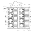
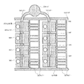
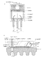
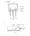
10A 半導体モジュール
11 傾斜面
12 アイランド
14,14A,14B,14C リード
16 封止樹脂
18 凹状部
20 半導体素子
22 貫通孔
24 平坦部
26 ヒートシンク
28 ビス
28A 頭部
28B 柱部
30 ワッシャ
32 孔部
34 金属細線
50 リードフレーム
52 外枠
56、56A、56B、56C、56D、56E、56F、56G、56H ユニット
58 タイバー
60 モールド金型
62 上金型
64 下金型
66、66A、66B、66C、66D、66E、66F、66G、66H キャビティ
68 押圧部
70 押圧部
72 ポッド
74 ランナー
76 ゲート
80 ゲート
82 エアベント
Claims (7)
- 第1主面と前記第1主面に対向する第2主面とを備えたアイランドと、前記アイランドに一端が接近するリードとを備え、前記第2側面と連続する部分の前記アイランドの側面が傾斜面であるリードフレームを用意する工程と、
前記アイランドの前記第1主面に半導体素子を実装し、前記半導体素子の電極と前記リードとを電気的に接続する工程と、
モールド金型を用いた射出成形により、前記アイランドの前記第2主面も含めて、前記アイランド、前記半導体素子および前記リードを封止樹脂により封止する工程と、を備え、
前記封止する工程では、
前記アイランドの側方に設けたゲートから、液状または半固形状の封止樹脂を前記モールド金型のキャビティに注入し、傾斜面である前記アイランドの側面に沿って前記封止樹脂を流動させることを特徴とする半導体装置の製造方法。 - 前記リードフレームには、前記アイランドと前記リードとから成るユニットが列状に配置され、個々のユニットに含まれる前記アイランドの一方向に面する側面に前記傾斜面が形成され、
前記封止する工程では、連通した複数のキャビティに前記ユニットを個別に収納した後に、前記金型に設けたポットから、前記列状に配置された前記キャビティに前記封止樹脂を順次供給することを特徴とする請求項1記載の半導体装置の製造方法。 - 前記アイランドの側面は、前記第2主面に近い方が前記ゲートから離間する傾斜面であることを特徴とする請求項2記載の半導体装置の製造方法。
- 前記アイランドの前記第2主面と前記モールド金型との間隙は、前記アイランドの前記第1主面と前記モールド金型との間隙よりも小さいことを特徴とする請求項3に記載の半導体装置の製造方法。
- 前記キャビティの内部に於ける前記アイランドの位置は固定されていることを特徴とする請求項4に記載の半導体装置の製造方法。
- 半導体素子が搭載される第1主面と、前記第1主面に対向する第2主面とを備えたアイランドと、
前記アイランドに一端が接近したリードと、を備え、
前記第2主面と連続する部分の前記アイランドの側面を傾斜面とすることを特徴とするリードフレーム。 - 前記アイランドと前記リードから成るユニットが列状に複数個設けられ、
個々のユニットの一方向に面する前記アイランドの前記側面を前記傾斜面とすることを特徴とする請求項6記載のリードフレーム。
Priority Applications (5)
| Application Number | Priority Date | Filing Date | Title |
|---|---|---|---|
| JP2008195785A JP5180722B2 (ja) | 2008-07-30 | 2008-07-30 | 半導体装置の製造方法 |
| CN201110429499.4A CN102522375B (zh) | 2008-07-30 | 2009-07-30 | 半导体装置、半导体装置的制造方法及引线框 |
| CN2009101636140A CN101640178B (zh) | 2008-07-30 | 2009-07-30 | 半导体装置、半导体装置的制造方法及引线框 |
| US12/512,802 US7839004B2 (en) | 2008-07-30 | 2009-07-30 | Semiconductor device, semiconductor module, method for manufacturing semiconductor device, and lead frame |
| US12/904,851 US8241958B2 (en) | 2008-07-30 | 2010-10-14 | Semiconductor device, semiconductor module, method for manufacturing semiconductor device, and lead frame |
Applications Claiming Priority (1)
| Application Number | Priority Date | Filing Date | Title |
|---|---|---|---|
| JP2008195785A JP5180722B2 (ja) | 2008-07-30 | 2008-07-30 | 半導体装置の製造方法 |
Publications (2)
| Publication Number | Publication Date |
|---|---|
| JP2010034349A true JP2010034349A (ja) | 2010-02-12 |
| JP5180722B2 JP5180722B2 (ja) | 2013-04-10 |
Family
ID=41615095
Family Applications (1)
| Application Number | Title | Priority Date | Filing Date |
|---|---|---|---|
| JP2008195785A Active JP5180722B2 (ja) | 2008-07-30 | 2008-07-30 | 半導体装置の製造方法 |
Country Status (2)
| Country | Link |
|---|---|
| JP (1) | JP5180722B2 (ja) |
| CN (1) | CN101640178B (ja) |
Cited By (1)
| Publication number | Priority date | Publication date | Assignee | Title |
|---|---|---|---|---|
| CN107799498A (zh) * | 2016-09-06 | 2018-03-13 | 精工半导体有限公司 | 半导体装置的制造方法 |
Families Citing this family (7)
| Publication number | Priority date | Publication date | Assignee | Title |
|---|---|---|---|---|
| DE102009002992B4 (de) * | 2009-05-11 | 2014-10-30 | Infineon Technologies Ag | Leistungshalbleitermodulanordnung mit eindeutig und verdrehsicher auf einem Kühlkörper montierbarem Leistungshalbleitermodul und Montageverfahren |
| JP5796956B2 (ja) * | 2010-12-24 | 2015-10-21 | セミコンダクター・コンポーネンツ・インダストリーズ・リミテッド・ライアビリティ・カンパニー | 回路装置およびその製造方法 |
| CN102376671A (zh) * | 2011-11-29 | 2012-03-14 | 杭州矽力杰半导体技术有限公司 | 引线框架以及应用其的倒装芯片式半导体封装结构 |
| JP2014082233A (ja) * | 2012-10-12 | 2014-05-08 | Sumitomo Electric Ind Ltd | 半導体装置及びその製造方法 |
| CN103094132B (zh) * | 2012-12-15 | 2017-12-26 | 华天科技(西安)有限公司 | 一种采用加宽模具假型腔优化二次塑封封装件的制作工艺 |
| KR20160038440A (ko) * | 2014-09-30 | 2016-04-07 | 삼성전기주식회사 | 전력 모듈 패키지와 이의 제작방법 |
| CN104332449A (zh) * | 2014-11-05 | 2015-02-04 | 无锡罗姆半导体科技有限公司 | 一种to-126型封装件 |
Citations (5)
| Publication number | Priority date | Publication date | Assignee | Title |
|---|---|---|---|---|
| JPH04186662A (ja) * | 1990-11-16 | 1992-07-03 | Hitachi Ltd | 半導体装置およびその製造方法 |
| JPH0521644A (ja) * | 1991-07-11 | 1993-01-29 | Sanken Electric Co Ltd | 樹脂封止型電子部品の製造方法 |
| JPH07335677A (ja) * | 1994-06-03 | 1995-12-22 | Rohm Co Ltd | パワー用半導体装置の製造方法 |
| JPH08204099A (ja) * | 1995-01-31 | 1996-08-09 | Rohm Co Ltd | 半導体装置の構造及び形成方法 |
| JP2004039800A (ja) * | 2002-07-02 | 2004-02-05 | Toshiba Components Co Ltd | リード端子型半導体装置 |
Family Cites Families (2)
| Publication number | Priority date | Publication date | Assignee | Title |
|---|---|---|---|---|
| JP2927660B2 (ja) * | 1993-01-25 | 1999-07-28 | シャープ株式会社 | 樹脂封止型半導体装置の製造方法 |
| US5817208A (en) * | 1995-08-04 | 1998-10-06 | Matsushita Electronics Corporation | Resin sealing die, resin-sealed-type semiconductor device and method of manufacturing the device |
-
2008
- 2008-07-30 JP JP2008195785A patent/JP5180722B2/ja active Active
-
2009
- 2009-07-30 CN CN2009101636140A patent/CN101640178B/zh not_active Expired - Fee Related
Patent Citations (5)
| Publication number | Priority date | Publication date | Assignee | Title |
|---|---|---|---|---|
| JPH04186662A (ja) * | 1990-11-16 | 1992-07-03 | Hitachi Ltd | 半導体装置およびその製造方法 |
| JPH0521644A (ja) * | 1991-07-11 | 1993-01-29 | Sanken Electric Co Ltd | 樹脂封止型電子部品の製造方法 |
| JPH07335677A (ja) * | 1994-06-03 | 1995-12-22 | Rohm Co Ltd | パワー用半導体装置の製造方法 |
| JPH08204099A (ja) * | 1995-01-31 | 1996-08-09 | Rohm Co Ltd | 半導体装置の構造及び形成方法 |
| JP2004039800A (ja) * | 2002-07-02 | 2004-02-05 | Toshiba Components Co Ltd | リード端子型半導体装置 |
Cited By (1)
| Publication number | Priority date | Publication date | Assignee | Title |
|---|---|---|---|---|
| CN107799498A (zh) * | 2016-09-06 | 2018-03-13 | 精工半导体有限公司 | 半导体装置的制造方法 |
Also Published As
| Publication number | Publication date |
|---|---|
| JP5180722B2 (ja) | 2013-04-10 |
| CN101640178B (zh) | 2012-08-15 |
| CN101640178A (zh) | 2010-02-03 |
Similar Documents
| Publication | Publication Date | Title |
|---|---|---|
| US7839004B2 (en) | Semiconductor device, semiconductor module, method for manufacturing semiconductor device, and lead frame | |
| JP5180722B2 (ja) | 半導体装置の製造方法 | |
| JP5339800B2 (ja) | 半導体装置の製造方法 | |
| US8203848B2 (en) | Circuit device and method of manufacturing the same | |
| EP2677539B1 (en) | Process for manufacture of a semiconductor device | |
| US7714455B2 (en) | Semiconductor packages and methods of fabricating the same | |
| US8105883B2 (en) | Molding die with tilted runner, method of manufacturing semiconductor device using the same, and semiconductor device made by the method | |
| JP6266168B2 (ja) | 半導体装置 | |
| KR20010107556A (ko) | 반도체 장치와 그 제조방법 | |
| JP2010034350A (ja) | 半導体装置 | |
| US8633511B2 (en) | Method of producing semiconductor device packaging having chips attached to islands separately and covered by encapsulation material | |
| JP5161688B2 (ja) | 半導体装置および半導体モジュール | |
| JP5341339B2 (ja) | 回路装置 | |
| KR20150060045A (ko) | 전력 모듈 패키지 및 그 제조 방법 | |
| JP5132407B2 (ja) | 半導体装置 | |
| JP2013004848A (ja) | 半導体装置およびその製造方法 | |
| JP2013187268A (ja) | 半導体モジュール | |
| JP2013020997A (ja) | 半導体装置の製造方法 | |
| JP2012178404A (ja) | 回路装置およびその製造方法 | |
| JP5341473B2 (ja) | 半導体装置およびその製造方法 | |
| JP2012019084A (ja) | 半導体装置及びその製造方法 | |
| JP2007012731A (ja) | 回路装置およびその製造方法 | |
| JP2008112928A (ja) | 回路装置の製造方法 | |
| JP2012151163A (ja) | 半導体モジュール |
Legal Events
| Date | Code | Title | Description |
|---|---|---|---|
| A711 | Notification of change in applicant |
Free format text: JAPANESE INTERMEDIATE CODE: A711 Effective date: 20110602 |
|
| A621 | Written request for application examination |
Free format text: JAPANESE INTERMEDIATE CODE: A621 Effective date: 20110620 |
|
| A977 | Report on retrieval |
Free format text: JAPANESE INTERMEDIATE CODE: A971007 Effective date: 20120829 |
|
| A131 | Notification of reasons for refusal |
Free format text: JAPANESE INTERMEDIATE CODE: A131 Effective date: 20120904 |
|
| A521 | Request for written amendment filed |
Free format text: JAPANESE INTERMEDIATE CODE: A523 Effective date: 20121130 |
|
| TRDD | Decision of grant or rejection written | ||
| A01 | Written decision to grant a patent or to grant a registration (utility model) |
Free format text: JAPANESE INTERMEDIATE CODE: A01 Effective date: 20121218 |
|
| A61 | First payment of annual fees (during grant procedure) |
Free format text: JAPANESE INTERMEDIATE CODE: A61 Effective date: 20130111 |
|
| R150 | Certificate of patent or registration of utility model |
Free format text: JAPANESE INTERMEDIATE CODE: R150 Ref document number: 5180722 Country of ref document: JP Free format text: JAPANESE INTERMEDIATE CODE: R150 |
|
| FPAY | Renewal fee payment (event date is renewal date of database) |
Free format text: PAYMENT UNTIL: 20160118 Year of fee payment: 3 |
|
| S111 | Request for change of ownership or part of ownership |
Free format text: JAPANESE INTERMEDIATE CODE: R313113 |
|
| FPAY | Renewal fee payment (event date is renewal date of database) |
Free format text: PAYMENT UNTIL: 20160118 Year of fee payment: 3 |
|
| R360 | Written notification for declining of transfer of rights |
Free format text: JAPANESE INTERMEDIATE CODE: R360 |
|
| R360 | Written notification for declining of transfer of rights |
Free format text: JAPANESE INTERMEDIATE CODE: R360 |
|
| R371 | Transfer withdrawn |
Free format text: JAPANESE INTERMEDIATE CODE: R371 |
|
| FPAY | Renewal fee payment (event date is renewal date of database) |
Free format text: PAYMENT UNTIL: 20160118 Year of fee payment: 3 |
|
| S111 | Request for change of ownership or part of ownership |
Free format text: JAPANESE INTERMEDIATE CODE: R313113 |
|
| FPAY | Renewal fee payment (event date is renewal date of database) |
Free format text: PAYMENT UNTIL: 20160118 Year of fee payment: 3 |
|
| R350 | Written notification of registration of transfer |
Free format text: JAPANESE INTERMEDIATE CODE: R350 |
|
| R250 | Receipt of annual fees |
Free format text: JAPANESE INTERMEDIATE CODE: R250 |
|
| R250 | Receipt of annual fees |
Free format text: JAPANESE INTERMEDIATE CODE: R250 |
|
| R250 | Receipt of annual fees |
Free format text: JAPANESE INTERMEDIATE CODE: R250 |
|
| R250 | Receipt of annual fees |
Free format text: JAPANESE INTERMEDIATE CODE: R250 |
|
| R250 | Receipt of annual fees |
Free format text: JAPANESE INTERMEDIATE CODE: R250 |
|
| R250 | Receipt of annual fees |
Free format text: JAPANESE INTERMEDIATE CODE: R250 |
|
| R250 | Receipt of annual fees |
Free format text: JAPANESE INTERMEDIATE CODE: R250 |
|
| R250 | Receipt of annual fees |
Free format text: JAPANESE INTERMEDIATE CODE: R250 |
|
| R250 | Receipt of annual fees |
Free format text: JAPANESE INTERMEDIATE CODE: R250 |