JP2007201036A - 電子装置およびその製造方法 - Google Patents
電子装置およびその製造方法 Download PDFInfo
- Publication number
- JP2007201036A JP2007201036A JP2006015925A JP2006015925A JP2007201036A JP 2007201036 A JP2007201036 A JP 2007201036A JP 2006015925 A JP2006015925 A JP 2006015925A JP 2006015925 A JP2006015925 A JP 2006015925A JP 2007201036 A JP2007201036 A JP 2007201036A
- Authority
- JP
- Japan
- Prior art keywords
- heat sink
- electroless
- plating film
- mold resin
- electronic device
- Prior art date
- Legal status (The legal status is an assumption and is not a legal conclusion. Google has not performed a legal analysis and makes no representation as to the accuracy of the status listed.)
- Granted
Links
Images


Classifications
-
- H—ELECTRICITY
- H01—ELECTRIC ELEMENTS
- H01L—SEMICONDUCTOR DEVICES NOT COVERED BY CLASS H10
- H01L2224/00—Indexing scheme for arrangements for connecting or disconnecting semiconductor or solid-state bodies and methods related thereto as covered by H01L24/00
- H01L2224/01—Means for bonding being attached to, or being formed on, the surface to be connected, e.g. chip-to-package, die-attach, "first-level" interconnects; Manufacturing methods related thereto
- H01L2224/42—Wire connectors; Manufacturing methods related thereto
- H01L2224/47—Structure, shape, material or disposition of the wire connectors after the connecting process
- H01L2224/48—Structure, shape, material or disposition of the wire connectors after the connecting process of an individual wire connector
- H01L2224/4805—Shape
- H01L2224/4809—Loop shape
- H01L2224/48091—Arched
-
- H—ELECTRICITY
- H01—ELECTRIC ELEMENTS
- H01L—SEMICONDUCTOR DEVICES NOT COVERED BY CLASS H10
- H01L2224/00—Indexing scheme for arrangements for connecting or disconnecting semiconductor or solid-state bodies and methods related thereto as covered by H01L24/00
- H01L2224/01—Means for bonding being attached to, or being formed on, the surface to be connected, e.g. chip-to-package, die-attach, "first-level" interconnects; Manufacturing methods related thereto
- H01L2224/42—Wire connectors; Manufacturing methods related thereto
- H01L2224/47—Structure, shape, material or disposition of the wire connectors after the connecting process
- H01L2224/48—Structure, shape, material or disposition of the wire connectors after the connecting process of an individual wire connector
- H01L2224/481—Disposition
- H01L2224/48151—Connecting between a semiconductor or solid-state body and an item not being a semiconductor or solid-state body, e.g. chip-to-substrate, chip-to-passive
- H01L2224/48221—Connecting between a semiconductor or solid-state body and an item not being a semiconductor or solid-state body, e.g. chip-to-substrate, chip-to-passive the body and the item being stacked
- H01L2224/48225—Connecting between a semiconductor or solid-state body and an item not being a semiconductor or solid-state body, e.g. chip-to-substrate, chip-to-passive the body and the item being stacked the item being non-metallic, e.g. insulating substrate with or without metallisation
- H01L2224/48227—Connecting between a semiconductor or solid-state body and an item not being a semiconductor or solid-state body, e.g. chip-to-substrate, chip-to-passive the body and the item being stacked the item being non-metallic, e.g. insulating substrate with or without metallisation connecting the wire to a bond pad of the item
-
- H—ELECTRICITY
- H01—ELECTRIC ELEMENTS
- H01L—SEMICONDUCTOR DEVICES NOT COVERED BY CLASS H10
- H01L2224/00—Indexing scheme for arrangements for connecting or disconnecting semiconductor or solid-state bodies and methods related thereto as covered by H01L24/00
- H01L2224/01—Means for bonding being attached to, or being formed on, the surface to be connected, e.g. chip-to-package, die-attach, "first-level" interconnects; Manufacturing methods related thereto
- H01L2224/42—Wire connectors; Manufacturing methods related thereto
- H01L2224/47—Structure, shape, material or disposition of the wire connectors after the connecting process
- H01L2224/49—Structure, shape, material or disposition of the wire connectors after the connecting process of a plurality of wire connectors
- H01L2224/4901—Structure
- H01L2224/4903—Connectors having different sizes, e.g. different diameters
-
- H—ELECTRICITY
- H01—ELECTRIC ELEMENTS
- H01L—SEMICONDUCTOR DEVICES NOT COVERED BY CLASS H10
- H01L2224/00—Indexing scheme for arrangements for connecting or disconnecting semiconductor or solid-state bodies and methods related thereto as covered by H01L24/00
- H01L2224/73—Means for bonding being of different types provided for in two or more of groups H01L2224/10, H01L2224/18, H01L2224/26, H01L2224/34, H01L2224/42, H01L2224/50, H01L2224/63, H01L2224/71
- H01L2224/732—Location after the connecting process
- H01L2224/73251—Location after the connecting process on different surfaces
- H01L2224/73265—Layer and wire connectors
-
- H—ELECTRICITY
- H01—ELECTRIC ELEMENTS
- H01L—SEMICONDUCTOR DEVICES NOT COVERED BY CLASS H10
- H01L2224/00—Indexing scheme for arrangements for connecting or disconnecting semiconductor or solid-state bodies and methods related thereto as covered by H01L24/00
- H01L2224/91—Methods for connecting semiconductor or solid state bodies including different methods provided for in two or more of groups H01L2224/80 - H01L2224/90
- H01L2224/92—Specific sequence of method steps
- H01L2224/922—Connecting different surfaces of the semiconductor or solid-state body with connectors of different types
- H01L2224/9222—Sequential connecting processes
- H01L2224/92242—Sequential connecting processes the first connecting process involving a layer connector
- H01L2224/92247—Sequential connecting processes the first connecting process involving a layer connector the second connecting process involving a wire connector
-
- H—ELECTRICITY
- H01—ELECTRIC ELEMENTS
- H01L—SEMICONDUCTOR DEVICES NOT COVERED BY CLASS H10
- H01L2924/00—Indexing scheme for arrangements or methods for connecting or disconnecting semiconductor or solid-state bodies as covered by H01L24/00
- H01L2924/19—Details of hybrid assemblies other than the semiconductor or other solid state devices to be connected
- H01L2924/191—Disposition
- H01L2924/19101—Disposition of discrete passive components
- H01L2924/19105—Disposition of discrete passive components in a side-by-side arrangement on a common die mounting substrate
-
- H—ELECTRICITY
- H01—ELECTRIC ELEMENTS
- H01L—SEMICONDUCTOR DEVICES NOT COVERED BY CLASS H10
- H01L2924/00—Indexing scheme for arrangements or methods for connecting or disconnecting semiconductor or solid-state bodies as covered by H01L24/00
- H01L2924/19—Details of hybrid assemblies other than the semiconductor or other solid state devices to be connected
- H01L2924/191—Disposition
- H01L2924/19101—Disposition of discrete passive components
- H01L2924/19107—Disposition of discrete passive components off-chip wires
Landscapes
- Encapsulation Of And Coatings For Semiconductor Or Solid State Devices (AREA)
- Lead Frames For Integrated Circuits (AREA)
- Cooling Or The Like Of Semiconductors Or Solid State Devices (AREA)
Abstract
【解決手段】電子部品40、41が実装された配線基板20を、ヒートシンク10の一面11上に搭載し、ヒートシンク10、電子部品40、41および配線基板20をモールド樹脂80により封止してなる電子装置において、ヒートシンク10の表面のうち少なくともモールド樹脂80と接する部位には、無電解メッキにてNiをメッキすることにより形成された無電解Niメッキ膜10aが形成されており、この無電解Niメッキ膜10aの表面は、凹凸形状を持つように粗化されている。
【選択図】図1
Description
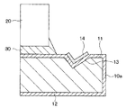
図1(a)は、本発明の第1実施形態に係る樹脂封止型の電子装置100の概略断面構成を示す図であり、図1(b)は、図1(a)中の電子装置100における丸で囲んだA部の拡大図である。
図9は、本発明の第2実施形態に係る電子装置の製造方法の要部を示す概略断面図である。
図10は、本発明の第3実施形態に係る電子装置の製造方法の要部を示す概略断面図である。なお、図10に示されている部位以外は、本実施形態の電子装置は、上記第1実施形態に示したものと同様にできる。
なお、上記の実施形態に示されるNi−Pメッキ膜などからなる下地メッキ膜10bは、必要に応じて設ければよいものであり、場合によっては、下地メッキ膜10bが無い構成であってもよい。
10b…下地メッキ膜としてのNi−P膜、11…ヒートシンクの一面、
12…ヒートシンクの他面、13…溝、14…樹脂材、20…配線基板、
30…接着剤、40…電子部品としてのICチップ、
41…電子部品としてのコンデンサ、80…モールド樹脂。
Claims (11)
- 電子部品(40、41)が実装された配線基板(20)を、ヒートシンク(10)の一面(11)上に搭載し、前記ヒートシンク(10)、前記電子部品(40、41)および前記配線基板(20)をモールド樹脂(80)により封止してなる電子装置において、
前記ヒートシンク(10)の表面のうち少なくとも前記モールド樹脂(80)と接する部位には、無電解メッキにてNiをメッキすることにより形成された無電解Niメッキ膜(10a)が形成されており、この無電解Niメッキ膜(10a)の表面は、凹凸形状を持つように粗化されていることを特徴とする電子装置。 - 前記無電解Niメッキ膜(10a)は、前記ヒートシンク(10)の表面のうち前記モールド樹脂(80)と接する部位のみに形成されていることを特徴とする請求項1に記載の電子装置。
- 前記無電解Niメッキ膜(10a)は、前記ヒートシンク(10)の表面のうち前記モールド樹脂(80)と接する部位および前記配線基板(20)が搭載される部位に形成されており、
前記配線基板(20)は、接着剤(30)を介して前記ヒートシンク(10)に搭載されていることを特徴とする請求項1に記載の電子装置。 - 前記ヒートシンク(10)の他面(12)が前記モールド樹脂(80)から露出しており、
前記無電解Niメッキ膜(10a)は、前記ヒートシンク(10)の表面のうち前記モールド樹脂(80)と接する部位および前記他面(12)に形成されていることを特徴とする請求項1に記載の電子装置。 - 前記無電解Niメッキ膜(10a)は、前記ヒートシンク(10)の表面の全面に形成されていることを特徴とする請求項1に記載の電子装置。
- 前記ヒートシンク(10)の表面と前記無電解Niメッキ膜(10a)との間には、前記無電解Niメッキ膜(10a)の下地となる下地メッキ膜(10b)が介在していることを特徴とする請求項1ないし5のいずれか1つに記載の電子装置。
- 前記下地メッキ膜(10b)は、Ni−Pメッキ膜であることを特徴とする請求項6に記載の電子装置。
- 前記無電解Niメッキ膜(10a)の凹凸形状は、針状突起を有する凹凸形状であることを特徴とする請求項1ないし7のいずれか1つに記載の電子装置。
- 電子部品(40、41)が搭載された配線基板(20)を、熱硬化性樹脂よりなる接着剤(30)を介してヒートシンク(10)の一面(11)上に搭載し、前記ヒートシンク(10)、前記電子部品(40、41)および前記配線基板(20)をモールド樹脂(80)により封止するようにした電子装置の製造方法において、
前記ヒートシンク(10)の表面のうち前記モールド樹脂(80)と接する部位および前記一面(11)に、無電解メッキにてNiをメッキすることにより形成され、その表面が凹凸形状を持つように粗化された無電解Niメッキ膜(10a)を設け、
前記配線基板(20)側に前記接着剤(30)を設け、前記ヒートシンク(10)を前記接着剤(30)の硬化温度以上に加熱した状態とし、
続いて、この加熱された状態にある前記ヒートシンク(10)の前記一面(11)上に前記接着剤(30)を介して前記配線基板(20)を搭載することで、前記ヒートシンク(10)の熱により、前記接着剤(30)を硬化させることを特徴とする電子装置の製造方法。 - 電子部品(40、41)が搭載された配線基板(20)を、接着剤(30)を介してヒートシンク(10)の一面(11)上に搭載し、前記ヒートシンク(10)、前記電子部品(40、41)および前記配線基板(20)をモールド樹脂(80)により封止するようにした電子装置の製造方法において、
前記ヒートシンク(10)の表面のうち前記モールド樹脂(80)と接する部位および前記一面(11)に、無電解メッキにてNiをメッキすることにより形成され、その表面が凹凸形状を持つように粗化された無電解Niメッキ膜(10a)を設け、
続いて、前記ヒートシンク(10)の前記一面(11)に位置する前記無電解Niメッキ膜(10a)の表面のうち前記接着剤(30)が設けられる部位の周囲を、前記モールド樹脂(80)と密着性を有する樹脂材(14)により被覆することで平滑化した後、
前記ヒートシンク(10)の前記一面(11)上に前記接着剤(30)を介して前記配線基板(20)を搭載することを特徴とする電子装置の製造方法。 - 前記ヒートシンク(10)の前記一面(11)のうち前記樹脂材(14)を設ける部位に、溝(13)を設けた後、
前記ヒートシンク(10)の表面のうち前記モールド樹脂(80)と接する部位および前記一面(11)に、前記無電解Niメッキ膜(10a)を設け、
続いて、前記無電解Niメッキ膜(10a)の表面のうち前記溝(13)内に位置する部位を、前記樹脂材(14)により被覆することを特徴とする電子装置の製造方法。
Priority Applications (1)
| Application Number | Priority Date | Filing Date | Title |
|---|---|---|---|
| JP2006015925A JP4591362B2 (ja) | 2006-01-25 | 2006-01-25 | 電子装置の製造方法 |
Applications Claiming Priority (1)
| Application Number | Priority Date | Filing Date | Title |
|---|---|---|---|
| JP2006015925A JP4591362B2 (ja) | 2006-01-25 | 2006-01-25 | 電子装置の製造方法 |
Publications (2)
| Publication Number | Publication Date |
|---|---|
| JP2007201036A true JP2007201036A (ja) | 2007-08-09 |
| JP4591362B2 JP4591362B2 (ja) | 2010-12-01 |
Family
ID=38455339
Family Applications (1)
| Application Number | Title | Priority Date | Filing Date |
|---|---|---|---|
| JP2006015925A Expired - Fee Related JP4591362B2 (ja) | 2006-01-25 | 2006-01-25 | 電子装置の製造方法 |
Country Status (1)
| Country | Link |
|---|---|
| JP (1) | JP4591362B2 (ja) |
Cited By (4)
| Publication number | Priority date | Publication date | Assignee | Title |
|---|---|---|---|---|
| JP2011059571A (ja) * | 2009-09-14 | 2011-03-24 | Sumitomo Electric Ind Ltd | 光サブアセンブリ |
| JP2016115806A (ja) * | 2014-12-15 | 2016-06-23 | トヨタ自動車株式会社 | 半導体装置 |
| EP2261933A4 (en) * | 2008-04-08 | 2018-03-28 | Murata Manufacturing Co. Ltd. | Capacitor and method for manufacturing the same |
| JP2018163962A (ja) * | 2017-03-24 | 2018-10-18 | 株式会社東芝 | 半導体装置及びその製造方法 |
Citations (3)
| Publication number | Priority date | Publication date | Assignee | Title |
|---|---|---|---|---|
| JP2003060137A (ja) * | 2001-08-08 | 2003-02-28 | Ibiden Co Ltd | モジュール用基板 |
| JP2004349497A (ja) * | 2003-05-22 | 2004-12-09 | Shinko Electric Ind Co Ltd | パッケージ部品及び半導体パッケージ |
| JP2005328018A (ja) * | 2004-04-14 | 2005-11-24 | Denso Corp | 半導体装置 |
-
2006
- 2006-01-25 JP JP2006015925A patent/JP4591362B2/ja not_active Expired - Fee Related
Patent Citations (3)
| Publication number | Priority date | Publication date | Assignee | Title |
|---|---|---|---|---|
| JP2003060137A (ja) * | 2001-08-08 | 2003-02-28 | Ibiden Co Ltd | モジュール用基板 |
| JP2004349497A (ja) * | 2003-05-22 | 2004-12-09 | Shinko Electric Ind Co Ltd | パッケージ部品及び半導体パッケージ |
| JP2005328018A (ja) * | 2004-04-14 | 2005-11-24 | Denso Corp | 半導体装置 |
Cited By (4)
| Publication number | Priority date | Publication date | Assignee | Title |
|---|---|---|---|---|
| EP2261933A4 (en) * | 2008-04-08 | 2018-03-28 | Murata Manufacturing Co. Ltd. | Capacitor and method for manufacturing the same |
| JP2011059571A (ja) * | 2009-09-14 | 2011-03-24 | Sumitomo Electric Ind Ltd | 光サブアセンブリ |
| JP2016115806A (ja) * | 2014-12-15 | 2016-06-23 | トヨタ自動車株式会社 | 半導体装置 |
| JP2018163962A (ja) * | 2017-03-24 | 2018-10-18 | 株式会社東芝 | 半導体装置及びその製造方法 |
Also Published As
| Publication number | Publication date |
|---|---|
| JP4591362B2 (ja) | 2010-12-01 |
Similar Documents
| Publication | Publication Date | Title |
|---|---|---|
| JP5387685B2 (ja) | 半導体装置の製造方法 | |
| JP2008172172A (ja) | 電子制御装置及びその製造方法 | |
| JP2006100752A (ja) | 回路装置およびその製造方法 | |
| JP4967701B2 (ja) | 電力半導体装置 | |
| JPH0883861A (ja) | 半導体パッケージ被覆用金属箔材料および半導体装置 | |
| JP5126201B2 (ja) | 半導体モジュールおよびその製造方法 | |
| JP2006253354A (ja) | 回路装置およびその製造方法 | |
| JP5262983B2 (ja) | モールドパッケージおよびその製造方法 | |
| JP4591362B2 (ja) | 電子装置の製造方法 | |
| JP2009267344A (ja) | 半導体装置の製造方法 | |
| JP3606078B2 (ja) | 半導体装置およびその製造方法 | |
| JP2000236060A (ja) | 半導体装置 | |
| JP2008211168A (ja) | 半導体装置および半導体モジュール | |
| JP2006191143A (ja) | 半導体装置 | |
| JP5035356B2 (ja) | 樹脂封止型電子装置およびその製造方法 | |
| JP5083076B2 (ja) | 電子装置の製造方法 | |
| JP2010141158A (ja) | 電子装置 | |
| JP2015106649A (ja) | 電子装置 | |
| JP2008258435A (ja) | 半導体装置及びその製造方法 | |
| CN209880589U (zh) | 半导体封装结构 | |
| JP2010199516A (ja) | 電子装置 | |
| TWM545363U (zh) | 晶片封裝結構 | |
| JP2008147267A (ja) | 半導体装置とその製造方法、および放熱板付きリードフレーム | |
| JP2008288566A (ja) | 半導体装置 | |
| TWI591707B (zh) | 薄型化晶片之封裝結構及其製造方法 |
Legal Events
| Date | Code | Title | Description |
|---|---|---|---|
| A621 | Written request for application examination |
Free format text: JAPANESE INTERMEDIATE CODE: A621 Effective date: 20080204 |
|
| A977 | Report on retrieval |
Free format text: JAPANESE INTERMEDIATE CODE: A971007 Effective date: 20100125 |
|
| A131 | Notification of reasons for refusal |
Free format text: JAPANESE INTERMEDIATE CODE: A131 Effective date: 20100209 |
|
| A521 | Request for written amendment filed |
Free format text: JAPANESE INTERMEDIATE CODE: A523 Effective date: 20100329 |
|
| A131 | Notification of reasons for refusal |
Free format text: JAPANESE INTERMEDIATE CODE: A131 Effective date: 20100518 |
|
| A521 | Request for written amendment filed |
Free format text: JAPANESE INTERMEDIATE CODE: A523 Effective date: 20100709 |
|
| TRDD | Decision of grant or rejection written | ||
| A01 | Written decision to grant a patent or to grant a registration (utility model) |
Free format text: JAPANESE INTERMEDIATE CODE: A01 Effective date: 20100817 |
|
| A01 | Written decision to grant a patent or to grant a registration (utility model) |
Free format text: JAPANESE INTERMEDIATE CODE: A01 |
|
| A61 | First payment of annual fees (during grant procedure) |
Free format text: JAPANESE INTERMEDIATE CODE: A61 Effective date: 20100830 |
|
| FPAY | Renewal fee payment (event date is renewal date of database) |
Free format text: PAYMENT UNTIL: 20130924 Year of fee payment: 3 |
|
| R151 | Written notification of patent or utility model registration |
Ref document number: 4591362 Country of ref document: JP Free format text: JAPANESE INTERMEDIATE CODE: R151 |
|
| FPAY | Renewal fee payment (event date is renewal date of database) |
Free format text: PAYMENT UNTIL: 20130924 Year of fee payment: 3 |
|
| R250 | Receipt of annual fees |
Free format text: JAPANESE INTERMEDIATE CODE: R250 |
|
| R250 | Receipt of annual fees |
Free format text: JAPANESE INTERMEDIATE CODE: R250 |
|
| R250 | Receipt of annual fees |
Free format text: JAPANESE INTERMEDIATE CODE: R250 |
|
| R250 | Receipt of annual fees |
Free format text: JAPANESE INTERMEDIATE CODE: R250 |
|
| R250 | Receipt of annual fees |
Free format text: JAPANESE INTERMEDIATE CODE: R250 |
|
| LAPS | Cancellation because of no payment of annual fees |