JP2007201036A - Electronic device and its manufacturing process - Google Patents
Electronic device and its manufacturing process Download PDFInfo
- Publication number
- JP2007201036A JP2007201036A JP2006015925A JP2006015925A JP2007201036A JP 2007201036 A JP2007201036 A JP 2007201036A JP 2006015925 A JP2006015925 A JP 2006015925A JP 2006015925 A JP2006015925 A JP 2006015925A JP 2007201036 A JP2007201036 A JP 2007201036A
- Authority
- JP
- Japan
- Prior art keywords
- heat sink
- electroless
- plating film
- mold resin
- electronic device
- Prior art date
- Legal status (The legal status is an assumption and is not a legal conclusion. Google has not performed a legal analysis and makes no representation as to the accuracy of the status listed.)
- Granted
Links
Images


Classifications
-
- H—ELECTRICITY
- H01—ELECTRIC ELEMENTS
- H01L—SEMICONDUCTOR DEVICES NOT COVERED BY CLASS H10
- H01L2224/00—Indexing scheme for arrangements for connecting or disconnecting semiconductor or solid-state bodies and methods related thereto as covered by H01L24/00
- H01L2224/01—Means for bonding being attached to, or being formed on, the surface to be connected, e.g. chip-to-package, die-attach, "first-level" interconnects; Manufacturing methods related thereto
- H01L2224/42—Wire connectors; Manufacturing methods related thereto
- H01L2224/47—Structure, shape, material or disposition of the wire connectors after the connecting process
- H01L2224/48—Structure, shape, material or disposition of the wire connectors after the connecting process of an individual wire connector
- H01L2224/4805—Shape
- H01L2224/4809—Loop shape
- H01L2224/48091—Arched
-
- H—ELECTRICITY
- H01—ELECTRIC ELEMENTS
- H01L—SEMICONDUCTOR DEVICES NOT COVERED BY CLASS H10
- H01L2224/00—Indexing scheme for arrangements for connecting or disconnecting semiconductor or solid-state bodies and methods related thereto as covered by H01L24/00
- H01L2224/01—Means for bonding being attached to, or being formed on, the surface to be connected, e.g. chip-to-package, die-attach, "first-level" interconnects; Manufacturing methods related thereto
- H01L2224/42—Wire connectors; Manufacturing methods related thereto
- H01L2224/47—Structure, shape, material or disposition of the wire connectors after the connecting process
- H01L2224/48—Structure, shape, material or disposition of the wire connectors after the connecting process of an individual wire connector
- H01L2224/481—Disposition
- H01L2224/48151—Connecting between a semiconductor or solid-state body and an item not being a semiconductor or solid-state body, e.g. chip-to-substrate, chip-to-passive
- H01L2224/48221—Connecting between a semiconductor or solid-state body and an item not being a semiconductor or solid-state body, e.g. chip-to-substrate, chip-to-passive the body and the item being stacked
- H01L2224/48225—Connecting between a semiconductor or solid-state body and an item not being a semiconductor or solid-state body, e.g. chip-to-substrate, chip-to-passive the body and the item being stacked the item being non-metallic, e.g. insulating substrate with or without metallisation
- H01L2224/48227—Connecting between a semiconductor or solid-state body and an item not being a semiconductor or solid-state body, e.g. chip-to-substrate, chip-to-passive the body and the item being stacked the item being non-metallic, e.g. insulating substrate with or without metallisation connecting the wire to a bond pad of the item
-
- H—ELECTRICITY
- H01—ELECTRIC ELEMENTS
- H01L—SEMICONDUCTOR DEVICES NOT COVERED BY CLASS H10
- H01L2224/00—Indexing scheme for arrangements for connecting or disconnecting semiconductor or solid-state bodies and methods related thereto as covered by H01L24/00
- H01L2224/01—Means for bonding being attached to, or being formed on, the surface to be connected, e.g. chip-to-package, die-attach, "first-level" interconnects; Manufacturing methods related thereto
- H01L2224/42—Wire connectors; Manufacturing methods related thereto
- H01L2224/47—Structure, shape, material or disposition of the wire connectors after the connecting process
- H01L2224/49—Structure, shape, material or disposition of the wire connectors after the connecting process of a plurality of wire connectors
- H01L2224/4901—Structure
- H01L2224/4903—Connectors having different sizes, e.g. different diameters
-
- H—ELECTRICITY
- H01—ELECTRIC ELEMENTS
- H01L—SEMICONDUCTOR DEVICES NOT COVERED BY CLASS H10
- H01L2224/00—Indexing scheme for arrangements for connecting or disconnecting semiconductor or solid-state bodies and methods related thereto as covered by H01L24/00
- H01L2224/73—Means for bonding being of different types provided for in two or more of groups H01L2224/10, H01L2224/18, H01L2224/26, H01L2224/34, H01L2224/42, H01L2224/50, H01L2224/63, H01L2224/71
- H01L2224/732—Location after the connecting process
- H01L2224/73251—Location after the connecting process on different surfaces
- H01L2224/73265—Layer and wire connectors
-
- H—ELECTRICITY
- H01—ELECTRIC ELEMENTS
- H01L—SEMICONDUCTOR DEVICES NOT COVERED BY CLASS H10
- H01L2224/00—Indexing scheme for arrangements for connecting or disconnecting semiconductor or solid-state bodies and methods related thereto as covered by H01L24/00
- H01L2224/91—Methods for connecting semiconductor or solid state bodies including different methods provided for in two or more of groups H01L2224/80 - H01L2224/90
- H01L2224/92—Specific sequence of method steps
- H01L2224/922—Connecting different surfaces of the semiconductor or solid-state body with connectors of different types
- H01L2224/9222—Sequential connecting processes
- H01L2224/92242—Sequential connecting processes the first connecting process involving a layer connector
- H01L2224/92247—Sequential connecting processes the first connecting process involving a layer connector the second connecting process involving a wire connector
-
- H—ELECTRICITY
- H01—ELECTRIC ELEMENTS
- H01L—SEMICONDUCTOR DEVICES NOT COVERED BY CLASS H10
- H01L2924/00—Indexing scheme for arrangements or methods for connecting or disconnecting semiconductor or solid-state bodies as covered by H01L24/00
- H01L2924/19—Details of hybrid assemblies other than the semiconductor or other solid state devices to be connected
- H01L2924/191—Disposition
- H01L2924/19101—Disposition of discrete passive components
- H01L2924/19105—Disposition of discrete passive components in a side-by-side arrangement on a common die mounting substrate
-
- H—ELECTRICITY
- H01—ELECTRIC ELEMENTS
- H01L—SEMICONDUCTOR DEVICES NOT COVERED BY CLASS H10
- H01L2924/00—Indexing scheme for arrangements or methods for connecting or disconnecting semiconductor or solid-state bodies as covered by H01L24/00
- H01L2924/19—Details of hybrid assemblies other than the semiconductor or other solid state devices to be connected
- H01L2924/191—Disposition
- H01L2924/19101—Disposition of discrete passive components
- H01L2924/19107—Disposition of discrete passive components off-chip wires
Abstract
Description
本発明は、電子部品が実装された配線基板を放熱用のヒートシンク上に搭載し、これらをモールド樹脂にて封止してなる電子装置、いわゆる樹脂封止型の電子装置および、そのような樹脂封止型の電子装置の製造方法に関する。 The present invention provides an electronic device in which a wiring board on which electronic components are mounted is mounted on a heat sink for heat dissipation and is sealed with a mold resin, a so-called resin-sealed electronic device, and such a resin. The present invention relates to a method for manufacturing a sealed electronic device.
従来より、この種の電子装置としては、電子部品が実装された配線基板を、ヒートシンクの一面上に搭載し、ヒートシンク、電子部品および配線基板をモールド樹脂により封止してなるものが提案されている(特許文献1参照)。 Conventionally, as this type of electronic device, a device in which a wiring board on which electronic components are mounted is mounted on one surface of a heat sink, and the heat sink, the electronic component, and the wiring substrate are sealed with a mold resin has been proposed. (See Patent Document 1).
このような電子装置は、一般に、電子部品が搭載された配線基板を、接着剤を介してヒートシンクの一面上に搭載した後、トランスファーモールド法により樹脂封止を行うことで製造される。
しかしながら、このような樹脂封止型の電子装置は、冷熱サイクルや電子装置を外部基材へ実装する時のはんだリフローなどにより生じる熱応力によって、ヒートシンクとモールド樹脂との間に剥離が生じやすい。これは、金属からなるヒートシンクと樹脂との熱膨張係数の差が大きいためである。 However, in such a resin-encapsulated electronic device, peeling between the heat sink and the mold resin is likely to occur due to thermal stress generated by a cooling cycle or solder reflow when the electronic device is mounted on an external substrate. This is because the difference in coefficient of thermal expansion between the heat sink made of metal and the resin is large.
そして、上記したモールド樹脂とヒートシンクとの剥離が生じると、モールド樹脂の内部において樹脂クラックが発生し、これがモールド樹脂の外部にまで到達するという問題が発生する。 When the mold resin and the heat sink are peeled off, a resin crack is generated inside the mold resin, which causes a problem that it reaches the outside of the mold resin.
本発明は、上記問題に鑑みてなされたものであり、ヒートシンクをモールド樹脂により封止してなる樹脂封止型の電子装置において、ヒートシンクとモールド樹脂との剥離を抑制することを目的とする。 The present invention has been made in view of the above problems, and an object of the present invention is to suppress peeling between a heat sink and a mold resin in a resin-sealed electronic device in which a heat sink is sealed with a mold resin.
上記目的を達成するため、本発明者は、ヒートシンクとモールド樹脂との接触部において、ヒートシンクとモールド樹脂との密着力を向上させることに着目し、鋭意検討を行い、本発明を創出するに至った。 In order to achieve the above-mentioned object, the present inventor has focused on improving the adhesion between the heat sink and the mold resin at the contact portion between the heat sink and the mold resin, and intensively studied and led to the creation of the present invention. It was.
すなわち、本発明は、ヒートシンク(10)の表面のうち少なくとも前記モールド樹脂(80)と接する部位に、無電解メッキにてNiをメッキすることにより形成された無電解Niメッキ膜(10a)を形成するとともに、この無電解Niメッキ膜(10a)の表面を、凹凸形状を持つように粗化されたものとしたことを、第1の特徴とする。 That is, the present invention forms an electroless Ni plating film (10a) formed by plating Ni by electroless plating on at least a portion of the surface of the heat sink (10) that contacts the mold resin (80). In addition, the first feature is that the surface of the electroless Ni plating film (10a) is roughened so as to have an uneven shape.
それによれば、ヒートシンク(10)の表面のうちモールド樹脂(80)と接する部位では、当該部位に設けられている無電解Niメッキ膜(10a)が凹凸形状を持つように粗化されているため、モールド樹脂(80)との密着性が向上し、ヒートシンク(10)とモールド樹脂(80)との剥離を抑制することができる。 According to this, the portion of the surface of the heat sink (10) in contact with the mold resin (80) is roughened so that the electroless Ni plating film (10a) provided in the portion has an uneven shape. Adhesion with the mold resin (80) is improved, and peeling between the heat sink (10) and the mold resin (80) can be suppressed.
こような構成においては、無電解Niメッキ膜(10a)は、ヒートシンク(10)の表面のうちモールド樹脂(80)と接する部位のみに形成されていてもよい。 In such a configuration, the electroless Ni plating film (10a) may be formed only on the surface of the heat sink (10) that is in contact with the mold resin (80).
また、このような構成においては、無電解Niメッキ膜(10a)は、ヒートシンク(10)の表面のうちモールド樹脂(80)と接する部位および配線基板(20)が搭載される部位に形成されており、配線基板(20)は、接着剤(30)を介してヒートシンク(10)に搭載されているものにできる。 Further, in such a configuration, the electroless Ni plating film (10a) is formed on the surface of the heat sink (10) in a portion in contact with the mold resin (80) and a portion on which the wiring board (20) is mounted. The wiring board (20) can be mounted on the heat sink (10) via an adhesive (30).
このように、配線基板(20)を、接着剤(30)を介してヒートシンク(10)に搭載する場合に、当該搭載部位に上記の粗化された無電解Niメッキ膜(10a)を設けることで、当該無電解Niメッキ膜(10a)と接着剤(30)との密着性の向上が可能になる。 Thus, when the wiring board (20) is mounted on the heat sink (10) via the adhesive (30), the roughened electroless Ni plating film (10a) is provided on the mounting portion. Thus, the adhesion between the electroless Ni plating film (10a) and the adhesive (30) can be improved.
また、このような構成においては、ヒートシンク(10)の他面(12)がモールド樹脂(80)から露出しており、無電解Niメッキ膜(10a)は、ヒートシンク(10)の表面のうちモールド樹脂(80)と接する部位および他面(12)に形成されているものにできる。 Further, in such a configuration, the other surface (12) of the heat sink (10) is exposed from the mold resin (80), and the electroless Ni plating film (10a) is molded on the surface of the heat sink (10). It can be formed on the part in contact with the resin (80) and the other surface (12).
このように、ヒートシンク(10)の表面のうちモールド樹脂(80)から露出する他面(12)に、上記の粗化された無電解Niメッキ膜(10a)を設ければ、この他面(12)に接着剤などを介して外部基材を接触させ、放熱を図るような場合に、当該外部部材との密着性の向上が可能になる。 Thus, if the roughened electroless Ni plating film (10a) is provided on the other surface (12) exposed from the mold resin (80) in the surface of the heat sink (10), this other surface ( In the case where the external base material is brought into contact with 12) via an adhesive or the like to dissipate heat, the adhesion to the external member can be improved.
さらに、このような構成においては、無電解Niメッキ膜(10a)を、ヒートシンク(10)の表面の全面に形成すれば、上記したモールド樹脂(80)の剥離抑制、配線基板(20)を搭載する接着剤(30)との密着性向上、および、外部基材との密着性向上といった各効果が期待できる。 Further, in such a configuration, if the electroless Ni plating film (10a) is formed on the entire surface of the heat sink (10), the mold resin (80) is prevented from being peeled off and the wiring board (20) is mounted. Various effects such as improvement in adhesion with the adhesive (30) to be performed and improvement in adhesion with the external substrate can be expected.
また、このような構成において、ヒートシンク(10)の表面と無電解Niメッキ膜(10a)との間に、無電解Niメッキ膜(10a)の下地となる下地メッキ膜(10b)を介在させれば、粗化された無電解Niメッキ膜(10a)はピンホールなどが発生しやすいため、この下地メッキ膜(10b)によって、その下のヒートシンク(10)の露出が防止できる。 In such a configuration, a base plating film (10b) serving as a base of the electroless Ni plating film (10a) can be interposed between the surface of the heat sink (10) and the electroless Ni plating film (10a). For example, since the rough electroless Ni plating film (10a) is likely to generate pinholes, the underlying plating film (10b) can prevent the heat sink (10) underneath from being exposed.
また、この場合において、下地メッキ膜(10b)としてNi−Pメッキ膜を用いれば、無電解Niメッキ膜(10a)とヒートシンク(10)との密着性を向上させることができる。 In this case, if a Ni—P plating film is used as the base plating film (10b), the adhesion between the electroless Ni plating film (10a) and the heat sink (10) can be improved.
また、電子部品(40、41)が搭載された配線基板(20)を、熱硬化性樹脂などよりなる接着剤(30)を介してヒートシンク(10)の一面(11)上に搭載する場合において、このヒートシンク(10)の一面(11)に、粗化された無電解Niメッキ膜(10a)を設けるとき、この無電解メッキ膜(10a)は、熱硬化性樹脂などよりなる接着剤(30)の低分子成分に対する濡れ性がよいものであるため、ブリードが発生しやすくなる。 In the case where the wiring board (20) on which the electronic components (40, 41) are mounted is mounted on one surface (11) of the heat sink (10) via an adhesive (30) made of a thermosetting resin or the like. When a roughened electroless Ni plating film (10a) is provided on one surface (11) of the heat sink (10), the electroless plating film (10a) is formed of an adhesive (30 ) Is easy to bleed because of its good wettability to low molecular components.
このブリードが発生すると、ヒートシンク(10)の一面(11)のうち配線基板(20)の搭載領域よりも外側に上記した低分子成分が広がり、ヒートシンク(10)とモールド樹脂(80)との密着性を低下させやすくなる。 When this bleed occurs, the low molecular component described above spreads outside the mounting area of the wiring board (20) on one surface (11) of the heat sink (10), and the heat sink (10) and the mold resin (80) are in close contact with each other. It becomes easy to reduce the nature.
そこで、本発明は、このブリード抑制を考慮して、配線基板(20)を、熱硬化性樹脂よりなる接着剤(30)を介してヒートシンク(10)の一面(11)上に搭載する製造方法において、ヒートシンク(10)の表面のうちモールド樹脂(80)と接する部位および一面(11)に、無電解メッキにてNiをメッキすることにより形成され、その表面が凹凸形状を持つように粗化された無電解Niメッキ膜(10a)を設け、配線基板(20)側に接着剤(30)を設け、ヒートシンク(10)を接着剤(30)の硬化温度以上に加熱した状態とし、続いて、この加熱された状態にあるヒートシンク(10)の一面(11)上に接着剤(30)を介して配線基板(20)を搭載することで、ヒートシンク(10)の熱により、接着剤(30)を硬化させることを、第2の特徴とする。 Therefore, the present invention considers this bleed suppression and a manufacturing method for mounting the wiring board (20) on one surface (11) of the heat sink (10) via an adhesive (30) made of a thermosetting resin. The surface of the heat sink (10) in contact with the mold resin (80) and one surface (11) are formed by plating Ni by electroless plating and roughened so that the surface has an uneven shape. The electroless Ni plating film (10a) is provided, the adhesive (30) is provided on the wiring substrate (20) side, and the heat sink (10) is heated to a temperature equal to or higher than the curing temperature of the adhesive (30). By mounting the wiring board (20) on the one surface (11) of the heat sink (10) in the heated state via the adhesive (30), the heat of the heat sink (10) causes the adhesive (3 Curing the), the second feature.
それによれば、接着剤(30)は、配線基板(20)の搭載と同時に硬化を始めるため、ブリードの進展を抑制できる。 According to this, since the adhesive (30) starts to be cured simultaneously with the mounting of the wiring board (20), the progress of bleeding can be suppressed.
また、本発明は、このブリード抑制を考慮して、配線基板(20)を、接着剤(30)を介してヒートシンク(10)の一面(11)上に搭載する製造方法において、ヒートシンク(10)の表面のうちモールド樹脂(80)と接する部位および一面(11)に、上記無電解Niメッキ膜(10a)を設け、続いて、ヒートシンク(10)の一面(11)に位置する無電解Niメッキ膜(10a)の表面のうち接着剤(30)が設けられる部位の周囲を、モールド樹脂(80)と密着性を有する樹脂材(14)により被覆することで平滑化した後、ヒートシンク(10)の一面(11)上に接着剤(30)を介して配線基板(20)を搭載することを、第3の特徴とする。 In addition, in consideration of this bleed suppression, the present invention provides a heat sink (10) in a manufacturing method in which a wiring board (20) is mounted on one surface (11) of a heat sink (10) via an adhesive (30). The electroless Ni plating film (10a) is provided on the surface and the surface (11) in contact with the mold resin (80), and then the electroless Ni plating located on the surface (11) of the heat sink (10). The surface of the surface of the film (10a) is smoothed by covering the periphery of the portion where the adhesive (30) is provided with the resin material (14) having adhesiveness with the mold resin (80), and then the heat sink (10). A third feature is that the wiring board (20) is mounted on the one surface (11) via the adhesive (30).
それによれば、樹脂材(14)の表面は無電解Niメッキ膜(10a)に比べて平滑化されるため、ブリードの進展を抑制できる。 According to this, since the surface of the resin material (14) is smoothed compared to the electroless Ni plating film (10a), the progress of bleeding can be suppressed.
このような製造方法において、ヒートシンク(10)の一面(11)のうち樹脂材(14)を設ける部位に、溝(13)を設けた後、ヒートシンク(10)の表面のうちモールド樹脂(80)と接する部位および一面(11)に、無電解Niメッキ膜(10a)を設け、続いて、無電解Niメッキ膜(10a)の表面のうち溝(13)内に位置する部位を、樹脂材(14)により被覆するようにすれば、溝(13)により樹脂材(14)の塗布が容易になる。 In such a manufacturing method, after providing the groove (13) in a portion of the surface (11) of the heat sink (10) where the resin material (14) is provided, the mold resin (80) of the surface of the heat sink (10) is provided. An electroless Ni plating film (10a) is provided on the part and one surface (11) in contact with each other, and subsequently, a part of the surface of the electroless Ni plating film (10a) located in the groove (13) If it covers by 14), application | coating of the resin material (14) will become easy by a groove | channel (13).
なお、特許請求の範囲およびこの欄で記載した各手段の括弧内の符号は、後述する実施形態に記載の具体的手段との対応関係を示す一例である。 In addition, the code | symbol in the parenthesis of each means described in a claim and this column is an example which shows a corresponding relationship with the specific means as described in embodiment mentioned later.
以下、本発明の実施形態について図に基づいて説明する。なお、以下の各実施形態相互において、互いに同一もしくは均等である部分には、説明の簡略化を図るべく、図中、同一符号を付してある。 Hereinafter, embodiments of the present invention will be described with reference to the drawings. In the following embodiments, parts that are the same or equivalent to each other are given the same reference numerals in the drawings in order to simplify the description.
(第1実施形態)
図1(a)は、本発明の第1実施形態に係る樹脂封止型の電子装置100の概略断面構成を示す図であり、図1(b)は、図1(a)中の電子装置100における丸で囲んだA部の拡大図である。
(First embodiment)
FIG. 1A is a diagram showing a schematic cross-sectional configuration of a resin-encapsulated
本電子装置100はヒートシンク10を備えており、このヒートシンク10は、Fe、Cu、Mo、42アロイ、コバールなどの金属など、放熱性に優れた材料からなるものであり、たとえば矩形板状をなす。特に限定するものではないが、本例では、ヒートシンク10はFe板からなる。
The
このヒートシンク10の一面11上には、セラミック基板やプリント基板などからなる配線基板20が搭載されている。ここでは、配線基板20は、ヒートシンク10よりも一回り小さい、たとえば矩形板状のものである。
On one
そして、配線基板20とヒートシンク10との間には、シリコン系樹脂やエポキシ系樹脂などの熱硬化性樹脂などよりなる接着剤30が介在しており、配線基板20とヒートシンク10とは、この接着剤30を介して接着されている。
An adhesive 30 made of a thermosetting resin such as a silicon resin or an epoxy resin is interposed between the
また、配線基板20には、ICチップ40やコンデンサ41などの各種の電子部品40、41が実装されている。
Various
ICチップ40は、シリコン基板などからなるもので、半導体プロセス技術を用いてトランジスタなどの素子が形成されたものであり、はんだや導電性接着剤などの接合材50を介して配線基板20の上に固定されるとともに、金やアルミニウムなどからなるボンディングワイヤ60を介して、配線基板20と電気的に接続されている。
The
また、コンデンサ41も、上記接合材50を介して配線基板20の上に、電気的・機械的に接続されている。なお、配線基板20には、これらICチップ40およびコンデンサ41以外の部品が実装されていてもよい。
The
また、ヒートシンク10および配線基板20の周囲には、Cuや42アロイ合金などの金属からなるリードとしてのリードフレーム70が配置されている。そして、配線基板20とリードフレーム70とは、ボンディングワイヤ60によって結線され電気的に接続されている。
A
そして、これらヒートシンク10、電子部品40、41、配線基板20、リードフレーム70およびボンディングワイヤ60は、モールド樹脂80によって包み込まれるように封止されている。
The
ここで、本実施形態では、ヒートシンク10のうち配線基板20が搭載される面である上記一面11とは反対側の他面12を、モールド樹脂80から露出させており、それによって、放熱性の向上を図っている。
Here, in the present embodiment, the
このモールド樹脂80は、エポキシ系樹脂などの通常のモールド材料からなるものであり、一般的なトランスファーモールド法により形成されるものである。たとえば、モールド樹脂80は、エポキシ系樹脂からなり、さらに熱膨張係数を調整する等のためにシリカなどからなるフィラーが含有されたものである。
The
このような電子装置100において、本実施形態では、ヒートシンク10の表面のうち少なくともモールド樹脂80と接する部位に、図1に示される例では、ヒートシンク10の表面の全面に、無電解Niメッキ膜10aが形成されている。
In such an
この無電解Niメッキ膜10aは、無電解メッキにてNiをメッキすることにより形成されており、図1(b)に示されるように、この無電解Niメッキ膜10aの表面は、凹凸形状を持つように粗化されている。
The electroless
また、図1(b)に示されるように、ヒートシンク10の表面と無電解Niメッキ膜10aとの間には、無電解Niメッキ膜10aの下地となる下地メッキ膜10bが介在している。なお、図1(a)では下地メッキ膜10bは省略してある。
Further, as shown in FIG. 1B, a
この下地メッキ膜10bは、Ni−Pメッキ膜やNi−Bメッキ膜などからなる。特に限定するものではないが、本例では、下地メッキ膜10bはNi−Pメッキ膜10bよりなる。
The
ここで、Ni−Pメッキ膜10bは、一般的な無電解Ni−Pメッキ浴、メッキ条件でメッキすることで形成される。また、その上に設けられる表面が粗化された無電解Niメッキ膜10aは、無電解メッキ法によって形成される。たとえば、Ni−Pメッキ膜10b、無電解Niメッキ膜10aの膜厚は、それぞれ、※ である。
Here, the Ni-
本例では、無電解Niメッキ膜10aは、図1(b)に示されるように、針状突起を有する凹凸形状となっている。この無電解Niメッキ膜10aの形成方法は公知であり、たとえば、Niメッキのメッキ成膜時に薬液成分などのメッキ条件を調整することなどにより、粗化を行うことができる。
In this example, the electroless
この無電解Niメッキ膜10aの粗化レベルは、モールド樹脂80との密着性を満足するために、本例では比表面積2.3以上が好ましい。この比表面積とは、原子間力顕微鏡(AFM)で測定した値であり、無電解Niメッキ膜10aの表面における所定の単位面積をAFMで測定し、その画像解析などを行うことで求められるものであり、樹脂密着性を表すのに最も適した特性値である。
In order to satisfy the adhesiveness with the
また、この無電解Niメッキ膜10aの種々の表面粗化状態を図2〜図7に示す。図2、図4、図6は、それぞれ表面粗化状態の異なる無電解Niメッキ膜10aの表面を電子顕微鏡で観察したときの顕微鏡写真を示す図であり、図3、図5、図7は、それぞれ図2、図4、図6の各状態となっている無電解Niメッキ膜10aの断面構成を模式的に示す図である。
Various surface roughening states of the electroless
無電解Niメッキ膜10aの表面形状は、図2、図3に示されるような丸みを帯びた凹凸形状でもよいが、図4および図5、または、図6および図7に示されるような針状形状の凹凸形状の方が、よりモールド樹脂80との密着力に優れる。
The surface shape of the electroless
図4および図5では、図2および図3に比べて無電解Niメッキ膜10aの比表面積が増えるものであり、図6および図7では、針が様々な方向に向いていることで、無電解Niメッキ膜10aとモールド樹脂80との密着力が増加する。これら図2〜図7に示される無電解Niメッキ膜10aの表面形状は、当業者であれば、薬液成分などのメッキ条件を調整することなどにより実現できる。
4 and 5, the specific surface area of the electroless
このような電子装置100は、次のような一般的な製造方法により製造することができる。まず、配線基板20に、上記接合材50を介して電子部品40、41を搭載する。一方で、上記メッキ膜10a、10bが形成されたヒートシンク10を用意する。
Such an
そして、この電子部品40、41が搭載された配線基板20を、熱硬化性樹脂などよりなる接着剤30を介してヒートシンク10の一面11上に搭載し、リードフレーム70と配線基板20との間や配線基板20とICチップ40との間でワイヤボンディングを行った後、このものをモールド樹脂80にて封止する。こうして、本電子装置100が製造される。
Then, the
ところで、本実施形態によれば、このような樹脂封止型の電子装置100において、ヒートシンク10の表面のうちモールド樹脂80と接する部位に、粗化された無電解Niメッキ膜10aが形成されている。
By the way, according to the present embodiment, in such a resin-encapsulated
それによれば、ヒートシンク10の表面のうちモールド樹脂80と接する部位では、ヒートシンク10の当該部位に設けられている無電解Niメッキ膜10aの表面が凹凸形状を持つように粗化されているため、この凹凸部分によって無電解Niメッキ膜10aとモールド樹脂80との間において、接触面積の増大やアンカー効果などの作用を期待することができる。
According to this, in the part of the surface of the
このことにより、ヒートシンク10とモールド樹脂80との密着性が向上し、ヒートシンク10からのモールド樹脂80の剥離を抑制することができる。そして、結果的に、モールド樹脂80の内部から外部へ到達する樹脂クラックなど、樹脂剥離に伴う不具合の防止がなされ、信頼性が向上する。
Thereby, the adhesiveness between the
ここで、図1に示される例では、無電解Niメッキ膜10aは、ヒートシンク10の表面の全面に形成されているが、上記した効果を奏するためには、無電解Niメッキ膜10aは、ヒートシンク10の表面のうち少なくともモールド樹脂80と接する部位に形成されていればよい。
Here, in the example shown in FIG. 1, the electroless
たとえば、図8に示されるように、無電解Niメッキ膜10aは、ヒートシンク10の表面のうちモールド樹脂80と接する部位のみに形成されていてもよい。図8に示される例では、ヒートシンク10の表面のうち一面11における接着剤30が配置される部位を除く部位と、側面とに無電解Niメッキ膜10aが形成されている。
For example, as shown in FIG. 8, the electroless
また、本実施形態の電子装置100のように、配線基板20が接着剤30を介してヒートシンク10に搭載されている場合、無電解Niメッキ膜10aは、ヒートシンク10の表面のうちモールド樹脂80と接する部位および配線基板20が搭載される部位にのみ形成されていてもよい。
Further, when the
ここで、ヒートシンク10の表面のうち配線基板20が搭載される部位とは、図1に示される電子装置100においては、ヒートシンク10の一面11における接着剤30が配置される部位である。
Here, the portion of the surface of the
このように、配線基板20を、接着剤30を介してヒートシンク10に搭載する場合に、当該搭載部位に粗化された無電解Niメッキ膜10aを設けることで、当該無電解Niメッキ膜10aと接着剤30との密着性の向上が可能になる。
Thus, when the
これは、粗化された無電解Niメッキ膜10aでは接着剤30の濡れ性が向上するなどの理由によるものであり、その結果、配線基板20の剥離防止効果が期待され、信頼性が向上する。
This is for the reason that the wettability of the adhesive 30 is improved in the roughened electroless
また、本実施形態の電子装置100のように、ヒートシンク10の他面12がモールド樹脂80から露出しているハーフモールドタイプの場合には、無電解Niメッキ膜10aは、ヒートシンク10の表面のうちモールド樹脂80と接する部位および当該他面12にのみ、形成されていてもよい。
In the case of a half mold type in which the
このようなハーフモールドタイプの電子装置100の場合、ヒートシンク10のうちモールド樹脂80から露出する面すなわち他面を、接着剤や熱伝導性グリスなどを介して、冷却器などの外部基材に接触させ、それによって、電子装置100における放熱の促進を図ることが多い。
In the case of such a half mold type
そこで、このように、ヒートシンク10の表面のうちモールド樹脂80から露出する他面12に、粗化された無電解Niメッキ膜10aを設ければ、この他面12に接着剤などを介して外部基材を接触させ、放熱を図るような場合に、当該外部基材との密着性の向上が可能になる。その結果、外部基材に対するヒートシンクの接着力の向上効果が期待され、信頼性が向上する。
Therefore, if the roughened electroless
また、上述したように、本実施形態では、無電解Niメッキ膜10aは、ヒートシンク10の表面の全面に形成されている。
Further, as described above, in the present embodiment, the electroless
それによれば、無電解Niメッキ膜10aを、ヒートシンク10の表面のうちモールド樹脂80と接する部位に形成したことによるモールド樹脂80の剥離抑制効果、配線基板20が搭載される部位に形成したことによる配線基板20の剥離抑制効果、モールド樹脂80から露出する他面12に形成したことによる外部基材に対する接着力の向上効果、といった上記の各効果が期待できる。
According to this, the electroless
また、本実施形態では、上記図2などに示されるように、ヒートシンク10の表面と無電解Niメッキ膜10aとの間に、Ni−Pメッキ膜10bからなる下地メッキ膜10bを介在させている。
In the present embodiment, as shown in FIG. 2 and the like, a
粗化された無電解Niメッキ膜10aはピンホールなどが発生しやすいため、下地メッキ膜10bを設けることよって、その下のヒートシンク10の露出が防止でき、ヒートシンク10の腐食防止などが期待できる。
Since the rough electroless
また、本実施形態では、下地メッキ膜10bとしてNi−Pメッキ膜10bを用いることで、無電解Niメッキ膜10aとヒートシンク10との密着性を向上させることができる。
In this embodiment, the adhesion between the electroless
無電解Niメッキ膜10aの膜厚を増やすと、その表面粗度が低下し、ヒートシンク10との密着力が低下する。ここで、Ni−Pメッキ膜10bを、無電解Niメッキ膜10aの下地にすることで、無電解Niメッキ膜10aの膜厚を増やした状態での表面粗化が可能である。また、表面状態が安定し且つ清浄なNi−Pメッキ膜10b上に無電解Niメッキを施すことで、安定した粗化状態を得ることができる。
When the film thickness of the electroless
(第2実施形態)
図9は、本発明の第2実施形態に係る電子装置の製造方法の要部を示す概略断面図である。
(Second Embodiment)
FIG. 9 is a schematic cross-sectional view showing the main part of the method for manufacturing an electronic device according to the second embodiment of the present invention.
上記実施形態のように、電子部品40、41が実装された配線基板20を、接着剤30を介してヒートシンク10の一面11上に搭載するとき、このヒートシンク10の一面11に、無電解Niメッキ膜10aを設けた構成の場合、この無電解メッキ膜10aは粗化されているため、熱硬化性樹脂などよりなる接着剤30の低分子成分に対する濡れ性がよいものとなる。
When the
そのため、配線基板20の搭載時に、接着剤30のブリードが発生する。このブリードとは、当該低分子成分が、接着剤30の搭載領域の周囲まで広がること、すなわち、ヒートシンク10の一面11においてモールド樹脂80と接触すべき部位にまで広がることである。
Therefore, bleeding of the adhesive 30 occurs when the
このブリードが発生すると、粗化された無電解Niメッキ膜10a上においてブリードの進展が速くなり、短時間で広い領域に広がってしまう。その結果、ヒートシンク10とモールド樹脂80との間に、上記低分子成分が介在した形となり、この部分においてモールド樹脂80の密着性が低下してしまう。
When this bleed occurs, the bleed progresses quickly on the rough electroless
本実施形態は、配線基板20を、熱硬化性樹脂よりなる接着剤30を介してヒートシンク10の一面11上に搭載する製造方法において、このブリードの抑制を狙ったものである。
The present embodiment aims to suppress this bleed in a manufacturing method in which the
図9に示されるように、本実施形態では、ヒートシンク10の表面のうちモールド樹脂80と接する部位および一面11に、無電解Niメッキ膜10aが設けられたものを用意する。
As shown in FIG. 9, in the present embodiment, the surface of the
なお、図9に示される例では、ヒートシンク10の表面の全面に無電解Niメッキ膜10aが設けられているが、少なくともヒートシンク10の表面のうちモールド樹脂80と接する部位および一面11に無電解Niメッキ膜10aが設けられていればよく、これらの部位のみに無電解Niメッキ膜10aが設けられているヒートシンク10を用いてもかまわない。
In the example shown in FIG. 9, the electroless
そして、本実施形態では、電子部品40、41が搭載された配線基板20側に接着剤30を設ける。なお、ここでは、電子部品40、41は、これら電子部品40、41が接合材50によって配線基板20に固定されていればよく、図9に示されるように、ICチップ40がワイヤボンディングまでされていない状態であってもよい。
In this embodiment, the adhesive 30 is provided on the
そして、本実施形態では、配線基板20における電子部品40、41の搭載面とは反対側の面に、接着剤30を塗布することにより、接着剤30は、その粘性により配線基板20に保持される。
In this embodiment, by applying the adhesive 30 to the surface of the
また、ヒートシンク10を接着剤30の硬化温度以上に加熱した状態とする。このヒートシンク10の加熱方法は、特に限定するものではないが、ここでは、ヒートシンク10をヒータ200の上に搭載して加熱する。
Further, the
たとえば、接着剤30がシリコン系樹脂である場合、接着剤30の硬化温度はおおよそ150℃程度であり、ヒートシンク10がこの硬化温度となるように、ヒータ200を調整する。なお、このヒートシンク10の加熱は、たとえばオーブンや熱風などにより行ってもよい。
For example, when the adhesive 30 is a silicon-based resin, the curing temperature of the adhesive 30 is approximately 150 ° C., and the
続いて、この加熱された状態にあるヒートシンク10の一面11上に接着剤30を介して配線基板20を搭載する。そうすることで、加熱されたヒートシンク10の熱により、接着剤30を硬化させる。
Subsequently, the
接着剤30の上記低分子成分は、接着剤30の硬化温度にすることで固まり、進展しない。したがって、本実施形態のように、あらかじめヒートシンク10を硬化温度に上昇させておき、その上に接着剤30を塗布した配線基板20を貼り付けることで、ブリードの進展が生じる前に固めることができる。
The low molecular weight component of the adhesive 30 hardens and does not progress when the curing temperature of the adhesive 30 is reached. Therefore, as in the present embodiment, the
なお、本実施形態では、このように配線基板20をヒートシンク10の一面11に接着剤30を介して固定した後、上記したリードフレーム70やICチップ40に関するワイヤボンディングを行い、さらにモールド樹脂80による封止を行うことにより、電子装置を完成する。
In the present embodiment, after the
こうしてできあがった本実施形態の電子装置は、上記第1実施形態に示した電子装置において、配線基板20を熱硬化性樹脂よりなる接着剤30を介してヒートシンク10の一面11に搭載し、無電解Niメッキ膜10aは、ヒートシンク10の表面のうちモールド樹脂80と接する部位および配線基板20が搭載される部位である一面11に形成された構成となる。
The electronic device of this embodiment thus completed is the same as the electronic device shown in the first embodiment, in which the
(第3実施形態)
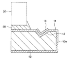
図10は、本発明の第3実施形態に係る電子装置の製造方法の要部を示す概略断面図である。なお、図10に示されている部位以外は、本実施形態の電子装置は、上記第1実施形態に示したものと同様にできる。
(Third embodiment)
FIG. 10 is a schematic cross-sectional view showing the main part of the method for manufacturing an electronic device according to the third embodiment of the present invention. Except for the part shown in FIG. 10, the electronic device of this embodiment can be the same as that shown in the first embodiment.
本実施形態は、配線基板20を、接着剤30を介してヒートシンク10の一面11上に搭載する製造方法において、上記した接着剤30におけるブリードの抑制を狙ったものである。
The present embodiment aims to suppress bleeding in the adhesive 30 described above in a manufacturing method in which the
図10に示されるように、本実施形態では、ヒートシンク10として、配線基板20が搭載される一面11のうち接着剤30が設けられる部位の周囲に、プレス加工などにより溝13を設けたものを用意する。なお、図10では、溝13の全容は示されていないが、ヒートシンク10の一面11のうち接着剤30が設けられる部位を取り囲むように形成されている。
As shown in FIG. 10, in this embodiment, the
そして、このようなヒートシンク10に対して、上記第2実施形態と同様に、ヒートシンク10の表面のうち少なくともモールド樹脂80と接する部位および一面11に、無電解Niメッキ膜10aを設ける。
For such a
続いて、本実施形態では、図10に示されるように、無電解Niメッキ膜10aの表面うち溝13内に位置する部位を、樹脂材14により被覆する。この樹脂材14としては、モールド樹脂80と密着性を有するものであればよい。
Subsequently, in the present embodiment, as shown in FIG. 10, a portion of the surface of the electroless
たとえばポリアミド系樹脂、ポリイミド系樹脂などを樹脂材14として採用し、これを塗布して硬化することにより、樹脂材14の配設がなされる。たとえばポリアミド系樹脂の場合、150℃程度で硬化させる。そして、このように樹脂材14を配設することにより、溝13内の無電解Niメッキ膜10aの表面が、樹脂材14により平滑化されたものとなる。
For example, a polyamide-based resin, a polyimide-based resin, or the like is employed as the
すなわち、ヒートシンク10の一面11のうち接着剤30が設けられる部位の周囲に位置する無電解Niメッキ膜10aの表面が、樹脂材14により、無電解Niメッキ膜10aの粗化された表面よりも平滑な表面となる。
That is, the surface of the electroless
その後は、上記第2実施形態と同様に、ヒートシンク10の一面11上に接着剤30を介して配線基板20を搭載する。そして、ワイヤボンディングやモールド樹脂80による封止を行うことで、電子装置を完成する。なお、樹脂材14は、図10に示される状態にてモールド樹脂80に封止される。
Thereafter, as in the second embodiment, the
本実施形態の製造方法によれば、ヒートシンク10の一面11において接着剤30の搭載領域の周囲では、表面が平滑化された樹脂材14が存在し、この樹脂材14では、ブリードの進展速度が極めて遅くなる。そのため、上記第2実施形態と同様に、ブリードの抑制が可能となる。
According to the manufacturing method of the present embodiment, the
また、上記製造方法によれば、ヒートシンク10の一面11のうち樹脂材14を設ける部位に、溝13を設け、無電解Niメッキ膜10aのうちこの溝13内に位置する部位を、樹脂材14により被覆している。
Further, according to the manufacturing method described above, the
それによれば、樹脂材14を溝13内に塗布することで、溝13内に樹脂が広がりやすく、樹脂材14の塗布が容易になる。また、溝13を設けることで、ブリードの進展方向に堰を形成したのと同様の状態となることから、ブリードの進展を抑制するためには、好ましい。
According to this, by applying the
ここで、本実施形態においては、溝13の形状は図示例のようなV溝に限定されるものではなく、矩形状の溝、U溝などであってもよい。また、樹脂材14は溝13の形状を継承していなくてもよく、樹脂材14により溝13が埋まっていてもよい。また、溝13は複数本設けられていてもよい。
Here, in the present embodiment, the shape of the
さらには、ヒートシンク10には溝13はないものであってもよい。その場合であっても、ヒートシンク10の一面11に位置する無電解Niメッキ膜10aの表面のうち接着剤30が設けられる部位の周囲を、モールド樹脂80と密着性を有する樹脂材14により被覆することで平滑化すればよい。
Further, the
また、本実施形態によれば、できあがった電子装置は、上記第1実施形態に示した電子装置において、配線基板20を接着剤30を介してヒートシンク10の一面11に搭載し、無電解Niメッキ膜10aは、ヒートシンク10の表面のうちモールド樹脂80と接する部位および配線基板20が搭載される部位である一面11に形成された構成を有するものとなる。
Further, according to the present embodiment, the completed electronic device is the same as the electronic device shown in the first embodiment, in which the
さらに、本実施形態の電子装置は、ヒートシンク10の一面11に位置する無電解Niメッキ膜10aの表面のうち接着剤30が設けられる部位の周囲が、モールド樹脂80と密着性を有する樹脂材14により被覆され、さらにこの樹脂材14がモールド樹脂80にて被覆された構成となる。
Furthermore, in the electronic device according to the present embodiment, the
また、溝13を設けた場合には、本実施形態の製造方法にてできあがった電子装置は、ヒートシンク10の一面11のうち樹脂材14を設けている部位に、溝13が設けられた構成を有するものとなる。
In addition, when the
(他の実施形態)
なお、上記の実施形態に示されるNi−Pメッキ膜などからなる下地メッキ膜10bは、必要に応じて設ければよいものであり、場合によっては、下地メッキ膜10bが無い構成であってもよい。
(Other embodiments)
Note that the
また、無電解Niメッキ膜10aの表面粗化状態は、上記した各図に示されるような形態に限定されるものではなく、モールド樹脂80との密着性を向上できるような凹凸形状であればよい。
In addition, the surface roughened state of the electroless
また、上記各図に示した電子装置は、一実施形態を示すものであり、電子部品が実装された配線基板を、ヒートシンクの一面上に搭載し、ヒートシンク、電子部品および配線基板をモールド樹脂により封止してなるものであれば、配線基板、電子部品、ヒートシンクなどの構成は、上記のものに限定されない。 The electronic device shown in each of the above drawings shows an embodiment. A wiring board on which electronic parts are mounted is mounted on one surface of a heat sink, and the heat sink, electronic parts, and wiring board are made of a mold resin. The configuration of the wiring board, the electronic component, the heat sink, and the like is not limited to the above as long as it is sealed.
また、上記の実施形態では、ヒートシンク10のうち配線基板20が搭載される面である一面11とは反対側の他面12を、モールド樹脂80から露出させているが、このヒートシンク10の他面12もモールド樹脂80により封止されたものであっても、本発明は適用可能である。
In the above embodiment, the
また、ヒートシンク10の一部をモールド樹脂80から露出される構成を採用する場合には、上記の実施形態のように、配線基板20が搭載される一面11とは反対側の他面12を露出する形態に限定されるものではない。
When a configuration in which a part of the
たとえば、ヒートシンク10の他面12の一部を露出させてもよいし、他面12はモールド樹脂80にて封止するようにし、ヒートシンク10における一面11と他面12の間に位置する側面を露出させてもよいし、さらには、ヒートシンク10の一面の一部を露出させてもよい。
For example, a part of the
このようにヒートシンクのどこかの一部をモールド樹脂80から露出させる場合、あるいは、すべてを封止する場合のいずれにおいても、ヒートシンク10の表面のうち少なくともモールド樹脂80と接して封止されている部位に、上記の粗化された無電解メッキ膜10aが設けられていればよい。
As described above, in a case where a part of the heat sink is exposed from the
10…ヒートシンク、10a…無電解Niメッキ膜、
10b…下地メッキ膜としてのNi−P膜、11…ヒートシンクの一面、
12…ヒートシンクの他面、13…溝、14…樹脂材、20…配線基板、
30…接着剤、40…電子部品としてのICチップ、
41…電子部品としてのコンデンサ、80…モールド樹脂。
10 ... heat sink, 10a ... electroless Ni plating film,
10b ... Ni-P film as a base plating film, 11 ... one side of heat sink,
12 ... Other surface of heat sink, 13 ... Groove, 14 ... Resin material, 20 ... Wiring board,
30 ... Adhesive, 40 ... IC chip as an electronic component,
41: Capacitor as an electronic component, 80: Mold resin.
Claims (11)
前記ヒートシンク(10)の表面のうち少なくとも前記モールド樹脂(80)と接する部位には、無電解メッキにてNiをメッキすることにより形成された無電解Niメッキ膜(10a)が形成されており、この無電解Niメッキ膜(10a)の表面は、凹凸形状を持つように粗化されていることを特徴とする電子装置。 A wiring board (20) on which electronic parts (40, 41) are mounted is mounted on one surface (11) of a heat sink (10), and the heat sink (10), the electronic parts (40, 41), and the wiring board are mounted. In an electronic device formed by sealing (20) with a mold resin (80),
An electroless Ni plating film (10a) formed by plating Ni by electroless plating is formed on at least a portion of the surface of the heat sink (10) that is in contact with the mold resin (80). An electronic device characterized in that the surface of the electroless Ni plating film (10a) is roughened so as to have an uneven shape.
前記配線基板(20)は、接着剤(30)を介して前記ヒートシンク(10)に搭載されていることを特徴とする請求項1に記載の電子装置。 The electroless Ni plating film (10a) is formed on a portion of the surface of the heat sink (10) in contact with the mold resin (80) and a portion on which the wiring board (20) is mounted,
The electronic device according to claim 1, wherein the wiring board (20) is mounted on the heat sink (10) via an adhesive (30).
前記無電解Niメッキ膜(10a)は、前記ヒートシンク(10)の表面のうち前記モールド樹脂(80)と接する部位および前記他面(12)に形成されていることを特徴とする請求項1に記載の電子装置。 The other surface (12) of the heat sink (10) is exposed from the mold resin (80),
The electroless Ni plating film (10a) is formed on a portion of the surface of the heat sink (10) that is in contact with the mold resin (80) and on the other surface (12). The electronic device described.
前記ヒートシンク(10)の表面のうち前記モールド樹脂(80)と接する部位および前記一面(11)に、無電解メッキにてNiをメッキすることにより形成され、その表面が凹凸形状を持つように粗化された無電解Niメッキ膜(10a)を設け、
前記配線基板(20)側に前記接着剤(30)を設け、前記ヒートシンク(10)を前記接着剤(30)の硬化温度以上に加熱した状態とし、
続いて、この加熱された状態にある前記ヒートシンク(10)の前記一面(11)上に前記接着剤(30)を介して前記配線基板(20)を搭載することで、前記ヒートシンク(10)の熱により、前記接着剤(30)を硬化させることを特徴とする電子装置の製造方法。 A wiring board (20) on which electronic components (40, 41) are mounted is mounted on one surface (11) of a heat sink (10) via an adhesive (30) made of a thermosetting resin, and the heat sink (10 ), In the method of manufacturing an electronic device in which the electronic component (40, 41) and the wiring board (20) are sealed with a mold resin (80),
A portion of the surface of the heat sink (10) that is in contact with the mold resin (80) and the one surface (11) are formed by plating Ni by electroless plating, and the surface is rough so as to have an uneven shape. An electroless Ni plating film (10a) is provided,
The adhesive (30) is provided on the wiring board (20) side, and the heat sink (10) is heated to a temperature equal to or higher than the curing temperature of the adhesive (30).
Subsequently, by mounting the wiring board (20) on the one surface (11) of the heat sink (10) in the heated state via the adhesive (30), the heat sink (10) A method of manufacturing an electronic device, wherein the adhesive (30) is cured by heat.
前記ヒートシンク(10)の表面のうち前記モールド樹脂(80)と接する部位および前記一面(11)に、無電解メッキにてNiをメッキすることにより形成され、その表面が凹凸形状を持つように粗化された無電解Niメッキ膜(10a)を設け、
続いて、前記ヒートシンク(10)の前記一面(11)に位置する前記無電解Niメッキ膜(10a)の表面のうち前記接着剤(30)が設けられる部位の周囲を、前記モールド樹脂(80)と密着性を有する樹脂材(14)により被覆することで平滑化した後、
前記ヒートシンク(10)の前記一面(11)上に前記接着剤(30)を介して前記配線基板(20)を搭載することを特徴とする電子装置の製造方法。 A wiring board (20) on which electronic components (40, 41) are mounted is mounted on one surface (11) of a heat sink (10) via an adhesive (30), and the heat sink (10), the electronic component ( 40, 41) and the method of manufacturing an electronic device in which the wiring board (20) is sealed with a mold resin (80).
A portion of the surface of the heat sink (10) that is in contact with the mold resin (80) and the one surface (11) are formed by plating Ni by electroless plating, and the surface is rough so as to have an uneven shape. An electroless Ni plating film (10a) is provided,
Subsequently, around the portion where the adhesive (30) is provided on the surface of the electroless Ni plating film (10a) located on the one surface (11) of the heat sink (10), the mold resin (80) And smoothing by covering with an adhesive resin material (14),
A method of manufacturing an electronic device, comprising mounting the wiring board (20) on the one surface (11) of the heat sink (10) via the adhesive (30).
前記ヒートシンク(10)の表面のうち前記モールド樹脂(80)と接する部位および前記一面(11)に、前記無電解Niメッキ膜(10a)を設け、
続いて、前記無電解Niメッキ膜(10a)の表面のうち前記溝(13)内に位置する部位を、前記樹脂材(14)により被覆することを特徴とする電子装置の製造方法。 After providing the groove (13) in the part of the one surface (11) of the heat sink (10) where the resin material (14) is provided,
The electroless Ni plating film (10a) is provided on the surface of the heat sink (10) in contact with the mold resin (80) and the one surface (11),
Then, the part located in the said groove | channel (13) among the surfaces of the said electroless Ni plating film (10a) is coat | covered with the said resin material (14), The manufacturing method of the electronic device characterized by the above-mentioned.
Priority Applications (1)
| Application Number | Priority Date | Filing Date | Title |
|---|---|---|---|
| JP2006015925A JP4591362B2 (en) | 2006-01-25 | 2006-01-25 | Manufacturing method of electronic device |
Applications Claiming Priority (1)
| Application Number | Priority Date | Filing Date | Title |
|---|---|---|---|
| JP2006015925A JP4591362B2 (en) | 2006-01-25 | 2006-01-25 | Manufacturing method of electronic device |
Publications (2)
| Publication Number | Publication Date |
|---|---|
| JP2007201036A true JP2007201036A (en) | 2007-08-09 |
| JP4591362B2 JP4591362B2 (en) | 2010-12-01 |
Family
ID=38455339
Family Applications (1)
| Application Number | Title | Priority Date | Filing Date |
|---|---|---|---|
| JP2006015925A Expired - Fee Related JP4591362B2 (en) | 2006-01-25 | 2006-01-25 | Manufacturing method of electronic device |
Country Status (1)
| Country | Link |
|---|---|
| JP (1) | JP4591362B2 (en) |
Cited By (4)
| Publication number | Priority date | Publication date | Assignee | Title |
|---|---|---|---|---|
| JP2011059571A (en) * | 2009-09-14 | 2011-03-24 | Sumitomo Electric Ind Ltd | Optical sub-assembly |
| JP2016115806A (en) * | 2014-12-15 | 2016-06-23 | トヨタ自動車株式会社 | Semiconductor device |
| EP2261933A4 (en) * | 2008-04-08 | 2018-03-28 | Murata Manufacturing Co. Ltd. | Capacitor and method for manufacturing the same |
| JP2018163962A (en) * | 2017-03-24 | 2018-10-18 | 株式会社東芝 | Semiconductor device and method of manufacturing the same |
Citations (3)
| Publication number | Priority date | Publication date | Assignee | Title |
|---|---|---|---|---|
| JP2003060137A (en) * | 2001-08-08 | 2003-02-28 | Ibiden Co Ltd | Substrate for module |
| JP2004349497A (en) * | 2003-05-22 | 2004-12-09 | Shinko Electric Ind Co Ltd | Packaging component and semiconductor package |
| JP2005328018A (en) * | 2004-04-14 | 2005-11-24 | Denso Corp | Semiconductor device |
-
2006
- 2006-01-25 JP JP2006015925A patent/JP4591362B2/en not_active Expired - Fee Related
Patent Citations (3)
| Publication number | Priority date | Publication date | Assignee | Title |
|---|---|---|---|---|
| JP2003060137A (en) * | 2001-08-08 | 2003-02-28 | Ibiden Co Ltd | Substrate for module |
| JP2004349497A (en) * | 2003-05-22 | 2004-12-09 | Shinko Electric Ind Co Ltd | Packaging component and semiconductor package |
| JP2005328018A (en) * | 2004-04-14 | 2005-11-24 | Denso Corp | Semiconductor device |
Cited By (4)
| Publication number | Priority date | Publication date | Assignee | Title |
|---|---|---|---|---|
| EP2261933A4 (en) * | 2008-04-08 | 2018-03-28 | Murata Manufacturing Co. Ltd. | Capacitor and method for manufacturing the same |
| JP2011059571A (en) * | 2009-09-14 | 2011-03-24 | Sumitomo Electric Ind Ltd | Optical sub-assembly |
| JP2016115806A (en) * | 2014-12-15 | 2016-06-23 | トヨタ自動車株式会社 | Semiconductor device |
| JP2018163962A (en) * | 2017-03-24 | 2018-10-18 | 株式会社東芝 | Semiconductor device and method of manufacturing the same |
Also Published As
| Publication number | Publication date |
|---|---|
| JP4591362B2 (en) | 2010-12-01 |
Similar Documents
| Publication | Publication Date | Title |
|---|---|---|
| JP5387685B2 (en) | Manufacturing method of semiconductor device | |
| JP2008172172A (en) | Electronic controller and method of manufacturing the same | |
| JP2006100752A (en) | Circuit arrangement and its manufacturing method | |
| JP4967701B2 (en) | Power semiconductor device | |
| JPH0883861A (en) | Metal foil material for coating semiconductor package and semiconductor device | |
| JP5126201B2 (en) | Semiconductor module and manufacturing method thereof | |
| JP2006253354A (en) | Circuit device and its manufacturing method | |
| JP5262983B2 (en) | Mold package and manufacturing method thereof | |
| JP4591362B2 (en) | Manufacturing method of electronic device | |
| JP2009267344A (en) | Method of manufacturing semiconductor device | |
| JP3606078B2 (en) | Semiconductor device and manufacturing method thereof | |
| JP2000236060A (en) | Semiconductor device | |
| JP2006191143A (en) | Semiconductor device | |
| JP5035356B2 (en) | Resin-sealed electronic device and method for manufacturing the same | |
| JP5083076B2 (en) | Manufacturing method of electronic device | |
| JP2008211168A (en) | Semiconductor device and semiconductor module | |
| JP2010141158A (en) | Electronic device | |
| JP2015106649A (en) | Electronic device | |
| JP2008258435A (en) | Semiconductor device, and manufacturing method thereof | |
| CN209880589U (en) | Semiconductor packaging structure | |
| JP2010199516A (en) | Electronic device | |
| TWM545363U (en) | Chip package structure | |
| JP2008147267A (en) | Semiconductor device and manufacturing method therefor, and lead frame with radiation board | |
| JP2008288566A (en) | Semiconductor device | |
| JP3277830B2 (en) | How to assemble electronic components |
Legal Events
| Date | Code | Title | Description |
|---|---|---|---|
| A621 | Written request for application examination |
Free format text: JAPANESE INTERMEDIATE CODE: A621 Effective date: 20080204 |
|
| A977 | Report on retrieval |
Free format text: JAPANESE INTERMEDIATE CODE: A971007 Effective date: 20100125 |
|
| A131 | Notification of reasons for refusal |
Free format text: JAPANESE INTERMEDIATE CODE: A131 Effective date: 20100209 |
|
| A521 | Request for written amendment filed |
Free format text: JAPANESE INTERMEDIATE CODE: A523 Effective date: 20100329 |
|
| A131 | Notification of reasons for refusal |
Free format text: JAPANESE INTERMEDIATE CODE: A131 Effective date: 20100518 |
|
| A521 | Request for written amendment filed |
Free format text: JAPANESE INTERMEDIATE CODE: A523 Effective date: 20100709 |
|
| TRDD | Decision of grant or rejection written | ||
| A01 | Written decision to grant a patent or to grant a registration (utility model) |
Free format text: JAPANESE INTERMEDIATE CODE: A01 Effective date: 20100817 |
|
| A01 | Written decision to grant a patent or to grant a registration (utility model) |
Free format text: JAPANESE INTERMEDIATE CODE: A01 |
|
| A61 | First payment of annual fees (during grant procedure) |
Free format text: JAPANESE INTERMEDIATE CODE: A61 Effective date: 20100830 |
|
| FPAY | Renewal fee payment (event date is renewal date of database) |
Free format text: PAYMENT UNTIL: 20130924 Year of fee payment: 3 |
|
| R151 | Written notification of patent or utility model registration |
Ref document number: 4591362 Country of ref document: JP Free format text: JAPANESE INTERMEDIATE CODE: R151 |
|
| FPAY | Renewal fee payment (event date is renewal date of database) |
Free format text: PAYMENT UNTIL: 20130924 Year of fee payment: 3 |
|
| R250 | Receipt of annual fees |
Free format text: JAPANESE INTERMEDIATE CODE: R250 |
|
| R250 | Receipt of annual fees |
Free format text: JAPANESE INTERMEDIATE CODE: R250 |
|
| R250 | Receipt of annual fees |
Free format text: JAPANESE INTERMEDIATE CODE: R250 |
|
| R250 | Receipt of annual fees |
Free format text: JAPANESE INTERMEDIATE CODE: R250 |
|
| R250 | Receipt of annual fees |
Free format text: JAPANESE INTERMEDIATE CODE: R250 |
|
| LAPS | Cancellation because of no payment of annual fees |