JP2006120943A - チップ内蔵基板及びその製造方法 - Google Patents
チップ内蔵基板及びその製造方法 Download PDFInfo
- Publication number
- JP2006120943A JP2006120943A JP2004308558A JP2004308558A JP2006120943A JP 2006120943 A JP2006120943 A JP 2006120943A JP 2004308558 A JP2004308558 A JP 2004308558A JP 2004308558 A JP2004308558 A JP 2004308558A JP 2006120943 A JP2006120943 A JP 2006120943A
- Authority
- JP
- Japan
- Prior art keywords
- base material
- resin base
- chip
- substrate
- resin
- Prior art date
- Legal status (The legal status is an assumption and is not a legal conclusion. Google has not performed a legal analysis and makes no representation as to the accuracy of the status listed.)
- Pending
Links
Images


Classifications
-
- H—ELECTRICITY
- H01—ELECTRIC ELEMENTS
- H01L—SEMICONDUCTOR DEVICES NOT COVERED BY CLASS H10
- H01L23/00—Details of semiconductor or other solid state devices
- H01L23/28—Encapsulations, e.g. encapsulating layers, coatings, e.g. for protection
- H01L23/29—Encapsulations, e.g. encapsulating layers, coatings, e.g. for protection characterised by the material, e.g. carbon
- H01L23/293—Organic, e.g. plastic
-
- H—ELECTRICITY
- H01—ELECTRIC ELEMENTS
- H01L—SEMICONDUCTOR DEVICES NOT COVERED BY CLASS H10
- H01L21/00—Processes or apparatus adapted for the manufacture or treatment of semiconductor or solid state devices or of parts thereof
- H01L21/02—Manufacture or treatment of semiconductor devices or of parts thereof
- H01L21/04—Manufacture or treatment of semiconductor devices or of parts thereof the devices having at least one potential-jump barrier or surface barrier, e.g. PN junction, depletion layer or carrier concentration layer
- H01L21/50—Assembly of semiconductor devices using processes or apparatus not provided for in a single one of the subgroups H01L21/06 - H01L21/326, e.g. sealing of a cap to a base of a container
- H01L21/56—Encapsulations, e.g. encapsulation layers, coatings
- H01L21/568—Temporary substrate used as encapsulation process aid
-
- H—ELECTRICITY
- H01—ELECTRIC ELEMENTS
- H01L—SEMICONDUCTOR DEVICES NOT COVERED BY CLASS H10
- H01L23/00—Details of semiconductor or other solid state devices
- H01L23/28—Encapsulations, e.g. encapsulating layers, coatings, e.g. for protection
- H01L23/29—Encapsulations, e.g. encapsulating layers, coatings, e.g. for protection characterised by the material, e.g. carbon
-
- H—ELECTRICITY
- H01—ELECTRIC ELEMENTS
- H01L—SEMICONDUCTOR DEVICES NOT COVERED BY CLASS H10
- H01L23/00—Details of semiconductor or other solid state devices
- H01L23/28—Encapsulations, e.g. encapsulating layers, coatings, e.g. for protection
- H01L23/31—Encapsulations, e.g. encapsulating layers, coatings, e.g. for protection characterised by the arrangement or shape
- H01L23/3107—Encapsulations, e.g. encapsulating layers, coatings, e.g. for protection characterised by the arrangement or shape the device being completely enclosed
- H01L23/3121—Encapsulations, e.g. encapsulating layers, coatings, e.g. for protection characterised by the arrangement or shape the device being completely enclosed a substrate forming part of the encapsulation
- H01L23/3128—Encapsulations, e.g. encapsulating layers, coatings, e.g. for protection characterised by the arrangement or shape the device being completely enclosed a substrate forming part of the encapsulation the substrate having spherical bumps for external connection
-
- H—ELECTRICITY
- H01—ELECTRIC ELEMENTS
- H01L—SEMICONDUCTOR DEVICES NOT COVERED BY CLASS H10
- H01L23/00—Details of semiconductor or other solid state devices
- H01L23/52—Arrangements for conducting electric current within the device in operation from one component to another, i.e. interconnections, e.g. wires, lead frames
- H01L23/538—Arrangements for conducting electric current within the device in operation from one component to another, i.e. interconnections, e.g. wires, lead frames the interconnection structure between a plurality of semiconductor chips being formed on, or in, insulating substrates
- H01L23/5389—Arrangements for conducting electric current within the device in operation from one component to another, i.e. interconnections, e.g. wires, lead frames the interconnection structure between a plurality of semiconductor chips being formed on, or in, insulating substrates the chips being integrally enclosed by the interconnect and support structures
-
- H—ELECTRICITY
- H01—ELECTRIC ELEMENTS
- H01L—SEMICONDUCTOR DEVICES NOT COVERED BY CLASS H10
- H01L24/00—Arrangements for connecting or disconnecting semiconductor or solid-state bodies; Methods or apparatus related thereto
- H01L24/01—Means for bonding being attached to, or being formed on, the surface to be connected, e.g. chip-to-package, die-attach, "first-level" interconnects; Manufacturing methods related thereto
- H01L24/18—High density interconnect [HDI] connectors; Manufacturing methods related thereto
- H01L24/19—Manufacturing methods of high density interconnect preforms
-
- H—ELECTRICITY
- H01—ELECTRIC ELEMENTS
- H01L—SEMICONDUCTOR DEVICES NOT COVERED BY CLASS H10
- H01L24/00—Arrangements for connecting or disconnecting semiconductor or solid-state bodies; Methods or apparatus related thereto
- H01L24/01—Means for bonding being attached to, or being formed on, the surface to be connected, e.g. chip-to-package, die-attach, "first-level" interconnects; Manufacturing methods related thereto
- H01L24/18—High density interconnect [HDI] connectors; Manufacturing methods related thereto
- H01L24/20—Structure, shape, material or disposition of high density interconnect preforms
-
- H—ELECTRICITY
- H01—ELECTRIC ELEMENTS
- H01L—SEMICONDUCTOR DEVICES NOT COVERED BY CLASS H10
- H01L24/00—Arrangements for connecting or disconnecting semiconductor or solid-state bodies; Methods or apparatus related thereto
- H01L24/01—Means for bonding being attached to, or being formed on, the surface to be connected, e.g. chip-to-package, die-attach, "first-level" interconnects; Manufacturing methods related thereto
- H01L24/18—High density interconnect [HDI] connectors; Manufacturing methods related thereto
- H01L24/23—Structure, shape, material or disposition of the high density interconnect connectors after the connecting process
- H01L24/24—Structure, shape, material or disposition of the high density interconnect connectors after the connecting process of an individual high density interconnect connector
-
- H—ELECTRICITY
- H01—ELECTRIC ELEMENTS
- H01L—SEMICONDUCTOR DEVICES NOT COVERED BY CLASS H10
- H01L24/00—Arrangements for connecting or disconnecting semiconductor or solid-state bodies; Methods or apparatus related thereto
- H01L24/80—Methods for connecting semiconductor or other solid state bodies using means for bonding being attached to, or being formed on, the surface to be connected
- H01L24/82—Methods for connecting semiconductor or other solid state bodies using means for bonding being attached to, or being formed on, the surface to be connected by forming build-up interconnects at chip-level, e.g. for high density interconnects [HDI]
-
- H—ELECTRICITY
- H01—ELECTRIC ELEMENTS
- H01L—SEMICONDUCTOR DEVICES NOT COVERED BY CLASS H10
- H01L2224/00—Indexing scheme for arrangements for connecting or disconnecting semiconductor or solid-state bodies and methods related thereto as covered by H01L24/00
- H01L2224/01—Means for bonding being attached to, or being formed on, the surface to be connected, e.g. chip-to-package, die-attach, "first-level" interconnects; Manufacturing methods related thereto
- H01L2224/02—Bonding areas; Manufacturing methods related thereto
- H01L2224/04—Structure, shape, material or disposition of the bonding areas prior to the connecting process
- H01L2224/04105—Bonding areas formed on an encapsulation of the semiconductor or solid-state body, e.g. bonding areas on chip-scale packages
-
- H—ELECTRICITY
- H01—ELECTRIC ELEMENTS
- H01L—SEMICONDUCTOR DEVICES NOT COVERED BY CLASS H10
- H01L2224/00—Indexing scheme for arrangements for connecting or disconnecting semiconductor or solid-state bodies and methods related thereto as covered by H01L24/00
- H01L2224/01—Means for bonding being attached to, or being formed on, the surface to be connected, e.g. chip-to-package, die-attach, "first-level" interconnects; Manufacturing methods related thereto
- H01L2224/10—Bump connectors; Manufacturing methods related thereto
- H01L2224/12—Structure, shape, material or disposition of the bump connectors prior to the connecting process
- H01L2224/12105—Bump connectors formed on an encapsulation of the semiconductor or solid-state body, e.g. bumps on chip-scale packages
-
- H—ELECTRICITY
- H01—ELECTRIC ELEMENTS
- H01L—SEMICONDUCTOR DEVICES NOT COVERED BY CLASS H10
- H01L2224/00—Indexing scheme for arrangements for connecting or disconnecting semiconductor or solid-state bodies and methods related thereto as covered by H01L24/00
- H01L2224/01—Means for bonding being attached to, or being formed on, the surface to be connected, e.g. chip-to-package, die-attach, "first-level" interconnects; Manufacturing methods related thereto
- H01L2224/18—High density interconnect [HDI] connectors; Manufacturing methods related thereto
- H01L2224/20—Structure, shape, material or disposition of high density interconnect preforms
- H01L2224/21—Structure, shape, material or disposition of high density interconnect preforms of an individual HDI interconnect
- H01L2224/211—Disposition
-
- H—ELECTRICITY
- H01—ELECTRIC ELEMENTS
- H01L—SEMICONDUCTOR DEVICES NOT COVERED BY CLASS H10
- H01L2224/00—Indexing scheme for arrangements for connecting or disconnecting semiconductor or solid-state bodies and methods related thereto as covered by H01L24/00
- H01L2224/01—Means for bonding being attached to, or being formed on, the surface to be connected, e.g. chip-to-package, die-attach, "first-level" interconnects; Manufacturing methods related thereto
- H01L2224/18—High density interconnect [HDI] connectors; Manufacturing methods related thereto
- H01L2224/23—Structure, shape, material or disposition of the high density interconnect connectors after the connecting process
- H01L2224/24—Structure, shape, material or disposition of the high density interconnect connectors after the connecting process of an individual high density interconnect connector
- H01L2224/241—Disposition
- H01L2224/24151—Connecting between a semiconductor or solid-state body and an item not being a semiconductor or solid-state body, e.g. chip-to-substrate, chip-to-passive
- H01L2224/24221—Connecting between a semiconductor or solid-state body and an item not being a semiconductor or solid-state body, e.g. chip-to-substrate, chip-to-passive the body and the item being stacked
- H01L2224/24225—Connecting between a semiconductor or solid-state body and an item not being a semiconductor or solid-state body, e.g. chip-to-substrate, chip-to-passive the body and the item being stacked the item being non-metallic, e.g. insulating substrate with or without metallisation
- H01L2224/24226—Connecting between a semiconductor or solid-state body and an item not being a semiconductor or solid-state body, e.g. chip-to-substrate, chip-to-passive the body and the item being stacked the item being non-metallic, e.g. insulating substrate with or without metallisation the HDI interconnect connecting to the same level of the item at which the semiconductor or solid-state body is mounted, e.g. the item being planar
-
- H—ELECTRICITY
- H01—ELECTRIC ELEMENTS
- H01L—SEMICONDUCTOR DEVICES NOT COVERED BY CLASS H10
- H01L2224/00—Indexing scheme for arrangements for connecting or disconnecting semiconductor or solid-state bodies and methods related thereto as covered by H01L24/00
- H01L2224/01—Means for bonding being attached to, or being formed on, the surface to be connected, e.g. chip-to-package, die-attach, "first-level" interconnects; Manufacturing methods related thereto
- H01L2224/26—Layer connectors, e.g. plate connectors, solder or adhesive layers; Manufacturing methods related thereto
- H01L2224/31—Structure, shape, material or disposition of the layer connectors after the connecting process
- H01L2224/32—Structure, shape, material or disposition of the layer connectors after the connecting process of an individual layer connector
- H01L2224/321—Disposition
- H01L2224/32151—Disposition the layer connector connecting between a semiconductor or solid-state body and an item not being a semiconductor or solid-state body, e.g. chip-to-substrate, chip-to-passive
- H01L2224/32221—Disposition the layer connector connecting between a semiconductor or solid-state body and an item not being a semiconductor or solid-state body, e.g. chip-to-substrate, chip-to-passive the body and the item being stacked
- H01L2224/32225—Disposition the layer connector connecting between a semiconductor or solid-state body and an item not being a semiconductor or solid-state body, e.g. chip-to-substrate, chip-to-passive the body and the item being stacked the item being non-metallic, e.g. insulating substrate with or without metallisation
-
- H—ELECTRICITY
- H01—ELECTRIC ELEMENTS
- H01L—SEMICONDUCTOR DEVICES NOT COVERED BY CLASS H10
- H01L2224/00—Indexing scheme for arrangements for connecting or disconnecting semiconductor or solid-state bodies and methods related thereto as covered by H01L24/00
- H01L2224/73—Means for bonding being of different types provided for in two or more of groups H01L2224/10, H01L2224/18, H01L2224/26, H01L2224/34, H01L2224/42, H01L2224/50, H01L2224/63, H01L2224/71
- H01L2224/732—Location after the connecting process
- H01L2224/73251—Location after the connecting process on different surfaces
- H01L2224/73267—Layer and HDI connectors
-
- H—ELECTRICITY
- H01—ELECTRIC ELEMENTS
- H01L—SEMICONDUCTOR DEVICES NOT COVERED BY CLASS H10
- H01L2224/00—Indexing scheme for arrangements for connecting or disconnecting semiconductor or solid-state bodies and methods related thereto as covered by H01L24/00
- H01L2224/80—Methods for connecting semiconductor or other solid state bodies using means for bonding being attached to, or being formed on, the surface to be connected
- H01L2224/82—Methods for connecting semiconductor or other solid state bodies using means for bonding being attached to, or being formed on, the surface to be connected by forming build-up interconnects at chip-level, e.g. for high density interconnects [HDI]
- H01L2224/82001—Methods for connecting semiconductor or other solid state bodies using means for bonding being attached to, or being formed on, the surface to be connected by forming build-up interconnects at chip-level, e.g. for high density interconnects [HDI] involving a temporary auxiliary member not forming part of the bonding apparatus
-
- H—ELECTRICITY
- H01—ELECTRIC ELEMENTS
- H01L—SEMICONDUCTOR DEVICES NOT COVERED BY CLASS H10
- H01L2224/00—Indexing scheme for arrangements for connecting or disconnecting semiconductor or solid-state bodies and methods related thereto as covered by H01L24/00
- H01L2224/80—Methods for connecting semiconductor or other solid state bodies using means for bonding being attached to, or being formed on, the surface to be connected
- H01L2224/83—Methods for connecting semiconductor or other solid state bodies using means for bonding being attached to, or being formed on, the surface to be connected using a layer connector
- H01L2224/8319—Arrangement of the layer connectors prior to mounting
- H01L2224/83191—Arrangement of the layer connectors prior to mounting wherein the layer connectors are disposed only on the semiconductor or solid-state body
-
- H—ELECTRICITY
- H01—ELECTRIC ELEMENTS
- H01L—SEMICONDUCTOR DEVICES NOT COVERED BY CLASS H10
- H01L2224/00—Indexing scheme for arrangements for connecting or disconnecting semiconductor or solid-state bodies and methods related thereto as covered by H01L24/00
- H01L2224/91—Methods for connecting semiconductor or solid state bodies including different methods provided for in two or more of groups H01L2224/80 - H01L2224/90
- H01L2224/92—Specific sequence of method steps
- H01L2224/922—Connecting different surfaces of the semiconductor or solid-state body with connectors of different types
- H01L2224/9222—Sequential connecting processes
- H01L2224/92242—Sequential connecting processes the first connecting process involving a layer connector
- H01L2224/92244—Sequential connecting processes the first connecting process involving a layer connector the second connecting process involving a build-up interconnect
-
- H—ELECTRICITY
- H01—ELECTRIC ELEMENTS
- H01L—SEMICONDUCTOR DEVICES NOT COVERED BY CLASS H10
- H01L2924/00—Indexing scheme for arrangements or methods for connecting or disconnecting semiconductor or solid-state bodies as covered by H01L24/00
- H01L2924/01—Chemical elements
- H01L2924/01006—Carbon [C]
-
- H—ELECTRICITY
- H01—ELECTRIC ELEMENTS
- H01L—SEMICONDUCTOR DEVICES NOT COVERED BY CLASS H10
- H01L2924/00—Indexing scheme for arrangements or methods for connecting or disconnecting semiconductor or solid-state bodies as covered by H01L24/00
- H01L2924/01—Chemical elements
- H01L2924/01013—Aluminum [Al]
-
- H—ELECTRICITY
- H01—ELECTRIC ELEMENTS
- H01L—SEMICONDUCTOR DEVICES NOT COVERED BY CLASS H10
- H01L2924/00—Indexing scheme for arrangements or methods for connecting or disconnecting semiconductor or solid-state bodies as covered by H01L24/00
- H01L2924/01—Chemical elements
- H01L2924/01029—Copper [Cu]
-
- H—ELECTRICITY
- H01—ELECTRIC ELEMENTS
- H01L—SEMICONDUCTOR DEVICES NOT COVERED BY CLASS H10
- H01L2924/00—Indexing scheme for arrangements or methods for connecting or disconnecting semiconductor or solid-state bodies as covered by H01L24/00
- H01L2924/01—Chemical elements
- H01L2924/0103—Zinc [Zn]
-
- H—ELECTRICITY
- H01—ELECTRIC ELEMENTS
- H01L—SEMICONDUCTOR DEVICES NOT COVERED BY CLASS H10
- H01L2924/00—Indexing scheme for arrangements or methods for connecting or disconnecting semiconductor or solid-state bodies as covered by H01L24/00
- H01L2924/01—Chemical elements
- H01L2924/01033—Arsenic [As]
-
- H—ELECTRICITY
- H01—ELECTRIC ELEMENTS
- H01L—SEMICONDUCTOR DEVICES NOT COVERED BY CLASS H10
- H01L2924/00—Indexing scheme for arrangements or methods for connecting or disconnecting semiconductor or solid-state bodies as covered by H01L24/00
- H01L2924/01—Chemical elements
- H01L2924/01075—Rhenium [Re]
-
- H—ELECTRICITY
- H01—ELECTRIC ELEMENTS
- H01L—SEMICONDUCTOR DEVICES NOT COVERED BY CLASS H10
- H01L2924/00—Indexing scheme for arrangements or methods for connecting or disconnecting semiconductor or solid-state bodies as covered by H01L24/00
- H01L2924/01—Chemical elements
- H01L2924/01078—Platinum [Pt]
-
- H—ELECTRICITY
- H01—ELECTRIC ELEMENTS
- H01L—SEMICONDUCTOR DEVICES NOT COVERED BY CLASS H10
- H01L2924/00—Indexing scheme for arrangements or methods for connecting or disconnecting semiconductor or solid-state bodies as covered by H01L24/00
- H01L2924/01—Chemical elements
- H01L2924/01079—Gold [Au]
-
- H—ELECTRICITY
- H01—ELECTRIC ELEMENTS
- H01L—SEMICONDUCTOR DEVICES NOT COVERED BY CLASS H10
- H01L2924/00—Indexing scheme for arrangements or methods for connecting or disconnecting semiconductor or solid-state bodies as covered by H01L24/00
- H01L2924/10—Details of semiconductor or other solid state devices to be connected
- H01L2924/11—Device type
- H01L2924/12—Passive devices, e.g. 2 terminal devices
- H01L2924/1204—Optical Diode
- H01L2924/12042—LASER
-
- H—ELECTRICITY
- H01—ELECTRIC ELEMENTS
- H01L—SEMICONDUCTOR DEVICES NOT COVERED BY CLASS H10
- H01L2924/00—Indexing scheme for arrangements or methods for connecting or disconnecting semiconductor or solid-state bodies as covered by H01L24/00
- H01L2924/15—Details of package parts other than the semiconductor or other solid state devices to be connected
- H01L2924/151—Die mounting substrate
- H01L2924/153—Connection portion
- H01L2924/1531—Connection portion the connection portion being formed only on the surface of the substrate opposite to the die mounting surface
- H01L2924/15311—Connection portion the connection portion being formed only on the surface of the substrate opposite to the die mounting surface being a ball array, e.g. BGA
-
- H—ELECTRICITY
- H01—ELECTRIC ELEMENTS
- H01L—SEMICONDUCTOR DEVICES NOT COVERED BY CLASS H10
- H01L2924/00—Indexing scheme for arrangements or methods for connecting or disconnecting semiconductor or solid-state bodies as covered by H01L24/00
- H01L2924/15—Details of package parts other than the semiconductor or other solid state devices to be connected
- H01L2924/181—Encapsulation
- H01L2924/1815—Shape
- H01L2924/1816—Exposing the passive side of the semiconductor or solid-state body
- H01L2924/18162—Exposing the passive side of the semiconductor or solid-state body of a chip with build-up interconnect
-
- H—ELECTRICITY
- H01—ELECTRIC ELEMENTS
- H01L—SEMICONDUCTOR DEVICES NOT COVERED BY CLASS H10
- H01L2924/00—Indexing scheme for arrangements or methods for connecting or disconnecting semiconductor or solid-state bodies as covered by H01L24/00
- H01L2924/30—Technical effects
- H01L2924/35—Mechanical effects
- H01L2924/351—Thermal stress
- H01L2924/3511—Warping
Abstract
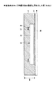
【解決手段】 樹脂に球状のフィラーを樹脂基材31全体に対して60〜90wt%含有させた樹脂基材31により半導体チップ33を内蔵すると共に、樹脂基材31を貫通する貫通ビア44と、樹脂基材31の上面31aに形成され、貫通ビア44と電気的に接続された第1の外部接続端子53と、樹脂基材31の下面31bに形成され、貫通ビア44と電気的に接続された第2の外部接続端子54とを設けた構成とした。
【選択図】 図2
Description
(実施例)
始めに、図2を参照して、本発明の実施例によるチップ内蔵基板30について説明する。図2は、本発明の実施例によるチップ内蔵基板の断面図である。チップ内蔵基板30は、大略すると半導体チップ33と、樹脂基材31と、ビア41と、貫通ビア44と、配線46と、ソルダーレジスト48,61と、Ni/Au層50,55と、第1の外部接続端子53と、第2の外部接続端子54と、はんだボール59とを有した構成とされている。
11,66 支持板
11a,31a 上面
11b,31b 下面
12,65 接着剤
13,33 半導体チップ
14,34 半導体チップ本体
15,37 電極パッド
17,31 樹脂基材
17a 面
18,41 ビア
19,46 配線
20 外部接続端子
21,48,68 ソルダーレジスト
22,59 はんだボール
23 樹脂層
25,100 他のチップ内蔵基板
38 Ni層
42 Cu膜
43 シード層
44 貫通ビア
46A,53A 領域
49,58,71,75,78 開口部
50,55 Ni/Au層
51,56 Ni層
52,57 Au層
53 第1の外部接続端子
54 第2の外部接続端子
67 銅箔
72 貫通孔
74,77,81 ドライフィルムレジスト
M1 厚さ
Claims (7)
- 半導体チップと、
該半導体チップを内蔵する樹脂基材と、
外部接続端子とを有するチップ内蔵基板において、
前記樹脂基材は、樹脂からなり、該樹脂に球状のフィラーを前記樹脂基材全体に対して60〜90wt%含有させたことを特徴とするチップ内蔵基板。 - 前記樹脂基材は、ガラス転移温度付近の温度での弾性率が1GPa〜3GPaであることを特徴とする請求項1に記載のチップ内蔵基板。
- 前記樹脂基材は、ガラス転移温度よりも低い温度での熱膨張係数が10ppm〜15ppmであることを特徴とする請求項1または2に記載のチップ内蔵基板。
- 前記樹脂基材の両面に前記外部接続端子を設けたことを特徴とする請求項1乃至3のいずれか1項に記載のチップ内蔵基板。
- 前記半導体チップは、前記外部接続端子と接続される電極パッドを有し、
該電極パッドの材料にAlを用いた際、前記電極パッドをジンケート処理し、前記電極パッド上にNi層を設けたことを特徴とする請求項1乃至4のいずれか1項に記載のチップ内蔵基板。 - 半導体チップと、
該半導体チップを内蔵する樹脂基材と、
外部接続端子とを有するチップ内蔵基板の製造方法において、
支持板上に前記半導体チップを配設する半導体チップ配設工程と、
前記半導体チップを覆うよう前記支持板上に前記樹脂基材を配設する樹脂基材配設工程と、
前記支持板を除去する支持板除去工程とを備え、
前記樹脂基材には、樹脂からなり、該樹脂に球状のフィラーを前記樹脂基材全体に対して60〜90wt%含有させることを特徴とするチップ内蔵基板の製造方法。 - 前記樹脂基材を貫通する貫通ビアを形成する貫通ビア形成工程と、
前記樹脂基材の一方の面に、前記貫通ビアと電気的に接続される第1の外部接続端子を形成する第1の外部接続端子形成工程と、
前記樹脂基材の他方の面に、前記貫通ビアと電気的に接続される第2の外部接続端子を形成する第2の外部接続端子形成工程とを設けたことを特徴とする請求項6に記載のチップ内蔵基板の製造方法。
Priority Applications (6)
| Application Number | Priority Date | Filing Date | Title |
|---|---|---|---|
| JP2004308558A JP2006120943A (ja) | 2004-10-22 | 2004-10-22 | チップ内蔵基板及びその製造方法 |
| EP05255576A EP1650798A3 (en) | 2004-10-22 | 2005-09-12 | A substrate having a built-in chip and external connection terminals on both sides and a method for manufacturing the same |
| TW094131451A TW200614900A (en) | 2004-10-22 | 2005-09-13 | A substrate having a built-in chip and external connection terminals on both sides and a method for manufacturing the same |
| US11/224,821 US7312536B2 (en) | 2004-10-22 | 2005-09-13 | Substrate having a built-in chip and external connection terminals on both sides and a method for manufacturing the same |
| KR1020050087299A KR20060051422A (ko) | 2004-10-22 | 2005-09-20 | 내장 칩을 갖고 그 양측에 외부 접속 단자를 갖는 기판과그 제조 방법 |
| CNB2005101315584A CN100446225C (zh) | 2004-10-22 | 2005-09-21 | 具有内装芯片和两侧上的外部连接端子的基板及其制造方法 |
Applications Claiming Priority (1)
| Application Number | Priority Date | Filing Date | Title |
|---|---|---|---|
| JP2004308558A JP2006120943A (ja) | 2004-10-22 | 2004-10-22 | チップ内蔵基板及びその製造方法 |
Publications (2)
| Publication Number | Publication Date |
|---|---|
| JP2006120943A true JP2006120943A (ja) | 2006-05-11 |
| JP2006120943A5 JP2006120943A5 (ja) | 2007-11-01 |
Family
ID=35615238
Family Applications (1)
| Application Number | Title | Priority Date | Filing Date |
|---|---|---|---|
| JP2004308558A Pending JP2006120943A (ja) | 2004-10-22 | 2004-10-22 | チップ内蔵基板及びその製造方法 |
Country Status (6)
| Country | Link |
|---|---|
| US (1) | US7312536B2 (ja) |
| EP (1) | EP1650798A3 (ja) |
| JP (1) | JP2006120943A (ja) |
| KR (1) | KR20060051422A (ja) |
| CN (1) | CN100446225C (ja) |
| TW (1) | TW200614900A (ja) |
Cited By (6)
| Publication number | Priority date | Publication date | Assignee | Title |
|---|---|---|---|---|
| JP2008166816A (ja) * | 2006-12-30 | 2008-07-17 | Stats Chippac Ltd | デュアルモールドマルチチップパッケージシステム |
| JP2008277639A (ja) * | 2007-05-02 | 2008-11-13 | Casio Comput Co Ltd | 半導体装置およびその製造方法 |
| JP2010027832A (ja) * | 2008-07-18 | 2010-02-04 | Tdk Corp | 半導体内蔵モジュール及びその製造方法 |
| WO2011155638A1 (en) * | 2010-06-11 | 2011-12-15 | Nec Corporation | Method of redistributing functional element |
| WO2017203622A1 (ja) * | 2016-05-25 | 2017-11-30 | 日立化成株式会社 | 封止構造体及びその製造方法、並びに、封止材 |
| WO2019004264A1 (ja) * | 2017-06-30 | 2019-01-03 | 株式会社村田製作所 | 電子部品モジュール及びその製造方法 |
Families Citing this family (22)
| Publication number | Priority date | Publication date | Assignee | Title |
|---|---|---|---|---|
| JP4428337B2 (ja) * | 2005-12-02 | 2010-03-10 | ソニー株式会社 | 半導体装置の製造方法 |
| KR100770874B1 (ko) | 2006-09-07 | 2007-10-26 | 삼성전자주식회사 | 매설된 집적회로를 구비한 다층 인쇄회로기판 |
| KR100823699B1 (ko) * | 2006-11-29 | 2008-04-21 | 삼성전자주식회사 | 플립칩 어셈블리 및 그 제조 방법 |
| US9610758B2 (en) * | 2007-06-21 | 2017-04-04 | General Electric Company | Method of making demountable interconnect structure |
| US9953910B2 (en) * | 2007-06-21 | 2018-04-24 | General Electric Company | Demountable interconnect structure |
| KR100929464B1 (ko) * | 2007-12-21 | 2009-12-02 | 주식회사 동부하이텍 | 반도체칩, 이의 제조 방법 및 반도체칩 적층 패키지 |
| US8390083B2 (en) | 2009-09-04 | 2013-03-05 | Analog Devices, Inc. | System with recessed sensing or processing elements |
| JP5578962B2 (ja) * | 2010-06-24 | 2014-08-27 | 新光電気工業株式会社 | 配線基板 |
| US9407997B2 (en) | 2010-10-12 | 2016-08-02 | Invensense, Inc. | Microphone package with embedded ASIC |
| JP2012134270A (ja) * | 2010-12-21 | 2012-07-12 | Shinko Electric Ind Co Ltd | 半導体装置及びその製造方法 |
| JP2012256675A (ja) * | 2011-06-08 | 2012-12-27 | Shinko Electric Ind Co Ltd | 配線基板、半導体装置及びその製造方法 |
| US9093416B2 (en) * | 2011-11-28 | 2015-07-28 | Infineon Technologies Ag | Chip-package and a method for forming a chip-package |
| WO2013078609A1 (zh) * | 2011-11-29 | 2013-06-06 | 中国科学院微电子研究所 | 有源芯片封装基板及制备该基板的方法 |
| CN103137613B (zh) * | 2011-11-29 | 2017-07-14 | 华进半导体封装先导技术研发中心有限公司 | 制备有源芯片封装基板的方法 |
| CN104576883B (zh) | 2013-10-29 | 2018-11-16 | 普因特工程有限公司 | 芯片安装用阵列基板及其制造方法 |
| WO2015087705A1 (ja) * | 2013-12-10 | 2015-06-18 | ソニー株式会社 | 半導体装置、固体撮像素子、撮像装置および電子機器、並びにそれらの製造方法 |
| US9673171B1 (en) | 2014-03-26 | 2017-06-06 | STATS ChipPAC Pte. Ltd. | Integrated circuit packaging system with coreless substrate and method of manufacture thereof |
| DE102014118464A1 (de) * | 2014-12-11 | 2016-06-16 | At&S Austria Technologie & Systemtechnik Aktiengesellschaft | Leiterplatte mit einem asymmetrischen Schichtenaufbau |
| DE102014118462A1 (de) | 2014-12-11 | 2016-06-16 | At&S Austria Technologie & Systemtechnik Aktiengesellschaft | Semiflexible Leiterplatte mit eingebetteter Komponente |
| JP6430883B2 (ja) * | 2015-04-10 | 2018-11-28 | 株式会社ジェイデバイス | 半導体パッケージ及びその製造方法 |
| US9666558B2 (en) | 2015-06-29 | 2017-05-30 | Point Engineering Co., Ltd. | Substrate for mounting a chip and chip package using the substrate |
| US10068853B2 (en) * | 2016-05-05 | 2018-09-04 | Taiwan Semiconductor Manufacturing Co., Ltd. | Integrated fan-out package and method of fabricating the same |
Family Cites Families (11)
| Publication number | Priority date | Publication date | Assignee | Title |
|---|---|---|---|---|
| US3965277A (en) * | 1972-05-09 | 1976-06-22 | Massachusetts Institute Of Technology | Photoformed plated interconnection of embedded integrated circuit chips |
| JP2580537B2 (ja) * | 1994-06-27 | 1997-02-12 | 工業技術院長 | シリカ球状粒子からなる三次元網状構造体 |
| TW401632B (en) * | 1998-03-26 | 2000-08-11 | Fujitsu Ltd | Resin molded semiconductor device and method of manufacturing semiconductor package |
| JP2000228467A (ja) * | 1998-12-02 | 2000-08-15 | Toshiba Corp | 半導体封止用樹脂組成物及び半導体装置とその製造方法 |
| US6348728B1 (en) | 2000-01-28 | 2002-02-19 | Fujitsu Limited | Semiconductor device having a plurality of semiconductor elements interconnected by a redistribution layer |
| US20020110956A1 (en) * | 2000-12-19 | 2002-08-15 | Takashi Kumamoto | Chip lead frames |
| TW511405B (en) * | 2000-12-27 | 2002-11-21 | Matsushita Electric Ind Co Ltd | Device built-in module and manufacturing method thereof |
| CA2350747C (en) * | 2001-06-15 | 2005-08-16 | Ibm Canada Limited-Ibm Canada Limitee | Improved transfer molding of integrated circuit packages |
| JP3910045B2 (ja) * | 2001-11-05 | 2007-04-25 | シャープ株式会社 | 電子部品内装配線板の製造方法 |
| US7154206B2 (en) * | 2002-07-31 | 2006-12-26 | Kyocera Corporation | Surface acoustic wave device and method for manufacturing same |
| US7394663B2 (en) * | 2003-02-18 | 2008-07-01 | Matsushita Electric Industrial Co., Ltd. | Electronic component built-in module and method of manufacturing the same |
-
2004
- 2004-10-22 JP JP2004308558A patent/JP2006120943A/ja active Pending
-
2005
- 2005-09-12 EP EP05255576A patent/EP1650798A3/en not_active Withdrawn
- 2005-09-13 US US11/224,821 patent/US7312536B2/en not_active Expired - Fee Related
- 2005-09-13 TW TW094131451A patent/TW200614900A/zh unknown
- 2005-09-20 KR KR1020050087299A patent/KR20060051422A/ko not_active Application Discontinuation
- 2005-09-21 CN CNB2005101315584A patent/CN100446225C/zh not_active Expired - Fee Related
Cited By (11)
| Publication number | Priority date | Publication date | Assignee | Title |
|---|---|---|---|---|
| JP2008166816A (ja) * | 2006-12-30 | 2008-07-17 | Stats Chippac Ltd | デュアルモールドマルチチップパッケージシステム |
| US8558399B2 (en) | 2006-12-30 | 2013-10-15 | Stats Chippac Ltd. | Dual molded multi-chip package system |
| JP2008277639A (ja) * | 2007-05-02 | 2008-11-13 | Casio Comput Co Ltd | 半導体装置およびその製造方法 |
| JP2010027832A (ja) * | 2008-07-18 | 2010-02-04 | Tdk Corp | 半導体内蔵モジュール及びその製造方法 |
| US8742589B2 (en) | 2008-07-18 | 2014-06-03 | Tdk Corporation | Semiconductor embedded module and method for producing the same |
| WO2011155638A1 (en) * | 2010-06-11 | 2011-12-15 | Nec Corporation | Method of redistributing functional element |
| WO2017203622A1 (ja) * | 2016-05-25 | 2017-11-30 | 日立化成株式会社 | 封止構造体及びその製造方法、並びに、封止材 |
| JPWO2017203622A1 (ja) * | 2016-05-25 | 2019-03-22 | 日立化成株式会社 | 封止構造体及びその製造方法、並びに、封止材 |
| WO2019004264A1 (ja) * | 2017-06-30 | 2019-01-03 | 株式会社村田製作所 | 電子部品モジュール及びその製造方法 |
| JPWO2019004264A1 (ja) * | 2017-06-30 | 2020-04-23 | 株式会社村田製作所 | 電子部品モジュール及びその製造方法 |
| US11039534B2 (en) | 2017-06-30 | 2021-06-15 | Murata Manufacturing Co., Ltd. | Electronic component module and manufacturing method thereof |
Also Published As
| Publication number | Publication date |
|---|---|
| US7312536B2 (en) | 2007-12-25 |
| CN100446225C (zh) | 2008-12-24 |
| US20060087045A1 (en) | 2006-04-27 |
| TW200614900A (en) | 2006-05-01 |
| KR20060051422A (ko) | 2006-05-19 |
| EP1650798A2 (en) | 2006-04-26 |
| CN1819160A (zh) | 2006-08-16 |
| EP1650798A3 (en) | 2009-03-11 |
Similar Documents
| Publication | Publication Date | Title |
|---|---|---|
| JP2006120943A (ja) | チップ内蔵基板及びその製造方法 | |
| US7370411B2 (en) | Wiring board manufacturing method | |
| US8330279B2 (en) | Semiconductor device | |
| JP2009049410A (ja) | 半導体チップパッケージ、その製造方法及びこれを含む電子素子 | |
| JP5617548B2 (ja) | 半導体装置の製造方法 | |
| JP2006324642A (ja) | 半導体装置及びその製造方法 | |
| JPWO2006100909A1 (ja) | 半導体装置及びその製造方法 | |
| JP2002231854A (ja) | 半導体装置およびその製造方法 | |
| US20080042279A1 (en) | Mounting structure of semiconductor device having flux and under fill resin layer and method of mounting semiconductor device | |
| JP2005123291A (ja) | 半導体装置の製造方法 | |
| JP2008091719A (ja) | 半導体装置 | |
| TW552691B (en) | Method for making an electric circuit device | |
| US20150072474A1 (en) | Backside mold process for ultra thin substrate and package on package assembly | |
| JP2009224581A (ja) | 素子搭載用基板およびその製造方法、半導体モジュールおよびその製造方法、電極構造、携帯機器 | |
| US9397016B2 (en) | Flip chip assembly process for ultra thin substrate and package on package assembly | |
| US20080315367A1 (en) | Wiring substrate | |
| JP4506168B2 (ja) | 半導体装置およびその実装構造 | |
| TW201939684A (zh) | 半導體裝置 | |
| KR20090032225A (ko) | 웨이퍼 레벨 칩 스케일 패키지 및 그의 제조방법 | |
| JP2006156794A (ja) | 半導体装置の接合方法及び接合構造 | |
| JP5292848B2 (ja) | 部品内蔵基板及びその製造方法 | |
| KR100876083B1 (ko) | 반도체 칩 패키지 및 이를 포함하는 반도체 패키지 | |
| JP5095991B2 (ja) | 半導体装置の製造方法 | |
| JP4429280B2 (ja) | 半導体搭載用配線基板の製造方法、及び半導体装置の製造方法 | |
| JP2010040954A (ja) | 電子部品の製造方法 |
Legal Events
| Date | Code | Title | Description |
|---|---|---|---|
| A521 | Request for written amendment filed |
Free format text: JAPANESE INTERMEDIATE CODE: A523 Effective date: 20070912 |
|
| A621 | Written request for application examination |
Free format text: JAPANESE INTERMEDIATE CODE: A621 Effective date: 20070912 |
|
| A977 | Report on retrieval |
Free format text: JAPANESE INTERMEDIATE CODE: A971007 Effective date: 20090818 |
|
| A131 | Notification of reasons for refusal |
Free format text: JAPANESE INTERMEDIATE CODE: A131 Effective date: 20090825 |
|
| A521 | Request for written amendment filed |
Free format text: JAPANESE INTERMEDIATE CODE: A523 Effective date: 20091001 |
|
| A02 | Decision of refusal |
Free format text: JAPANESE INTERMEDIATE CODE: A02 Effective date: 20091104 |