JP2005294494A - 光半導体装置及びその製造方法 - Google Patents
光半導体装置及びその製造方法 Download PDFInfo
- Publication number
- JP2005294494A JP2005294494A JP2004106772A JP2004106772A JP2005294494A JP 2005294494 A JP2005294494 A JP 2005294494A JP 2004106772 A JP2004106772 A JP 2004106772A JP 2004106772 A JP2004106772 A JP 2004106772A JP 2005294494 A JP2005294494 A JP 2005294494A
- Authority
- JP
- Japan
- Prior art keywords
- light receiving
- light emitting
- light
- receiving element
- optical semiconductor
- Prior art date
- Legal status (The legal status is an assumption and is not a legal conclusion. Google has not performed a legal analysis and makes no representation as to the accuracy of the status listed.)
- Pending
Links
Images
Classifications
-
- H—ELECTRICITY
- H10—SEMICONDUCTOR DEVICES; ELECTRIC SOLID-STATE DEVICES NOT OTHERWISE PROVIDED FOR
- H10W—GENERIC PACKAGES, INTERCONNECTIONS, CONNECTORS OR OTHER CONSTRUCTIONAL DETAILS OF DEVICES COVERED BY CLASS H10
- H10W90/00—Package configurations
-
- H—ELECTRICITY
- H10—SEMICONDUCTOR DEVICES; ELECTRIC SOLID-STATE DEVICES NOT OTHERWISE PROVIDED FOR
- H10W—GENERIC PACKAGES, INTERCONNECTIONS, CONNECTORS OR OTHER CONSTRUCTIONAL DETAILS OF DEVICES COVERED BY CLASS H10
- H10W90/00—Package configurations
- H10W90/701—Package configurations characterised by the relative positions of pads or connectors relative to package parts
- H10W90/751—Package configurations characterised by the relative positions of pads or connectors relative to package parts of bond wires
- H10W90/756—Package configurations characterised by the relative positions of pads or connectors relative to package parts of bond wires between a chip and a stacked lead frame, conducting package substrate or heat sink
Landscapes
- Photo Coupler, Interrupter, Optical-To-Optical Conversion Devices (AREA)
Abstract
【解決手段】 発光側及び受光側のリードフレーム1と、前記発光側及び受光側のリードフレームの一部及び/又はその近傍で、実質的に同一平面上に形成される発光側及び受光側の素子搭載部2と、発光側の前記素子搭載部2a上の所定位置に載置される発光素子3と、前記発光素子と対向するように設置される受光素子5と、受光側の前記素子搭載部2b上に配置され、前記発光素子3から所定距離となるように、所定面において前記受光素子5を支持する受光素子支持手段6を備える。
【選択図】 図1
Description
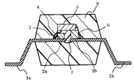
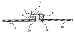
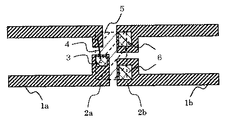
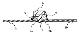
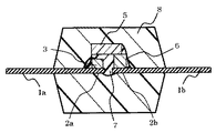
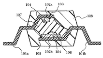
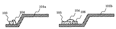
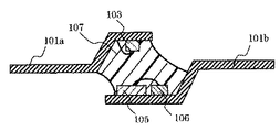
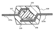
図1に本実施形態の光半導体装置の断面図を示す。図に示すように、発光側リードフレーム1aのベッド2a(発光側素子搭載部)上に発光素子3が載置・接続され、ワイヤー4により他方のリードフレームとボンディングされている。そして、この発光素子3と対向するように受光素子5が配置されている。受光素子5は、受光側リードフレーム1bのベッド2b(受光側素子搭載部)上に載置・接続されたMOSFET6とFCB(フリップチップボンディング)などにより接続され、これにより支持されている。発光素子3と受光素子5は光透過性の1次封止樹脂7で封止され、光の伝達経路が形成されており、さらに光遮断性の2次封止樹脂8で封止されている。
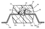
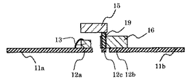
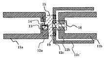
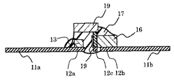
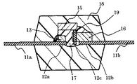
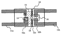
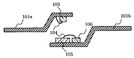
図5に本実施形態の光半導体装置を示す。図に示すように、実施形態1と同様に、発光側リードフレーム11aのベッド12a(発光側素子搭載部)上に発光素子13が載置・接続され、ワイヤー14によりボンディングされている。そしてこの発光素子13と対向するように受光素子15が配置されている。受光素子15は、受光側リードフレーム11bのベッド12b(受光側素子搭載部)上に載置・接続されたMOSFET16上で、ベッド12a、ベッド12b間に設けられた導電性のベッド12c上に載置された導電性のダミーペレット19により支持されている。ベッド12cはMOSFET16と接続されており、ダミーペレット19を経て受光素子15と接続されている。そして、実施形態1と同様に、発光素子13と受光素子15は光透過性の1次封止樹脂17で封止され、さらに光遮断性の2次封止樹脂18で封止されている。
2a、2b、12a、12b、12c、102a、102b ベッド
12c’ フレーム
3、13、103 発光素子
4、14、104 ワイヤー
5、15、105 受光素子
6、16、106 MOSFET
7、17、107 一次封止樹脂
8、18、108 二次封止樹脂
19 ダミーペレット
Claims (5)
- 発光側及び受光側のリードフレームと、
前記発光側及び受光側のリードフレームの一部及び/又はその近傍で、実質的に同一平面上に形成される発光側及び受光側の素子搭載部と、
発光側の前記素子搭載部上の所定位置に載置される発光素子と、
前記発光素子と対向するように設置される受光素子と、
受光側の前記素子搭載部上に配置され、前記発光素子から所定距離となるように、所定面において前記受光素子を支持する受光素子支持手段を備えることを特徴とする光半導体装置。 - 前記受光素子支持手段は、ダミーペレット及び/又は前記受光素子を制御する制御素子ペレットであることを特徴とする請求項1記載の光半導体装置。
- 前記受光素子支持手段は、前記受光素子を前記発光素子と対向する面において支持することを特徴とする請求項1又は2に記載の光半導体装置。
- 発光側リードフレーム及び受光側リードフレームの一部及び/又はその近傍に形成される発光側及び受光側の素子搭載部を、実質的に同一平面となるように配置する工程と、
発光素子を前記発光側の素子搭載部に載置する工程と、
受光素子支持手段を受光側の素子搭載部に載置する工程と、
受光素子を受光素子支持手段の所定面に設置し、前記発光素子と対向するように配置する工程を備えることを特徴とする光半導体装置の製造方法。 - 少なくとも前記発光素子及び前記受光素子を樹脂封止する工程と、
樹脂封止の後、前記受光側素子搭載部及び/又は受光素子支持手段の一部を除去する工程を備えることを特徴とする請求項4に記載の光半導体装置の製造方法。
Priority Applications (3)
| Application Number | Priority Date | Filing Date | Title |
|---|---|---|---|
| JP2004106772A JP2005294494A (ja) | 2004-03-31 | 2004-03-31 | 光半導体装置及びその製造方法 |
| US11/094,301 US7170099B2 (en) | 2004-03-31 | 2005-03-31 | Optical semiconductor device and a method for manufacturing the same |
| US11/615,170 US7307285B2 (en) | 2004-03-31 | 2006-12-22 | Optical semiconductor device and a method for manufacturing the same |
Applications Claiming Priority (1)
| Application Number | Priority Date | Filing Date | Title |
|---|---|---|---|
| JP2004106772A JP2005294494A (ja) | 2004-03-31 | 2004-03-31 | 光半導体装置及びその製造方法 |
Publications (1)
| Publication Number | Publication Date |
|---|---|
| JP2005294494A true JP2005294494A (ja) | 2005-10-20 |
Family
ID=35053362
Family Applications (1)
| Application Number | Title | Priority Date | Filing Date |
|---|---|---|---|
| JP2004106772A Pending JP2005294494A (ja) | 2004-03-31 | 2004-03-31 | 光半導体装置及びその製造方法 |
Country Status (2)
| Country | Link |
|---|---|
| US (2) | US7170099B2 (ja) |
| JP (1) | JP2005294494A (ja) |
Cited By (3)
| Publication number | Priority date | Publication date | Assignee | Title |
|---|---|---|---|---|
| CN107275436A (zh) * | 2013-09-12 | 2017-10-20 | 株式会社东芝 | 安装部件和光耦合器 |
| JP2023044783A (ja) * | 2021-09-21 | 2023-04-03 | 株式会社東芝 | 半導体装置 |
| JP2023176187A (ja) * | 2022-05-31 | 2023-12-13 | 株式会社東芝 | 半導体装置 |
Families Citing this family (11)
| Publication number | Priority date | Publication date | Assignee | Title |
|---|---|---|---|---|
| JP4796293B2 (ja) * | 2004-11-04 | 2011-10-19 | 株式会社 日立ディスプレイズ | 照明装置の製造方法 |
| US7736070B2 (en) * | 2005-08-31 | 2010-06-15 | Avago Technologies Ecbu Ip (Singapore) Pte. Ltd. | Double mold optocoupler |
| US8044412B2 (en) | 2006-01-20 | 2011-10-25 | Taiwan Semiconductor Manufacturing Company, Ltd | Package for a light emitting element |
| JP2008091671A (ja) * | 2006-10-03 | 2008-04-17 | Toshiba Corp | 光結合装置 |
| US20100116970A1 (en) * | 2008-11-12 | 2010-05-13 | Wen-Long Chou | Photo detection device |
| US8265487B2 (en) * | 2009-07-29 | 2012-09-11 | Avago Technologies Fiber Ip (Singapore) Pte. Ltd. | Half-duplex, single-fiber (S-F) optical transceiver module and method |
| CN101834267B (zh) * | 2010-04-30 | 2013-07-10 | 深圳市奥伦德元器件有限公司 | 平面支架及封装方法 |
| JP2016018832A (ja) * | 2014-07-07 | 2016-02-01 | パナソニックIpマネジメント株式会社 | 光結合装置 |
| JP6445947B2 (ja) * | 2015-09-04 | 2018-12-26 | 株式会社東芝 | 光結合装置 |
| DE102020121656A1 (de) * | 2020-08-18 | 2022-02-24 | OSRAM Opto Semiconductors Gesellschaft mit beschränkter Haftung | Verfahren zum herstellen eines optoelektronischen bauelements und optoelektronisches bauelement |
| WO2023168701A1 (zh) * | 2022-03-11 | 2023-09-14 | 开发晶照明(厦门)有限公司 | 光耦合装置 |
Family Cites Families (30)
| Publication number | Priority date | Publication date | Assignee | Title |
|---|---|---|---|---|
| JPS584470B2 (ja) * | 1975-04-02 | 1983-01-26 | 株式会社日立製作所 | ヒカリケツゴウハンドウタイソウチ オヨビ ソノセイホウ |
| JPS59177978A (ja) * | 1983-03-26 | 1984-10-08 | Nec Corp | マルチチヤンネル型半導体光結合装置 |
| US5148243A (en) * | 1985-06-25 | 1992-09-15 | Hewlett-Packard Company | Optical isolator with encapsulation |
| US5049527A (en) * | 1985-06-25 | 1991-09-17 | Hewlett-Packard Company | Optical isolator |
| DE3633251A1 (de) * | 1986-09-30 | 1988-03-31 | Siemens Ag | Optoelektronisches koppelelement |
| DE69408558T2 (de) * | 1993-05-28 | 1998-07-23 | Toshiba Ave Kk | Verwendung einer anisotropischen leitfähigen Schicht für die Verbindung von Anschlussleitern einer Leiterplatte mit den elektrischen Anschlusskontakten einer photoelektrischen Umwandlungsvorrichtung und Verfahren zur Montage dieser Vorrichtung |
| JP3349577B2 (ja) * | 1993-12-30 | 2002-11-25 | セイコーエプソン株式会社 | 印字装置 |
| JP3176496B2 (ja) * | 1993-12-27 | 2001-06-18 | シャープ株式会社 | 光結合装置およびその製造方法 |
| US5647034A (en) * | 1994-10-03 | 1997-07-08 | Matsushita Electric Works, Ltd. | Operation displaying semiconductor switch |
| DE4439838C2 (de) * | 1994-11-08 | 1999-02-25 | Telefunken Microelectron | Gabelkoppler |
| JPH08222757A (ja) * | 1995-02-14 | 1996-08-30 | Sharp Corp | 光結合素子 |
| JPH09148620A (ja) * | 1995-09-20 | 1997-06-06 | Sharp Corp | 光反射型検出器及びその製造方法 |
| US5753929A (en) * | 1996-08-28 | 1998-05-19 | Motorola, Inc. | Multi-directional optocoupler and method of manufacture |
| JPH11195973A (ja) * | 1998-01-07 | 1999-07-21 | Oki Electric Ind Co Ltd | 半導体装置及びそれを用いた双方向光mosリレー |
| JPH11204825A (ja) | 1998-01-14 | 1999-07-30 | Oki Electric Ind Co Ltd | 光半導体装置およびその製造方法 |
| US6051848A (en) * | 1998-03-02 | 2000-04-18 | Motorola, Inc. | Optical device packages containing an optical transmitter die |
| US6864227B1 (en) * | 1998-04-13 | 2005-03-08 | California Institute Of Technology | Artery-and vein-specific proteins and uses therefor |
| US6393183B1 (en) * | 1998-08-13 | 2002-05-21 | Eugene Robert Worley | Opto-coupler device for packaging optically coupled integrated circuits |
| EP1020933B1 (en) * | 1999-01-13 | 2003-05-02 | Sharp Kabushiki Kaisha | Photocoupler device |
| JP2001059923A (ja) * | 1999-06-16 | 2001-03-06 | Seiko Epson Corp | 光モジュール及びその製造方法、半導体装置並びに光伝達装置 |
| JP3502305B2 (ja) * | 1999-08-13 | 2004-03-02 | Nec化合物デバイス株式会社 | 光半導体装置 |
| JP4117868B2 (ja) * | 1999-11-22 | 2008-07-16 | シャープ株式会社 | 光結合素子 |
| US6770867B2 (en) * | 2001-06-29 | 2004-08-03 | Fei Company | Method and apparatus for scanned instrument calibration |
| JP3781180B2 (ja) * | 2001-05-15 | 2006-05-31 | シャープ株式会社 | 光結合素子を製造する製造装置、およびその製造方法 |
| JP2003008050A (ja) | 2001-06-26 | 2003-01-10 | Matsushita Electric Works Ltd | 半導体リレー |
| JP3938479B2 (ja) * | 2001-07-18 | 2007-06-27 | シャープ株式会社 | 光結合素子の生産システム |
| US6885016B2 (en) * | 2001-09-04 | 2005-04-26 | Eugene Robert Worley | Switching power supply circuit using a silicon based LED for feedback |
| JP2003282935A (ja) * | 2002-03-26 | 2003-10-03 | Sharp Corp | 光結合素子、その製造方法、及び電子機器 |
| US6919625B2 (en) * | 2003-07-10 | 2005-07-19 | General Semiconductor, Inc. | Surface mount multichip devices |
| JP4282392B2 (ja) * | 2003-07-11 | 2009-06-17 | 株式会社東芝 | 光半導体装置及びその製造方法 |
-
2004
- 2004-03-31 JP JP2004106772A patent/JP2005294494A/ja active Pending
-
2005
- 2005-03-31 US US11/094,301 patent/US7170099B2/en not_active Expired - Fee Related
-
2006
- 2006-12-22 US US11/615,170 patent/US7307285B2/en not_active Expired - Fee Related
Cited By (6)
| Publication number | Priority date | Publication date | Assignee | Title |
|---|---|---|---|---|
| CN107275436A (zh) * | 2013-09-12 | 2017-10-20 | 株式会社东芝 | 安装部件和光耦合器 |
| CN107275436B (zh) * | 2013-09-12 | 2019-04-30 | 株式会社东芝 | 安装部件和光耦合器 |
| JP2023044783A (ja) * | 2021-09-21 | 2023-04-03 | 株式会社東芝 | 半導体装置 |
| JP7566708B2 (ja) | 2021-09-21 | 2024-10-15 | 株式会社東芝 | 半導体装置 |
| JP2023176187A (ja) * | 2022-05-31 | 2023-12-13 | 株式会社東芝 | 半導体装置 |
| JP7712894B2 (ja) | 2022-05-31 | 2025-07-24 | 株式会社東芝 | 半導体装置 |
Also Published As
| Publication number | Publication date |
|---|---|
| US7307285B2 (en) | 2007-12-11 |
| US7170099B2 (en) | 2007-01-30 |
| US20050218492A1 (en) | 2005-10-06 |
| US20070102712A1 (en) | 2007-05-10 |
Similar Documents
| Publication | Publication Date | Title |
|---|---|---|
| KR100604190B1 (ko) | 고체촬상장치, 반도체 웨이퍼, 광학장치용 모듈,고체촬상장치의 제조방법, 및 광학장치용 모듈의 제조방법 | |
| US7838899B2 (en) | Integrated circuit package system with image sensor system | |
| US6909168B2 (en) | Resin encapsulation semiconductor device utilizing grooved leads and die pad | |
| JP2005294494A (ja) | 光半導体装置及びその製造方法 | |
| KR101579623B1 (ko) | 이미지 센서용 반도체 패키지 및 그 제조 방법 | |
| JP2007142042A (ja) | 半導体パッケージとその製造方法,半導体モジュール,および電子機器 | |
| KR20090017961A (ko) | 화상센서 패키지 및 그 형성 방법 | |
| JP2006332680A (ja) | イメージセンサをパッケージングするための方法及びパッケージングされたイメージセンサ | |
| CN107546194A (zh) | 用于具有玻璃顶盖的混合式光学封装的结构和方法 | |
| US8003426B2 (en) | Method for manufacturing package structure of optical device | |
| JP4925832B2 (ja) | 光センサを実装するための方法 | |
| JP2009193986A (ja) | 半導体装置及びその製造方法 | |
| JP2006179718A (ja) | 青色光学素子パッケージ及び光学素子パッケージの製造方法 | |
| JP2009176894A (ja) | 光学半導体装置 | |
| JP4282392B2 (ja) | 光半導体装置及びその製造方法 | |
| CN101567333A (zh) | 图像感测装置及其封装方法 | |
| JP4466552B2 (ja) | 固体撮像装置の製造方法 | |
| JP2006005612A (ja) | 撮像モジュール | |
| US20070057149A1 (en) | Image sensor chip package fabrication method | |
| JP2005327967A (ja) | 半導体装置 | |
| US20110241191A1 (en) | Semiconductor lamination package and method of producing semiconductor lamination package | |
| JP2008026183A (ja) | Ic一体型加速度センサ | |
| JP2010040826A (ja) | 半導体チップおよびその製造方法 | |
| KR101926721B1 (ko) | 반도체 패키지 및 그 제조방법 | |
| JP2006278743A (ja) | 固体撮像装置 |
Legal Events
| Date | Code | Title | Description |
|---|---|---|---|
| A621 | Written request for application examination |
Free format text: JAPANESE INTERMEDIATE CODE: A621 Effective date: 20060424 |
|
| RD04 | Notification of resignation of power of attorney |
Free format text: JAPANESE INTERMEDIATE CODE: A7424 Effective date: 20060427 |
|
| A977 | Report on retrieval |
Free format text: JAPANESE INTERMEDIATE CODE: A971007 Effective date: 20080916 |
|
| A131 | Notification of reasons for refusal |
Free format text: JAPANESE INTERMEDIATE CODE: A131 Effective date: 20080930 |
|
| A02 | Decision of refusal |
Free format text: JAPANESE INTERMEDIATE CODE: A02 Effective date: 20090217 |