JP2005294494A - Optical semiconductor device and manufacturing method thereof - Google Patents
Optical semiconductor device and manufacturing method thereof Download PDFInfo
- Publication number
- JP2005294494A JP2005294494A JP2004106772A JP2004106772A JP2005294494A JP 2005294494 A JP2005294494 A JP 2005294494A JP 2004106772 A JP2004106772 A JP 2004106772A JP 2004106772 A JP2004106772 A JP 2004106772A JP 2005294494 A JP2005294494 A JP 2005294494A
- Authority
- JP
- Japan
- Prior art keywords
- light receiving
- light emitting
- light
- receiving element
- optical semiconductor
- Prior art date
- Legal status (The legal status is an assumption and is not a legal conclusion. Google has not performed a legal analysis and makes no representation as to the accuracy of the status listed.)
- Pending
Links
Images
Classifications
-
- H—ELECTRICITY
- H10—SEMICONDUCTOR DEVICES; ELECTRIC SOLID-STATE DEVICES NOT OTHERWISE PROVIDED FOR
- H10W—GENERIC PACKAGES, INTERCONNECTIONS, CONNECTORS OR OTHER CONSTRUCTIONAL DETAILS OF DEVICES COVERED BY CLASS H10
- H10W90/00—Package configurations
-
- H—ELECTRICITY
- H10—SEMICONDUCTOR DEVICES; ELECTRIC SOLID-STATE DEVICES NOT OTHERWISE PROVIDED FOR
- H10W—GENERIC PACKAGES, INTERCONNECTIONS, CONNECTORS OR OTHER CONSTRUCTIONAL DETAILS OF DEVICES COVERED BY CLASS H10
- H10W90/00—Package configurations
- H10W90/701—Package configurations characterised by the relative positions of pads or connectors relative to package parts
- H10W90/751—Package configurations characterised by the relative positions of pads or connectors relative to package parts of bond wires
- H10W90/756—Package configurations characterised by the relative positions of pads or connectors relative to package parts of bond wires between a chip and a stacked lead frame, conducting package substrate or heat sink
Landscapes
- Photo Coupler, Interrupter, Optical-To-Optical Conversion Devices (AREA)
Abstract
【課題】 パッケージの小型化、及び工程数の削減を図ることが可能な光半導体装置及びその製造方法を提供する。
【解決手段】 発光側及び受光側のリードフレーム1と、前記発光側及び受光側のリードフレームの一部及び/又はその近傍で、実質的に同一平面上に形成される発光側及び受光側の素子搭載部2と、発光側の前記素子搭載部2a上の所定位置に載置される発光素子3と、前記発光素子と対向するように設置される受光素子5と、受光側の前記素子搭載部2b上に配置され、前記発光素子3から所定距離となるように、所定面において前記受光素子5を支持する受光素子支持手段6を備える。
【選択図】 図1PROBLEM TO BE SOLVED: To provide an optical semiconductor device capable of reducing the size of a package and reducing the number of processes and a method for manufacturing the same.
A light emitting side and a light receiving side lead frame 1 and a part of and / or in the vicinity of the light emitting side and the light receiving side lead frame are formed on substantially the same plane. An element mounting portion 2, a light emitting element 3 placed at a predetermined position on the light emitting side element mounting portion 2a, a light receiving element 5 installed so as to face the light emitting element, and the element mounting on the light receiving side The light receiving element support means 6 is provided on the predetermined surface to support the light receiving element 5 so as to be disposed at a predetermined distance from the light emitting element 3.
[Selection] Figure 1
Description
本発明は、発光素子と受光素子が対向配置する構造を有する光半導体装置及びその製造方法に関する。 The present invention relates to an optical semiconductor device having a structure in which a light emitting element and a light receiving element are arranged to face each other, and a method for manufacturing the same.
一般に、フォトカプラ、フォトリレー等光半導体装置においては、発光素子(発光ダイオード)、受光素子(光起電ダイオード)及び駆動用のMOSFETを夫々リードフレームに搭載し、発光素子と受光素子が対向するように配置して封止する構造が用いられている(例えば特許文献1参照)。 Generally, in an optical semiconductor device such as a photocoupler or a photorelay, a light emitting element (light emitting diode), a light receiving element (photovoltaic diode), and a driving MOSFET are mounted on a lead frame, respectively, and the light emitting element and the light receiving element face each other. Such a structure that is arranged and sealed is used (see, for example, Patent Document 1).
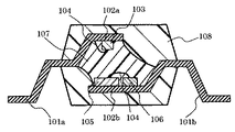
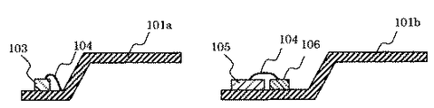
図10に従来の光半導体装置を二重封止構造のフォトリレーを例に挙げて示す。図に示すように、発光側リードフレーム101aに発光素子103が、受光側リードフレーム101bに受光素子105及びMOSFET106が搭載されており、これらが対向するように配置されている。これら素子は光透過性樹脂107で1次封止、光遮断性樹脂108で2次封止されている。発光素子、受光素子は夫々リードフレーム、MOSFETとワイヤー104によりボンディングされている。
FIG. 10 shows a conventional optical semiconductor device taking a double-sealed photorelay as an example. As shown in the figure, the
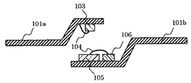
このようなフォトカプラは、以下のように形成される。先ず、図11に示すように、夫々押し下げ加工されたリードフレーム101a、101bに、夫々発光素子103、受光素子105/MOSFET106を搭載する。そして、図12に示すように、これらを対向させた状態に配置する。
Such a photocoupler is formed as follows. First, as shown in FIG. 11, the light-emitting
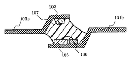
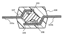
次に、図13に示すように、これらを光透過性樹脂107により1次封止し、光の伝達経路を形成する。そして、図14に示すように、光を遮断し、素子を保護するために、光遮断性樹脂108により2次封止する。さらに各リードフレーム101a、101bをフォーミングして、図10に示す光半導体素子が形成される。
近年、半導体装置の高性能化、実装密度の向上に伴い、光半導体装置の小型化が強く要求されている。しかしながら、このような従来の光半導体装置においては、上述したとおり、受光側リードフレームにおいて、受光素子とMOSFETを平面配置しているため、パッケージの小型化が困難であるという問題があった。 In recent years, there has been a strong demand for miniaturization of optical semiconductor devices as the performance of semiconductor devices increases and the packaging density increases. However, such a conventional optical semiconductor device has a problem that it is difficult to reduce the size of the package because the light receiving element and the MOSFET are arranged in a plane in the light receiving side lead frame as described above.
また、従来の製造工程においては、発光側、受光側のリードフレームを対向させる工程、さらにこれを保持した上で封止する工程を要しており、工程数の削減によるリードタイムの短縮やコストの削減が困難であるという問題があった。 In addition, the conventional manufacturing process requires a process of facing the lead frame on the light emitting side and the light receiving side, and a process of holding and holding the lead frame, thereby reducing the lead time and cost by reducing the number of processes. There was a problem that it was difficult to reduce.
そこで、本発明は、従来の問題を取り除き、パッケージの小型化、及び工程数の削減を図ることが可能な光半導体装置及びその製造方法を提供することを目的とするものである。 Accordingly, an object of the present invention is to provide an optical semiconductor device and a method for manufacturing the same, which can eliminate the conventional problems and can reduce the size of the package and the number of processes.
本発明の一態様によれば、発光側及び受光側のリードフレームと、前記発光側及び受光側のリードフレームの一部及び/又はその近傍で、実質的に同一平面上に形成される発光側及び受光側の素子搭載部と、発光側の前記素子搭載部上の所定位置に載置される発光素子と、前記発光素子と対向するように設置される受光素子と、受光側の前記素子搭載部上に配置され、前記発光素子から所定距離となるように、所定面において前記受光素子を支持する受光素子支持手段を備えることを特徴とする光半導体装置が提供される。 According to one aspect of the present invention, a light emitting side and a light receiving side lead frame, and a light emitting side formed substantially on the same plane in a part of and / or in the vicinity of the light emitting side and light receiving side lead frames. And a light receiving element mounting portion, a light emitting element mounted at a predetermined position on the light emitting element mounting portion, a light receiving element installed to face the light emitting element, and the light receiving element mounting. There is provided an optical semiconductor device comprising: a light receiving element supporting unit that is disposed on the part and supports the light receiving element on a predetermined surface so as to be a predetermined distance from the light emitting element.
また、本発明の一態様によれば、発光側リードフレーム及び受光側リードフレームの一部及び/又はその近傍に形成される発光側及び受光側の素子搭載部を、実質的に同一平面となるように配置する工程と、発光素子を前記発光側の素子搭載部に載置する工程と、受光素子支持手段を受光側の素子搭載部に載置する工程と、受光素子を受光素子支持手段の所定面に設置し、前記発光素子と対向するように配置する工程を備えることを特徴とする光半導体装置の製造方法が提供される。 Also, according to one aspect of the present invention, the light emitting side and light receiving side element mounting portions formed in part of and / or in the vicinity of the light emitting side lead frame and the light receiving side lead frame are substantially flush with each other. The step of placing the light emitting element on the light emitting side element mounting portion, the step of placing the light receiving element supporting means on the light receiving side element mounting portion, and the light receiving element of the light receiving element supporting means. There is provided a method for manufacturing an optical semiconductor device, comprising a step of disposing the light-emitting element on a predetermined surface so as to face the light-emitting element.
本発明の一実施態様によれば、パッケージの小型化、及び工程数の削減を図ることが可能な光半導体装置及びその製造方法を提供することができる。 According to one embodiment of the present invention, it is possible to provide an optical semiconductor device capable of reducing the size of the package and reducing the number of processes, and a method for manufacturing the same.
以下本発明の実施形態について、図を参照して説明する。 Embodiments of the present invention will be described below with reference to the drawings.
(実施形態1)
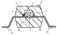
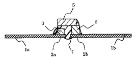
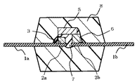
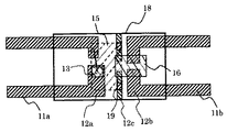
図1に本実施形態の光半導体装置の断面図を示す。図に示すように、発光側リードフレーム1aのベッド2a(発光側素子搭載部)上に発光素子3が載置・接続され、ワイヤー4により他方のリードフレームとボンディングされている。そして、この発光素子3と対向するように受光素子5が配置されている。受光素子5は、受光側リードフレーム1bのベッド2b(受光側素子搭載部)上に載置・接続されたMOSFET6とFCB(フリップチップボンディング)などにより接続され、これにより支持されている。発光素子3と受光素子5は光透過性の1次封止樹脂7で封止され、光の伝達経路が形成されており、さらに光遮断性の2次封止樹脂8で封止されている。
(Embodiment 1)
FIG. 1 is a cross-sectional view of the optical semiconductor device of this embodiment. As shown in the figure, the
そして、このような光半導体装置において、リードフレーム1aより外部からの電気信号が入力され、発光素子3が発光し、1次封止樹脂7を介して受光素子5に光信号が伝達される。そして、受光素子5において電気信号に変換され、MOSFET6を経て、リードフレーム1bより出力される。
In such an optical semiconductor device, an external electrical signal is input from the lead frame 1 a, the
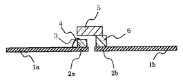
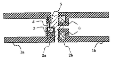
このような光半導体装置は、例えば以下のように形成される。先ず、図2−aに断面図を、図2−bに上面図を示すように、プレス、エッチングなどにより発光側と受光側が所定の間隔となるように形成され、一体化されたリードフレーム1a、1bを用い、ベッド2a上に発光素子3を、ベッド2b上にMOSFET6を夫々載置、接続する。そして、MOSFET6上に、受光素子5をその一部が発光素子3と対向するように載置する。
Such an optical semiconductor device is formed as follows, for example. First, as shown in a cross-sectional view in FIG. 2-a and a top view in FIG. 2-b, the lead frame 1a is formed by pressing, etching, or the like so that the light-emitting side and the light-receiving side are spaced at a predetermined interval. 1b is used to place and connect the
次いで、図3に示すように、発光素子3、受光素子5を光透過性の1次封止樹脂7で封止し、光の伝達経路を形成する。そして、図4に示すように、これらを光遮断性の2次封止樹脂8で封止する。さらに、封止樹脂8から露出したリードフレーム1a、1bを、実装用にフォーミングし、図1に示す光半導体装置が形成される。
Next, as shown in FIG. 3, the light-emitting
このような光半導体素子においては、従来平面配置されていた受光素子とMOSFETを立体的に配置することができ、パッケージの小型化を実現することが可能となる。さらに、発光素子と受光素子は、発光側、受光側が同一平面上に配置されたリードフレーム上に搭載されるため、従来の1次封止前の、発光側、受光側リードフレームを対向・保持する接合工程を省略することができ、工程数の削減が可能となる。また、高さ方向の位置制御も容易となり、さらに発光側と受光側が一体化したリードフレームを用いているため、フレーム方向の位置ずれが抑制され、特性のばらつきも抑えられる。 In such an optical semiconductor element, the light receiving element and the MOSFET, which are conventionally arranged in a plane, can be three-dimensionally arranged, and the package can be downsized. Furthermore, since the light emitting element and the light receiving element are mounted on a lead frame in which the light emitting side and the light receiving side are arranged on the same plane, the light emitting side and the light receiving side lead frame are opposed and held before the conventional primary sealing. The joining step to be performed can be omitted, and the number of steps can be reduced. In addition, position control in the height direction is easy, and since a lead frame in which the light emitting side and the light receiving side are integrated is used, positional deviation in the frame direction is suppressed, and variations in characteristics are also suppressed.
(実施形態2)
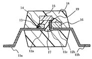
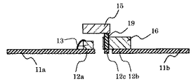
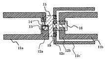
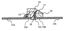
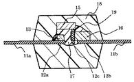
図5に本実施形態の光半導体装置を示す。図に示すように、実施形態1と同様に、発光側リードフレーム11aのベッド12a(発光側素子搭載部)上に発光素子13が載置・接続され、ワイヤー14によりボンディングされている。そしてこの発光素子13と対向するように受光素子15が配置されている。受光素子15は、受光側リードフレーム11bのベッド12b(受光側素子搭載部)上に載置・接続されたMOSFET16上で、ベッド12a、ベッド12b間に設けられた導電性のベッド12c上に載置された導電性のダミーペレット19により支持されている。ベッド12cはMOSFET16と接続されており、ダミーペレット19を経て受光素子15と接続されている。そして、実施形態1と同様に、発光素子13と受光素子15は光透過性の1次封止樹脂17で封止され、さらに光遮断性の2次封止樹脂18で封止されている。
(Embodiment 2)
FIG. 5 shows the optical semiconductor device of this embodiment. As shown in the figure, the
このような光半導体装置において、実施形態1と同様に、リードフレーム11aより外部からの電気信号が入力され、発光素子13が発光し、1次封止樹脂17を介して受光素子15に光信号が伝達される。そして、受光素子15において電気信号に変換され、MOSFET16を経て、リードフレーム11bより出力される。
In such an optical semiconductor device, as in the first embodiment, an external electrical signal is input from the
このような光半導体装置は、例えば以下のように形成される。先ず、図6−aに断面図を、図6−bに上面図を示すように、実施形態1と同様に、リードフレーム11a、11bの、ベッド12a上に発光素子13を、ベッド12b上にMOSFET16を夫々載置、接続する。一方、受光側リードフレーム11bの外周を囲むように形成されたフレーム12c’のベッド12cと、MOSFET16を接続し、これを挟むように、ベッド12c上にダミーペレット19を載置する。そして、ダミーペレット19上に、受光素子15を載置、接続し、発光素子13と対向させる。尚、リードフレーム11a、11b、フレーム12c’は、プレス、エッチングなどにより形成され、一体化されている。
Such an optical semiconductor device is formed as follows, for example. First, as shown in the cross-sectional view of FIG. 6A and the top view of FIG.
次いで、図7に示すように、発光素子13、受光素子15を光透過性の1次封止樹脂17で封止し、光の伝達経路を形成する。そして、図8に示すように、これらを光遮断性の2次封止樹脂18で封止する。
Next, as shown in FIG. 7, the light-emitting
次いで、図9に示すように、フレーム12c’の封止樹脂18から露出した部分を切断、除去する。そして、封止樹脂18から露出したリードフレーム11a、11bを、実装用にフォーミングし、図5に示す光半導体装置が形成される。
Next, as shown in FIG. 9, the portion exposed from the sealing
本実施形態において、ダミーペレットの材料を特に規定していないが、内部素子のデザインにより、セラミックス系、シリコン系、金属系等、導電性、非導電性の種々の材料を適宜選択することが可能である。 In this embodiment, the material of the dummy pellet is not particularly specified, but various conductive and non-conductive materials such as ceramics, silicons, and metals can be appropriately selected depending on the design of the internal element. It is.
尚、これら実施形態において、発光側、受光側が一体化されたリードフレームが用いられているが、必ずしも一体化されていなくてもよく、夫々形成されたものを同一平面上に位置制御して配置しても良い。また、HOOP状フレームを用いて、連続的に形成することも可能である。 In these embodiments, a lead frame in which the light emitting side and the light receiving side are integrated is used. However, the lead frame does not necessarily have to be integrated, and the formed ones are positioned and controlled on the same plane. You may do it. It is also possible to form continuously using a HOOP-like frame.
また、ベッド上における各素子の接続方法は特に規定されないが、樹脂接合、共晶接合や、FCB等適宜選択することができる。 The connection method of each element on the bed is not particularly defined, but can be appropriately selected from resin bonding, eutectic bonding, FCB, and the like.
これら実施形態においては、MOSFETを搭載しているが、MOSFETを有さない光半導体素子においても、ダミーペレット上に受光素子を載置することで、工程数の削減や、特性のばらつきの抑制、パッケージの小型化等の効果を得ることができる。そして、ダミーペレットは、樹脂封止後においても必ずしもベッド上に固定されている必要はなく、樹脂封止後にベッドが除去されていてもよい。 In these embodiments, a MOSFET is mounted, but even in an optical semiconductor element that does not have a MOSFET, by placing a light receiving element on a dummy pellet, the number of processes can be reduced, and variation in characteristics can be suppressed. Effects such as downsizing of the package can be obtained. And the dummy pellet does not necessarily need to be fixed on the bed even after resin sealing, and the bed may be removed after resin sealing.
尚、本発明は、上述した実施形態に限定されるものではない。その他要旨を逸脱しない範囲で種々変形して実施することができる。 In addition, this invention is not limited to embodiment mentioned above. Various other modifications can be made without departing from the scope of the invention.
1a、1b、11a、11b、101a、101b リードフレーム
2a、2b、12a、12b、12c、102a、102b ベッド
12c’ フレーム
3、13、103 発光素子
4、14、104 ワイヤー
5、15、105 受光素子
6、16、106 MOSFET
7、17、107 一次封止樹脂
8、18、108 二次封止樹脂
19 ダミーペレット
1a, 1b, 11a, 11b, 101a,
7, 17, 107
Claims (5)
前記発光側及び受光側のリードフレームの一部及び/又はその近傍で、実質的に同一平面上に形成される発光側及び受光側の素子搭載部と、
発光側の前記素子搭載部上の所定位置に載置される発光素子と、
前記発光素子と対向するように設置される受光素子と、
受光側の前記素子搭載部上に配置され、前記発光素子から所定距離となるように、所定面において前記受光素子を支持する受光素子支持手段を備えることを特徴とする光半導体装置。 A lead frame on the light emitting side and the light receiving side;
A light emitting side and a light receiving side element mounting portion formed on substantially the same plane in a part of and / or in the vicinity of the light emitting side and light receiving side lead frames;
A light emitting element placed at a predetermined position on the element mounting portion on the light emitting side;
A light receiving element installed to face the light emitting element;
An optical semiconductor device comprising: a light receiving element supporting unit that is disposed on the element mounting portion on the light receiving side and supports the light receiving element on a predetermined surface so as to be a predetermined distance from the light emitting element.
発光素子を前記発光側の素子搭載部に載置する工程と、
受光素子支持手段を受光側の素子搭載部に載置する工程と、
受光素子を受光素子支持手段の所定面に設置し、前記発光素子と対向するように配置する工程を備えることを特徴とする光半導体装置の製造方法。 Arranging the light emitting side and light receiving side element mounting portions formed in a part of and / or in the vicinity of the light emitting side lead frame and the light receiving side lead frame so as to be substantially in the same plane;
Placing the light emitting element on the light emitting side element mounting portion;
Placing the light receiving element support means on the light receiving element mounting portion;
A method of manufacturing an optical semiconductor device, comprising: a step of installing a light receiving element on a predetermined surface of a light receiving element supporting unit and disposing the light receiving element so as to face the light emitting element.
樹脂封止の後、前記受光側素子搭載部及び/又は受光素子支持手段の一部を除去する工程を備えることを特徴とする請求項4に記載の光半導体装置の製造方法。 A step of resin-sealing at least the light emitting element and the light receiving element;
5. The method of manufacturing an optical semiconductor device according to claim 4, further comprising a step of removing a part of the light receiving side element mounting portion and / or the light receiving element support means after resin sealing.
Priority Applications (3)
| Application Number | Priority Date | Filing Date | Title |
|---|---|---|---|
| JP2004106772A JP2005294494A (en) | 2004-03-31 | 2004-03-31 | Optical semiconductor device and manufacturing method thereof |
| US11/094,301 US7170099B2 (en) | 2004-03-31 | 2005-03-31 | Optical semiconductor device and a method for manufacturing the same |
| US11/615,170 US7307285B2 (en) | 2004-03-31 | 2006-12-22 | Optical semiconductor device and a method for manufacturing the same |
Applications Claiming Priority (1)
| Application Number | Priority Date | Filing Date | Title |
|---|---|---|---|
| JP2004106772A JP2005294494A (en) | 2004-03-31 | 2004-03-31 | Optical semiconductor device and manufacturing method thereof |
Publications (1)
| Publication Number | Publication Date |
|---|---|
| JP2005294494A true JP2005294494A (en) | 2005-10-20 |
Family
ID=35053362
Family Applications (1)
| Application Number | Title | Priority Date | Filing Date |
|---|---|---|---|
| JP2004106772A Pending JP2005294494A (en) | 2004-03-31 | 2004-03-31 | Optical semiconductor device and manufacturing method thereof |
Country Status (2)
| Country | Link |
|---|---|
| US (2) | US7170099B2 (en) |
| JP (1) | JP2005294494A (en) |
Cited By (3)
| Publication number | Priority date | Publication date | Assignee | Title |
|---|---|---|---|---|
| CN107275436A (en) * | 2013-09-12 | 2017-10-20 | 株式会社东芝 | Installing component and photo-coupler |
| JP2023044783A (en) * | 2021-09-21 | 2023-04-03 | 株式会社東芝 | semiconductor equipment |
| JP2023176187A (en) * | 2022-05-31 | 2023-12-13 | 株式会社東芝 | semiconductor equipment |
Families Citing this family (11)
| Publication number | Priority date | Publication date | Assignee | Title |
|---|---|---|---|---|
| JP4796293B2 (en) * | 2004-11-04 | 2011-10-19 | 株式会社 日立ディスプレイズ | Manufacturing method of lighting device |
| US7736070B2 (en) * | 2005-08-31 | 2010-06-15 | Avago Technologies Ecbu Ip (Singapore) Pte. Ltd. | Double mold optocoupler |
| US8044412B2 (en) | 2006-01-20 | 2011-10-25 | Taiwan Semiconductor Manufacturing Company, Ltd | Package for a light emitting element |
| JP2008091671A (en) * | 2006-10-03 | 2008-04-17 | Toshiba Corp | Optical coupling device |
| US20100116970A1 (en) * | 2008-11-12 | 2010-05-13 | Wen-Long Chou | Photo detection device |
| US8265487B2 (en) * | 2009-07-29 | 2012-09-11 | Avago Technologies Fiber Ip (Singapore) Pte. Ltd. | Half-duplex, single-fiber (S-F) optical transceiver module and method |
| CN101834267B (en) * | 2010-04-30 | 2013-07-10 | 深圳市奥伦德元器件有限公司 | Planar bracket and encapsulating method |
| JP2016018832A (en) * | 2014-07-07 | 2016-02-01 | パナソニックIpマネジメント株式会社 | Optical coupling device |
| JP6445947B2 (en) * | 2015-09-04 | 2018-12-26 | 株式会社東芝 | Optical coupling device |
| DE102020121656A1 (en) * | 2020-08-18 | 2022-02-24 | OSRAM Opto Semiconductors Gesellschaft mit beschränkter Haftung | METHOD FOR MANUFACTURING OPTOELECTRONIC DEVICE AND OPTOELECTRONIC DEVICE |
| CN117425845A (en) * | 2022-03-11 | 2024-01-19 | 开发晶照明(厦门)有限公司 | Optical coupler |
Family Cites Families (30)
| Publication number | Priority date | Publication date | Assignee | Title |
|---|---|---|---|---|
| JPS584470B2 (en) * | 1975-04-02 | 1983-01-26 | 株式会社日立製作所 | Hikariketsugohandoutaisouchi Oyobi Sonoseihou |
| JPS59177978A (en) * | 1983-03-26 | 1984-10-08 | Nec Corp | Multi-channel semiconductor optical coupler |
| US5148243A (en) * | 1985-06-25 | 1992-09-15 | Hewlett-Packard Company | Optical isolator with encapsulation |
| US5049527A (en) * | 1985-06-25 | 1991-09-17 | Hewlett-Packard Company | Optical isolator |
| DE3633251A1 (en) * | 1986-09-30 | 1988-03-31 | Siemens Ag | OPTOELECTRONIC COUPLING ELEMENT |
| DE69408558T2 (en) * | 1993-05-28 | 1998-07-23 | Toshiba Ave Kk | Use of an anisotropic conductive layer for connecting connection conductors of a printed circuit board to the electrical connection contacts of a photoelectric conversion device and method for assembling this device |
| JP3349577B2 (en) * | 1993-12-30 | 2002-11-25 | セイコーエプソン株式会社 | Printing device |
| JP3176496B2 (en) * | 1993-12-27 | 2001-06-18 | シャープ株式会社 | Optical coupling device and method of manufacturing the same |
| US5647034A (en) * | 1994-10-03 | 1997-07-08 | Matsushita Electric Works, Ltd. | Operation displaying semiconductor switch |
| DE4439838C2 (en) * | 1994-11-08 | 1999-02-25 | Telefunken Microelectron | Fork coupler |
| JPH08222757A (en) | 1995-02-14 | 1996-08-30 | Sharp Corp | Optical coupling element |
| JPH09148620A (en) * | 1995-09-20 | 1997-06-06 | Sharp Corp | Light reflection type detector and manufacturing method thereof |
| US5753929A (en) * | 1996-08-28 | 1998-05-19 | Motorola, Inc. | Multi-directional optocoupler and method of manufacture |
| JPH11195973A (en) | 1998-01-07 | 1999-07-21 | Oki Electric Ind Co Ltd | Semiconductor device and bidirectional optical MOS relay using the same |
| JPH11204825A (en) | 1998-01-14 | 1999-07-30 | Oki Electric Ind Co Ltd | Optical semiconductor device and method for manufacturing the same |
| US6051848A (en) * | 1998-03-02 | 2000-04-18 | Motorola, Inc. | Optical device packages containing an optical transmitter die |
| US6864227B1 (en) * | 1998-04-13 | 2005-03-08 | California Institute Of Technology | Artery-and vein-specific proteins and uses therefor |
| US6393183B1 (en) * | 1998-08-13 | 2002-05-21 | Eugene Robert Worley | Opto-coupler device for packaging optically coupled integrated circuits |
| EP1020933B1 (en) * | 1999-01-13 | 2003-05-02 | Sharp Kabushiki Kaisha | Photocoupler device |
| JP2001059923A (en) * | 1999-06-16 | 2001-03-06 | Seiko Epson Corp | Optical module and manufacturing method thereof, semiconductor device, and optical transmission device |
| JP3502305B2 (en) * | 1999-08-13 | 2004-03-02 | Nec化合物デバイス株式会社 | Optical semiconductor device |
| JP4117868B2 (en) | 1999-11-22 | 2008-07-16 | シャープ株式会社 | Optical coupling element |
| US6770867B2 (en) * | 2001-06-29 | 2004-08-03 | Fei Company | Method and apparatus for scanned instrument calibration |
| JP3781180B2 (en) | 2001-05-15 | 2006-05-31 | シャープ株式会社 | Manufacturing apparatus for manufacturing optical coupling element and manufacturing method thereof |
| JP2003008050A (en) | 2001-06-26 | 2003-01-10 | Matsushita Electric Works Ltd | Semiconductor relay |
| JP3938479B2 (en) * | 2001-07-18 | 2007-06-27 | シャープ株式会社 | Optocoupler production system |
| US6885016B2 (en) * | 2001-09-04 | 2005-04-26 | Eugene Robert Worley | Switching power supply circuit using a silicon based LED for feedback |
| JP2003282935A (en) * | 2002-03-26 | 2003-10-03 | Sharp Corp | Optical coupling element, method for manufacturing the same, and electronic device |
| US6919625B2 (en) * | 2003-07-10 | 2005-07-19 | General Semiconductor, Inc. | Surface mount multichip devices |
| JP4282392B2 (en) | 2003-07-11 | 2009-06-17 | 株式会社東芝 | Optical semiconductor device and manufacturing method thereof |
-
2004
- 2004-03-31 JP JP2004106772A patent/JP2005294494A/en active Pending
-
2005
- 2005-03-31 US US11/094,301 patent/US7170099B2/en not_active Expired - Fee Related
-
2006
- 2006-12-22 US US11/615,170 patent/US7307285B2/en not_active Expired - Fee Related
Cited By (6)
| Publication number | Priority date | Publication date | Assignee | Title |
|---|---|---|---|---|
| CN107275436A (en) * | 2013-09-12 | 2017-10-20 | 株式会社东芝 | Installing component and photo-coupler |
| CN107275436B (en) * | 2013-09-12 | 2019-04-30 | 株式会社东芝 | Mounting parts and optocouplers |
| JP2023044783A (en) * | 2021-09-21 | 2023-04-03 | 株式会社東芝 | semiconductor equipment |
| JP7566708B2 (en) | 2021-09-21 | 2024-10-15 | 株式会社東芝 | Semiconductor Device |
| JP2023176187A (en) * | 2022-05-31 | 2023-12-13 | 株式会社東芝 | semiconductor equipment |
| JP7712894B2 (en) | 2022-05-31 | 2025-07-24 | 株式会社東芝 | Semiconductor Device |
Also Published As
| Publication number | Publication date |
|---|---|
| US20070102712A1 (en) | 2007-05-10 |
| US20050218492A1 (en) | 2005-10-06 |
| US7307285B2 (en) | 2007-12-11 |
| US7170099B2 (en) | 2007-01-30 |
Similar Documents
| Publication | Publication Date | Title |
|---|---|---|
| KR100604190B1 (en) | Solid state imaging device, semiconductor wafer, optical device module, method of solid state imaging device fabrication, and method of optical device module fabrication | |
| US7838899B2 (en) | Integrated circuit package system with image sensor system | |
| US6909168B2 (en) | Resin encapsulation semiconductor device utilizing grooved leads and die pad | |
| JP2005294494A (en) | Optical semiconductor device and manufacturing method thereof | |
| US20070278665A1 (en) | Thermally Enhanced Three-Dimensional Package and Method for Manufacturing the Same | |
| KR101579623B1 (en) | Semiconductor package for image sensor and manufacturing method thereof | |
| JP2007142042A (en) | Semiconductor package and manufacturing method thereof, semiconductor module, and electronic device | |
| KR20090017961A (en) | Image sensor package and its formation method | |
| JP2006332680A (en) | Method for packaging an image sensor and packaged image sensor | |
| CN107546194A (en) | Structures and methods for the hybrid optical encapsulation with glass roof | |
| US8003426B2 (en) | Method for manufacturing package structure of optical device | |
| JP4925832B2 (en) | Method for mounting an optical sensor | |
| JP2009193986A (en) | Semiconductor device and manufacturing method thereof | |
| JP2006179718A (en) | Blue optical element package and optical element package manufacturing method | |
| JP4282392B2 (en) | Optical semiconductor device and manufacturing method thereof | |
| CN101567333A (en) | Image sensing device and packaging method thereof | |
| JP4466552B2 (en) | Method for manufacturing solid-state imaging device | |
| JP2003254988A (en) | Dynamic quantity sensor and manufacturing method of the same | |
| JP2010153816A (en) | Photo coupler and its assembling method | |
| JP2006005612A (en) | Imaging module | |
| US20070057149A1 (en) | Image sensor chip package fabrication method | |
| US20110241191A1 (en) | Semiconductor lamination package and method of producing semiconductor lamination package | |
| JP2008026183A (en) | IC integrated acceleration sensor | |
| JP2010177600A (en) | Optical device | |
| JP2010040826A (en) | Semiconductor chip and method of manufacturing the same |
Legal Events
| Date | Code | Title | Description |
|---|---|---|---|
| A621 | Written request for application examination |
Free format text: JAPANESE INTERMEDIATE CODE: A621 Effective date: 20060424 |
|
| RD04 | Notification of resignation of power of attorney |
Free format text: JAPANESE INTERMEDIATE CODE: A7424 Effective date: 20060427 |
|
| A977 | Report on retrieval |
Free format text: JAPANESE INTERMEDIATE CODE: A971007 Effective date: 20080916 |
|
| A131 | Notification of reasons for refusal |
Free format text: JAPANESE INTERMEDIATE CODE: A131 Effective date: 20080930 |
|
| A02 | Decision of refusal |
Free format text: JAPANESE INTERMEDIATE CODE: A02 Effective date: 20090217 |