JP4466552B2 - Method for manufacturing solid-state imaging device - Google Patents
Method for manufacturing solid-state imaging device Download PDFInfo
- Publication number
- JP4466552B2 JP4466552B2 JP2005356354A JP2005356354A JP4466552B2 JP 4466552 B2 JP4466552 B2 JP 4466552B2 JP 2005356354 A JP2005356354 A JP 2005356354A JP 2005356354 A JP2005356354 A JP 2005356354A JP 4466552 B2 JP4466552 B2 JP 4466552B2
- Authority
- JP
- Japan
- Prior art keywords
- solid
- state imaging
- imaging device
- terminal
- sealing
- Prior art date
- Legal status (The legal status is an assumption and is not a legal conclusion. Google has not performed a legal analysis and makes no representation as to the accuracy of the status listed.)
- Expired - Fee Related
Links
Images


Classifications
-
- H—ELECTRICITY
- H10—SEMICONDUCTOR DEVICES; ELECTRIC SOLID-STATE DEVICES NOT OTHERWISE PROVIDED FOR
- H10F—INORGANIC SEMICONDUCTOR DEVICES SENSITIVE TO INFRARED RADIATION, LIGHT, ELECTROMAGNETIC RADIATION OF SHORTER WAVELENGTH OR CORPUSCULAR RADIATION
- H10F39/00—Integrated devices, or assemblies of multiple devices, comprising at least one element covered by group H10F30/00, e.g. radiation detectors comprising photodiode arrays
- H10F39/80—Constructional details of image sensors
- H10F39/804—Containers or encapsulations
-
- H—ELECTRICITY
- H10—SEMICONDUCTOR DEVICES; ELECTRIC SOLID-STATE DEVICES NOT OTHERWISE PROVIDED FOR
- H10F—INORGANIC SEMICONDUCTOR DEVICES SENSITIVE TO INFRARED RADIATION, LIGHT, ELECTROMAGNETIC RADIATION OF SHORTER WAVELENGTH OR CORPUSCULAR RADIATION
- H10F39/00—Integrated devices, or assemblies of multiple devices, comprising at least one element covered by group H10F30/00, e.g. radiation detectors comprising photodiode arrays
- H10F39/10—Integrated devices
- H10F39/12—Image sensors
-
- H—ELECTRICITY
- H10—SEMICONDUCTOR DEVICES; ELECTRIC SOLID-STATE DEVICES NOT OTHERWISE PROVIDED FOR
- H10F—INORGANIC SEMICONDUCTOR DEVICES SENSITIVE TO INFRARED RADIATION, LIGHT, ELECTROMAGNETIC RADIATION OF SHORTER WAVELENGTH OR CORPUSCULAR RADIATION
- H10F39/00—Integrated devices, or assemblies of multiple devices, comprising at least one element covered by group H10F30/00, e.g. radiation detectors comprising photodiode arrays
- H10F39/011—Manufacture or treatment of image sensors covered by group H10F39/12
-
- H—ELECTRICITY
- H10—SEMICONDUCTOR DEVICES; ELECTRIC SOLID-STATE DEVICES NOT OTHERWISE PROVIDED FOR
- H10F—INORGANIC SEMICONDUCTOR DEVICES SENSITIVE TO INFRARED RADIATION, LIGHT, ELECTROMAGNETIC RADIATION OF SHORTER WAVELENGTH OR CORPUSCULAR RADIATION
- H10F39/00—Integrated devices, or assemblies of multiple devices, comprising at least one element covered by group H10F30/00, e.g. radiation detectors comprising photodiode arrays
- H10F39/80—Constructional details of image sensors
- H10F39/806—Optical elements or arrangements associated with the image sensors
-
- H—ELECTRICITY
- H10—SEMICONDUCTOR DEVICES; ELECTRIC SOLID-STATE DEVICES NOT OTHERWISE PROVIDED FOR
- H10F—INORGANIC SEMICONDUCTOR DEVICES SENSITIVE TO INFRARED RADIATION, LIGHT, ELECTROMAGNETIC RADIATION OF SHORTER WAVELENGTH OR CORPUSCULAR RADIATION
- H10F39/00—Integrated devices, or assemblies of multiple devices, comprising at least one element covered by group H10F30/00, e.g. radiation detectors comprising photodiode arrays
- H10F39/80—Constructional details of image sensors
-
- H—ELECTRICITY
- H10—SEMICONDUCTOR DEVICES; ELECTRIC SOLID-STATE DEVICES NOT OTHERWISE PROVIDED FOR
- H10W—GENERIC PACKAGES, INTERCONNECTIONS, CONNECTORS OR OTHER CONSTRUCTIONAL DETAILS OF DEVICES COVERED BY CLASS H10
- H10W70/00—Package substrates; Interposers; Redistribution layers [RDL]
- H10W70/60—Insulating or insulated package substrates; Interposers; Redistribution layers
- H10W70/67—Insulating or insulated package substrates; Interposers; Redistribution layers characterised by their insulating layers or insulating parts
- H10W70/68—Shapes or dispositions thereof
- H10W70/682—Shapes or dispositions thereof comprising holes having chips therein
-
- H—ELECTRICITY
- H10—SEMICONDUCTOR DEVICES; ELECTRIC SOLID-STATE DEVICES NOT OTHERWISE PROVIDED FOR
- H10W—GENERIC PACKAGES, INTERCONNECTIONS, CONNECTORS OR OTHER CONSTRUCTIONAL DETAILS OF DEVICES COVERED BY CLASS H10
- H10W72/00—Interconnections or connectors in packages
- H10W72/01—Manufacture or treatment
- H10W72/015—Manufacture or treatment of bond wires
- H10W72/01515—Forming coatings
-
- H—ELECTRICITY
- H10—SEMICONDUCTOR DEVICES; ELECTRIC SOLID-STATE DEVICES NOT OTHERWISE PROVIDED FOR
- H10W—GENERIC PACKAGES, INTERCONNECTIONS, CONNECTORS OR OTHER CONSTRUCTIONAL DETAILS OF DEVICES COVERED BY CLASS H10
- H10W72/00—Interconnections or connectors in packages
- H10W72/071—Connecting or disconnecting
- H10W72/075—Connecting or disconnecting of bond wires
-
- H—ELECTRICITY
- H10—SEMICONDUCTOR DEVICES; ELECTRIC SOLID-STATE DEVICES NOT OTHERWISE PROVIDED FOR
- H10W—GENERIC PACKAGES, INTERCONNECTIONS, CONNECTORS OR OTHER CONSTRUCTIONAL DETAILS OF DEVICES COVERED BY CLASS H10
- H10W72/00—Interconnections or connectors in packages
- H10W72/50—Bond wires
- H10W72/541—Dispositions of bond wires
- H10W72/5445—Dispositions of bond wires being orthogonal to a side surface of the chip, e.g. parallel arrangements
-
- H—ELECTRICITY
- H10—SEMICONDUCTOR DEVICES; ELECTRIC SOLID-STATE DEVICES NOT OTHERWISE PROVIDED FOR
- H10W—GENERIC PACKAGES, INTERCONNECTIONS, CONNECTORS OR OTHER CONSTRUCTIONAL DETAILS OF DEVICES COVERED BY CLASS H10
- H10W72/00—Interconnections or connectors in packages
- H10W72/50—Bond wires
- H10W72/551—Materials of bond wires
- H10W72/552—Materials of bond wires comprising metals or metalloids, e.g. silver
- H10W72/5522—Materials of bond wires comprising metals or metalloids, e.g. silver comprising gold [Au]
-
- H—ELECTRICITY
- H10—SEMICONDUCTOR DEVICES; ELECTRIC SOLID-STATE DEVICES NOT OTHERWISE PROVIDED FOR
- H10W—GENERIC PACKAGES, INTERCONNECTIONS, CONNECTORS OR OTHER CONSTRUCTIONAL DETAILS OF DEVICES COVERED BY CLASS H10
- H10W72/00—Interconnections or connectors in packages
- H10W72/851—Dispositions of multiple connectors or interconnections
- H10W72/874—On different surfaces
- H10W72/884—Die-attach connectors and bond wires
-
- H—ELECTRICITY
- H10—SEMICONDUCTOR DEVICES; ELECTRIC SOLID-STATE DEVICES NOT OTHERWISE PROVIDED FOR
- H10W—GENERIC PACKAGES, INTERCONNECTIONS, CONNECTORS OR OTHER CONSTRUCTIONAL DETAILS OF DEVICES COVERED BY CLASS H10
- H10W72/00—Interconnections or connectors in packages
- H10W72/90—Bond pads, in general
- H10W72/931—Shapes of bond pads
-
- H—ELECTRICITY
- H10—SEMICONDUCTOR DEVICES; ELECTRIC SOLID-STATE DEVICES NOT OTHERWISE PROVIDED FOR
- H10W—GENERIC PACKAGES, INTERCONNECTIONS, CONNECTORS OR OTHER CONSTRUCTIONAL DETAILS OF DEVICES COVERED BY CLASS H10
- H10W90/00—Package configurations
- H10W90/701—Package configurations characterised by the relative positions of pads or connectors relative to package parts
- H10W90/731—Package configurations characterised by the relative positions of pads or connectors relative to package parts of die-attach connectors
- H10W90/734—Package configurations characterised by the relative positions of pads or connectors relative to package parts of die-attach connectors between a chip and a stacked insulating package substrate, interposer or RDL
-
- H—ELECTRICITY
- H10—SEMICONDUCTOR DEVICES; ELECTRIC SOLID-STATE DEVICES NOT OTHERWISE PROVIDED FOR
- H10W—GENERIC PACKAGES, INTERCONNECTIONS, CONNECTORS OR OTHER CONSTRUCTIONAL DETAILS OF DEVICES COVERED BY CLASS H10
- H10W90/00—Package configurations
- H10W90/701—Package configurations characterised by the relative positions of pads or connectors relative to package parts
- H10W90/751—Package configurations characterised by the relative positions of pads or connectors relative to package parts of bond wires
- H10W90/754—Package configurations characterised by the relative positions of pads or connectors relative to package parts of bond wires between a chip and a stacked insulating package substrate, interposer or RDL
Landscapes
- Solid State Image Pick-Up Elements (AREA)
Description
本発明は固体撮像装置の製造方法に関する。詳しくは、固体撮像素子が搭載された半導体パッケージ基台を用いた固体撮像装置の製造方法に係るものである。 The present invention relates to a method for manufacturing a solid-state imaging device . Specifically, the present invention relates to a method for manufacturing a solid-state imaging device using a semiconductor package base on which a solid- state imaging element is mounted.
近年、CCDイメージャーやCMOSイメージャーを使用した固体撮像カメラモジュールは、信号処理系統を含むカメラシステムとして携帯電話、PDA(personal degital assistance)等のモバイル端末に搭載する用途が求められている。 In recent years, a solid-state imaging camera module using a CCD imager or a CMOS imager is required to be mounted on a mobile terminal such as a mobile phone or a PDA (personal digital assistance) as a camera system including a signal processing system.
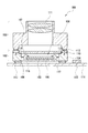
以下、図面を用いて従来の固体撮像カメラモジュールについて説明する。
図6は従来の固体撮像カメラモジュールを説明するための模式的な断面図であり、ここで示す固体撮像カメラモジュール101は、CCD固体撮像装置(半導体パッケージ)102及びレンズ鏡筒103を備える。
Hereinafter, a conventional solid-state imaging camera module will be described with reference to the drawings.
FIG. 6 is a schematic cross-sectional view for explaining a conventional solid-state imaging camera module. The solid-state
上記したCCD固体撮像装置は、半導体パッケージ基台104にダイペースト105でCCD固体撮像素子106が搭載されており、CCD固体撮像素子に形成された第1の端子116と半導体パッケージ基台に形成された第2の端子117とがボンディングワイヤー107により電気的に接続されている。また、半導体パッケージ基台には落とし込み部118が設けられており、この落とし込み部にシール樹脂109を介してシールガラス110を搭載する(配置し固定する)ことによって半導体パッケージ基台の開口部108を閉塞している。
In the CCD solid-state imaging device described above, the CCD solid-
また、レンズ鏡筒は、CCD固体撮像素子上に結像を行なうレンズ111及び赤外光を遮断する光学フィルタ(図示せず)を有し、レンズ固定樹脂112によってCCD固体撮像装置に固定されている。
The lens barrel has a
更に、CCD固体撮像装置は、半導体パッケージ基台の底面に形成された半田バンプ113によってCCD固体撮像素子と他の回路とを電気的に接続するフレキシブル回路基板114に接続されており、このフレキシブル回路基板には回路形成のための電子部品115が実装されている。
Furthermore, the CCD solid-state imaging device is connected to a
ここで、固体撮像装置に対する小型化の要求に対応すべく、半導体パッケージ基台の上面にシールガラスを搭載する構成の固体撮像装置が提案されている(図7(a)参照。)。
即ち、半導体パッケージ基台に落とし込み部を形成し、この落とし込み部にシールガラスを搭載する構成の場合(図6で示す構成の場合)には、落とし込み部の外側領域(図6中符合Aで示す領域)の分だけシールガラスよりも固体撮像装置が大きくなってしまうのに対して、半導体パッケージ基台の上面にシールガラスを搭載する構成の場合(図7(a)で示す構成の場合)には、固体撮像装置は略シールガラスと同じ大きさとすることができ、結果として固体撮像装置の小型化を実現できるために、半導体パッケージ基台の上面にシールガラスを搭載する構成の固体撮像装置が提案されているのである。
Here, in order to meet the demand for downsizing of the solid-state imaging device, a solid-state imaging device having a configuration in which a seal glass is mounted on the upper surface of the semiconductor package base has been proposed (see FIG. 7A).
That is, in the case of a configuration in which a drop portion is formed on the semiconductor package base and a seal glass is mounted on this drop portion (in the case of the configuration shown in FIG. 6), the outer region of the drop portion (indicated by reference numeral A in FIG. 6). In the case where the solid-state imaging device is larger than the seal glass by the area (region), the seal glass is mounted on the upper surface of the semiconductor package base (in the case of the configuration shown in FIG. 7A). The solid-state imaging device can be approximately the same size as the sealing glass, and as a result, the solid-state imaging device can be downsized. It has been proposed.
ところで、近年は、固体撮像装置に対する更なる小型化の要求が強くなってきており、こうした要求に応えるべく、例えば特許文献1で示す様に、ボンディングワイヤーを樹脂材料等の封止体119で封止し、この封止体の上面にシールガラスを搭載する構成の固体撮像装置が提案されている(図7(b)参照。)。
即ち、半導体パッケージ基台の上面にシールガラスを搭載する構成の場合(図7(a)で示す構成の場合)には、半導体パッケージ基台に形成された第2の端子の外側領域(図7(a)中符合Bで示す領域)にシールガラスを支持するための領域を設ける必要があるのに対して、ボンディングワイヤーを封止体で封止し、この封止体の上面にシールガラスを搭載する構成の場合(図7(b)で示す構成の場合)には、第2の端子の外側領域にシールガラスを支持するための領域を設ける必要がなく、結果として固体撮像装置の小型化が実現できるために、ボンディングワイヤーを封止体で封止し、この封止体の上面にシールガラスを搭載する構成の固体撮像装置が提案されているのである。
Incidentally, in recent years, there has been a strong demand for further downsizing of solid-state imaging devices, and in order to meet such demand, for example, as shown in Patent Document 1, a bonding wire is sealed with a sealing
That is, in the case of the configuration in which the seal glass is mounted on the upper surface of the semiconductor package base (in the case of the configuration shown in FIG. 7A), the outer region of the second terminal formed on the semiconductor package base (FIG. 7). It is necessary to provide a region for supporting the seal glass in (a) the region indicated by the middle symbol B), whereas the bonding wire is sealed with a sealing body, and the sealing glass is placed on the upper surface of the sealing body. In the case of the configuration to be mounted (in the case of the configuration shown in FIG. 7B), it is not necessary to provide a region for supporting the seal glass in the outer region of the second terminal, and as a result, the solid-state imaging device is downsized. Therefore, a solid-state imaging device having a configuration in which a bonding wire is sealed with a sealing body and a sealing glass is mounted on the upper surface of the sealing body has been proposed.
しかしながら、上記した固体撮像装置では、樹脂材料等から成る封止体の上面に搭載されたシールガラスの水平度を確保することが困難であった。
即ち、封止体の上面にシールガラスが搭載された固体撮像装置は、樹脂材料等でボンディングワイヤーの封止を行ない、樹脂材料を硬化する前にシールガラスを樹脂材料の上面に配置し、その後に樹脂材料を硬化してシールガラスを固定することによって製造されるのであるが、樹脂材料の上にシールガラスを配置する際に樹脂材料が硬化しておらず、未硬化状態(柔らかい状態)の樹脂材料の上にシールガラスを配置するために、シールガラスの水平度を確保することが困難となるのである。
However, in the solid-state imaging device described above, it has been difficult to ensure the level of the seal glass mounted on the upper surface of the sealing body made of a resin material or the like.
That is, the solid-state imaging device having the sealing glass mounted on the upper surface of the sealing body seals the bonding wire with a resin material or the like, and places the sealing glass on the upper surface of the resin material before curing the resin material. It is manufactured by curing the resin material to fix the seal glass, but when placing the seal glass on the resin material, the resin material is not cured and is in an uncured state (soft state) Since the seal glass is disposed on the resin material, it is difficult to ensure the level of the seal glass.
なお、ボンディングワイヤーを封止した樹脂材料を硬化した後に樹脂材料の上にシールガラスを配置することによって、シールガラスの水平度を確保することは可能である。但し、樹脂材料を硬化した後にシールガラスを樹脂材料の上に配置する場合には、樹脂材料の硬化を待つ必要があり、樹脂材料の硬化に要する時間分だけ歩留りの低下を招くこととなる。更に、硬化した樹脂材料の上に配置したシールガラスを固定するためには、硬化した樹脂材料にシール樹脂を塗布し、あるいはシールガラスにシール樹脂を塗布し、このシール樹脂を介して硬化した樹脂材料の上にシールガラスを配置する必要があり、シール樹脂の塗布作業に起因する余分な工数及び材料を必要とするために、樹脂材料を硬化させ、硬化した樹脂材料の上にシールガラスを搭載するといった方法は必ずしも妥当であるとは言い難い。 In addition, it is possible to ensure the level of the sealing glass by placing the sealing glass on the resin material after curing the resin material sealing the bonding wire. However, when the sealing glass is disposed on the resin material after the resin material is cured, it is necessary to wait for the resin material to be cured, and the yield is reduced by the time required for the resin material to be cured. Furthermore, in order to fix the sealing glass placed on the cured resin material, the sealing resin is applied to the cured resin material, or the sealing resin is applied to the sealing glass, and the resin is cured through the sealing resin. It is necessary to place the seal glass on the material, and in order to require extra man-hours and materials resulting from the application work of the seal resin, the resin material is cured and the seal glass is mounted on the cured resin material It is hard to say that the method of doing is always appropriate.
本発明は、以上の点に鑑みて創案されたものであって、小型化を実現すると共に、シールガラスの水平度の向上を実現することができる固体撮像装置の製造方法を提供することを目的とするものである。 The present invention has been developed in view of the above points, and an object of the present invention is to provide a method for manufacturing a solid-state imaging device capable of realizing downsizing and improving the level of seal glass. It is what.
上記の目的を達成するために、本発明に係る固体撮像装置は、固体撮像素子が搭載された半導体パッケージ基台と、前記固体撮像素子に設けられた第1の端子と前記半導体パッケージ基台に設けられた第2の端子とを電気的に接続するボンディングワイヤーと、少なくとも前記ボンディングワイヤーが接続された前記第2の端子を封止する封止体と、前記固体撮像素子の上方に配置された光透過性材料から成る光透過性部材とを備える固体撮像装置であって、前記光透過性部材は、前記半導体パッケージ基台に形成された一直線上に位置しない3箇所以上の異なる支持部材によって支持されている。 In order to achieve the above object, a solid-state imaging device according to the present invention includes a semiconductor package base on which a solid-state imaging element is mounted, a first terminal provided on the solid-state imaging element, and the semiconductor package base. A bonding wire that electrically connects the provided second terminal, a sealing body that seals at least the second terminal to which the bonding wire is connected, and a solid-state imaging device disposed above A solid-state imaging device including a light transmissive member made of a light transmissive material, wherein the light transmissive member is supported by three or more different support members that are not positioned on a straight line formed on the semiconductor package base. Has been.
ここで、光透過性部材が、半導体パッケージ基台に形成された一直線上に位置しない3箇所以上の異なる支持部材で支持されたことによって、硬化前の封止体のみで光透過性部材を支持する必要がなくなり、封止体を硬化する前に封止体上に光透過性部材を配置したとしても、光透過性部材の水平度を確保することができる。
なお、「半導体パッケージ基台に形成された一直線上に位置しない3箇所以上の異なる支持部材」とは、半導体パッケージ基台と一体的に構成されたものであっても良いし、半導体パッケージ基台とは別体として形成された支持部材を半導体パッケージ基台に取り付けて構成されたものであっても良い。
また、「一直線上に位置しない3箇所以上の異なる支持部材」としたのは、一直線上には配列されず、且つ異なる3箇所以上の点を特定することで平面を特定することができるために、「一直線上に位置しない3箇所以上の異なる支持部材」とすることで光透過性部材が成すべき平面を特定することができるためである。
Here, the light transmitting member is supported by three or more different supporting members that are not positioned on a straight line formed on the semiconductor package base, so that the light transmitting member is supported only by the sealing body before curing. Even if the light transmissive member is disposed on the sealing body before the sealing body is cured, the level of the light transmissive member can be ensured.
The “three or more different support members that are not positioned on a straight line formed on the semiconductor package base” may be configured integrally with the semiconductor package base, or the semiconductor package base. It may be configured by attaching a support member formed separately from the semiconductor package base.
In addition, the reason why “three or more different support members that are not on a straight line” are not arranged on a straight line and because a plane can be specified by specifying three or more different points. This is because it is possible to specify the plane that the light-transmitting member should be formed by using “three or more different support members that are not on a straight line”.
また、封止体により第2の端子のみならず第1の端子をも封止することによって、端子とボンディングワイヤーの接続部における水分の浸入を低減して腐食を抑制することができ、品質向上が実現する。更には、第1の端子、第2の端子及びボンディングワイヤーの全てが封止体により封止されることによって、ボンディングワイヤーそのものの腐食をも抑制することができ、より一層の品質向上が期待できる。 Also, by sealing not only the second terminal but also the first terminal with the sealing body, it is possible to reduce the infiltration of moisture at the connection portion between the terminal and the bonding wire, thereby suppressing corrosion and improving the quality. Is realized. Furthermore, since all of the first terminal, the second terminal, and the bonding wire are sealed with the sealing body, corrosion of the bonding wire itself can be suppressed, and further improvement in quality can be expected. .
また、上記の目的を達成するために、本発明に係る固体撮像装置の製造方法は、固体撮像素子が搭載された半導体パッケージ基台と、前記固体撮像素子に設けられた第1の端子と前記半導体パッケージ基台に設けられた第2の端子とを電気的に接続するボンディングワイヤーと、少なくとも前記ボンディングワイヤーが接続された前記第2の端子を封止する封止体と、前記固体撮像素子の上方に配置された光透過性材料から成る光透過性部材とを備え、前記光透過性部材が、前記半導体パッケージ基台に形成された一直線上に位置しない3箇所以上の異なる支持部材によって支持された固体撮像装置の製造方法であって、前記固体撮像素子を前記半導体パッケージ基台に搭載し、前記第1の端子と前記第2の端子とをボンディングワイヤーによって電気的に接続する工程と、前記ボンディングワイヤーが接続された前記第2の端子を封止体によって封止した後に、前記支持部材及び前記封止体上に前記光透過性部材を配置する工程と、前記封止体を硬化させて前記光透過性部材を固定する工程とを備える。 In order to achieve the above object, a method of manufacturing a solid-state imaging device according to the present invention includes a semiconductor package base on which a solid-state imaging device is mounted, a first terminal provided on the solid-state imaging device, and the A bonding wire that electrically connects the second terminal provided on the semiconductor package base, a sealing body that seals at least the second terminal to which the bonding wire is connected, and a solid-state imaging device A light transmissive member made of a light transmissive material disposed above, and the light transmissive member is supported by three or more different support members that are not positioned on a straight line formed on the semiconductor package base. A method of manufacturing a solid-state imaging device, wherein the solid-state imaging device is mounted on the semiconductor package base, and the first terminal and the second terminal are used as bonding wires. And electrically sealing the second terminal connected to the bonding wire with a sealing body, and then placing the light transmissive member on the support member and the sealing body. And a step of curing the sealing body and fixing the light transmissive member.
また、本発明に係る固体撮像装置の製造方法は、固体撮像素子が搭載された半導体パッケージ基台と、前記固体撮像素子に設けられた第1の端子と前記半導体パッケージ基台に設けられた第2の端子とを電気的に接続するボンディングワイヤーと、少なくとも前記ボンディングワイヤーが接続された前記第2の端子を封止する封止体と、前記固体撮像素子の上方に配置された光透過性材料から成る光透過性部材とを備え、前記光透過性部材が、前記半導体パッケージ基台に形成された一直線上に位置しない3箇所以上の異なる支持部材によって支持された固体撮像装置の製造方法であって、前記固体撮像素子を前記半導体パッケージ基台に搭載し、前記第1の端子と前記第2の端子とをボンディングワイヤーによって電気的に接続する工程と、前記支持部材上にシール材を介して前記光透過性部材を配置して同光透過性部材を固定した後に、前記ボンディングワイヤーが接続された前記第2の端子を封止体によって封止する工程と、前記封止体を硬化させる工程とを備える。 The method for manufacturing a solid-state imaging device according to the present invention includes a semiconductor package base on which a solid-state image sensor is mounted, a first terminal provided on the solid-state image sensor, and a first terminal provided on the semiconductor package base. A bonding wire that electrically connects the two terminals, a sealing body that seals at least the second terminal to which the bonding wire is connected, and a light-transmitting material disposed above the solid-state imaging device And a light-transmitting member comprising: a light-transmitting member, and the light-transmitting member is supported by three or more different supporting members that are not positioned on a straight line formed on the semiconductor package base. Mounting the solid-state imaging device on the semiconductor package base and electrically connecting the first terminal and the second terminal by a bonding wire; A step of sealing the second terminal to which the bonding wire is connected with a sealing body after disposing the light transmissive member on the support member via a sealing material and fixing the light transmissive member. And a step of curing the sealing body.
ここで、半導体パッケージ基台に一直線上に位置しない3箇所以上の異なる支持部材が形成されたことによって、硬化前の封止体のみで光透過性材料を支持する必要がなくなり、封止体を硬化する前に封止体上に光透過性部材を配置したとしても、光透過性部材の水平度を確保することができる。 Here, since the three or more different support members that are not positioned in a straight line are formed on the semiconductor package base, it is not necessary to support the light transmissive material only by the sealing body before curing, Even if the light transmissive member is arranged on the sealing body before curing, the level of the light transmissive member can be ensured.
また、上記の目的を達成するために、本発明に係るカメラモジュールは、固体撮像素子が搭載された半導体パッケージ基台と、前記固体撮像素子に設けられた第1の端子と前記半導体パッケージ基台に設けられた第2の端子とを電気的に接続するボンディングワイヤーと、少なくとも前記ボンディングワイヤーが接続された前記第2の端子を封止する封止体と、前記固体撮像素子の上方に配置された光透過性材料から成る光透過性部材とを有する固体撮像装置と、該固体撮像装置の上方に配置されたレンズと、該レンズを支持する鏡筒部とを備えるカメラモジュールであって、前記光透過性部材は、前記半導体パッケージ基台に形成された一直線上に位置しない3箇所以上の異なる支持部材によって支持されている。 In order to achieve the above object, a camera module according to the present invention includes a semiconductor package base on which a solid-state image sensor is mounted, a first terminal provided on the solid-state image sensor, and the semiconductor package base. A bonding wire that electrically connects the second terminal provided on the substrate, a sealing body that seals at least the second terminal to which the bonding wire is connected, and a solid-state imaging device. A camera module comprising: a solid-state imaging device having a light-transmitting member made of a light-transmitting material; a lens disposed above the solid-state imaging device; and a lens barrel portion that supports the lens, The light transmissive member is supported by three or more different support members that are not positioned on a straight line formed on the semiconductor package base.
ここで、光透過性部材が、半導体パッケージ基台に形成された一直線上に位置しない3箇所以上の異なる支持部材で支持されたことによって、硬化前の封止体で光透過性部材を支持する必要がなくなり、光透過性部材の水平度を確保することができる。 Here, the light transmissive member is supported by three or more different support members that are not positioned on a straight line formed on the semiconductor package base, so that the light transmissive member is supported by the sealing body before curing. This is unnecessary, and the level of the light transmissive member can be ensured.
上記した本発明の固体撮像装置の製造方法では、小型化を実現すると共に、光透過性部材の水平度の向上を図ることができる。 In the above-described method for manufacturing a solid-state imaging device of the present invention, it is possible to reduce the size and improve the level of the light transmissive member.
以下、本発明の実施の形態について図面を参照しながら説明し、本発明の理解に供する。
図1(a)は本発明を適用した固体撮像装置の一例であるCCD固体撮像装置を説明するための模式的な平面図であり、図1(b)は図1(a)中符合X−Xにおける模式的な断面図である。
Hereinafter, embodiments of the present invention will be described with reference to the drawings to facilitate understanding of the present invention.
FIG. 1A is a schematic plan view for explaining a CCD solid-state imaging device which is an example of a solid-state imaging device to which the present invention is applied, and FIG. 1B is a symbol X− in FIG. It is typical sectional drawing in X.
図1示すCCD固体撮像装置1は、セラミック基台2にダイペースト3によってCCD固体撮像素子4が搭載されており、CCD固体撮像素子に形成された第1の端子5とセラミック基台に形成されている第2の端子6とが金細線7により電気的に接続されている。また、セラミック基台の四隅には、後述するシールガラスを支持する支持部材8が形成されている。なお、セラミック基台は半導体パッケージ基台の一例であり、CCD固体撮像素子は固体撮像素子の一例であり、金細線はボンディングワイヤーの一例である。
The CCD solid-state imaging device 1 shown in FIG. 1 has a CCD solid-
また、第2の端子及びこの第2の端子に接続された金細線は、熱硬化性を有するエポキシ樹脂9で封止されており、支持部材及びエポキシ樹脂上にシールガラス10が搭載(配置され固定)されている。ここで、エポキシ樹脂が第2の端子及び金細線を封止するために、第2の端子や金細線の腐食の原因となる化学物質(例えば、ヨウ素や酢酸等)を含まない樹脂を選定する必要がある。なお、エポキシ樹脂は封止体の一例であり、シールガラスは光透過性部材の一例である。
Further, the second terminal and the gold wire connected to the second terminal are sealed with a thermosetting
また、図1に示す固体撮像装置は中空構造であるために、エポキシ樹脂を熱硬化させる際に固体撮像装置の内外の気圧差によって、シールガラスが位置ズレを生じる恐れがある。そこで、セラミック基台にはベントホール11が設けられ、固体撮像装置の内外の気圧差を解消する構造を採っている。更に、CCD固体撮像素子をセラミック基台に搭載する際に塗布するダイペーストによって、ベントホールまでの通気口を塞がないように、セラミック基台の表面にアルミナコート12を施して通気口を確保する構成とされている。 Further, since the solid-state imaging device shown in FIG. 1 has a hollow structure, there is a possibility that the seal glass may be displaced due to a pressure difference between the inside and outside of the solid-state imaging device when the epoxy resin is thermally cured. Therefore, a vent hole 11 is provided in the ceramic base, and a structure for eliminating the pressure difference between the inside and outside of the solid-state imaging device is adopted. Furthermore, with the die paste applied when the CCD solid-state imaging device is mounted on the ceramic base, an alumina coat 12 is applied to the surface of the ceramic base so as not to block the vent to the vent hole, thereby securing the vent. It is supposed to be configured.
ここで、本実施例では、第2の端子及び第2の端子に接続された金細線がエポキシ樹脂で封止された場合、即ち、第2の端子及び金細線の一部がエポキシ樹脂で封止された場合を例に挙げて説明を行っているが、図2で示す様に、第1の端子、第2の端子及び金細線の全部がエポキシ樹脂で封止されても良い。 Here, in this embodiment, when the second terminal and the gold wire connected to the second terminal are sealed with an epoxy resin, that is, the second terminal and a part of the gold wire are sealed with the epoxy resin. Although the case where it is stopped is described as an example, as shown in FIG. 2, all of the first terminal, the second terminal, and the gold wire may be sealed with an epoxy resin.
以下、上記の様に構成されたCCD固体撮像装置の製造方法について説明する。即ち、本発明を適用した固体撮像装置の製造方法について説明する。 Hereinafter, a method for manufacturing the CCD solid-state imaging device configured as described above will be described. That is, a method for manufacturing a solid-state imaging device to which the present invention is applied will be described.
[製造方法(1)](図3(a)参照。)
本発明を適用した固体撮像装置の製造方法の一例では、先ず、ウェーハ上に形成されたCCD固体撮像素子にダイシング処理(ウェーハダイシング)を行なって単個状態のCCD固体撮像素子とした後に(図3(a)中符合a参照。)、単個状態のCCD固体撮像素子4を、複数のセラミック基台が形成されたセラミック基板20(セラミック基台の集合体。図4参照。)の各セラミック基台2の所定領域にダイボンドする(図3(a)中符合b参照。)。
[Production Method (1)] (See FIG. 3A)
In an example of a method for manufacturing a solid-state imaging device to which the present invention is applied, first, a CCD solid-state imaging device formed on a wafer is subjected to a dicing process (wafer dicing) to obtain a single CCD solid-state imaging device (see FIG. 3 (a), reference symbol a).) Each ceramic solid-
次に、CCD固体撮像素子に形成された第1の端子5とセラミック基台に形成された第2の端子6とを金細線7で電気的に接続するワイヤーボンディング処理を行った後に(図3(a)中符合c参照。)、第2の端子及び第2の端子と接続された金細線を被覆する様に熱硬化性のエポキシ樹脂9を塗布する(図3(a)中符合d参照。)。
Next, after performing a wire bonding process for electrically connecting the first terminal 5 formed on the CCD solid-state imaging device and the second terminal 6 formed on the ceramic base with the gold wire 7 (FIG. 3). (A) Refer to the middle symbol c.), A thermosetting
続いて、支持部材上にシールガラス10を配置し(図3(a)中符合e参照。)、加熱処理を行なってエポキシ樹脂(第2の端子及び第2の端子と接続された金細線を被覆する様に塗布されたエポキシ樹脂)を硬化してシールガラスを固定する(図3(a)中符合f参照。)。
Subsequently, the
次に、シールガラスの端部領域に熱硬化性のエポキシ樹脂を塗布し(図3(a)中符合g参照。)、加熱処理を行なってエポキシ樹脂(シールガラスの端部領域に塗布されたエポキシ樹脂)を硬化する(図3(a)中符合h参照。)。 Next, a thermosetting epoxy resin was applied to the end region of the seal glass (see symbol g in FIG. 3A), and heat treatment was performed to apply the epoxy resin (applied to the end region of the seal glass). (Epoxy resin) is cured (see symbol h in FIG. 3A).
なお、シールガラスの端部領域に熱硬化性のエポキシ樹脂を塗布し、熱硬化するのは、固体撮像装置の気密性の向上を図るためであり、シールガラスの端部領域にエポキシ樹脂を塗布しなくても充分な気密性を得ることができるのであれば、シールガラスの端部領域にはエポキシ樹脂を塗布する必要は無い。 In addition, the thermosetting epoxy resin is applied to the end region of the seal glass, and the heat curing is performed in order to improve the airtightness of the solid-state imaging device, and the epoxy resin is applied to the end region of the seal glass. If sufficient hermeticity can be obtained without this, it is not necessary to apply an epoxy resin to the end region of the seal glass.
その後、図4中符号Xで示すダイシングラインをダイシングすることによってセラミック基板を個片化して固体撮像装置を得ることができる(図3(a)中符合i参照。)。なお、こうして得られた固体撮像装置は画質検査を経て出荷されることとなる(図3(a)中符合j参照。)。 Thereafter, the ceramic substrate is separated into pieces by dicing a dicing line indicated by a symbol X in FIG. 4 to obtain a solid-state imaging device (see symbol i in FIG. 3A). Note that the solid-state imaging device thus obtained is shipped after an image quality inspection (see reference numeral j in FIG. 3A).
[製造方法(2)](図3(b)参照。)
本発明を適用した固体撮像装置の製造方法の他の一例では、上記した製造方法(1)と同様に、先ず、ウェーハ上に形成されたCCD固体撮像素子にダイシング処理(ウェーハダイシング)を行なって単個状態のCCD固体撮像素子とした後に(図3(b)中符合a参照。)、単個状態のCCD固体撮像素子を、複数のセラミック基台が形成されたセラミック基板(セラミック基台の集合体)の各セラミック基台の所定領域にダイボンドする(図3(b)中符合b参照。)。
[Manufacturing method (2)] (Refer to Drawing 3 (b).)
In another example of the manufacturing method of the solid-state imaging device to which the present invention is applied, the CCD solid-state imaging device formed on the wafer is first subjected to dicing processing (wafer dicing) as in the manufacturing method (1) described above. After the CCD solid-state imaging device in a single state (see symbol a in FIG. 3B), the CCD solid-state imaging device in a single state is placed on a ceramic substrate (a ceramic base of a ceramic base). Die-bonded to a predetermined region of each ceramic base of the aggregate (see symbol b in FIG. 3B).
次に、CCD固体撮像素子に形成された第1の端子とセラミック基台に形成された第2の端子とを金細線で電気的に接続するワイヤーボンディング処理を行なう(図3(b)中符合c参照。)。 Next, a wire bonding process is performed in which the first terminal formed on the CCD solid-state image pickup device and the second terminal formed on the ceramic base are electrically connected by a thin gold wire (reference numeral in FIG. 3B). c).
続いて、支持部材表面にシール樹脂(図1には図示せず)を塗布し(図3(b)中符合d参照。)、このシール樹脂を介してシールガラスを配置し固定する(図3(b)中符合e参照。)。なお、上記した製造方法(1)では支持部材表面にシール樹脂を塗布することなくシールガラスを支持部材上に配置していたために、樹脂材料を硬化するまでシールガラスが固定されることはないが、ここでは、支持部材表面にシール樹脂を塗布した状態でシールガラスを支持部材上に配置するので、シールガラスは支持部材上に固定されることとなる。 Subsequently, a sealing resin (not shown in FIG. 1) is applied to the surface of the support member (see reference numeral d in FIG. 3B), and the sealing glass is disposed and fixed via the sealing resin (FIG. 3). (B) Refer to the middle sign e.). In the manufacturing method (1) described above, since the sealing glass is disposed on the supporting member without applying the sealing resin to the surface of the supporting member, the sealing glass is not fixed until the resin material is cured. Here, since the sealing glass is disposed on the supporting member in a state where the sealing resin is applied to the surface of the supporting member, the sealing glass is fixed on the supporting member.
また、第2の端子及び第2の端子と接続された金細線を被覆する様に熱硬化性のエポキシ樹脂を塗布すると共に、シールガラスの端部領域に熱硬化性のエポキシ樹脂を塗布した後に(図3(b)中符合f参照。)、加熱処理を行なってエポキシ樹脂(第2の端子及び第2の端子と接続された金細線を被覆する様に塗布されたエポキシ樹脂及びシールガラスの端部領域に塗布されたエポキシ樹脂)を硬化する(図3(b)中符合g参照。)。 In addition, after applying a thermosetting epoxy resin so as to cover the second terminal and the gold wire connected to the second terminal, and after applying the thermosetting epoxy resin to the end region of the seal glass (See symbol f in FIG. 3B.) An epoxy resin (sealed glass and epoxy resin applied so as to cover the second terminals and the gold wires connected to the second terminals) by heat treatment. The epoxy resin applied to the end region is cured (see reference numeral g in FIG. 3B).
なお、上記した製造方法(1)と同様に、シールガラスの端部領域に熱硬化性のエポキシ樹脂を塗布し、熱硬化するのは、固体撮像装置の気密性の向上を図るためであり、シールガラスの端部領域にエポキシ樹脂を塗布しなくても充分な気密性を得ることができるのであれば、シールガラスの端部領域にはエポキシ樹脂を塗布する必要は無い。 In addition, as with the manufacturing method (1) described above, the thermosetting epoxy resin is applied to the end region of the seal glass and is thermally cured in order to improve the airtightness of the solid-state imaging device. If sufficient airtightness can be obtained without applying an epoxy resin to the end region of the seal glass, it is not necessary to apply an epoxy resin to the end region of the seal glass.
その後、ダイシング処理によってセラミック基板を個片化して固体撮像装置を得ることができる(図3(b)中符合h参照。)。なお、こうして得られた固体撮像装置は画質検査を経て出荷されることとなる(図3(b)中符合i参照。)。 After that, the solid-state imaging device can be obtained by dividing the ceramic substrate into pieces by a dicing process (see symbol h in FIG. 3B). Note that the solid-state imaging device thus obtained is shipped after an image quality inspection (see reference numeral i in FIG. 3B).
本発明を適用した固体撮像装置では、セラミック基台に設けられた支持部材によってシールガラスが支持されているために、エポキシ樹脂上に搭載されたシールガラスの水平度を確保することが可能となる。
即ち、未硬化状態のエポキシ樹脂上にシールガラスを配置したとしても、支持部材がシールガラスを支持するためにシールガラスの水平度を確保することが可能となる。
In the solid-state imaging device to which the present invention is applied, since the seal glass is supported by the support member provided on the ceramic base, it is possible to ensure the level of the seal glass mounted on the epoxy resin. .
That is, even when the seal glass is disposed on the uncured epoxy resin, the support member supports the seal glass, so that the level of the seal glass can be ensured.
具体的には、固体撮像装置の製造方法(1)において、第2の端子及び第2の端子と接続された金細線を被覆する様に熱硬化性のエポキシ樹脂を塗布し(図3(a)中符合d参照。)、エポキシ樹脂の上にシールガラスを配置し(図3(a)中符合e参照。)、エポキシ樹脂を熱硬化する(図3(a)中符合f参照。)ことによってシールガラスを固定しているのであるが、支持部材が設けられていない場合には、エポキシ樹脂上に配置されたシールガラスを未硬化のエポキシ樹脂で支持しなければならず、未硬化状態のエポキシ樹脂上にシールガラスを配置することに起因してシールガラスの水平度の低下が懸念される。これに対して、セラミック基台に支持部材が設けられた本実施例の場合には、エポキシ樹脂上に配置されたシールガラスは支持部材で支持されることとなり、エポキシ樹脂が未硬化だったとしてもシールガラスの水平度は支持部材によって確保されることとなるのである。 Specifically, in the manufacturing method (1) of the solid-state imaging device, a thermosetting epoxy resin is applied so as to cover the second terminal and the gold wire connected to the second terminal (FIG. 3A ) Refer to the middle symbol d.), Arrange the seal glass on the epoxy resin (see the symbol e in FIG. 3A), and heat cure the epoxy resin (see the symbol f in FIG. 3A). If the support glass is not provided, the seal glass placed on the epoxy resin must be supported by the uncured epoxy resin. Due to the arrangement of the seal glass on the epoxy resin, there is a concern that the level of the seal glass is lowered. On the other hand, in the case of the present embodiment in which the support member is provided on the ceramic base, the seal glass disposed on the epoxy resin is supported by the support member, and the epoxy resin is uncured. In addition, the level of the sealing glass is secured by the support member.
また、本発明を適用した固体撮像装置では、シールガラスの四隅を支持しているために、シールガラスの四辺を支持する固体撮像装置と比べるとシールガラスの水平度を確保することができる。
以下、この点について図5を参照して説明を行う。
Moreover, in the solid-state imaging device to which the present invention is applied, since the four corners of the seal glass are supported, the level of the seal glass can be ensured as compared with the solid-state imaging device that supports the four sides of the seal glass.
Hereinafter, this point will be described with reference to FIG.
即ち、従来の固体撮像装置の様に、シールガラスの四辺を支持する構成の場合には、シールガラスの支持面に変形等に起因した意図しない突起物13が生じた場合に、この突起物が原因となって、シールガラスの一方の辺(図5(a)中符合C側の辺)をセラミック基台で支持しようとすると、シールガラスの他方の辺(図5(a)中符合D側の辺)は突起物の高さ以上の位置ズレを生じることとなる。具体的には、突起物の高さ(図5中符合Tで示す高さ)以上の高さの位置ズレ(図5中符合Sで示す高さの位置ズレ)が生じる。
これに対して、シールガラスの四隅を支持する本実施例の固体撮像装置の場合には、支持部材表面に変形等に起因した意図しない突起物が生じたとしても、この突起物が原因でのシールガラスの位置ズレは突起物の高さ(図5中符合Tで示す高さ)に抑えることができるため(図5(b)参照。)、シールガラスの四隅を支持することによって、上記した様に四辺を支持する固体撮像装置と比べるとシールガラスの水平度を確保することができるのである。
That is, in the case of a configuration that supports the four sides of the seal glass as in a conventional solid-state imaging device, when an
On the other hand, in the case of the solid-state imaging device of the present embodiment that supports the four corners of the seal glass, even if an unintended protrusion due to deformation or the like occurs on the surface of the support member, Since the positional deviation of the seal glass can be suppressed to the height of the protrusion (the height indicated by the symbol T in FIG. 5) (see FIG. 5B), the above-described difference is achieved by supporting the four corners of the seal glass. Thus, the level of the sealing glass can be ensured as compared with the solid-state imaging device that supports the four sides.
また、本発明を適用した固体撮像装置は、セラミック基台にベントホールが形成されているために、エポキシ樹脂を熱硬化させる際の密閉空間の温度気圧差によるシールガラスの位置ズレを抑制することができる。 In addition, since the solid-state imaging device to which the present invention is applied has a vent hole formed in the ceramic base, it suppresses the positional deviation of the seal glass due to the temperature and pressure difference in the sealed space when the epoxy resin is thermally cured. Can do.
また、本発明を適用した固体撮像装置は、上記の様に、シールガラスの水平度を確保することができると共に、シールガラスの位置ズレを抑制することができるために、固体撮像装置の表面形状がもたらす光学的影響についても改善が期待できる。 In addition, the solid-state imaging device to which the present invention is applied can ensure the level of the seal glass as described above, and can suppress the positional deviation of the seal glass. Improvements can also be expected for the optical effects caused by.
また、本発明を適用した固体撮像装置の製造方法の一例(製造方法(1))は、シールガラスを支持部材に固定するためのシール樹脂を使用することなく、封止を目的としたエポキシ樹脂の接着力を利用してエポキシ樹脂上にシールガラスを固定しており、シールガラスの固定及びエポキシ樹脂による封止を単一の樹脂材料で行なうことが可能である。 An example of a method for manufacturing a solid-state imaging device to which the present invention is applied (manufacturing method (1)) is an epoxy resin for sealing purposes without using a sealing resin for fixing a sealing glass to a support member. The sealing glass is fixed on the epoxy resin by using the adhesive force of the above, and the sealing glass can be fixed and sealed with the epoxy resin with a single resin material.
また、本発明を適用した固体撮像装置の製造方法の他の一例(製造方法(2))は、シール樹脂を用いてシールガラスを支持部材に固定した後に、セラミック基台とシールガラスの間隙にエポキシ樹脂を充填して封止しており、シールガラスを固定した後にエポキシ樹脂を充填(塗布)していることから、高い精度でシールガラスを搭載することが可能である。 Another example of the manufacturing method of the solid-state imaging device to which the present invention is applied (manufacturing method (2)) is that the sealing glass is fixed to the support member using the sealing resin, and then the gap between the ceramic base and the sealing glass Since the epoxy resin is filled and sealed, and the sealing glass is fixed and then filled (coated), the sealing glass can be mounted with high accuracy.
1 CCD固体撮像装置
2 セラミック基台
3 ダイペースト
4 CCD固体撮像素子
5 第1の端子
6 第2の端子
7 金細線
8 支持部材
9 エポキシ樹脂
10 シールガラス
11 ベントホール
12 アルミナコート
13 突起物
20 セラミック基板
DESCRIPTION OF SYMBOLS 1 CCD solid-
Claims (1)
前記固体撮像素子を前記半導体パッケージ基台に搭載し、前記第1の端子と前記第2の端子とをボンディングワイヤーによって電気的に接続する工程と、Mounting the solid-state imaging device on the semiconductor package base and electrically connecting the first terminal and the second terminal by a bonding wire;
前記支持部材上にシール材を介して前記光透過性部材を配置して同光透過性部材を固定した後に、前記ボンディングワイヤーが接続された前記第2の端子を封止体によって封止する工程と、A step of sealing the second terminal to which the bonding wire is connected with a sealing body after disposing the light transmissive member on the support member via a sealing material and fixing the light transmissive member. When,
前記封止体を硬化させる工程とを備えるCuring the sealing body.
固体撮像装置の製造方法。Manufacturing method of solid-state imaging device.
Priority Applications (5)
| Application Number | Priority Date | Filing Date | Title |
|---|---|---|---|
| JP2005356354A JP4466552B2 (en) | 2005-12-09 | 2005-12-09 | Method for manufacturing solid-state imaging device |
| US11/567,959 US20070194439A1 (en) | 2005-12-09 | 2006-12-07 | Solid-state imaging device, fabrication method of the same, and camera module |
| KR1020060124217A KR101283217B1 (en) | 2005-12-09 | 2006-12-08 | Solid state imaging device and manufacturing method thereof, and camera module |
| CN2006100647587A CN1979882B (en) | 2005-12-09 | 2006-12-11 | Solid-state imaging device, fabrication method of the same, and camera module |
| US12/555,664 US8952412B2 (en) | 2005-12-09 | 2009-09-08 | Method for fabricating a solid-state imaging package |
Applications Claiming Priority (1)
| Application Number | Priority Date | Filing Date | Title |
|---|---|---|---|
| JP2005356354A JP4466552B2 (en) | 2005-12-09 | 2005-12-09 | Method for manufacturing solid-state imaging device |
Publications (2)
| Publication Number | Publication Date |
|---|---|
| JP2007165386A JP2007165386A (en) | 2007-06-28 |
| JP4466552B2 true JP4466552B2 (en) | 2010-05-26 |
Family
ID=38130971
Family Applications (1)
| Application Number | Title | Priority Date | Filing Date |
|---|---|---|---|
| JP2005356354A Expired - Fee Related JP4466552B2 (en) | 2005-12-09 | 2005-12-09 | Method for manufacturing solid-state imaging device |
Country Status (4)
| Country | Link |
|---|---|
| US (2) | US20070194439A1 (en) |
| JP (1) | JP4466552B2 (en) |
| KR (1) | KR101283217B1 (en) |
| CN (1) | CN1979882B (en) |
Families Citing this family (9)
| Publication number | Priority date | Publication date | Assignee | Title |
|---|---|---|---|---|
| JP2007012895A (en) * | 2005-06-30 | 2007-01-18 | Sanyo Electric Co Ltd | Circuit device and manufacturing method thereof |
| US9275949B2 (en) * | 2011-06-01 | 2016-03-01 | Canon Kabushiki Kaisha | Semiconductor device |
| JP2013211695A (en) * | 2012-03-30 | 2013-10-10 | Konica Minolta Inc | Imaging apparatus |
| US9826131B2 (en) | 2013-09-23 | 2017-11-21 | Heptagon Micro Optics Pte. Ltd. | Compact camera module arrangements that facilitate dam-and-fill and similar encapsulation techniques |
| US10750060B2 (en) * | 2016-03-31 | 2020-08-18 | Sony Corporation | Camera module, method of manufacturing camera module, imaging apparatus, and electronic apparatus |
| JP7414720B2 (en) * | 2018-08-21 | 2024-01-16 | ソニーセミコンダクタソリューションズ株式会社 | Semiconductor device, electronic device, and method for manufacturing semiconductor device |
| US11037970B2 (en) * | 2018-11-01 | 2021-06-15 | Semiconductor Components Industries, Llc | Semiconductor package structure and related methods |
| JP6839248B1 (en) * | 2019-09-30 | 2021-03-03 | 浜松ホトニクス株式会社 | Photodetector |
| CN117766551A (en) * | 2022-09-16 | 2024-03-26 | 星科金朋私人有限公司 | Sensor assembly and method of forming the same |
Family Cites Families (17)
| Publication number | Priority date | Publication date | Assignee | Title |
|---|---|---|---|---|
| KR970003915B1 (en) * | 1987-06-24 | 1997-03-22 | 미다 가쓰시게 | Semiconductor memory device and semiconductor memory module using same |
| US5721450A (en) * | 1995-06-12 | 1998-02-24 | Motorola, Inc. | Moisture relief for chip carriers |
| JP3880278B2 (en) * | 2000-03-10 | 2007-02-14 | オリンパス株式会社 | Solid-state imaging device and manufacturing method thereof |
| US6759743B2 (en) * | 2000-09-11 | 2004-07-06 | Xytrans, Inc. | Thick film millimeter wave transceiver module |
| TW471143B (en) * | 2001-01-04 | 2002-01-01 | Wen-Wen Chiou | Integrated circuit chip package |
| TW473951B (en) * | 2001-01-17 | 2002-01-21 | Siliconware Precision Industries Co Ltd | Non-leaded quad flat image sensor package |
| JP2003133562A (en) * | 2001-10-19 | 2003-05-09 | Kyocera Corp | Optical semiconductor device |
| JP2003332542A (en) * | 2002-05-09 | 2003-11-21 | Shinko Electric Ind Co Ltd | Semiconductor device and method of manufacturing the same |
| JP2004146609A (en) | 2002-10-24 | 2004-05-20 | Kyocera Corp | Optical semiconductor device |
| US6982470B2 (en) * | 2002-11-27 | 2006-01-03 | Seiko Epson Corporation | Semiconductor device, method of manufacturing the same, cover for semiconductor device, and electronic equipment |
| JP2005183923A (en) * | 2003-11-28 | 2005-07-07 | Matsushita Electric Ind Co Ltd | Semiconductor device and manufacturing method thereof |
| JP4409338B2 (en) | 2004-03-31 | 2010-02-03 | パナソニック株式会社 | Solid-state imaging device and manufacturing method thereof |
| US20050236644A1 (en) * | 2004-04-27 | 2005-10-27 | Greg Getten | Sensor packages and methods of making the same |
| JP2006278726A (en) * | 2005-03-29 | 2006-10-12 | Sharp Corp | Semiconductor device module and manufacturing method of semiconductor device module |
| JP4827593B2 (en) | 2005-07-19 | 2011-11-30 | パナソニック株式会社 | Semiconductor device and manufacturing method thereof |
| US20070120213A1 (en) * | 2005-11-28 | 2007-05-31 | Hiew Siew S | Wire under dam package and method for packaging image-sensor |
| US20080099866A1 (en) * | 2006-10-25 | 2008-05-01 | Impac Technology Co., Ltd. | Image sensing module and method for packaging the same |
-
2005
- 2005-12-09 JP JP2005356354A patent/JP4466552B2/en not_active Expired - Fee Related
-
2006
- 2006-12-07 US US11/567,959 patent/US20070194439A1/en not_active Abandoned
- 2006-12-08 KR KR1020060124217A patent/KR101283217B1/en not_active Expired - Fee Related
- 2006-12-11 CN CN2006100647587A patent/CN1979882B/en not_active Expired - Fee Related
-
2009
- 2009-09-08 US US12/555,664 patent/US8952412B2/en active Active
Also Published As
| Publication number | Publication date |
|---|---|
| US20070194439A1 (en) | 2007-08-23 |
| US20100009490A1 (en) | 2010-01-14 |
| US8952412B2 (en) | 2015-02-10 |
| CN1979882A (en) | 2007-06-13 |
| JP2007165386A (en) | 2007-06-28 |
| KR20070061423A (en) | 2007-06-13 |
| KR101283217B1 (en) | 2013-07-05 |
| CN1979882B (en) | 2011-09-14 |
Similar Documents
| Publication | Publication Date | Title |
|---|---|---|
| KR100604190B1 (en) | Solid state imaging device, semiconductor wafer, optical device module, method of solid state imaging device fabrication, and method of optical device module fabrication | |
| US7964945B2 (en) | Glass cap molding package, manufacturing method thereof and camera module | |
| KR100658150B1 (en) | Camera module and its manufacturing method | |
| JP5746919B2 (en) | Semiconductor package | |
| CN101310381B (en) | Semiconductor package and manufacturing method thereof, semiconductor module and electronic device | |
| US20070241273A1 (en) | Camera module | |
| US8952412B2 (en) | Method for fabricating a solid-state imaging package | |
| JP4673721B2 (en) | Imaging apparatus and manufacturing method thereof | |
| US11417693B2 (en) | Module, method for manufacturing module, and electronic device | |
| JP2011165774A (en) | Production method of solid-state image pickup device | |
| JP6221299B2 (en) | Hermetic sealing body and hermetic sealing method | |
| KR20120106018A (en) | Camera module and the fabricating method thereof | |
| JP2009044494A (en) | Imaging device | |
| JP2006269841A (en) | Solid-state imaging device | |
| JP5162607B2 (en) | Assembling the camera module | |
| JP4806970B2 (en) | Solid-state imaging device | |
| US20090315130A1 (en) | Solid-state imaging apparatus and method for manufacturing the same | |
| KR100917026B1 (en) | Glass cap molding package and manufacturing method thereof, and camera module | |
| JP4578168B2 (en) | Method for manufacturing solid-state imaging device | |
| US20240387588A1 (en) | Image sensor packages and method thereof | |
| JP2014103170A (en) | Image pickup device, method for manufacturing the same, and camera | |
| JP2006269784A (en) | Imaging apparatus | |
| KR100840153B1 (en) | Camera module | |
| KR100927423B1 (en) | Glass cap molding package and manufacturing method thereof, and camera module | |
| JP2008166939A (en) | The camera module |
Legal Events
| Date | Code | Title | Description |
|---|---|---|---|
| A131 | Notification of reasons for refusal |
Free format text: JAPANESE INTERMEDIATE CODE: A131 Effective date: 20091124 |
|
| A977 | Report on retrieval |
Free format text: JAPANESE INTERMEDIATE CODE: A971007 Effective date: 20091126 |
|
| A521 | Request for written amendment filed |
Free format text: JAPANESE INTERMEDIATE CODE: A523 Effective date: 20100104 |
|
| TRDD | Decision of grant or rejection written | ||
| A01 | Written decision to grant a patent or to grant a registration (utility model) |
Free format text: JAPANESE INTERMEDIATE CODE: A01 Effective date: 20100202 |
|
| A01 | Written decision to grant a patent or to grant a registration (utility model) |
Free format text: JAPANESE INTERMEDIATE CODE: A01 |
|
| A61 | First payment of annual fees (during grant procedure) |
Free format text: JAPANESE INTERMEDIATE CODE: A61 Effective date: 20100215 |
|
| FPAY | Renewal fee payment (event date is renewal date of database) |
Free format text: PAYMENT UNTIL: 20130305 Year of fee payment: 3 |
|
| FPAY | Renewal fee payment (event date is renewal date of database) |
Free format text: PAYMENT UNTIL: 20130305 Year of fee payment: 3 |
|
| FPAY | Renewal fee payment (event date is renewal date of database) |
Free format text: PAYMENT UNTIL: 20140305 Year of fee payment: 4 |
|
| R250 | Receipt of annual fees |
Free format text: JAPANESE INTERMEDIATE CODE: R250 |
|
| LAPS | Cancellation because of no payment of annual fees |