JP4925832B2 - Method for mounting an optical sensor - Google Patents
Method for mounting an optical sensor Download PDFInfo
- Publication number
- JP4925832B2 JP4925832B2 JP2006549338A JP2006549338A JP4925832B2 JP 4925832 B2 JP4925832 B2 JP 4925832B2 JP 2006549338 A JP2006549338 A JP 2006549338A JP 2006549338 A JP2006549338 A JP 2006549338A JP 4925832 B2 JP4925832 B2 JP 4925832B2
- Authority
- JP
- Japan
- Prior art keywords
- lead frame
- leadframe
- panel
- lens
- lead
- Prior art date
- Legal status (The legal status is an assumption and is not a legal conclusion. Google has not performed a legal analysis and makes no representation as to the accuracy of the status listed.)
- Expired - Fee Related
Links
- 230000003287 optical effect Effects 0.000 title claims description 28
- 238000000034 method Methods 0.000 title claims description 27
- 239000000853 adhesive Substances 0.000 claims description 17
- 230000001070 adhesive effect Effects 0.000 claims description 17
- 150000001875 compounds Chemical class 0.000 claims description 11
- 238000000465 moulding Methods 0.000 claims description 10
- 230000002093 peripheral effect Effects 0.000 claims description 10
- RYGMFSIKBFXOCR-UHFFFAOYSA-N Copper Chemical compound [Cu] RYGMFSIKBFXOCR-UHFFFAOYSA-N 0.000 claims description 5
- 229910052802 copper Inorganic materials 0.000 claims description 5
- 239000010949 copper Substances 0.000 claims description 5
- 239000011521 glass Substances 0.000 claims description 5
- 239000011347 resin Substances 0.000 claims description 5
- 229920005989 resin Polymers 0.000 claims description 5
- 238000003825 pressing Methods 0.000 claims description 4
- 238000000926 separation method Methods 0.000 claims description 4
- 230000000740 bleeding effect Effects 0.000 claims description 3
- 239000004593 Epoxy Substances 0.000 claims description 2
- 239000002184 metal Substances 0.000 description 5
- 229910052751 metal Inorganic materials 0.000 description 5
- 238000004519 manufacturing process Methods 0.000 description 4
- JQUCWIWWWKZNCS-LESHARBVSA-N C(C1=CC=CC=C1)(=O)NC=1SC[C@H]2[C@@](N1)(CO[C@H](C2)C)C=2SC=C(N2)NC(=O)C2=NC=C(C=C2)OC(F)F Chemical compound C(C1=CC=CC=C1)(=O)NC=1SC[C@H]2[C@@](N1)(CO[C@H](C2)C)C=2SC=C(N2)NC(=O)C2=NC=C(C=C2)OC(F)F JQUCWIWWWKZNCS-LESHARBVSA-N 0.000 description 3
- 239000011159 matrix material Substances 0.000 description 3
- 238000004140 cleaning Methods 0.000 description 2
- 238000005530 etching Methods 0.000 description 2
- PCHJSUWPFVWCPO-UHFFFAOYSA-N gold Chemical compound [Au] PCHJSUWPFVWCPO-UHFFFAOYSA-N 0.000 description 2
- 229910052737 gold Inorganic materials 0.000 description 2
- 239000010931 gold Substances 0.000 description 2
- 239000000463 material Substances 0.000 description 2
- 229920003023 plastic Polymers 0.000 description 2
- 239000000919 ceramic Substances 0.000 description 1
- 238000007796 conventional method Methods 0.000 description 1
- 230000007547 defect Effects 0.000 description 1
- 238000002347 injection Methods 0.000 description 1
- 239000007924 injection Substances 0.000 description 1
- 238000001746 injection moulding Methods 0.000 description 1
- 238000009434 installation Methods 0.000 description 1
- 239000007788 liquid Substances 0.000 description 1
- 150000002739 metals Chemical class 0.000 description 1
- 238000012986 modification Methods 0.000 description 1
- 230000004048 modification Effects 0.000 description 1
- 238000012858 packaging process Methods 0.000 description 1
- 238000004080 punching Methods 0.000 description 1
- 239000004065 semiconductor Substances 0.000 description 1
- 239000000758 substrate Substances 0.000 description 1
- 229920001187 thermosetting polymer Polymers 0.000 description 1
- XLYOFNOQVPJJNP-UHFFFAOYSA-N water Substances O XLYOFNOQVPJJNP-UHFFFAOYSA-N 0.000 description 1
Images


Classifications
-
- H—ELECTRICITY
- H01—ELECTRIC ELEMENTS
- H01L—SEMICONDUCTOR DEVICES NOT COVERED BY CLASS H10
- H01L31/00—Semiconductor devices sensitive to infrared radiation, light, electromagnetic radiation of shorter wavelength or corpuscular radiation and specially adapted either for the conversion of the energy of such radiation into electrical energy or for the control of electrical energy by such radiation; Processes or apparatus specially adapted for the manufacture or treatment thereof or of parts thereof; Details thereof
- H01L31/02—Details
- H01L31/0203—Containers; Encapsulations, e.g. encapsulation of photodiodes
-
- H—ELECTRICITY
- H01—ELECTRIC ELEMENTS
- H01L—SEMICONDUCTOR DEVICES NOT COVERED BY CLASS H10
- H01L23/00—Details of semiconductor or other solid state devices
- H01L23/02—Containers; Seals
- H01L23/04—Containers; Seals characterised by the shape of the container or parts, e.g. caps, walls
- H01L23/053—Containers; Seals characterised by the shape of the container or parts, e.g. caps, walls the container being a hollow construction and having an insulating or insulated base as a mounting for the semiconductor body
-
- H—ELECTRICITY
- H01—ELECTRIC ELEMENTS
- H01L—SEMICONDUCTOR DEVICES NOT COVERED BY CLASS H10
- H01L23/00—Details of semiconductor or other solid state devices
- H01L23/02—Containers; Seals
-
- H—ELECTRICITY
- H01—ELECTRIC ELEMENTS
- H01L—SEMICONDUCTOR DEVICES NOT COVERED BY CLASS H10
- H01L23/00—Details of semiconductor or other solid state devices
- H01L23/48—Arrangements for conducting electric current to or from the solid state body in operation, e.g. leads, terminal arrangements ; Selection of materials therefor
- H01L23/488—Arrangements for conducting electric current to or from the solid state body in operation, e.g. leads, terminal arrangements ; Selection of materials therefor consisting of soldered or bonded constructions
- H01L23/495—Lead-frames or other flat leads
-
- H—ELECTRICITY
- H01—ELECTRIC ELEMENTS
- H01L—SEMICONDUCTOR DEVICES NOT COVERED BY CLASS H10
- H01L24/00—Arrangements for connecting or disconnecting semiconductor or solid-state bodies; Methods or apparatus related thereto
- H01L24/93—Batch processes
- H01L24/95—Batch processes at chip-level, i.e. with connecting carried out on a plurality of singulated devices, i.e. on diced chips
- H01L24/97—Batch processes at chip-level, i.e. with connecting carried out on a plurality of singulated devices, i.e. on diced chips the devices being connected to a common substrate, e.g. interposer, said common substrate being separable into individual assemblies after connecting
-
- H—ELECTRICITY
- H01—ELECTRIC ELEMENTS
- H01L—SEMICONDUCTOR DEVICES NOT COVERED BY CLASS H10
- H01L27/00—Devices consisting of a plurality of semiconductor or other solid-state components formed in or on a common substrate
- H01L27/14—Devices consisting of a plurality of semiconductor or other solid-state components formed in or on a common substrate including semiconductor components sensitive to infrared radiation, light, electromagnetic radiation of shorter wavelength or corpuscular radiation and specially adapted either for the conversion of the energy of such radiation into electrical energy or for the control of electrical energy by such radiation
- H01L27/144—Devices controlled by radiation
- H01L27/146—Imager structures
- H01L27/14601—Structural or functional details thereof
- H01L27/14618—Containers
-
- H—ELECTRICITY
- H01—ELECTRIC ELEMENTS
- H01L—SEMICONDUCTOR DEVICES NOT COVERED BY CLASS H10
- H01L27/00—Devices consisting of a plurality of semiconductor or other solid-state components formed in or on a common substrate
- H01L27/14—Devices consisting of a plurality of semiconductor or other solid-state components formed in or on a common substrate including semiconductor components sensitive to infrared radiation, light, electromagnetic radiation of shorter wavelength or corpuscular radiation and specially adapted either for the conversion of the energy of such radiation into electrical energy or for the control of electrical energy by such radiation
- H01L27/144—Devices controlled by radiation
- H01L27/146—Imager structures
- H01L27/14683—Processes or apparatus peculiar to the manufacture or treatment of these devices or parts thereof
-
- H—ELECTRICITY
- H01—ELECTRIC ELEMENTS
- H01L—SEMICONDUCTOR DEVICES NOT COVERED BY CLASS H10
- H01L2224/00—Indexing scheme for arrangements for connecting or disconnecting semiconductor or solid-state bodies and methods related thereto as covered by H01L24/00
- H01L2224/01—Means for bonding being attached to, or being formed on, the surface to be connected, e.g. chip-to-package, die-attach, "first-level" interconnects; Manufacturing methods related thereto
- H01L2224/42—Wire connectors; Manufacturing methods related thereto
- H01L2224/47—Structure, shape, material or disposition of the wire connectors after the connecting process
- H01L2224/48—Structure, shape, material or disposition of the wire connectors after the connecting process of an individual wire connector
- H01L2224/4805—Shape
- H01L2224/4809—Loop shape
- H01L2224/48091—Arched
-
- H—ELECTRICITY
- H01—ELECTRIC ELEMENTS
- H01L—SEMICONDUCTOR DEVICES NOT COVERED BY CLASS H10
- H01L2224/00—Indexing scheme for arrangements for connecting or disconnecting semiconductor or solid-state bodies and methods related thereto as covered by H01L24/00
- H01L2224/01—Means for bonding being attached to, or being formed on, the surface to be connected, e.g. chip-to-package, die-attach, "first-level" interconnects; Manufacturing methods related thereto
- H01L2224/42—Wire connectors; Manufacturing methods related thereto
- H01L2224/47—Structure, shape, material or disposition of the wire connectors after the connecting process
- H01L2224/48—Structure, shape, material or disposition of the wire connectors after the connecting process of an individual wire connector
- H01L2224/481—Disposition
- H01L2224/48151—Connecting between a semiconductor or solid-state body and an item not being a semiconductor or solid-state body, e.g. chip-to-substrate, chip-to-passive
- H01L2224/48221—Connecting between a semiconductor or solid-state body and an item not being a semiconductor or solid-state body, e.g. chip-to-substrate, chip-to-passive the body and the item being stacked
- H01L2224/48225—Connecting between a semiconductor or solid-state body and an item not being a semiconductor or solid-state body, e.g. chip-to-substrate, chip-to-passive the body and the item being stacked the item being non-metallic, e.g. insulating substrate with or without metallisation
- H01L2224/48227—Connecting between a semiconductor or solid-state body and an item not being a semiconductor or solid-state body, e.g. chip-to-substrate, chip-to-passive the body and the item being stacked the item being non-metallic, e.g. insulating substrate with or without metallisation connecting the wire to a bond pad of the item
-
- H—ELECTRICITY
- H01—ELECTRIC ELEMENTS
- H01L—SEMICONDUCTOR DEVICES NOT COVERED BY CLASS H10
- H01L2924/00—Indexing scheme for arrangements or methods for connecting or disconnecting semiconductor or solid-state bodies as covered by H01L24/00
- H01L2924/10—Details of semiconductor or other solid state devices to be connected
- H01L2924/11—Device type
- H01L2924/14—Integrated circuits
-
- H—ELECTRICITY
- H01—ELECTRIC ELEMENTS
- H01L—SEMICONDUCTOR DEVICES NOT COVERED BY CLASS H10
- H01L2924/00—Indexing scheme for arrangements or methods for connecting or disconnecting semiconductor or solid-state bodies as covered by H01L24/00
- H01L2924/15—Details of package parts other than the semiconductor or other solid state devices to be connected
- H01L2924/181—Encapsulation
Description
本発明は、画像および光センサに関し、特に、光センサを実装するための方法および結果として得られるパッケージ化されたセンサ製品に関する。 The present invention relates to image and photosensors, and more particularly to a method for mounting a photosensor and the resulting packaged sensor product.
デジタル・カメラ、カムコーダ、オーディオ・プレーヤ等のような小型で高性能な工業および消費者電子製品が今まで絶えず求められてきた。このような小型化および機能の改善は、半導体回路およびウェハの設計および製造の進歩によるものである。また、電子製品での光および画像センサの使用も著しく増大してきている。このようなセンサ装置は、種々の方法で実装される。例えば、セラミック・リードレス・チップ・キャリア内の光センサは、高い光学的品質を有するが、大きなパッケージ形状係数でもある。ウェハ・レベルのパッケージは、小さな形状係数を有し、高い光学的品質を有するが、非常にコストが高い。画像センサは、また、成形クワッド・フラット・パック(QFP)として入手することができる。QFPはコストは安価で、光学的品質が低く、パッケージ形状係数が大きい。さらに、光センサの画像の中心を光学的レンズの光軸に正確に整合することも、正しいガラス高さの分離を行うことも両方とも重要なことである。 Small and high performance industrial and consumer electronic products such as digital cameras, camcorders, audio players, etc. have been continually sought. Such miniaturization and functional improvements are due to advances in semiconductor circuit and wafer design and manufacturing. Also, the use of light and image sensors in electronic products has increased significantly. Such a sensor device can be implemented in various ways. For example, an optical sensor in a ceramic leadless chip carrier has high optical quality but also a large package shape factor. Wafer level packages have a small shape factor and high optical quality, but are very expensive. The image sensor is also available as a molded quad flat pack (QFP). QFP is inexpensive, has low optical quality, and has a large package shape factor. Furthermore, it is important both to accurately align the center of the image of the photosensor with the optical axis of the optical lens and to achieve correct glass height separation.
パッケージ形状係数が小さく、コストが安価で、光学的品質が高いパッケージ化された画像センサを提供するのは望ましいことである。 It would be desirable to provide a packaged image sensor with a small package shape factor, low cost, and high optical quality.
本発明は、標準高密度アレイ・フォーマット、クワッド・フラット・ノーリード(QFN)組立インフラストラクチャをベースとするニア・チップ・スケール・パッケージのコストが安価で、光学的品質が高い画像センサ装置を提供する。組立高さおよび一意の機械構造設計の許容誤差が厳しいので、金型キャビティ高さとの寸法マッチングが正確になる。パッケージ化されたセンサ装置は、内部リードフレーム・パネルを、センサの焦点距離を制御するための正確な高さの分離目標として使用している。レンズはテープによりそれ自身のリードフレーム・パネルに取り付けられる。テープは樹脂滲みを防止する。テープは、レンズをクリーンな状態に維持し、成形後の清掃を容易にする。 The present invention provides a low-cost, high optical quality image sensor device of a near chip scale package based on a standard high density array format, quad flat no lead (QFN) assembly infrastructure. . Due to tight tolerances in assembly height and unique mechanical structure design, dimensional matching with mold cavity height is accurate. The packaged sensor device uses the internal leadframe panel as an accurate height separation target to control the focal length of the sensor. The lens is attached to its own lead frame panel by tape. The tape prevents resin bleeding. The tape keeps the lens clean and facilitates cleaning after molding.
より詳細に説明すると、一実施形態の場合には、本発明は、複数のリード・フィンガで囲まれた中央ダイ受け領域を有する第1のリードフレームと、第1のリードフレームのダイ受け領域内に配置されるセンサ集積回路(IC)を含む画像センサ装置を提供する。ICは、活性領域および周辺ボンディング・パッド領域を含む第1の面を有する。周辺ボンディング・パッド領域は、複数のボンディング・パッドを含む。複数のワイヤが、各ICボンディング・パッドおよび第1のリードフレームの対応するリードフレームのリード・フィンガにワイヤボンドされ、それによりICおよび第1のリードフレームが電気的に接続する。中央レンズ受け領域を有する第2のリードフレームも設置されている。透明レンズは、第2のリードフレームの中央レンズ受け領域内に配置されていて、第2のリードフレームは、レンズがICの活性領域上に配置されるように第1のリードフレーム上に位置する。レンズをICに固定するために、透明接着剤が、ICの活性領域上に配置される。モールド化合物が、第1および第2のリードフレーム間およびワイヤボンド上に射出される。画像センサ装置の組立中、第3のリードフレームは、ICの能動面とレンズとの間の間隔を調整するために、第1および第2のリードフレーム間に位置する。 More specifically, in one embodiment, the present invention includes a first lead frame having a central die receiving area surrounded by a plurality of lead fingers, and a die receiving area of the first lead frame. An image sensor device is provided that includes a sensor integrated circuit (IC) disposed on the substrate. The IC has a first surface that includes an active region and a peripheral bonding pad region. The peripheral bonding pad region includes a plurality of bonding pads. A plurality of wires are wire bonded to each IC bonding pad and corresponding lead frame lead fingers of the first lead frame, thereby electrically connecting the IC and the first lead frame. A second lead frame having a central lens receiving area is also installed. The transparent lens is disposed in the central lens receiving area of the second lead frame, and the second lead frame is positioned on the first lead frame so that the lens is disposed on the active area of the IC. . In order to secure the lens to the IC, a transparent adhesive is placed over the active area of the IC. A molding compound is injected between the first and second lead frames and onto the wire bonds. During assembly of the image sensor device, a third lead frame is positioned between the first and second lead frames to adjust the spacing between the active surface of the IC and the lens.
他の実施形態の場合には、本発明は、光センサを実装するための方法を提供する。この方法は、
複数の第1のリードフレームを含む第1のリードフレーム・パネルを供給するステップであって、第1のリードフレームそれぞれが中央ダイ受け領域を囲んでいる複数のリード・フィンガを有するステップと、
第1のリードフレーム・パネルの第1の側面上に第1のテープを貼付するステップと、
それぞれが第1の面と第2の面を有し、第1の面が活性領域および周辺ボンディング・パッド領域を有し、周辺ボンディング・パッド領域が複数のボンディング・パッドを含む複数のセンサ集積回路(IC)を供給するステップと、
第1のリードフレーム・パネルの第1のリードフレームの各ダイ受け領域内に複数のICを設置するステップであって、ICの第2の面が、第1のテープによりダイ受け領域内に固定されるステップと、
ICの各ICボンディング・パッドおよび第1のリードフレームの対応するリードフレームのリード・フィンガを、ワイヤボンディングを介して複数のワイヤと電気的に接続し、それによりICと第1のリードフレームとを電気的に接続するステップと、
それぞれが中央レンズ受け領域を有する複数の第2のリードフレームを有する第2のリードフレーム・パネルを供給するステップと、
第2のリードフレーム・パネルの第1の側面上に第2のテープを貼付するステップと、
第2のリードフレームの各レンズ受け領域内に透明レンズを設置するステップであって、第2のテープによりレンズがレンズ受け領域内に固定されるステップと、
ICの各活性領域上に透明接着剤の塊を置くステップと、
第3のリードフレーム・パネルを供給するステップと、
第1および第2のリードフレーム・パネルの第2の側面間に第3のリードフレーム・パネルを設置するステップと、
接着剤の塊により各ICが対応するレンズに取り付けられるように、第1および第2のリードフレーム・パネルを相互の方向に押し付けるステップと、
モールド化合物がボンディング・パッドおよびワイヤをカバーするように、第1および第2のリードフレーム・パネル間にモールド化合物を射出するステップと、
第1および第2のリードフレーム・パネルの第1の側面からテープを除去するステップと、
パネルからリードフレームを分離し、それにより個々のデバイスを形成するステップとを含む。
In other embodiments, the present invention provides a method for implementing an optical sensor. This method
Providing a first leadframe panel including a plurality of first leadframes, each of the first leadframes having a plurality of lead fingers surrounding a central die receiving area;
Applying a first tape on the first side of the first leadframe panel;
A plurality of sensor integrated circuits each having a first surface and a second surface, the first surface having an active region and a peripheral bonding pad region, wherein the peripheral bonding pad region includes a plurality of bonding pads Supplying (IC);
Installing a plurality of ICs in each die receiving area of the first lead frame of the first lead frame panel, wherein the second surface of the IC is fixed in the die receiving area by the first tape; And steps
Each IC bonding pad of the IC and the corresponding lead frame lead finger of the first lead frame are electrically connected to the plurality of wires via wire bonding, thereby connecting the IC and the first lead frame. Electrically connecting, and
Providing a second lead frame panel having a plurality of second lead frames each having a central lens receiving area;
Applying a second tape on the first side of the second leadframe panel;
Installing a transparent lens in each lens receiving area of the second lead frame, wherein the lens is fixed in the lens receiving area by a second tape;
Placing a mass of transparent adhesive on each active area of the IC;
Providing a third leadframe panel;
Installing a third leadframe panel between the second sides of the first and second leadframe panels;
Pressing the first and second leadframe panels in a mutual direction so that each IC is attached to a corresponding lens by an adhesive mass;
Injecting a mold compound between the first and second leadframe panels such that the mold compound covers the bonding pads and wires;
Removing the tape from the first side of the first and second leadframe panels;
Separating the lead frame from the panel, thereby forming individual devices.
添付の図面を参照しながら、本発明の上記要約および下記の詳細な説明を読めば、本発明をよりよく理解することができるだろう。本発明を説明するために、図面に本発明の好ましい実施形態を示す。しかし、本発明は、図の正確な配置および手段に限定されないことを理解されたい。 A better understanding of the present invention can be obtained by reading the foregoing summary of the invention and the following detailed description thereof, with reference to the accompanying drawings, in which: For the purpose of illustrating the invention, there are shown in the drawings preferred embodiments of the invention. It should be understood, however, that the invention is not limited to the precise arrangements and instrumentalities shown.
添付の図面に関連して以下に説明する詳細な説明は、本発明の現在の好ましい実施形態を説明するためのものであって、本発明を実行することができる唯一の形式を示すものではない。本発明の精神および範囲内に含まれるいくつかの実施形態により、同じまたは等価の機能を達成することができることを理解されたい。 The detailed description set forth below in connection with the appended drawings is intended as a description of the presently preferred embodiment of the invention and is not intended to represent the only form in which the invention may be practiced. . It should be understood that the same or equivalent functions may be achieved by several embodiments that fall within the spirit and scope of the present invention.
図面のいくつかの部材は見やすくするために拡大してあり、図面およびその要素は、必ずしも正確な縮尺ではない。しかし、通常の当業者であれば、このような詳細を容易に理解することができるだろう。図面全体を通して、類似の要素には類似の参照番号がつけてある。 Some parts of the drawings have been enlarged for clarity and the drawings and their elements are not necessarily to scale. However, those skilled in the art will readily be able to understand such details. Throughout the drawings, like elements are given like reference numerals.
図1を参照すると、この図は、本発明によるパッケージ化された光センサ装置10の拡大頂面斜視図である。好適には、センサ装置10は、QFN(クワッド・フラット・ノーリード)タイプのパッケージであることが好ましい。QFNタイプのパッケージが好ましい理由は、形状係数が小さく、プロファイルが低く、組立コストが安価だからである。センサ装置10は、第2のリードフレーム16内に取り付けられているレンズ14を通して見ることができる、センサ集積回路(IC)12を含む。図2は、光センサ装置10の拡大底面斜視図である。この図は、IC12の底面および第1のリードフレーム20のリード・フィンガ18を示す(図3参照)。パッケージ化されたデバイス10は、矩形または角形であり、レンズ14は、一般的に円形をしている。しかし、デバイス10およびレンズはこのような形に限定されない。何故なら、パッケージの形およびレンズの形を変えることができるからである。
Referring to FIG. 1, this is an enlarged top perspective view of a packaged
図3〜図11は、センサ装置10を実装するための工程の種々のステップを示す。図3は、複数の第1のリードフレーム20を有する第1のリードフレーム・パネル22の斜視図である。センサ装置10を実装する工程の第1のステップは、第1のリードフレーム・パネル22を供給することである。図の実施形態の場合には、第1のリードフレーム・パネル22は、第1のリードフレーム20の3つの5×5マトリックスを含む。しかし、リードフレーム・パネル22は、もっと多くのまたはもっと少ない数のリードフレーム20を含むことができる。第1のリードフレーム・パネル22の外周または縁部は、以下にさらに詳細に説明するように、第1のリードフレーム・パネルを他のリードフレーム・パネル22と整合するために使用する複数の間に間隔を有する孔部24を含む。個々の各第1のリードフレーム20は、中央ダイ受け領域28を囲んでいる複数のリード・フィンガ18(図4)を備える。リード・フィンガ18は、ダイ受け領域28の方向に向かって接続バー30から内側に延びる。他の実施形態の場合には、第1のリードフレーム20は、IC12を保持するためのフラッグ部材を含むことができる。第1のリードフレーム・パネル22は、銅のような金属から形成され、第1のリードフレーム20は、当業者であれば周知のように、パンチング、スタンピングまたはエッチングにより形成される。
3 to 11 show various steps of the process for mounting the
図3は、第1のリードフレーム・パネル22の第1の側面上への第1のテープ32の貼付ステップを示す。第1のテープ32は、当業者であれば周知のタイプのもので、第1のリードフレーム・パネル22が接着する1つの面上に接着剤が塗布されている。第1のテープ32を第1のリードフレーム・パネル22の第1の面に貼付した後で、センサIC12が第1のリードフレーム・パネル22の第1のリードフレーム20のダイ受け領域28内に設置される。各IC12は、第1の面と第2の面を有する。第1の面は、活性領域と周辺ボンディング・パッド領域を有する。周辺ボンディング・パッド領域は、複数のボンディング・パッドを含む。好適には、センサIC12は、当業者であれば周知であり、市販されているタイプのCMOSセンサ装置であることが好ましい。IC12の厚さすなわち高さは約15ミルである。各IC12は、受光すなわち活性領域を含む他に、A/D変換器およびDSPまたは算術タイプの演算を行うためのロジック領域のような回路およびロジックを含む。IC12は、IC12の第2の面(底面)が第1のテープ32に接着し、そのためIC12が第1のテープ32によりダイ受け領域28内に固定されるようにダイ受け領域28内に固定される。製造の際のリードフレーム位置許容誤差についての正確で厳密な制御機能を利用することにより、IC12を第1のリードフレーム20のダイ受け領域28内に正確に位置決めすることができる。
FIG. 3 shows the step of applying the
図4は、ダイ受け領域28内に固定されているセンサIC12を示す拡大斜視図である。複数のワイヤ34が各ICボンディング・パッドおよびリード・フィンガ18の対応するリード・フィンガにワイヤボンドされ、それによりIC12およびリードフレーム22が電気的に接続する。ワイヤボンディングは、従来の方法により行われる。当業者であれば周知の任意の導電性金属または金属の組合わせを、ワイヤ34を形成するために使用することができる。適当なボンド・ワイヤは、通常、銅または金のような導電性金属を含んでいて、細いワイヤ(直径50μm未満)または太いワイヤ(直径50μmを超える)であってもよい。現在の好ましい実施形態の場合には、ワイヤ34は金からできている細いワイヤである。IC12をワイヤボンディングを介して第1のリードフレーム20に電気的に接続した後で、透明接着剤の塊36がIC12の活性領域上に配置される。接着剤の塊36は、硬化前は液体の形をしている透明エポキシを含むことができる。接着剤の塊36は、任意の分配システムによりセンサの活性領域上に置くことができる。
FIG. 4 is an enlarged perspective view showing the
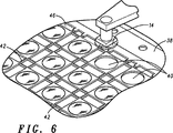
図5は、光センサ装置10を形成するために使用する第2のリードフレーム・パネル38の斜視図である。第2のリードフレーム・パネル38は、複数の第2のリードフレーム16を含む。第2のリードフレーム・パネル38および第2のリードフレーム16は、それぞれ、第1のリードフレーム・パネル22および第1のリードフレーム20とマッチするような大きさおよび形状を有する。それ故、図の実施形態の場合には、第2のリードフレーム・パネル38は、第2のリードフレーム16の3つの5×5マトリックスを含む。また、第1のリードフレーム・パネル22のように、第2のリードフレーム・パネル38は、銅のような金属であってもよく、プレス、スタンピングまたはエッチングにより形成することができる。第2の各リードフレーム16は、中央レンズ受け領域40を含む領域を有する(図6)。第2のリードフレームは、領域接続バー42を介して接続される。好適には、第2のリードフレーム・パネル38は、その周辺に沿って複数の間に間隔を有する孔部44を含むことが好ましい。図5は、その第1の側面上に置かれた第2のテープ46を含む第2のリードフレーム・パネル38を示す。図面中、第2のテープ46は、第2のリードフレーム・パネル38の下面上に位置する。
FIG. 5 is a perspective view of the second
図6は、第2のリードフレーム・パネル38の第2のリードフレーム16のレンズ受け領域40内にレンズ14を置くステップの拡大斜視図である。レンズ14は、透明プラスチックまたはガラスであってもよい。好適には、レンズ14は、反射しない光学品位のガラスであり、約15〜16ミルの厚さを有することが好ましい。レンズ14は、必要に応じて、光をフィルタリングする種々の材料でコーティングすることができる。レンズ14は、第2のテープ46の表面上の接着剤によりレンズ受け領域40内に固定される。第1のリードフレーム20のように、製造の際にリードフレームの位置の許容誤差を正確で厳密に制御することができるので、レンズ14を第2のリードフレーム16内に正確に設置することができる。
FIG. 6 is an enlarged perspective view of the step of placing the
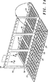
図7Aを参照すると、この図は、第1および第2のリードフレーム・パネル22および38間に、第3のリードフレーム・パネル50を置くステップを示す斜視図である。より詳細に説明すると、第3のリードフレーム・パネル50は、第1および第2のリードフレーム・パネル22および38の第2の側面間に置かれる。次に、第1および第2のリードフレーム・パネル22および38は、各IC12が接着剤の塊36により、レンズ14の対応するレンズに取り付けられるように相互に押し付けられる。さらに、押し付け動作により、IC12の表面上に接着剤の塊36が確実に均一に拡がる。第3のリードフレーム・パネル50は、IC12からレンズ14を正確に分離する働きをする。
Referring to FIG. 7A, this figure is a perspective view showing the steps of placing a third
図7Bは、第3のリードフレーム・パネル50のA−A線に沿って切断した断面図である。第3のリードフレーム・パネル50は、縁部52および中央部54を含む。中央部54は、以下に説明するように、モールド化合物を第1および第2のリードフレーム・パネル22および38の間、およびボンド・ワイヤ34の周囲に射出することができるようにする目的で、高さを低くするためにすでにエッチングされている。第3のリードフレーム・パネル50も、複数の間に間隔を有する孔部56を含む。好適には、第1、第2および第3のリードフレーム・パネル22、38および50は、すべて同じ材料からできていて、そのため同じCTE(熱膨張係数)を有することが好ましい。現在の好ましい実施形態の場合には、3つのリードフレーム・パネル22、38および50は、スタンピングしたまたはエッチングした銅からできている。
FIG. 7B is a cross-sectional view taken along the line AA of the third
図8は、リードフレーム・パネル整合ステップを示す拡大斜視図である。このステップにおいては、第1、第2および第3のリードフレーム・パネル22、38および50は、各リードフレーム・パネルの孔部24、44および56内に挿入した案内ピン58により整合している。各リードフレーム・パネルの孔部24、44および56は、各パネルの周囲の同じ位置に位置していて、パネルを正確に整合することができる。IC12およびレンズ14の両方を非常に正確に設置すると同時にパネルを正確に整合することにより、各IC12の中心とレンズ14の光軸が正確に整合するが、これは画像センサ装置を組み立てる際に非常に重要なことである。当業者であれば周知のように、レンズの光軸とセンサ画像円の中心が整合しないことが欠陥の主要な原因であり、そのため光センサの生産の際にロスが生じる。IC12およびレンズ14の両方を収容するためにリードフレームを使用しているので、本発明を使用すれば、非常に正確な設置を行うことができ、そのため整合精度が改善する。レンズ14をIC12の活性領域に接着する接着剤の塊36を硬化するために、熱硬化処理を行うことができる。
FIG. 8 is an enlarged perspective view showing a lead frame panel alignment step. In this step, the first, second and
図9は、本発明による光センサを実装するための工程の成形ステップを示す。上下の型60および62は、それぞれ第2および第1のリードフレーム・パネル38および22上に置かれる。次に、モールド化合物64が、モールド化合物64がICのボンディング・パッド66、ボンド・ワイヤ34およびリード・フィンガ18の一部をカバーするように、第1および第2のリードフレーム・パネル22および38間に射出される。すでに説明したように、第3のリードフレーム・パネル50は、第1および第2のリードフレーム・パネル22および38を分離し、IC12から所定の距離のところにレンズ14を維持する働きをする。マトリックス周囲のデバイスの場合には、この分離は第3のリードフレーム・パネル50の硬質の縁部により維持される。マトリックスの中央のユニットの場合には、射出成形工程中、射出されたモールド化合物は、中央ユニットが分離するように、第1および第2の各リードフレーム20および16を押して分離する。典型的なプラスチックIC実装工程の場合、モールド化合物射出圧力は、5トン以上で、これによりモールド化合物は確実に密にパックされる。
FIG. 9 shows the molding steps of the process for mounting the optical sensor according to the present invention. Upper and
モールド化合物64を射出し硬化した後で、第1および第2のテープ32および46が、第1および第2のリードフレーム・パネル22および38の第1の面から除去される。第1および第2のテープ32および46は、手動でまたは市販の装置で除去することができる。図10は、第1のリードフレーム・パネル22からの第1のテープ32の除去を示す。第2のテープ46も同じ方法で除去される。次に、形成されたデバイスのマトリックスが、図11の個々のデバイスを形成するためにダイシングされる。ダイシングは、当業者であれば周知のように、鋸により行うことができる。図9は、リードフレームをカットすることができる鎖線70の位置を示す。一実施形態の場合には、画像センサ装置10の全部の高さは約40ミルである。レンズ14および透明接着剤の塊36により、光はセンサIC12の活性領域を通過し、その上に入射することができる。レンズ14は第2のテープ46によりカバーされていて、レンズ上に樹脂滲みは生じない。しかし、レンズ14上に何らかの樹脂滲みが生じた場合には、そのような樹脂を除去するために後で水ジェット清掃を行うことができる。第2のテープ46も、レンズ14の潜在的な表面の掻き傷を防止する。
After injecting and curing the
図示し説明するために、本発明の好ましい実施形態について説明してきたが、この説明は全部を網羅するものでもなく、本発明を開示の形に制限するものでもない。当業者であれば、本発明の広義のコンセプトから逸脱することなしに、上記実施形態を種々に変更することができることを理解することができるだろう。それ故、本発明は、開示の特定の実施形態に限定されるものではなく、添付の特許請求の範囲に記載する本発明の精神および範囲に入る種々の修正をカバーすることを理解されたい。 For the purposes of illustration and description, the preferred embodiment of the present invention has been described above, but this description is not intended to be exhaustive or to limit the invention to the form disclosed. Those skilled in the art will appreciate that the above embodiments can be variously modified without departing from the broader concepts of the present invention. Therefore, it is to be understood that the invention is not limited to the specific embodiments disclosed, but covers various modifications that fall within the spirit and scope of the invention as set forth in the appended claims.
Claims (13)
複数の第1のリードフレームを含む第1のリードフレーム・パネルを供給するステップであって、各前記第1のリードフレームが、中央ダイ受け領域を囲んでいる複数のリード・フィンガを有するステップと、
前記第1のリードフレーム・パネルの第1の側面上に第1のテープを貼付するステップと、
複数のセンサ集積回路(IC)を供給するステップであって、各前記ICが第1の面と第2の面を有し、前記第1の面が活性領域および周辺ボンディング・パッド領域を有し、前記周辺ボンディング・パッド領域が複数のボンディング・パッドを含むステップと、
前記第1のリードフレーム・パネルの前記第1のリードフレームの各前記中央ダイ受け領域内に前記複数のICを設置するステップであって、前記ICの前記第2の面が、前記第1のテープにより前記中央ダイ受け領域内に固定されるステップと、
前記ICの各前記ボンディング・パッドおよび前記第1のリードフレームの対応するリードフレームの前記リード・フィンガを、ワイヤボンディングを介して複数のワイヤと電気的に接続し、それにより前記ICと前記第1のリードフレームを電気的に接続するステップと、
複数の第2のリードフレームを有する第2のリードフレーム・パネルを供給するステップであって、前記各第2のリードフレームが中央レンズ受け領域を有するステップと、
前記第2のリードフレーム・パネルの第1の側面上に第2のテープを貼付するステップと、
前記第2のリードフレームの各前記中央レンズ受け領域内に透明レンズを設置するステップであって、前記第2のテープにより前記透明レンズが前記中央レンズ受け領域内に固定されるステップと、
前記ICの各前記活性領域上に透明接着剤の塊を置くステップと、
第3のリードフレーム・パネルを供給するステップと、
前記第1および第2のリードフレーム・パネルの第2の側面間に前記第3のリードフレーム・パネルを設置するステップと、
前記透明接着剤の塊により各前記ICが前記透明レンズの対応する透明レンズに取り付けられるように、前記第1および第2のリードフレーム・パネルを相互の方向に押し付けるステップと、
モールド化合物が前記ボンディング・パッドおよび前記ワイヤをカバーするように、前記第1および第2のリードフレーム・パネル間に前記モールド化合物を射出するステップと、
前記第1および第2のリードフレーム・パネルの第1の側面から前記テープを除去するステップと、
前記パネルから前記リードフレームを分離し、それにより個々のデバイスを形成するステップとを含む方法。A method for mounting an optical sensor comprising:
A providing a first leadframe panel including a plurality of first lead frame, each said first lead frame, a step having a plurality of lead fingers surrounding the central die receiving area ,
Affixing a first tape on a first side of the first leadframe panel;
A providing a plurality of sensors integrated circuits (IC), each said IC having a first surface and a second surface, said first surface having an active area and a peripheral bonding pad area The peripheral bonding pad region includes a plurality of bonding pads;
A step of installing a plurality of IC to each said central die receiving area of the first lead frame of the first lead frame panel, the second surface of the IC is the first Fixed in the central die receiving area by a tape;
Said lead fingers corresponding lead frame of each of said bonding pad and the first lead frame of the IC, via wire bonding to connect a plurality of wires electrically, whereby the said IC first Electrically connecting the lead frame of
Providing a second lead frame panel having a plurality of second lead frames, each second lead frame having a central lens receiving area;
Affixing a second tape on the first side of the second leadframe panel;
Installing a transparent lens in each central lens receiving area of the second lead frame, wherein the transparent lens is fixed in the central lens receiving area by the second tape;
Placing a mass of transparent adhesive on each said active area of said IC;
Providing a third leadframe panel;
Installing the third leadframe panel between second sides of the first and second leadframe panels;
As each said IC by mass of the transparent adhesive is attached to the corresponding transparent lens of the transparent lens, comprising: pressing said first and second leadframe panels in the direction of one another,
Injecting the mold compound between the first and second leadframe panels such that a mold compound covers the bonding pad and the wire;
Removing the tape from the first side of the first and second leadframe panels;
Separating the lead frame from the panel, thereby forming individual devices.
複数のリード・フィンガにより囲まれている中央ダイ受け領域を有する第1のリードフレームと、
前記第1のリードフレームの前記中央ダイ受け領域内に配置されていて、活性領域および周辺ボンディング・パッド領域を含む第1の面を有し、前記周辺ボンディング・パッド領域が複数のボンディング・パッドを含むセンサ集積回路(IC)と、
各前記ボンディング・パッドおよび前記第1のリードフレームの対応するリードフレームのリード・フィンガにワイヤボンドされていて、それにより前記ICおよび前記第1のリードフレームを電気的に接続する複数のワイヤと、
中央レンズ受け領域を有する第2のリードフレームと、
前記第2のリードフレームの前記中央レンズ受け領域内に配置される透明レンズであって、前記第2のリードフレームが、前記透明レンズが前記ICの前記活性領域上に配置されるように、前記第1のリードフレーム上に位置している透明レンズと、
前記ICに前記透明レンズを固定する前記ICの前記活性領域上に配置される透明接着剤と、
前記第1および第2のリードフレーム間および前記ワイヤボンド上に射出されたモールド化合物とを備える画像センサ装置。An image sensor device,
A first lead frame having a central die receiving area surrounded by a plurality of lead fingers;
The first lead frame is disposed in the central die receiving region and has a first surface including an active region and a peripheral bonding pad region, and the peripheral bonding pad region includes a plurality of bonding pads. A sensor integrated circuit (IC) including:
A plurality of wires that are wire bonded to lead fingers of corresponding bonding of each said bonding pad and said first lead frame, thereby electrically connecting said IC and said first lead frame;
A second lead frame having a central lens receiving area;
A second of said central lens receiving transparent lens disposed in the region of the lead frame, so that the second lead frame, wherein the transparent lens is disposed on the active region of the IC, the A transparent lens positioned on the first lead frame;
A transparent adhesive disposed on the active region of the IC for fixing the transparent lens to the IC,
An image sensor device comprising: a molding compound injected between the first and second lead frames and on the wire bond.
Applications Claiming Priority (3)
| Application Number | Priority Date | Filing Date | Title |
|---|---|---|---|
| US10/752,159 | 2004-01-06 | ||
| US10/752,159 US6905910B1 (en) | 2004-01-06 | 2004-01-06 | Method of packaging an optical sensor |
| PCT/US2005/000057 WO2005067657A2 (en) | 2004-01-06 | 2005-01-03 | Method of packaging an optical sensor |
Publications (2)
| Publication Number | Publication Date |
|---|---|
| JP2007518275A JP2007518275A (en) | 2007-07-05 |
| JP4925832B2 true JP4925832B2 (en) | 2012-05-09 |
Family
ID=34634541
Family Applications (1)
| Application Number | Title | Priority Date | Filing Date |
|---|---|---|---|
| JP2006549338A Expired - Fee Related JP4925832B2 (en) | 2004-01-06 | 2005-01-03 | Method for mounting an optical sensor |
Country Status (6)
| Country | Link |
|---|---|
| US (2) | US6905910B1 (en) |
| JP (1) | JP4925832B2 (en) |
| KR (1) | KR101106329B1 (en) |
| CN (1) | CN100495689C (en) |
| TW (1) | TWI344218B (en) |
| WO (1) | WO2005067657A2 (en) |
Families Citing this family (14)
| Publication number | Priority date | Publication date | Assignee | Title |
|---|---|---|---|---|
| US6995462B2 (en) * | 2003-09-17 | 2006-02-07 | Micron Technology, Inc. | Image sensor packages |
| US20090026567A1 (en) * | 2004-07-28 | 2009-01-29 | Industrial Technology Research Institute | Image sensor package structure and method for fabricating the same |
| US7223626B2 (en) * | 2004-08-19 | 2007-05-29 | Micron Technology, Inc. | Spacers for packaged microelectronic imagers and methods of making and using spacers for wafer-level packaging of imagers |
| US20080283952A1 (en) * | 2005-12-24 | 2008-11-20 | Choi Hyun-Kyu | Semiconductor Package, Method of Fabricating the Same and Semiconductor Package Module For Image Sensor |
| TWI376774B (en) * | 2007-06-08 | 2012-11-11 | Cyntec Co Ltd | Three dimensional package structure |
| US7714418B2 (en) * | 2007-07-23 | 2010-05-11 | National Semiconductor Corporation | Leadframe panel |
| CN101488476B (en) * | 2009-02-25 | 2011-06-22 | 苏州晶方半导体科技股份有限公司 | Encapsulation method |
| EP2551749A1 (en) * | 2011-07-26 | 2013-01-30 | Research in Motion Corporation | Optical navigation modules for mobile communication devices |
| DE102012109156A1 (en) * | 2012-09-27 | 2014-03-27 | Osram Opto Semiconductors Gmbh | Component arrangement and method for producing electrical components |
| US20140312450A1 (en) * | 2013-04-23 | 2014-10-23 | Sensors Unlimited, Inc. | Small Size, Weight, and Packaging of Image Sensors |
| US9368423B2 (en) * | 2013-06-28 | 2016-06-14 | STATS ChipPAC Pte. Ltd. | Semiconductor device and method of using substrate with conductive posts and protective layers to form embedded sensor die package |
| US10498943B2 (en) | 2015-07-09 | 2019-12-03 | Ams Sensors Singapore Pte. Ltd. | Optoelectronic modules including overmold supporting an optical assembly |
| TWI562011B (en) * | 2016-03-09 | 2016-12-11 | Chipmos Technologies Inc | Optical fingerprint sensor package structure |
| DE102018200140A1 (en) * | 2018-01-08 | 2019-07-11 | Robert Bosch Gmbh | Environmental sensor, environmental sensor intermediate, and method of manufacturing a variety of environmental sensors |
Citations (2)
| Publication number | Priority date | Publication date | Assignee | Title |
|---|---|---|---|---|
| JPH1174555A (en) * | 1997-08-28 | 1999-03-16 | Sharp Corp | Electronic circuit element |
| US6822326B2 (en) * | 2002-09-25 | 2004-11-23 | Ziptronix | Wafer bonding hermetic encapsulation |
Family Cites Families (19)
| Publication number | Priority date | Publication date | Assignee | Title |
|---|---|---|---|---|
| US6011294A (en) | 1996-04-08 | 2000-01-04 | Eastman Kodak Company | Low cost CCD packaging |
| US6117705A (en) | 1997-04-18 | 2000-09-12 | Amkor Technology, Inc. | Method of making integrated circuit package having adhesive bead supporting planar lid above planar substrate |
| US6034429A (en) | 1997-04-18 | 2000-03-07 | Amkor Technology, Inc. | Integrated circuit package |
| US6395582B1 (en) | 1997-07-14 | 2002-05-28 | Signetics | Methods for forming ground vias in semiconductor packages |
| US5962810A (en) | 1997-09-09 | 1999-10-05 | Amkor Technology, Inc. | Integrated circuit package employing a transparent encapsulant |
| JPH1197656A (en) | 1997-09-22 | 1999-04-09 | Fuji Electric Co Ltd | Semiconductor photosensor device |
| JP2991172B2 (en) | 1997-10-24 | 1999-12-20 | 日本電気株式会社 | Semiconductor device |
| AU6000699A (en) | 1998-12-02 | 2000-06-19 | Hitachi Limited | Semiconductor device, method of manufacture thereof, and electronic device |
| US6274927B1 (en) | 1999-06-03 | 2001-08-14 | Amkor Technology, Inc. | Plastic package for an optical integrated circuit device and method of making |
| WO2001015237A1 (en) | 1999-08-20 | 2001-03-01 | Amkor Technology, Inc. | Chip-sized optical sensor package |
| US6266197B1 (en) | 1999-12-08 | 2001-07-24 | Amkor Technology, Inc. | Molded window array for image sensor packages |
| US6384472B1 (en) | 2000-03-24 | 2002-05-07 | Siliconware Precision Industries Co., Ltd | Leadless image sensor package structure and method for making the same |
| US6285064B1 (en) * | 2000-03-28 | 2001-09-04 | Omnivision Technologies, Inc. | Chip scale packaging technique for optical image sensing integrated circuits |
| US6342406B1 (en) | 2000-11-15 | 2002-01-29 | Amkor Technology, Inc. | Flip chip on glass image sensor package fabrication method |
| US6627482B2 (en) * | 2001-02-09 | 2003-09-30 | Harvatek Corporation | Mass production technique for surface mount optical device with a focusing cup |
| US6667543B1 (en) * | 2002-10-29 | 2003-12-23 | Motorola, Inc. | Optical sensor package |
| JP2004319530A (en) * | 2003-02-28 | 2004-11-11 | Sanyo Electric Co Ltd | Optical semiconductor device and its manufacturing process |
| US6995462B2 (en) * | 2003-09-17 | 2006-02-07 | Micron Technology, Inc. | Image sensor packages |
| US6856014B1 (en) * | 2003-12-29 | 2005-02-15 | Texas Instruments Incorporated | Method for fabricating a lid for a wafer level packaged optical MEMS device |
-
2004
- 2004-01-06 US US10/752,159 patent/US6905910B1/en not_active Expired - Fee Related
- 2004-12-27 TW TW093140802A patent/TWI344218B/en not_active IP Right Cessation
-
2005
- 2005-01-03 JP JP2006549338A patent/JP4925832B2/en not_active Expired - Fee Related
- 2005-01-03 KR KR1020067013500A patent/KR101106329B1/en not_active IP Right Cessation
- 2005-01-03 WO PCT/US2005/000057 patent/WO2005067657A2/en active Application Filing
- 2005-01-03 CN CNB2005800039392A patent/CN100495689C/en not_active Expired - Fee Related
- 2005-03-16 US US11/082,078 patent/US20050156301A1/en not_active Abandoned
Patent Citations (2)
| Publication number | Priority date | Publication date | Assignee | Title |
|---|---|---|---|---|
| JPH1174555A (en) * | 1997-08-28 | 1999-03-16 | Sharp Corp | Electronic circuit element |
| US6822326B2 (en) * | 2002-09-25 | 2004-11-23 | Ziptronix | Wafer bonding hermetic encapsulation |
Also Published As
| Publication number | Publication date |
|---|---|
| US20050146001A1 (en) | 2005-07-07 |
| US20050156301A1 (en) | 2005-07-21 |
| JP2007518275A (en) | 2007-07-05 |
| WO2005067657A2 (en) | 2005-07-28 |
| KR101106329B1 (en) | 2012-01-18 |
| TW200532929A (en) | 2005-10-01 |
| KR20070005933A (en) | 2007-01-10 |
| CN100495689C (en) | 2009-06-03 |
| TWI344218B (en) | 2011-06-21 |
| CN1914723A (en) | 2007-02-14 |
| US6905910B1 (en) | 2005-06-14 |
| WO2005067657A3 (en) | 2006-04-06 |
Similar Documents
| Publication | Publication Date | Title |
|---|---|---|
| US20050156301A1 (en) | Method of packaging an optical sensor | |
| KR101031394B1 (en) | Optical sensor package | |
| KR100652375B1 (en) | Image sensor module structure comprising a wire bonding package and method of manufacturing the same | |
| US5622873A (en) | Process for manufacturing a resin molded image pick-up semiconductor chip having a window | |
| US5923958A (en) | Method for semiconductor chip packaging | |
| US8058098B2 (en) | Method and apparatus for fabricating a plurality of semiconductor devices | |
| JP4452235B2 (en) | Package structure and manufacturing method thereof | |
| US7888179B2 (en) | Semiconductor device including a semiconductor chip which is mounted spaning a plurality of wiring boards and manufacturing method thereof | |
| JPH0685222A (en) | Solid-state image sensing device | |
| US20050184404A1 (en) | Photosensitive semiconductor package with support member and method for fabricating the same | |
| US20070126916A1 (en) | Image sensor chip packaging method | |
| WO1998044547A1 (en) | Method for manufacturing semiconductor device | |
| US8293572B2 (en) | Injection molding system and method of chip package | |
| US8003426B2 (en) | Method for manufacturing package structure of optical device | |
| JP2003332542A (en) | Semiconductor device and method of manufacturing the same | |
| US7781259B2 (en) | Method of manufacturing a semiconductor using a rigid substrate | |
| US20020048851A1 (en) | Process for making a semiconductor package | |
| JPH06342816A (en) | Semiconductor device, its manufacture, and lead frame used therefor | |
| KR100820913B1 (en) | Semiconductor package, method of fabricating the same and semiconductor package module for image sensor | |
| KR100456815B1 (en) | Semiconductor package and method for attaching chip | |
| KR100369394B1 (en) | substrate for semiconductor package and manufacturing method of semiconductor package using it | |
| KR100365054B1 (en) | substrate for semiconductor package and manufacturing method of semiconductor package using it | |
| KR20000008454A (en) | Pin grid array package and fabricating method of the same | |
| KR20090012445U (en) | Window clamp for Wire Bonding of Semiconductor | |
| KR20000028357A (en) | Frame for semiconductor package and method for producing semiconductor package using frame |
Legal Events
| Date | Code | Title | Description |
|---|---|---|---|
| A621 | Written request for application examination |
Free format text: JAPANESE INTERMEDIATE CODE: A621 Effective date: 20071017 |
|
| A711 | Notification of change in applicant |
Free format text: JAPANESE INTERMEDIATE CODE: A711 Effective date: 20100706 |
|
| A131 | Notification of reasons for refusal |
Free format text: JAPANESE INTERMEDIATE CODE: A131 Effective date: 20110301 |
|
| A521 | Request for written amendment filed |
Free format text: JAPANESE INTERMEDIATE CODE: A523 Effective date: 20110601 |
|
| A711 | Notification of change in applicant |
Free format text: JAPANESE INTERMEDIATE CODE: A712 Effective date: 20111014 |
|
| TRDD | Decision of grant or rejection written | ||
| A01 | Written decision to grant a patent or to grant a registration (utility model) |
Free format text: JAPANESE INTERMEDIATE CODE: A01 Effective date: 20120124 |
|
| A01 | Written decision to grant a patent or to grant a registration (utility model) |
Free format text: JAPANESE INTERMEDIATE CODE: A01 |
|
| A61 | First payment of annual fees (during grant procedure) |
Free format text: JAPANESE INTERMEDIATE CODE: A61 Effective date: 20120207 |
|
| FPAY | Renewal fee payment (event date is renewal date of database) |
Free format text: PAYMENT UNTIL: 20150217 Year of fee payment: 3 |
|
| R150 | Certificate of patent or registration of utility model |
Free format text: JAPANESE INTERMEDIATE CODE: R150 |
|
| R250 | Receipt of annual fees |
Free format text: JAPANESE INTERMEDIATE CODE: R250 |
|
| LAPS | Cancellation because of no payment of annual fees |