JP2004282019A - Lithographic marker structure, lithographic projection apparatus comprising such lithographic marker structure, and method for substrate alignment using such lithographic marker structure - Google Patents
Lithographic marker structure, lithographic projection apparatus comprising such lithographic marker structure, and method for substrate alignment using such lithographic marker structure Download PDFInfo
- Publication number
- JP2004282019A JP2004282019A JP2003366659A JP2003366659A JP2004282019A JP 2004282019 A JP2004282019 A JP 2004282019A JP 2003366659 A JP2003366659 A JP 2003366659A JP 2003366659 A JP2003366659 A JP 2003366659A JP 2004282019 A JP2004282019 A JP 2004282019A
- Authority
- JP
- Japan
- Prior art keywords
- marker structure
- marker
- substrate
- structural elements
- sensor
- Prior art date
- Legal status (The legal status is an assumption and is not a legal conclusion. Google has not performed a legal analysis and makes no representation as to the accuracy of the status listed.)
- Granted
Links
Images


Classifications
-
- G—PHYSICS
- G03—PHOTOGRAPHY; CINEMATOGRAPHY; ANALOGOUS TECHNIQUES USING WAVES OTHER THAN OPTICAL WAVES; ELECTROGRAPHY; HOLOGRAPHY
- G03F—PHOTOMECHANICAL PRODUCTION OF TEXTURED OR PATTERNED SURFACES, e.g. FOR PRINTING, FOR PROCESSING OF SEMICONDUCTOR DEVICES; MATERIALS THEREFOR; ORIGINALS THEREFOR; APPARATUS SPECIALLY ADAPTED THEREFOR
- G03F9/00—Registration or positioning of originals, masks, frames, photographic sheets or textured or patterned surfaces, e.g. automatically
- G03F9/70—Registration or positioning of originals, masks, frames, photographic sheets or textured or patterned surfaces, e.g. automatically for microlithography
- G03F9/7003—Alignment type or strategy, e.g. leveling, global alignment
- G03F9/7046—Strategy, e.g. mark, sensor or wavelength selection
-
- G—PHYSICS
- G03—PHOTOGRAPHY; CINEMATOGRAPHY; ANALOGOUS TECHNIQUES USING WAVES OTHER THAN OPTICAL WAVES; ELECTROGRAPHY; HOLOGRAPHY
- G03F—PHOTOMECHANICAL PRODUCTION OF TEXTURED OR PATTERNED SURFACES, e.g. FOR PRINTING, FOR PROCESSING OF SEMICONDUCTOR DEVICES; MATERIALS THEREFOR; ORIGINALS THEREFOR; APPARATUS SPECIALLY ADAPTED THEREFOR
- G03F9/00—Registration or positioning of originals, masks, frames, photographic sheets or textured or patterned surfaces, e.g. automatically
- G03F9/70—Registration or positioning of originals, masks, frames, photographic sheets or textured or patterned surfaces, e.g. automatically for microlithography
- G03F9/7049—Technique, e.g. interferometric
-
- G—PHYSICS
- G03—PHOTOGRAPHY; CINEMATOGRAPHY; ANALOGOUS TECHNIQUES USING WAVES OTHER THAN OPTICAL WAVES; ELECTROGRAPHY; HOLOGRAPHY
- G03F—PHOTOMECHANICAL PRODUCTION OF TEXTURED OR PATTERNED SURFACES, e.g. FOR PRINTING, FOR PROCESSING OF SEMICONDUCTOR DEVICES; MATERIALS THEREFOR; ORIGINALS THEREFOR; APPARATUS SPECIALLY ADAPTED THEREFOR
- G03F9/00—Registration or positioning of originals, masks, frames, photographic sheets or textured or patterned surfaces, e.g. automatically
- G03F9/70—Registration or positioning of originals, masks, frames, photographic sheets or textured or patterned surfaces, e.g. automatically for microlithography
- G03F9/7065—Production of alignment light, e.g. light source, control of coherence, polarization, pulse length, wavelength
-
- G—PHYSICS
- G03—PHOTOGRAPHY; CINEMATOGRAPHY; ANALOGOUS TECHNIQUES USING WAVES OTHER THAN OPTICAL WAVES; ELECTROGRAPHY; HOLOGRAPHY
- G03F—PHOTOMECHANICAL PRODUCTION OF TEXTURED OR PATTERNED SURFACES, e.g. FOR PRINTING, FOR PROCESSING OF SEMICONDUCTOR DEVICES; MATERIALS THEREFOR; ORIGINALS THEREFOR; APPARATUS SPECIALLY ADAPTED THEREFOR
- G03F9/00—Registration or positioning of originals, masks, frames, photographic sheets or textured or patterned surfaces, e.g. automatically
- G03F9/70—Registration or positioning of originals, masks, frames, photographic sheets or textured or patterned surfaces, e.g. automatically for microlithography
- G03F9/7073—Alignment marks and their environment
- G03F9/7076—Mark details, e.g. phase grating mark, temporary mark
-
- G—PHYSICS
- G03—PHOTOGRAPHY; CINEMATOGRAPHY; ANALOGOUS TECHNIQUES USING WAVES OTHER THAN OPTICAL WAVES; ELECTROGRAPHY; HOLOGRAPHY
- G03F—PHOTOMECHANICAL PRODUCTION OF TEXTURED OR PATTERNED SURFACES, e.g. FOR PRINTING, FOR PROCESSING OF SEMICONDUCTOR DEVICES; MATERIALS THEREFOR; ORIGINALS THEREFOR; APPARATUS SPECIALLY ADAPTED THEREFOR
- G03F9/00—Registration or positioning of originals, masks, frames, photographic sheets or textured or patterned surfaces, e.g. automatically
- G03F9/70—Registration or positioning of originals, masks, frames, photographic sheets or textured or patterned surfaces, e.g. automatically for microlithography
- G03F9/7073—Alignment marks and their environment
- G03F9/7084—Position of mark on substrate, i.e. position in (x, y, z) of mark, e.g. buried or resist covered mark, mark on rearside, at the substrate edge, in the circuit area, latent image mark, marks in plural levels
-
- G—PHYSICS
- G03—PHOTOGRAPHY; CINEMATOGRAPHY; ANALOGOUS TECHNIQUES USING WAVES OTHER THAN OPTICAL WAVES; ELECTROGRAPHY; HOLOGRAPHY
- G03F—PHOTOMECHANICAL PRODUCTION OF TEXTURED OR PATTERNED SURFACES, e.g. FOR PRINTING, FOR PROCESSING OF SEMICONDUCTOR DEVICES; MATERIALS THEREFOR; ORIGINALS THEREFOR; APPARATUS SPECIALLY ADAPTED THEREFOR
- G03F9/00—Registration or positioning of originals, masks, frames, photographic sheets or textured or patterned surfaces, e.g. automatically
- G03F9/70—Registration or positioning of originals, masks, frames, photographic sheets or textured or patterned surfaces, e.g. automatically for microlithography
- G03F9/7088—Alignment mark detection, e.g. TTR, TTL, off-axis detection, array detector, video detection
-
- G—PHYSICS
- G03—PHOTOGRAPHY; CINEMATOGRAPHY; ANALOGOUS TECHNIQUES USING WAVES OTHER THAN OPTICAL WAVES; ELECTROGRAPHY; HOLOGRAPHY
- G03F—PHOTOMECHANICAL PRODUCTION OF TEXTURED OR PATTERNED SURFACES, e.g. FOR PRINTING, FOR PROCESSING OF SEMICONDUCTOR DEVICES; MATERIALS THEREFOR; ORIGINALS THEREFOR; APPARATUS SPECIALLY ADAPTED THEREFOR
- G03F9/00—Registration or positioning of originals, masks, frames, photographic sheets or textured or patterned surfaces, e.g. automatically
- G03F9/70—Registration or positioning of originals, masks, frames, photographic sheets or textured or patterned surfaces, e.g. automatically for microlithography
- G03F9/7092—Signal processing
Abstract
Description
本発明は、請求項1のプリアンブルに定義するマーカ構造、前記マーカ構造を使用するウエハ位置合わせ用装置を備えるリソグラフィ投影機器および前記マーカ構造を使用してウエハを位置合わせする方法に関する。 The present invention relates to a marker structure as defined in the preamble of claim 1, a lithographic projection apparatus comprising an apparatus for aligning a wafer using said marker structure, and a method for aligning a wafer using said marker structure.
本発明は、放射投影ビームを供給する放射システムと、所望のパターンに従って投影ビームをパターン化するように働くパターン化手段を支持する支持構造と、基板を保持する基板テーブルと、基板の目標部分上にパターン化したビームを投影する投影システムとを含むリソグラフィ投影機器分野に適用される。 The present invention relates to a radiation system for providing a radiation projection beam, a support structure for supporting patterning means serving to pattern the projection beam according to a desired pattern, a substrate table for holding a substrate, and a target portion of the substrate. And a projection system for projecting a patterned beam into a lithographic projection apparatus.
ここで使用する「パターン化手段」という用語は、基板のターゲット部分に形成すべきパターンに相当するパターン化した横断面を、入射する放射ビームに付与するのに使用することができる複数の手段を指すものと広く解釈すべきである。ここでは、「光バルブ」という用語を使用することもある。一般に、前記パターンは、集積回路その他のデバイス(下記参照)など、ターゲット部分に形成されるデバイス中の特定の機能層に相当する。こうしたパターン化手段には、以下の例が含まれる。
−マスク:マスクの概念はリソグラフィにおいては周知であり、2値型、交互配置型位相シフト、ハーフトーン位相シフト、ならびに様々なハイブリッド・マスク型などのマスク・タイプの例が含まれる。こうしたマスクを放射ビーム中に配置することにより、マスク上のパターンに従って、マスク上に入射する放射を、選択的に透過(透過型マスクの場合)または反射(反射型マスクの場合)させる。マスクの場合、一般に、支持構造はマスク・テーブルであり、それによって入射する放射ビーム中で所望の位置にマスクを保持し、望まれる場合には、マスクがビームに対して相対的に移動できるようにする。
−プログラム可能なミラー・アレイ:このようなデバイスの一例は、粘弾性制御層および反射面を有するマトリックス・アドレス可能型表面である。こうした機器の基礎となる基本原理は、(たとえば)反射面のアドレスされた区域は入射光を回折光として反射し、アドレスされない区域は入射光を非回折光として反射するというものである。適当なフィルタを使用して、前記非回折光をフィルタリングして反射光から除去し、回折光のみを後に残すことができる。このようにして、マトリックス・アドレス可能型表面のアドレス・パターンに従ってビームがパターン化される。また、プログラム可能なミラー・アレイの代替実施形態では、適切な局所電界を印加し、あるいは圧電作動手段を使用することによってそれぞれ独立にある軸の周りで傾けることができる小ミラーのマトリックス構成を使用する。この場合も、ミラーはマトリックス・アドレス可能型であり、そのためアドレスされたミラーは、アドレスされないミラーとは異なる方向に、入射する放射ビームを反射する。このようにして、反射ビームは、マトリックス・アドレス可能型ミラーのアドレス・パターンに従ってパターン化される。必要とされるマトリックス・アドレス指定は、適当な電子的手段を使用して行うことができる。上記のいずれの状況でも、パターン化手段は、1つまたは複数のプログラム可能なミラー・アレイを備えることができる。ここで言及したミラー・アレイに関するより多くの情報は、たとえば、米国特許第5,296,891号および第5,523,193号、ならびにPCT特許出願WO98/38597号およびWO98/33096号から得ることができる。参照によりこれらを本明細書に合体する。プログラム可能なミラー・アレイの場合、前記支持構造は、たとえばフレームまたはテーブルとして実施することができ、必要に応じて、固定あるいは移動可能とすることができる。
−プログラム可能なLCDアレイ:このような構造の一例が、米国特許第5,229,872号に示されている。参照によりこれを本明細書に合体する。上記の場合と同様に、この場合の支持構造も、たとえばフレームまたはテーブルとして実施することができ、必要に応じて、固定あるいは移動可能とすることができる。
As used herein, the term "patterning means" refers to a plurality of means that can be used to impart an incoming radiation beam with a patterned cross-section corresponding to a pattern to be formed on a target portion of the substrate. Should be interpreted broadly as pointing. The term "light valve" is sometimes used herein. Generally, the said pattern will correspond to a particular functional layer in a device being created in the target portion, such as an integrated circuit or other device (see below). Such patterning means include the following examples.
-Mask: The concept of mask is well known in lithography and includes examples of mask types such as binary, interleaved phase shift, halftone phase shift, and various hybrid mask types. By arranging such a mask in the radiation beam, radiation incident on the mask is selectively transmitted (for a transmissive mask) or reflected (for a reflective mask) according to the pattern on the mask. In the case of a mask, generally, the support structure is a mask table, which holds the mask in a desired position in the incoming radiation beam and, if desired, allows the mask to move relative to the beam. To
A programmable mirror array: an example of such a device is a matrix-addressable surface with a viscoelastic control layer and a reflective surface. The basic principle underlying such devices is that (for example) the addressed areas of the reflective surface reflect the incident light as diffracted light, and the unaddressed areas reflect the incident light as undiffracted light. Using an appropriate filter, the undiffracted light can be filtered out of the reflected light, leaving only the diffracted light behind. In this way, the beam is patterned according to the address pattern of the matrix-addressable mold surface. Also, alternative embodiments of the programmable mirror array use a matrix configuration of small mirrors, each of which can be independently tilted about an axis by applying an appropriate local electric field or by using piezoelectric actuation means. I do. Again, the mirrors are matrix-addressable, such that addressed mirrors reflect an incoming radiation beam in a different direction than unaddressed mirrors. In this way, the reflected beam is patterned according to the address pattern of the matrix-addressable mirror. The required matrix addressing can be performed using any suitable electronic means. In any of the above situations, the patterning means may comprise one or more programmable mirror arrays. More information on the mirror arrays referred to herein can be gleaned, for example, from U.S. Pat. Can be. These are incorporated herein by reference. In the case of a programmable mirror array, the support structure may be embodied, for example, as a frame or a table and may be fixed or movable as required.
-Programmable LCD array: An example of such a structure is shown in U.S. Patent No. 5,229,872. This is incorporated herein by reference. As in the above case, the support structure in this case can also be embodied as a frame or table, for example, and can be fixed or movable as required.
簡単にするために、本明細書の残りの部分は、ある個所では、具体的にはマスクおよびマスク・テーブルを含む例を取り上げる。しかし、こうした例で論じる一般原理は、上記のパターン化手段のより広い状況の中で理解すべきである。 For simplicity, the rest of this text may, at certain locations, specifically direct itself to examples involving a mask and mask table; However, the general principles discussed in these examples should be understood in the broader context of the patterning means described above.
リソグラフィ投影機器は、たとえばIC(集積回路)の製造に使用することができる。この場合、パターン化手段は、ICの個々の層に対応する回路パターンを生成することができ、これらのパターンを、放射感受性材料(レジスト)の層を塗布した基板(シリコン・ウエハ)上の(たとえば1つまたは複数のダイを含む)ターゲット部分上に結像させることができる。一般に、1枚のウエハは、投影システムにより1度に1つずつ次々に照射される網目状に並んだ隣接するターゲット部分全体を含んでいる。マスク・テーブル上のマスクによってパターン形成を行う現在の機器では、2つの異なるタイプの機械を区別することができる。1つのタイプのリソグラフィ投影機器では、1回でマスク・パターン全体をターゲット部分上に露光することによって、各ターゲット部分を照射する。通常、このような機器をウエハ・ステッパまたはステップ・アンド・リピート機器と称する。通常ステップ・アンド・スキャン機器と称する代替機器では、投影ビーム下でマスク・パターンを所与の基準方向(「走査」方向)に順次走査することによって各ターゲット部分を照射し、基板テーブルをこの基準方向と平行または逆平行に同期走査する。一般に、投影システムは倍率M(一般に1未満)を有するので、基板テーブルを走査する速度Vは、マスク・テーブルを走査する速度のM倍となる。ここで述べたリソグラフィ装置に関するより多くの情報は、たとえば、米国特許第6,046,792号から得ることができる。参照によりこれを本明細書に合体する。 Lithographic projection equipment can be used, for example, in the manufacture of ICs (integrated circuits). In this case, the patterning means can generate circuit patterns corresponding to the individual layers of the IC, and apply these patterns on a substrate (silicon wafer) coated with a layer of radiation-sensitive material (resist). (E.g., including one or more dies). In general, a single wafer will contain a whole network of adjacent target portions that are successively irradiated via the projection system, one at a time. In current equipment for patterning with a mask on a mask table, two different types of machines can be distinguished. In one type of lithographic projection apparatus, each target portion is irradiated by exposing the entire mask pattern onto the target portion at one time. Such equipment is commonly referred to as a wafer stepper or step and repeat equipment. An alternative, commonly referred to as a step-and-scan instrument, illuminates each target portion by sequentially scanning the mask pattern under a projection beam in a given reference direction (the "scan" direction) and moves the substrate table to this reference Scan synchronously in parallel or antiparallel to the direction. In general, since the projection system has a magnification factor M (generally less than 1), the speed V of scanning the substrate table will be M times the speed of scanning the mask table. More information on the lithographic apparatus described herein can be gleaned, for example, from US Pat. No. 6,046,792. This is incorporated herein by reference.
リソグラフィ投影機器を使用する製造プロセスでは、放射感受性材料(レジスト)の層で少なくとも部分的に覆われた基板上に、(たとえばマスク内の)パターンを結像させる。この結像ステップの前に、基板に様々な処理、たとえば、プライミング、レジスト塗布、およびソフト・ベークを施すことがある。露光後、基板を、その他の処理、たとえば、PEB(露光後ベーク)、現像、ハード・ベーク、および画像形成したフィーチャーの測定/検査にかけることがある。この一連の処理をベースとして使用して、デバイスたとえばICの個々の層のパターン形成を行う。次いで、このようなパターン形成された層を、様々なプロセス、たとえば、エッチング、イオン注入(ドーピング)、メタライゼーション、酸化、化学機械研磨などにかけることができる。これらの処理はどれも、個々の層を完成させるためのものである。複数の層が必要とされる場合には、それぞれ新しい層ごとにこの処理全体またはその変形を繰り返さなければならない。最終的に、デバイス・アレイが基板(ウエハ)上に得られる。次いで、これらのデバイスを、ダイシングまたはソーイングなどの技術によって互いに分離し、その後、個々のデバイスをキャリア上に実装し、ピンに接続する、などを行うことができる。こうしたプロセスに関するさらなる情報は、たとえば、Peter van Zant著「Microchip Fabrication:A Practical Guide to Semiconductor Processing」、Third Edition、McGraw Hill Publishing Co.、ISBN 0−07−067250−4、1997年から得ることができる。参照によりこれを本明細書に合体する。 In a manufacturing process using lithographic projection equipment, a pattern (eg, in a mask) is imaged onto a substrate that is at least partially covered by a layer of radiation-sensitive material (resist). Prior to this imaging step, the substrate may be subjected to various processes, such as priming, resist coating, and soft baking. After exposure, the substrate may be subjected to other processing, for example, PEB (post exposure bake), development, hard bake, and measurement / inspection of the imaged features. This series of processes is used as a basis to pattern individual layers of a device, eg, an IC. Such a patterned layer can then be subjected to various processes, for example, etching, ion implantation (doping), metallization, oxidation, chemical mechanical polishing, and the like. All of these processes are for completing individual layers. If multiple layers are required, the entire process, or a variant thereof, must be repeated for each new layer. Eventually, a device array will be obtained on the substrate (wafer). The devices can then be separated from one another by techniques such as dicing or sawing, after which the individual devices can be mounted on a carrier, connected to pins, and so on. Further information on such processes can be found, for example, in Peter Van Zant, "Microchip Fabrication: A Practical Guide to Semiconductor Processing," Third Edition, McGraw Hill Publishing Co., Ltd. , ISBN 0-07-067250-4, 1997. This is incorporated herein by reference.
簡単にするため、以下では、投影システムを「レンズ」と称する。しかし、この用語は、たとえば、屈折光学系、反射光学系、および反射屈折型システムを含む様々なタイプの投影システムを包含すると広く解釈すべきである。また、放射システムは、これらの設計タイプのいずれかに従って動作する構成要素を含み、放射投影ビームを方向づけ、整形し、または制御することができる。下記では、このような構成要素も総称してあるいは単独で「レンズ」と称する。 For simplicity, in the following the projection system will be referred to as a "lens". However, the term should be interpreted broadly to encompass various types of projection systems, including, for example, refractive optics, catoptric optics, and catadioptric systems. The radiation system may also include components that operate according to any of these design types to direct, shape, or control the radiation projection beam. In the following, such components are also collectively or individually referred to as “lenses”.
さらに、リソグラフィ機器は、2つ以上の基板テーブル(および/または2つ以上のマスク・テーブル)を有するタイプのものとすることもできる。このような「マルチ・ステージ」型の装置では、追加のテーブルを並列で使用し、あるいは準備ステップを1つまたは複数のテーブル上で実施しながら、1つまたは複数の他のテーブルを使用して露光を行うことができる。複式ステージ・リソグラフィ機器が、たとえば、米国特許第5,969,441号および国際公開WO98/40791号に記載されている。参照によりこれらを本明細書に合体する。 Further, the lithographic apparatus may be of a type having two or more substrate tables (and / or two or more mask tables). In such a "multi-stage" type device, additional tables may be used in parallel or one or more other tables may be used while the preparation steps are performed on one or more tables. Exposure can be performed. Dual stage lithography equipment is described, for example, in U.S. Pat. No. 5,969,441 and WO 98/40791. These are incorporated herein by reference.
リソグラフィ・プロセスでは、マスク上のマスク・パターンで加工されるウエハの位置合わせは、基板上にフィーチャーを正確に画定するためにできるだけ精確に行われるべきであり、これらすべてのフィーチャーは指定の公差内のサイズを有するべきである。そのために、リソグラフィ投影機器は、所与の(指定の)公差内でマスクおよびマスク・パターンに基板を位置合わせするウエハ位置合わせモジュールを備える。一般に、ウエハ位置合わせシステムは、光学的手段に基づいてこの位置合わせを行う。ウエハあるいはウエハの一部の位置は、光源で照明される光学マーカからの光学的な応答を測定することによって求める。たとえば、レーザ・ビームでグレーティングを照明し、そのレーザ・ビームをグレーティングで回折させ、1つまたは複数の回折次数を、一般に基準面上に配置されたそれぞれのセンサで測定する。センサの出力を用いて、(基準面に対する相対的な)ウエハの位置を導き出すことができる。 In a lithographic process, the alignment of the wafer being processed by the mask pattern on the mask should be as accurate as possible to accurately define the features on the substrate, all of which are within specified tolerances. Should have a size of To that end, the lithographic projection apparatus includes a wafer alignment module that aligns the substrate with the mask and the mask pattern within given (specified) tolerances. Generally, wafer alignment systems make this alignment based on optical means. The position of the wafer or a portion of the wafer is determined by measuring the optical response from an optical marker illuminated by a light source. For example, a grating is illuminated with a laser beam, the laser beam is diffracted by the grating, and one or more diffraction orders are measured with respective sensors typically located on a reference plane. The output of the sensor can be used to derive the position of the wafer (relative to the reference plane).
従来技術では、光学マーカは、完全に可視スペクトル範囲内の波長を有する入射光を回折させるのに適した周期のグレーティングを備える。典型的な周期は16μmである。一般に、グレーティングはラインおよびトレンチで構築する。一般に、ライン幅およびトレンチ幅は、それぞれ8μmである。グレーティングから十分な回折光を得、明確な回折の極大および極小を得るために、グレーティングは最低限の数のラインおよび中間トレンチを含んでいなければならない。周期構造方向のサイズは約750μmである。 In the prior art, an optical marker comprises a grating of a period suitable for diffracting incident light having a wavelength completely within the visible spectral range. A typical period is 16 μm. Generally, gratings are constructed with lines and trenches. Generally, the line width and the trench width are each 8 μm. In order to obtain sufficient diffracted light from the grating and to obtain distinct diffraction maxima and minima, the grating must include a minimum number of lines and intermediate trenches. The size in the direction of the periodic structure is about 750 μm.
グレーティングは、グレーティングの上面で散乱する光線の位相と、グレーティングの下面で散乱する光線の位相の位相差を考慮する位相型グレーティングまたは位相マーカでよい。 The grating may be a phase grating or phase marker that takes into account the phase difference between the phase of the light scattered on the upper surface of the grating and the phase of the light scattered on the lower surface of the grating.
また、グレーティングは、グレーティングの周期構造しか考慮せず、グレーティング中の上下の高さに関係する別の位相差をもたない振幅型グレーティングでもよい。一般に、振幅型グレーティングまたは振幅マーカは、表面の高さは同様であるが、反射率がそれぞれ異なる第1および第2要素の周期構造で構築される。 Further, the grating may be an amplitude type grating that considers only the periodic structure of the grating and does not have another phase difference related to the vertical height in the grating. Generally, an amplitude type grating or an amplitude marker is constructed of a periodic structure of first and second elements having the same surface height but different reflectivities.
光学マーカは、完全な製造ラインの途中で、超小型電子デバイスの加工(またはICの加工)中に使用する。FEOL(フロント・エンド・ライン)では、トランジスタ構造の製造中の位置合わせにマーカを使用する。BEOL(バック・エンド・ライン)の後半段階では、マーカは、メタライゼーション構造、たとえば接続線およびバイアの位置合わせに必要である。いずれの場合でも、マーカの完全性が位置合わせの要求精度を満たすのに十分でなければならないことに留意されたい。 Optical markers are used during the processing of microelectronic devices (or the processing of ICs) in the middle of a complete manufacturing line. In FEOL (Front End Line), markers are used for alignment during fabrication of the transistor structure. In the second half of BEOL (Back End Line), markers are required for metallization structures, such as alignment of connection lines and vias. Note that in each case, the integrity of the marker must be sufficient to meet the required accuracy of the alignment.
半導体製造プロセス中、ウエハは、アニール、エッチング、研磨など複数の処理にかけられ、そのため、マーカの粗さ(マーカ内の陥凹領域および/またはマーカの反り)が生じることがある。このようなマーカの粗さにより、像の位置合わせ誤差が生じ、それが半導体デバイスを構築する際の重ね合わせ誤差に寄与する。また、後続の加工段階で、マーカの質が劣化する傾向があることも考えられる。 During the semiconductor manufacturing process, the wafer is subjected to multiple processes, such as annealing, etching, polishing, etc., which may result in marker roughness (recessed areas in the marker and / or warpage of the marker). Such marker roughness causes an image alignment error, which contributes to an overlay error when constructing a semiconductor device. It is also conceivable that the quality of the marker tends to deteriorate in the subsequent processing stage.
従来技術の光学マーカの欠点は、ICの加工中に、光学マーカの位相深さを制御するのが難しいことである。その結果、所与の回折角の回折光強度が弱く、ゼロに近くなることさえあり、回折ビームの正確な測定が難しく、または不可能なことさえあり得る。位相深さは、所与の回折角において、グレーティングのライン上面とトレンチ上面の間の分離した高さの差と定義することができる。(最適条件のもとで)回折強度が極大値になることが期待されるある回折角において、位相深さが照射される放射の半波長に等しい場合、回折波間の干渉の結果、低いあるいはゼロの強度が得られることになる。 A disadvantage of the prior art optical markers is that it is difficult to control the phase depth of the optical markers during IC processing. As a result, the intensity of the diffracted light at a given diffraction angle may be weak, even close to zero, and accurate measurement of the diffracted beam may be difficult or even impossible. The phase depth can be defined as the differential height difference between the top of the line of the grating and the top of the trench at a given diffraction angle. At certain diffraction angles where the diffraction intensity is expected to be at a maximum (under optimal conditions), if the phase depth is equal to half the wavelength of the illuminated radiation, the result of interference between the diffracted waves is low or zero. Will be obtained.
IC加工中の位相深さの制御は、ウエハ間のプロセス変動のため難しく、また単一ウエハ全体でも難しいことがある。 Controlling the phase depth during IC processing is difficult due to process variations between wafers, and can be difficult even across a single wafer.
従来技術のマーカの別の欠点は、マーカ下の1つ(または複数)の層の作用としてマーカ特性が依存することから生じる。半導体デバイスに見られる様々な層の様々な光学的挙動のためにマーカのコントラストが変化することがあり、その結果、下の層の作用として回折強度の変化が生じることが知られている。 Another disadvantage of prior art markers arises from the dependence of the marker properties as a function of the layer (s) under the marker. It is known that the contrast of a marker can change due to the different optical behavior of the different layers found in semiconductor devices, resulting in a change in the diffraction intensity as a function of the underlying layer.
さらに、様々な加工ステップが、位置合わせマーカの形状に悪影響を及ぼすことがあることも知られている。形状へのこうした影響のために、このような改変されたマーカによる位置合わせでは、改変されたマーカ形状が、生成される回折ビーム(パターン)を変化させることから生じ得る誤差が含まれることがある。 It is further known that various processing steps can adversely affect the shape of the alignment marker. Because of such effects on shape, alignment with such modified markers may include errors that can result from the altered marker shape changing the generated diffraction beam (pattern). .
さらに、従来技術では、BEOLプロセス中に、表面に見えていた残余の構造により、キャップ層下で光学マーカを検出することができるはずである。しかし、CMP(化学機械研磨)などの平坦化プロセスを適用するため、多くの場合、位置合わせに残余のマーカ構造を使用するという任意選択は不可能になった。 Furthermore, in the prior art, during the BEOL process, the residual structure that was visible on the surface should be able to detect the optical marker under the cap layer. However, the application of a planarization process such as CMP (chemical mechanical polishing) has often made the option of using the remaining marker structure for alignment impossible.
従来技術では、タングステンで充填したトレンチを備える半導体基板上のマーカは、CMPプロセスにかけられて表面からタングステンが除去され、表面が平坦化される。CMPプロセスのため、タングステン構造は、充填状態あるいは不完全充填状態になる。充填の程度は、マーカによって生成される光学信号の位相深さに関係する。すなわち、2つの離散位相深さレベルが存在する。一方のレベルは、浅く小さな位相深さを有する充填タングステン構造に関係するものであり、他方のレベルは、比較的深く大きな位相深さを有する不完全充填タングステン構造に関係するものである。小さな位相深さによって生じる位置合わせ誤差は比較的大きいので、充填マーカの小さな位相深さは望ましくない。また、大きな位相深さにより、位置合わせ誤差が小さくなることも保証されない。すなわち、位相深さにより、光学信号の消失が生じることがある。さらに、位相深さの制御を実現することはできない。 In the prior art, a marker on a semiconductor substrate having a trench filled with tungsten is subjected to a CMP process to remove tungsten from the surface and planarize the surface. Due to the CMP process, the tungsten structure is in a filled or incompletely filled state. The degree of filling is related to the phase depth of the optical signal generated by the marker. That is, there are two discrete phase depth levels. One level relates to a filled tungsten structure having a shallow and small phase depth, and the other level relates to an incompletely filled tungsten structure having a relatively deep and large phase depth. Since the registration error caused by a small phase depth is relatively large, a small phase depth of the fill marker is undesirable. Also, a large phase depth does not guarantee that alignment errors will be small. That is, the optical signal may be lost depending on the phase depth. Further, control of the phase depth cannot be realized.
本来、光学マーカは集積回路のフィーチャー・サイズよりも大きいので、光学マーカがIC加工に及ぼす影響により、望ましくない副作用が生じることがある。従来技術では、マーカの最小フィーチャー・サイズは1μm程度である。現在の超小型電子デバイスでは、典型的な最小フィーチャー・サイズは、(デバイスの世代によって決まり)約100nmである。一般に、マーカはデバイス(の一部)と同じ材料からなるので、デバイスの近傍に大きなサイズの追加のマーカ領域が存在すると、所与の加工ステップにおいて、そのデバイスの局所的な加工速度に影響を及ぼすことがある。たとえば、反応性イオン・エッチング加工または化学的成長プロセスにおける化学反応は、ある種の動力学的な制約あるいはウエハ温度の局所的な偏差などのために、大きなマーカ領域の存在の影響を受けることがある。すなわち、マーカとデバイス・フィーチャーのサイズの差により、たとえば、マーカ近くに位置するデバイスの加工ステップの改変が生じることがある。加工の改変のため、ダイおよび/またはウエハ全体にわたってデバイス特性のばらつきが生じることがある。 Since optical markers are inherently larger than the feature size of the integrated circuit, the effects of the optical markers on IC processing can have undesirable side effects. In the prior art, the minimum feature size of the marker is on the order of 1 μm. For current microelectronic devices, a typical minimum feature size is about 100 nm (depending on device generation). In general, the markers are made of the same material as (part of) the device, so the presence of a large size additional marker area near the device will affect the local processing speed of that device in a given processing step. May have an effect. For example, chemical reactions in reactive ion etching or chemical growth processes can be affected by the presence of large marker areas due to certain kinetic constraints or local variations in wafer temperature. is there. That is, a difference in size between the marker and the device feature may cause, for example, modification of the processing steps of a device located near the marker. Due to processing modifications, device characteristics may vary across the die and / or wafer.
本明細書では、本発明による機器をICの製造で使用することを特に参照しているが、こうした機器を他の可能な応用例に適用できることをはっきりと理解されたい。たとえば、集積光学系、磁気ドメイン・メモリ、液晶ディスプレイ・パネル、薄膜磁気ヘッド用の誘導/検出パターンなどの製造で使用することができる。こうした代替応用例の状況では、本明細書において使用する「レチクル」、「ウエハ」あるいは「ダイ」という用語を、それぞれ「マスク」、「基板」および「目標部分」というより一般的な用語で置き換えて考えるべきであることが当業者には理解されよう。 Although particular reference is made herein to the use of devices according to the invention in the manufacture of ICs, it should be clearly understood that such devices can be applied to other possible applications. For example, it can be used in the manufacture of integrated optics, magnetic domain memories, liquid crystal display panels, guidance / detection patterns for thin film magnetic heads, and the like. In the context of such alternative applications, the terms "reticle", "wafer" or "die" as used herein are replaced by the more general terms "mask", "substrate" and "target portion", respectively. It will be appreciated by those skilled in the art that this should be considered.
この文章では、「放射」および「投影ビーム」という用語は、(たとえば、365、248、193、157または126nmの波長を有する)UV(紫外)放射、および(たとえば、5〜20nmの範囲の波長を有する)EUV(極紫外)放射を含むあらゆるタイプの電磁放射を包含するものとして使用する。 In this text, the terms “radiation” and “projection beam” refer to UV (ultraviolet) radiation (eg, having a wavelength of 365, 248, 193, 157, or 126 nm), and wavelengths (eg, in the range of 5-20 nm). Used to include all types of electromagnetic radiation, including EUV (extreme ultraviolet) radiation.
本発明の目的は、回折パターン内の弱め合う干渉を防止するように位相深さを補正することができるマーカ構造を提供することである。 An object of the present invention is to provide a marker structure that can correct the phase depth so as to prevent destructive interference in the diffraction pattern.
本発明の第1態様では、この目的は、第1構造要素が第1レベル上に第1反射面を有し、第2構造要素がほぼ非反射性であり、
第2反射面がより下方の第2レベル上に位置し、
前記第1および第2反射面の間隔が検出光の位相深さ条件を決め、
陥凹部(R1;R2;R3)が前記第2反射面内に存在し、それによって前記位相条件が改変されることを特徴とする、請求項1のプリアンブルに定義する基板の光学的位置合わせ用の基板上マーカ構造において達成される。
In a first aspect of the invention, the object is that the first structural element has a first reflective surface on a first level, the second structural element is substantially non-reflective,
A second reflective surface located on a lower second level;
An interval between the first and second reflection surfaces determines a phase depth condition of the detection light;
2. The optical alignment of a substrate as defined in the preamble of claim 1, wherein a recess (R1; R2; R3) is present in the second reflecting surface, whereby the phase condition is modified. In the on-substrate marker structure.
この陥凹領域は、十分な強度の強め合う干渉がセンサで観測されるようになる量だけ位相深さを変更する。 The recessed region changes the phase depth by an amount such that constructive interference of sufficient intensity is observed at the sensor.
本発明の第2態様では、この目的は、第1構造要素が第1レベル上に第1反射面を有し、第2構造要素がほぼ非反射性であり、
第2反射面がより下方の第2レベル上に位置し、
前記第1および第2反射面の間隔が検出光の位相深さ条件を決め、
前記第2反射面が、不透明な層の上に位置する複数の追加の構造要素を備えることを特徴とする、請求項9のプリアンブルに定義する基板の光学的位置合わせ用の基板上マーカ構造において達成される。
In a second aspect of the invention, the object is that the first structural element has a first reflective surface on the first level, the second structural element is substantially non-reflective,
A second reflective surface located on a lower second level;
An interval between the first and second reflection surfaces determines a phase depth condition of the detection light;
10. The on-substrate marker structure for optical alignment of a substrate as defined in the preamble of claim 9, wherein said second reflective surface comprises a plurality of additional structural elements located on an opaque layer. Achieved.
マーカ構造を互いに上に積み重ねることによって、下にある層の作用として検出された強度の変動が減少すると有利である。強め合う干渉を伴う最適位相深さを有するように、中間誘電層を調整することができる。 Advantageously, stacking the marker structures on top of each other reduces variations in intensity detected as a function of the underlying layer. The intermediate dielectric layer can be tuned to have an optimal phase depth with constructive interference.
本発明の別の目的は、プロセスにより生じる損傷を監視することができるマーカ構造を提供することである。 It is another object of the present invention to provide a marker structure that can monitor damage caused by the process.
この目的は、マーカ構造が第1周期構造および第2周期構造を備え、
第2周期構造が第1周期構造に隣接しかつ平行であり、
第1周期構造が、複数の第1材料の第1構造要素および複数の第2材料の第2構造要素を備え、第1および第2構造要素が繰返し順序で配置され、第1の幅が第2の幅よりも大きく、
第2周期構造が、第3の幅を有する複数の第2材料の第1構造要素および第4の幅を有する複数の第1材料の第2構造要素を備え、第1および第2構造要素が繰返し順序で配置され、第3の幅が第1の幅に等しく、第4の幅が第2の幅に等しく、
第2周期構造中の第1構造要素が、第2周期構造が第1周期構造と相補的になるように、第1周期構造中の第1構造要素に隣接して位置することを特徴とする、請求項10のプリアンブルに定義する基板の光学的位置合わせ用の基板上マーカ構造において達成される。
For this purpose, the marker structure comprises a first periodic structure and a second periodic structure,
A second periodic structure is adjacent and parallel to the first periodic structure;
The first periodic structure includes a plurality of first structural elements of a first material and a plurality of second structural elements of a second material, wherein the first and second structural elements are arranged in a repeating order and have a first width equal to a first width. Larger than the width of 2,
The second periodic structure comprises a plurality of first structural elements of a second material having a third width and a plurality of second structural elements of a first material having a fourth width, wherein the first and second structural elements are Arranged in a repeating order, wherein the third width is equal to the first width, the fourth width is equal to the second width,
The first structural element in the second periodic structure is located adjacent to the first structural element in the first periodic structure such that the second periodic structure is complementary to the first periodic structure. This is achieved in an on-substrate marker structure for optical alignment of the substrate as defined in the preamble of
第1周期構造と、それと相補的な第2周期構造とを備える相補的な構造により、第1および第2周期構造中の第1または第2構造要素のいずれかに損傷が生じると、第1周期構造と第2周期構造とでは回折パターンが異なって変化することになるので、この位置合わせシステムを使用することにより、IC加工シーケンスによって周期構造中の構造要素の1つが損傷を受けたかどうかを監視することが可能になる。 When a damage occurs to any of the first or second structural elements in the first and second periodic structures due to a complementary structure including the first periodic structure and a second periodic structure complementary to the first periodic structure, the first periodic structure is provided. Since the diffraction pattern changes differently between the periodic structure and the second periodic structure, the use of this alignment system determines whether one of the structural elements in the periodic structure has been damaged by the IC processing sequence. It becomes possible to monitor.
本発明の別の目的は、マーカ構造を含む下にある層をCMPプロセスにかけるためにメタライゼーション層から残余のマーカ構造が除去されることを克服するマーカ構造を提供することである。この目的は、前記マーカ構造がメタライゼーション層中に存在し、
前記第1構造要素が第1表面状態を有する第1表面領域部分からなり、
前記第2構造要素が第2表面状態を有する第2表面領域部分からなり、
前記第1表面領域部分が第1埋込みマーカ要素に関係し、
前記第2表面領域部分が第2埋込みマーカ要素に関係し、
前記第1および第2表面状態が、それぞれ前記第1埋込みマーカ要素および前記第2埋込みマーカ要素によって生じる前記メタライゼーション層の形態の変化に関係することを特徴とする、請求項14のプリアンブルに定義するマーカ構造において達成される。
It is another object of the present invention to provide a marker structure that overcomes the removal of residual marker structures from a metallization layer for subjecting an underlying layer containing the marker structures to a CMP process. For this purpose, the marker structure is present in the metallization layer,
The first structural element comprises a first surface region portion having a first surface state;
The second structural element comprises a second surface region portion having a second surface state;
The first surface area portion is associated with a first embedded marker element;
The second surface area portion is associated with a second embedded marker element;
15. The preamble of claim 14, wherein the first and second surface states relate to a change in morphology of the metallization layer caused by the first embedded marker element and the second embedded marker element, respectively. Is achieved in the marker structure.
下にある材料の作用としての表面状態/形態の差異がメタライゼーション層中に作り出されるように、メタライゼーション層を被着させると有利である。この表面の表面状態/形態の周期変化は、位置合わせシステムおよび/または重ね合わせシステムにより検出可能である。 It is advantageous to apply the metallization layer such that differences in surface state / morphology as a function of the underlying material are created in the metallization layer. This periodic change in the surface state / morphology of the surface can be detected by the registration system and / or the overlay system.
本発明の目的は、比較的大きなマーカ領域の近傍に位置するデバイス・フィーチャーへのこのような大きなマーカ領域によって生じる影響に打ち勝つマーカ構造を提供することである。 It is an object of the present invention to provide a marker structure that overcomes the effects caused by such large marker areas on device features located near the relatively large marker areas.
この目的は、前記第1構造要素が複数の1次ラインおよび複数の第1挿入ラインを備えることを特徴とする、請求項19のプリアンブルに定義するマーカ構造において達成される。 This object is achieved in a marker structure as defined in the preamble of claim 19, characterized in that said first structuring element comprises a plurality of primary lines and a plurality of first insertion lines.
マーカ構造を構築する構造要素がそれぞれ、製品のフィーチャー・サイズに匹敵する固有のサイズを有する副要素にさらに分割されると有利である。製品のフィーチャー・サイズを模倣しそれにより近づけることによって、サイズにより生じる加工の影響が最小限に抑えられる。 Advantageously, the structural elements that make up the marker structure are each further divided into sub-elements having a unique size comparable to the feature size of the product. By mimicking and approximating the feature size of the product, the processing effects caused by the size are minimized.
さらに、本発明の目的は、上記で述べたマーカ構造を適用することができるリソグラフィ投影機器を提供することである。 It is a further object of the present invention to provide a lithographic projection apparatus to which the above-described marker structure can be applied.
さらに、本発明の目的は、上記で述べたマーカ構造を使用するリソグラフィ投影機器において、基板を位置合わせする方法を提供することである。 It is a further object of the present invention to provide a method for aligning a substrate in a lithographic projection apparatus that uses the marker structure described above.
以下に、複数の図面を参照して本発明を説明するが、これらの図面は単なる例であり、添付の特許請求の範囲に定義する保護の範囲を限定するものではない。 In the following, the invention will be described with reference to several drawings, which are by way of example only and do not limit the scope of protection defined in the appended claims.
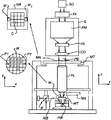
図1に、本発明の特定の実施例による少なくとも1つのマーカ構造を備えるリソグラフィ投影機器1を概略的に示す。この機器は、
放射投影ビームPB(たとえばUV放射)を供給する放射システムEx、ILを備える。この特定の例では、放射システムは放射源SOも備える。
マスクMA(たとえばレチクル)を保持するマスク・ホルダを備え、第1位置決め手段(図示せず)に連結されて要素PLに対してマスクを正確に位置決めする第1対象物テーブル(マスク・テーブル)MTと、
基板W(たとえばレジストを塗布したシリコン・ウエハ)を保持する基板ホルダを備え、第2位置決め手段PWに連結されて要素PLに対して基板を正確に位置決めする第2対象物テーブル(基板テーブル)WTと、
基板Wの(たとえば1つまたは複数のダイを含む)ターゲット部分C上に、マスクMAの照射された部分を結像する投影システム(「レンズ」)PLとを備える。
FIG. 1 schematically shows a lithographic projection apparatus 1 comprising at least one marker structure according to a particular embodiment of the invention. This equipment is
It comprises a radiation system Ex, IL which supplies a radiation projection beam PB (eg UV radiation). In this particular example, the radiation system also comprises a radiation source SO.
A first object table (mask table) MT provided with a mask holder for holding a mask MA (for example, a reticle) and coupled to first positioning means (not shown) for accurately positioning the mask with respect to the element PL; When,
A second object table (substrate table) WT which includes a substrate holder for holding a substrate W (for example, a silicon wafer coated with a resist) and is connected to the second positioning means PW to accurately position the substrate with respect to the element PL; When,
A projection system ("lens") PL for imaging an illuminated portion of a mask MA on a target portion C (eg, including one or more dies) of a substrate W.
ここで示すように、この機器は、透過タイプの(すなわち、透過型マスクを有する)ものである。しかし、一般に、たとえば(反射型マスクを備える)反射タイプのものとすることもできる。あるいは、この機器では、別の種類のパターン化手段、たとえば上記で言及したタイプのプログラム可能なミラー・アレイを使用することもできる。 As here shown, the device is of a transmissive type (ie has a transmissive mask). However, in general, it can also be of a reflective type, for example (with a reflective mask). Alternatively, the instrument may use another kind of patterning means, for example a programmable mirror array of the type mentioned above.
放射源SO(たとえば、水銀ランプまたはエキシマ・レーザ)は、放射ビームを生成する。このビームを、直接、あるいはビーム・エキスパンダExなどの調節手段を通った後に、照明システム(照明器)IL内に供給する。照明器ILは、ビームの強度分布の外側および/または内側半径方向範囲(通常、それぞれ外側σおよび内側σと称する)を設定する調節手段AMを備えることができる。さらに、一般に、照明器ILは、様々な他の構成要素、たとえば統合器INおよびコンデンサCOも備えている。このようにして、マスクMA上に入射するビームPBは、所望の均一性および強度分布をその横断面に有する。 A source SO (eg, a mercury lamp or excimer laser) produces a beam of radiation. This beam is fed into the illumination system (illuminator) IL, either directly or after having passed through conditioning means such as a beam expander Ex. The illuminator IL may comprise adjusting means AM for setting the outer and / or inner radial extent (commonly referred to as outer σ and inner σ, respectively) of the intensity distribution of the beam. Further, in general, the illuminator IL also includes various other components, such as an integrator IN and a capacitor CO. In this way, the beam PB incident on the mask MA has the desired uniformity and intensity distribution in its cross section.
図1を参照すると、(放射源SOが、たとえば水銀ランプであるときはしばしばそうであるが)、放射源SOを、このリソグラフィ投影機器のハウジング内に置くことができるが、リソグラフィ投影機器から離し、放射源LAが生成する放射ビームを(たとえば適当な方向づけミラーによって)機器内に導入することもできることに留意されたい。後者の状況が生じるのは、しばしば放射源SOがエキシマ・レーザのときである。本発明および特許請求の範囲は、どちらの状況も包含するものとする。 Referring to FIG. 1, the source SO can be placed within the housing of the lithographic projection apparatus, but often apart from the lithographic projection apparatus (as is often the case when the source SO is, for example, a mercury lamp). Note that the radiation beam produced by the radiation source LA can also be introduced into the instrument (for example by means of a suitable directing mirror). The latter situation often occurs when the source SO is an excimer laser. The invention and claims are intended to cover both situations.
その後、ビームPBは、マスク・テーブルMT上に保持されるマスクMAに当たる。マスクMAを横切ったビームPBは、レンズPLを通過し、基板Wのターゲット部分C上に結像する。第2位置決め手段PWおよび干渉計測手段により、基板テーブルWTは正確に動き、たとえば異なるターゲット部分CをビームPBの経路内に位置決めすることができる。同様に、(マスク・テーブルMTで作用する)第1位置決め手段を使用して、たとえば、マスク・ライブラリからマスクMAを機械的に取り出した後、あるいは走査中に、ビームPBの経路に対してマスクMAを正確に位置決めすることができる。一般に、対象物テーブルMT、WTの移動は、長ストローク・モジュール(粗い位置決め用)および短ストローク・モジュール(精密位置決め用)によって行われる。これらのモジュールは、図1に明示的に示していない。ただし、ウエハ・ステッパの場合には(ステップ・アンド・スキャン機器と異なり)、マスク・テーブルMTを、短ストローク・アクチュエータだけに連結するか、あるいは固定とすることもできる。マスクMAおよび基板Wは、マスク位置合わせマークM1、M2および基板位置合わせマークP1、P2を使用して位置合わせすることができる。 Thereafter, the beam PB strikes the mask MA, which is held on the mask table MT. The beam PB traversing the mask MA passes through the lens PL and forms an image on the target portion C of the substrate W. By means of the second positioning means PW and the interference measuring means, the substrate table WT can move accurately, for example, to position different target portions C in the path of the beam PB. Similarly, using the first positioning means (acting on the mask table MT), for example, after mechanical removal of the mask MA from the mask library or during scanning, the mask may be moved relative to the path of the beam PB. The MA can be accurately positioned. In general, movement of the object tables MT, WT is performed by a long-stroke module (for coarse positioning) and a short-stroke module (for fine positioning). These modules are not explicitly shown in FIG. However, in the case of a wafer stepper (as opposed to a step-and-scan device) the mask table MT may be connected to a short-stroke actuator only, or may be fixed. The mask MA and the substrate W can be aligned using the mask alignment marks M1, M2 and the substrate alignment marks P1, P2.
図の機器は、下記の2つの異なるモードで使用することができる。
1.ステップ・モードでは、マスク・テーブルMTはほぼ固定したまま、ターゲット部分C上にマスク像全体を1回で(すなわち1回の「フラッシュ」で)投影する。次いで、基板テーブルWTを、X方向および/またはY方向に移動し、それによってビームPBで異なるターゲット部分Cを照射することができる。
2.スキャン・モードでは、所与のターゲット部分Cが1回の「フラッシュ」で露光されない点を除き、ほぼ同じ状況が当てはまる。その代わりに、マスク・テーブルMTが、所与の方向(いわゆる「走査方向」、たとえばY方向)に速度vで移動可能であり、それによって、投影ビームPBがマスク像の上を走査する。それに並行して、基板テーブルWTが同時に同方向または反対方向に速度V=Mvで移動する。ただし、MはレンズPLの倍率(通常、M=1/4または1/5)である。このようにして、比較的大きなターゲット部分Cを、解像力を損なわずに露光することができる。
The illustrated device can be used in two different modes:
1. In the step mode, the entire mask image is projected on the target portion C at one time (that is, with one "flash") while the mask table MT is kept almost fixed. The substrate table WT can then be moved in the X and / or Y directions, so that different target portions C can be irradiated with the beam PB.
2. In scan mode, almost the same situation applies, except that a given target portion C is not exposed in a single "flash". Instead, the mask table MT is movable at a speed v in a given direction (the so-called "scan direction", e.g. the Y direction), whereby the projection beam PB scans over the mask image. In parallel, the substrate table WT moves simultaneously in the same or opposite direction at a speed V = Mv. Here, M is the magnification of the lens PL (usually, M = 1/4 or 1/5). In this manner, a relatively large target portion C can be exposed without impairing the resolution.
一般に、干渉計測手段は、(図示しない)レーザなどの光源および1つまたは複数の干渉計を備え、それによって、測定すべき物体、たとえば基板またはステージに関するなんらかの情報(たとえば、位置、位置合わせなど)を求めることができる。図1に、たとえば1つの干渉計IFを概略的に示す。光源(レーザ)は、1つまたは複数のビーム・マニピュレータによって干渉計IFに送られる計測ビームMBを生成する。2つ以上の干渉計が存在する場合は、各干渉計ごとに様々な別々のビームに計測ビームを分ける光学系を使用して、これらの干渉計間でこの計測ビームを共有する。 Generally, the interferometric means comprises a light source such as a laser (not shown) and one or more interferometers, whereby some information about the object to be measured, for example a substrate or a stage (eg, position, alignment, etc.) Can be requested. FIG. 1 schematically shows, for example, one interferometer IF. The light source (laser) generates a measurement beam MB that is sent to the interferometer IF by one or more beam manipulators. If more than one interferometer is present, the measurement beam is shared between the interferometers using optics that split the measurement beam into various separate beams for each interferometer.
テーブルWT上の基板をマスク・テーブルMT上のマスクMAに位置合わせする基板位置合わせシステムMSを、例えば基板テーブルWT近傍の位置で概略的に示す。基板位置合わせシステムMSは、基板上のマーカ構造に照準を合わせる光ビームを生成する少なくとも1つの光源およびこのマーカ構造からの光信号を検出する少なくとも1つのセンサ装置を備える。基板位置合わせシステムMSの位置は、リソグラフィ投影機器の実際のタイプに応じて変化し得る設計条件によって決まることに留意されたい。このマーカ構造は、たとえば、基板位置合わせマークP1、P2であり得る。 A substrate alignment system MS for aligning a substrate on a table WT with a mask MA on a mask table MT is schematically illustrated, for example, at a position near the substrate table WT. The substrate alignment system MS comprises at least one light source for generating a light beam aimed at a marker structure on the substrate and at least one sensor device for detecting a light signal from the marker structure. It should be noted that the position of the substrate alignment system MS depends on design conditions which can vary depending on the actual type of lithographic projection apparatus. This marker structure can be, for example, the substrate alignment marks P1, P2.
図2に、位相深さの概念を示す従来技術のマーカ構造の断面を概略的に示す。 FIG. 2 schematically shows a cross section of a prior art marker structure illustrating the concept of phase depth.
一般に、光学マーカ構造は、波長λの入射光を回折させるのに適した周期Pのグレーティング50を備える。この文章で「光」という用語を用いる場合、可視スペクトル内の波長に限定されず、可視波長よりも長い波長または短い波長の光も包含する。周期Pが可視スペクトル内の光の回折に適したものであることは必須でなく、本発明は、それよりも短い波長または長い波長に適した周期Pでも実施できることを理解されたい。 Generally, the optical marker structure comprises a grating 50 with a period P suitable for diffracting incident light of wavelength λ. The use of the term "light" in this text is not limited to wavelengths in the visible spectrum, but also includes light at wavelengths longer or shorter than the visible wavelength. It is to be understood that the period P need not be suitable for diffraction of light in the visible spectrum, and that the invention can be practiced with a period P suitable for shorter or longer wavelengths.
このグレーティングは、挿入トレンチ102を伴う一連のライン100からなる。トレンチ102は、ライン100の上面に対して深さdtを有する。グレーティングの周期Pは、ライン幅PIおよびトレンチ幅PIIから構成される。
This grating consists of a series of
図2では、入射光ビームλは、基板表面にほぼ直交する方向に向けられる。あるいは、直交せず傾いた入射ビームを使用してもよい。 In FIG. 2, the incident light beam λ is directed in a direction substantially orthogonal to the substrate surface. Alternatively, an incident beam that is not orthogonal and tilted may be used.
従来技術のマーカ・グレーティングは、いわゆる位相型グレーティングである。それぞれ表面に対して回折角θを有する2本の回折ビームで回折パターンを概略的に示す。 Prior art marker gratings are so-called phase gratings. The diffraction pattern is schematically illustrated by two diffraction beams, each having a diffraction angle θ with respect to the surface.
回折パターンでは、強度の極大および極小の位置は、グレーティングの周期によって決まる。入射光の波長λが可視光の範囲内にあるとき、一般に、周期Pは16μmであり、それによって位置合わせの目的に適した回折パターンが得られる。一般に、ライン幅PIおよびトレンチ幅PIIはそれぞれ8μmである。 In the diffraction pattern, the positions of the maximum and minimum intensities are determined by the grating period. When the wavelength λ of the incident light is in the range of visible light, the period P is generally 16 μm, thereby obtaining a diffraction pattern suitable for alignment purposes. Generally, the line width P I and the trench width P II are each 8 μm.
グレーティング50から十分な回折光を得、明確な回折の極大および極小の角度分布(回折パターン)を得るために、グレーティング50は、入射光ビームで照明される最低限の数のライン100および中間トレンチ102を含まなければならない。従来技術では、マーカは、照野内に少なくとも10個のトレンチを備える。
In order to obtain sufficient diffracted light from the grating 50 and to obtain a well-defined diffraction maximum and minimum angular distribution (diffraction pattern), the grating 50 comprises a minimum number of
さらに、回折ビームの強度は、ライン100の上面に対する相対的なトレンチ102の深さdtによっても決まる。ライン100の上面で散乱した光線およびトレンチ102の底面で散乱した光線は、回折光のある方向において、この方向のこれらの光線間で強め合う干渉を得るために、周期Pに無関係にある位相関係をもたなければならない。ライン100の表面に対する相対的なトレンチ102の深さdtは、強め合う干渉が生じることになるものでなければならない。干渉が弱め合う場合には、信号の消失が生じることになる。このことは、位相深さ条件として周知のものである。
Further, the intensity of the diffracted beam is also determined by the depth dt of the trench 102 relative to the top surface of the
位相型グレーティング50では、回折パターンにおける干渉は、概略的に以下のように演繹することができる。すなわち、角度θのもとで、第1の組の光子はライン100の上面で反射し、第2の組の光子はトレンチ102の床面で反射する。回折角θで示す所与の方向で強度の極大または極小が生じることになるかどうかを決定づけるには、ラインの上面から発する光子とトレンチの床面から発する光子の伝播波面PFにおける位相差がそれぞれ、ほぼゼロまたは半波長でなければならない。
In the phase grating 50, interference in the diffraction pattern can be roughly deduced as follows. That is, under the angle θ, a first set of photons reflects off the top surface of the
半導体ウエハ上の光学マーカ構造の場合、この構造は、集積回路を形成するための半導体ウエハの加工ステップ中に様々な変形を受けることがある。これらの変形のため、位相深さdtは製造中に変化することがある。 In the case of an optical marker structure on a semiconductor wafer, the structure may undergo various deformations during the processing steps of the semiconductor wafer to form an integrated circuit. Due to these deformations, the phase depth dt may change during manufacture.
図3aに、従来技術のマーカ構造の断面を概略的に示す。図3aでは、銅ベースの超小型電子デバイス用のIC加工のBEOL(バック・エンド・ライン)で利用することができる基板層SL上の光学マーカ構造OMを示す。一般に、こうしたデバイスは、(光学的に透明な)誘電体材料中に銅構造を埋め込み、それが「フローティング・マーカ」のように見える、いわゆる銅ダマシン加工技術によって製造される。光学マーカ50は、誘電体材料中に埋め込まれた複数の銅のライン要素104からなり、この誘電体材料は複数のライン要素106に整形される。一般に、当業者には周知なように、この誘電体材料は、様々な別々の誘電体層のスタックからなり得る。誘電体スタック中で様々な別々の誘電体層の厚さが変動するため、成り行きで、マーカ50の位相深さdtが明確に画定されないことがある。さらに、ダイまたはウエハ全体にわたって変動が存在することもある。したがって、最悪の場合、回折パターン中に含まれるマーカ信号の強度が弱すぎて、位置合わせツールによる検出ができないことがある。このため、IC加工中に、マーカの不合格あるいはウエハの不合格さえ生じることがある。
FIG. 3a schematically shows a cross section of a prior art marker structure. FIG. 3a shows an optical marker structure OM on a substrate layer SL that can be used in BEOL (Back End Line) for IC processing for copper based microelectronic devices. Generally, such devices are manufactured by so-called copper damascene technology, in which a copper structure is embedded in a (optically transparent) dielectric material, which looks like a "floating marker".
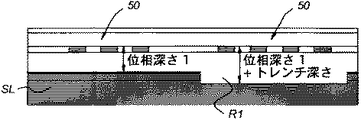
図3bに、本発明によるマーカ構造の第1実施例の断面を示す。 FIG. 3b shows a cross section of a first embodiment of the marker structure according to the invention.
図3bには、不適合な位相深さによる消失を回避する方法を示す。図3bで、同じ参照番号の要素は、図3aに示す同じ要素を指す。FEOL(フロント・エンド・ライン)プロセス中に、フローティング・マーカ50の下の半導体基板(または一般に不透明な層)SLの領域に、陥凹部R1を生成する。この陥凹部により位相深さが増し、したがって、表面レベルと基板または不透明層のレベルからの散乱光の間で弱め合う干渉が生じる可能性が減少する。
FIG. 3b shows a method for avoiding loss due to mismatched phase depth. In FIG. 3b, elements with the same reference numbers refer to the same elements shown in FIG. 3a. During the FEOL (Front End Line) process, a recess R1 is created in the region of the semiconductor substrate (or generally opaque layer) SL below the floating
図3bに示すように、この陥凹部は、フローティング・マーカ50で覆われる領域の一部の下にのみ形成することができる。この場合、2つの異なる位相深さが存在し、その一方から十分な強度をもつより良好で使用可能な回折信号を得ることができる。
As shown in FIG. 3 b, this recess can be formed only under a part of the area covered by the floating
図3cに、本発明によるマーカ構造の第2実施例の断面を示す。 FIG. 3c shows a cross section of a second embodiment of the marker structure according to the invention.
第2実施例では、この陥凹領域は、FEOLプロセス中に、マーカ50の一部の下にのみ画定される。図3cの右側に示すように、陥凹部R2は、マーカ50の透明部分の下にしか形成されない。図3cの左側では、陥凹部R3は、マーカ50の不透明部分の下にしか形成されない。この場合も、2つの異なる位相深さが存在し、それぞれから十分な強度をもつ使用可能な回折信号が得られる。
In a second embodiment, this recessed area is defined only under a portion of the
このような陥凹領域R2、R3は、マーカ用のマスクと適当なリソグラフィ・プロセスを用いて、ポジ露光またはネガ露光でそれぞれ形成することができることに留意されたい。 It should be noted that such recessed regions R2, R3 can be formed by positive exposure or negative exposure, respectively, using a marker mask and a suitable lithography process.
図3bまたは3cに示す陥凹領域により、約200〜300nmが位相深さに追加されるのが好ましい。 Preferably, approximately 200-300 nm is added to the phase depth by the recessed region shown in FIG. 3b or 3c.
図4に、本発明によるマーカ構造の第3実施例の断面を概略的に示す。 FIG. 4 schematically shows a cross section of a third embodiment of the marker structure according to the present invention.
従来技術のマーカの別の欠点は、マーカ下の1つ(または複数)の層の作用としてマーカ特性が依存することによるものである。半導体デバイスに見られる様々な層の様々な光学的挙動のためにマーカのコントラストが変化することがあり、その結果、下の層の作用として回折強度の変化が生じる、すなわち、位相深さが下にある層の作用として大きく変化することが知られている。 Another disadvantage of the prior art markers is due to the dependence of the marker properties as a function of the layer (s) below the marker. The contrast of the marker may change due to the different optical behavior of the different layers found in the semiconductor device, resulting in a change in the diffraction intensity as a function of the underlying layer, i.e., the phase depth is reduced. It is known that the effect of the layer in the above-mentioned layer greatly changes.
本発明による第3実施例では、(露光および加工による)第1金属層中の第1光学マーカOM1を第1配列トーン、すなわち、第1構造要素および第2構造要素の所与の周期的繰返しで画定することによって、位相深さがより良好に制御される。次いで、少なくとも1つの中間誘電体層IDLとともに第1金属層上に積み重ねた第2金属層中に、第1配列トーンと同じだが第1マーカに対して逆のトーンで第2光学マーカOM2を画定(露光および加工)する。この逆のトーンは、第2マーカOM2が第1光学マーカOM1と同じ周期的繰返しを備えるが、第1構造要素および第2構造要素の位置が第1マーカOM1に対して相対的に入れ替わっていることを示す。 In a third embodiment according to the invention, the first optical marker OM1 in the first metal layer (by exposure and processing) is given a first arrangement tone, ie a given periodic repetition of the first and second structuring elements. , The phase depth is better controlled. Then, a second optical marker OM2 is defined in the second metal layer stacked on the first metal layer with at least one intermediate dielectric layer IDL with the same tone as the first array tone but opposite to the first marker. (Exposure and processing). This opposite tone is such that the second marker OM2 comprises the same periodic repetition as the first optical marker OM1, but the positions of the first and second structural elements are switched relative to the first marker OM1. It indicates that.
中間誘電体層IDLを制御することによって、位相深さを制御する、すなわち、十分な強度の回折信号が得られる位相深さの値を選択することができる。さらに、ウエハのスクライブレーン内でマーカが占めるスペースは、光学マーカを積み重ねることによって大きく減少する。 By controlling the intermediate dielectric layer IDL, the phase depth can be controlled, that is, the value of the phase depth at which a diffraction signal of sufficient intensity can be obtained can be selected. Further, the space occupied by the markers in the scribe lane of the wafer is greatly reduced by stacking the optical markers.
通常、IDLの厚さはIC加工パラメータによって決まることに留意されたい。偶然に、積み重ねたマーカ間のIDLの厚さが、基板位置合わせシステムが使用する波長で弱め合う干渉が生じる位相深さに相当する場合、第2波長を使用してよい。 Note that typically the thickness of the IDL depends on the IC processing parameters. By chance, if the thickness of the IDL between the stacked markers corresponds to the phase depth at which destructive interference occurs at the wavelength used by the substrate alignment system, the second wavelength may be used.
図5に、本発明によるマーカ構造の第4実施例のマーカ構造を斜視図で概略的に示す。 FIG. 5 schematically shows a marker structure of a fourth embodiment of the marker structure according to the present invention in a perspective view.
IC製作中の様々な加工ステップは、位置合わせマーカの形状に悪影響を及ぼすことがある。たとえば、光学マーカ構造中のラインのブロック形状は、CMPステップのために変化することがある。CMPプロセスのため、ラインの断面は非対称になる。すなわち、本質的に(局所的な)研磨方向のため、研磨により上縁部の一方しか丸くならない。 Various processing steps during IC fabrication can adversely affect the shape of the alignment marker. For example, the block shape of a line in the optical marker structure may change due to the CMP step. Due to the CMP process, the cross section of the line becomes asymmetric. That is, polishing only rounds one of the upper edges due to the essentially (local) polishing direction.
形状へのこうした影響のために、このような改変された(一方の縁部が丸められた)マーカによる位置合わせでは、改変されたマーカ形状が、生成される回折パターンを変化させることから生じる誤差が含まれることがある。一般に、マーカ形状の改変により、光学マーカ構造によって生成される回折ピークの位置が、元のマーカ形状のピーク位置に対して相対的にシフトする。従来技術では、いずれの状況でも回折パターンおよび/またはパターン中のピーク位置の変化が生じるので、純粋なマーカ位置合わせ不良とマーカ形状の改変とを区別することは不可能であった。 Because of these effects on the shape, registration with such a modified (one edge rounded) marker will result in errors that result from the modified marker shape changing the diffraction pattern generated. May be included. Generally, the modification of the marker shape shifts the position of the diffraction peak generated by the optical marker structure relative to the peak position of the original marker shape. In the prior art, it was not possible to distinguish between a pure marker misalignment and a modified marker shape, since the diffraction pattern and / or the peak position in the pattern would change in any situation.
第4実施例による光学マーカ構造により、パターンのシフトが、マーカの位置合わせ不良のためなのか、あるいはIC加工により生じたマーカの変形のためなのかを調べることが可能になり得る。 With the optical marker structure according to the fourth embodiment, it may be possible to check whether the shift of the pattern is due to the misalignment of the marker or the deformation of the marker caused by the IC processing.
この光学マーカは、第1部分に第1周期構造PS1を備え、第2部分に第2周期構造PS2を備える。第1および第2周期構造PS1およびPS2は、1方向に平行に進むそれぞれの周期で互いに隣接して配置される。 This optical marker includes a first periodic structure PS1 in a first portion and a second periodic structure PS2 in a second portion. The first and second periodic structures PS1 and PS2 are arranged adjacent to each other at respective periods proceeding in parallel in one direction.
第1周期構造PS1は、PS2と同じ周期を有するが、その構造要素の配列順序は、第2周期構造PS2と相補的である。第1周期構造PS1は、第1の幅w1を有する複数の第1材料の第1構造要素SE1および第2の幅w2を有する複数の第2材料の第2構造要素SE2からなり、それらはそれぞれ周期的に配置される。 The first periodic structure PS1 has the same period as PS2, but the arrangement order of the structural elements is complementary to the second periodic structure PS2. The first periodic structure PS1 comprises a plurality of first structural elements SE1 of a first material having a first width w1 and a plurality of second structural elements SE2 of a second material having a second width w2, each of which is They are arranged periodically.
第2周期構造PS2は、第3の幅w3を有する複数の第2材料の第3構造要素SE3および第4の幅w4を有する複数の第1材料の第4構造要素SE4からなり、それらはそれぞれ周期的に配置される。PS1はPS2と相補的なので、第1構造要素SE1は、第3の幅w3に等しい第1の幅w1で第3構造要素SE3に隣接し、第2構造要素SE2は、第4の幅w4に等しい第2の幅w2で第4構造要素SE4に隣接する。さらに、周期構造PS1およびPS2はそれぞれ非対称である。すなわち、第1および第2の幅は互いに異なる。 The second periodic structure PS2 is composed of a plurality of third structural elements SE3 of a second material having a third width w3 and a plurality of fourth structural elements SE4 of a first material having a fourth width w4, respectively. They are arranged periodically. Since PS1 is complementary to PS2, the first structural element SE1 is adjacent to the third structural element SE3 with a first width w1 equal to the third width w3, and the second structural element SE2 has a fourth width w4. Adjacent to the fourth structural element SE4 with an equal second width w2. Further, the periodic structures PS1 and PS2 are each asymmetric. That is, the first and second widths are different from each other.
例として、この光学マーカ構造は、銅を第1材料とし絶縁体を第2材料として、銅ダマシン構造として配置することができる。すなわち、銅および絶縁体の周期変化により、マーカ構造が回折格子として働く。したがって、たとえば、SE1およびSE4が銅を含み、SE2およびSE3が絶縁体を含む。SE1の幅w1はSE3の幅w3に等しく、SE2の幅w2はSE4の幅w4に等しい。 By way of example, the optical marker structure can be arranged as a copper damascene structure with copper as the first material and insulator as the second material. That is, the marker structure functions as a diffraction grating due to the periodic change of copper and the insulator. Thus, for example, SE1 and SE4 include copper, and SE2 and SE3 include insulators. The width w1 of SE1 is equal to the width w3 of SE3, and the width w2 of SE2 is equal to the width w4 of SE4.
ただし、こうしたマーカは、金属/半導体構造または金属/絶縁体構造に埋め込むこともできることに留意されたい。また、こうした相補型光学マーカ構造は、半導体基板中にエッチングし互いに隣接して配置した2つの相補的な幾何形状のグレーティング(すなわち、ラインおよびトレンチ)によって形成することもできる。 Note, however, that such markers can also be embedded in a metal / semiconductor or metal / insulator structure. Such complementary optical marker structures can also be formed by two complementary geometric gratings (ie, lines and trenches) etched into a semiconductor substrate and placed adjacent to each other.
当業者には周知のように、マーカ構造中で相補的なフィーチャーを使用すると、測定中に(ゼロ・レベルの)固定信号が得られる。周期構造PS1およびPS2がほぼ相補的である場合、第1周期構造PS1からの第1信号は、第2周期構造PS2からの第2信号に相補的なものになる。第1および第2信号は互いに弱め合い、センサで測定される第1および第2信号の合成信号は、ほぼゼロ・レベルを有することになる。 As is well known to those skilled in the art, the use of complementary features in the marker structure results in a fixed signal (zero level) during the measurement. If the periodic structures PS1 and PS2 are substantially complementary, the first signal from the first periodic structure PS1 will be complementary to the second signal from the second periodic structure PS2. The first and second signals deplete each other, and the combined signal of the first and second signals measured by the sensor will have a substantially zero level.
上記で述べた構造への加工の影響のために、第1周期構造PS1は、第2周期構造PS2と異なるしかたで変形する。というのは、両方の構造がそれぞれ異なる非対称性を有するからである。第1周期構造PS1では、金属ラインSE1は、第2周期構造PS2中の金属ラインSE4の幅w4と異なる幅w1を有し得る。それぞれの構造PS1およびPS2中の金属ラインおよび絶縁体ラインの幅の差異のため、それぞれのラインの形状の変化は異なったものになる。 Due to the influence of the processing on the structure described above, the first periodic structure PS1 is deformed differently from the second periodic structure PS2. This is because both structures have different asymmetries. In the first periodic structure PS1, the metal line SE1 may have a width w1 different from the width w4 of the metal line SE4 in the second periodic structure PS2. Due to the difference in the width of the metal lines and insulator lines in each of the structures PS1 and PS2, the shape of each line changes differently.
2つの構造がこのように異なって改変されるため、PS1からの第1信号は、もはやPS2からの第2信号と相補的ではなくなる。その結果、測定時に、相補的なグレーティングはもはやゼロ・レベルの信号を示さないことになる。その代わり、ゼロではない信号が測定されることになる。 Because the two structures are modified differently in this way, the first signal from PS1 is no longer complementary to the second signal from PS2. As a result, at the time of measurement, the complementary grating will no longer show a zero level signal. Instead, a non-zero signal will be measured.
相補的な光学マーカ構造からこのような信号が生じることにより、マーカがプロセスに関係した影響を受けたことが示される。したがって、類似の周期性を有する他のマーカへのプロセスにより生じる影響の存在およびこうした影響のドリフトを、この相補的な光学マーカ構造で監視することができると有利である。 The occurrence of such a signal from the complementary optical marker structure indicates that the marker has undergone a process related effect. It would therefore be advantageous if the presence of effects caused by the process on other markers with similar periodicity and the drift of such effects could be monitored with this complementary optical marker structure.
図6に、本発明の第5実施例によるマーカ構造の平面を示す。 FIG. 6 shows a plan view of a marker structure according to a fifth embodiment of the present invention.
ある種のICメタライゼーション・プロセスでは、表面における残余のトポグラフィのため、メタライゼーション層下の埋込みマーカ(すなわち、メタライゼーション層下の光学マーカ構造)が依然として検出可能である。この場合、マーカ構造の幾何形状、すなわち、ラインおよびトレンチはそれぞれ、メタライゼーション層表面内で、高い領域および下にある領域として依然として目視可能である。 In some IC metallization processes, embedded markers beneath the metallization layer (ie, optical marker structures under the metallization layer) are still detectable due to residual topography at the surface. In this case, the geometry of the marker structure, ie, the lines and trenches, respectively, are still visible as high and underlying regions within the metallization layer surface.
しかし、ICの加工では、タングステン・コンタクトおよびバイアの平坦化技術としてCMP(化学機械研磨)を適用する。CMPにより上面が平坦化され、残余のトポグラフィは失われる。このような場合には、残余のマーカ構造を使用して位置合わせすることは不可能である。 However, in the processing of an IC, CMP (chemical mechanical polishing) is applied as a planarization technique of a tungsten contact and a via. The top is flattened by CMP and the residual topography is lost. In such a case, it is impossible to perform registration using the remaining marker structure.
本発明の第5実施例では、振幅型マーカ構造として働くアルミニウムのメタライゼーション層中にマーカ構造を形成する。図6に、BEOLプロセス中に形成される層のスタックを示す。すなわち、トレンチ中にタングステン・コンタクトを形成する。CMPによって、タングステン・コンタクトおよび酸化物絶縁体の表面を平坦化する。平坦化した表面上にチタン接合層を被着させる。次いで、高温金属被着プロセスによってアルミニウムを被着させる。最後に、Ti/TiNのキャップ層を被着させる。図6に、それぞれの層の厚さの値のいくつかの例を示す。 In a fifth embodiment of the present invention, a marker structure is formed in an aluminum metallization layer that serves as an amplitude marker structure. FIG. 6 shows a stack of layers formed during the BEOL process. That is, a tungsten contact is formed in the trench. CMP planarizes the surfaces of the tungsten contacts and oxide insulator. A titanium bonding layer is deposited on the planarized surface. The aluminum is then deposited by a high temperature metal deposition process. Finally, a cap layer of Ti / TiN is deposited. FIG. 6 shows some examples of the thickness values of the respective layers.
メタライゼーション層は、(一般に、約350℃、UHV条件下で物理気相成長法で被着させる)高温金属プロセスを含む。タングステンを覆うチタン接合層上のアルミニウムと二酸化シリコンを覆うチタン接合層上のアルミニウムでは結晶粒成長がそれぞれ異なるため、下にある材料に応じて、アルミニウム層中に異なる表面状態が作り出される。タングステン・コンタクトすなわちプラグの上で、この表面は第1表面状態ST2を有し、酸化物の上では、この表面は第2表面状態ST1を有する。 The metallization layer comprises a high temperature metal process (generally deposited by physical vapor deposition under UHV conditions at about 350 ° C.). Since the grain growth is different for aluminum on the titanium bonding layer over tungsten and aluminum on the titanium bonding layer over silicon dioxide, different surface states are created in the aluminum layer depending on the underlying material. On a tungsten contact or plug, this surface has a first surface state ST2, and on oxide, this surface has a second surface state ST1.
おそらく、チタン層は、下にある材料に応じて異なるテクスチャを有する。このテクスチャは、高温金属被着プロセス中に被着させるアルミニウムの核形成および結晶粒成長に、タングステンを覆う領域と二酸化シリコンを覆う領域では異なる影響を及ぼすことがある。表面状態の差異は、形態上の差異、すなわち、下にある材料に応じたメタライゼーション層のテクスチャおよび/または結晶粒のサイズに関係する。あるいは、チタン層が比較的薄いので、タングステン上のアルミニウムまたは二酸化シリコン上のアルミニウムの異なる核形成および結晶粒成長も、下にある材料の熱物理特性の差異によって生じることがある。 Possibly, the titanium layer has a different texture depending on the underlying material. This texture can affect the nucleation and grain growth of aluminum deposited during the high temperature metallization process differently in the area over tungsten and the area over silicon dioxide. The differences in surface state are related to morphological differences, i.e., the texture and / or grain size of the metallization layer depending on the underlying material. Alternatively, because the titanium layer is relatively thin, different nucleation and grain growth of aluminum on tungsten or aluminum on silicon dioxide may also result from differences in the thermophysical properties of the underlying materials.
いずれの場合でも、物理化学的な原因がなんであっても、表面状態の局所的な差異は、位置合わせセンサ・システムおよび/または重ね合わせセンサ・システムによってマーカ構造として検出可能である。 In any case, whatever the physicochemical cause, local differences in surface conditions can be detected as marker structures by the alignment sensor system and / or the overlay sensor system.
こうした形態的なマーカ構造は、図6で説明した特定の構造に限定されないことに留意されたい。メタライゼーション層は、周期構造を形成する(CMP処理した)ある種の他の下にある材料によっても表面状態の周期的変化を示すことがある。 Note that these morphological marker structures are not limited to the specific structure described in FIG. The metallization layer may also exhibit periodic changes in surface state due to certain other underlying materials that form the periodic structure (CMP treated).
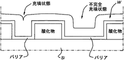
従来技術では、タングステンで充填したトレンチを備える半導体基板上のマーカは、CMPプロセスにかけられてタングステンが除去され、基板表面が平坦化される。タングステンCVDとCMPを組み合わせるため、タングステン構造は充填状態あるいは不完全充填状態になる。充填の程度は、マーカによって生成される光学信号の位相深さに関係する。すなわち、2つの離散位相深さレベルが存在する。 In the prior art, a marker on a semiconductor substrate having a trench filled with tungsten is subjected to a CMP process to remove the tungsten and planarize the substrate surface. Since tungsten CVD and CMP are combined, the tungsten structure is in a filled state or an incompletely filled state. The degree of filling is related to the phase depth of the optical signal generated by the marker. That is, there are two discrete phase depth levels.
一方のレベルは、構造の上面までほぼ完全に充填するため、浅く小さな位相深さを有する充填タングステン構造に関係するものである。 One level relates to a filled tungsten structure having a shallow, small phase depth to fill almost completely to the top surface of the structure.
他方のレベルは、比較的深く大きな位相深さを有する不完全充填タングステン構造に関係するものである。 The other level relates to an incompletely filled tungsten structure having a relatively deep and large phase depth.
小さな位相深さによって生じる位置合わせ誤差は比較的大きいので、充填マーカの小さな位相深さは望ましくない。また、大きな位相深さにより、位置合わせ誤差が小さくなることも保証されない。すなわち、位相深さにより、光学信号の消失が生じることがある。 Since the registration error caused by a small phase depth is relatively large, a small phase depth of the fill marker is undesirable. Also, a large phase depth does not guarantee that alignment errors will be small. That is, the optical signal may be lost depending on the phase depth.
図7aに、タングステンCMP前の、従来技術の充填されたタングステン・マーカおよび完全に充填されていないタングステン・マーカの断面を示す。 FIG. 7a shows a cross section of a prior art filled and completely unfilled tungsten marker prior to tungsten CMP.
二酸化シリコン層中にエッチングしたトレンチ中に、ブランケット・モードのCVDプロセスによってタングステンを被着させる。図7aに、トレンチの幅により、共形に成長させたタングステン層がトレンチを「充填」モードあるいは「不完全充填」モードで充填するのが決まる様子を示す。 Tungsten is deposited by a blanket mode CVD process into trenches etched into the silicon dioxide layer. FIG. 7a shows how the width of the trench determines whether the conformally grown tungsten layer fills the trench in a "fill" mode or an "incomplete fill" mode.
共形成長特性を有するタングステンCVD時に、狭いトレンチが「充填」トレンチになり、広いトレンチが「不完全充填」トレンチになる。 During tungsten CVD with co-formed length characteristics, narrow trenches become "filled" trenches and wide trenches become "incompletely filled" trenches.
トレンチの底面はバリア層で覆われることがある。 The bottom of the trench may be covered with a barrier layer.
次いで、CMPプロセスを行って構造を平坦化する。このようにして、二酸化シリコン表面とほぼ同じレベルの表面を有する金属(タングステン)構造を形成する。その結果、「充填」構造の位相深さはほぼゼロになる。「不完全充填」金属構造は、二酸化シリコン表面とほぼ同じレベルである部分(すなわち側壁)と、表面が二酸化シリコン表面のレベルよりもかなり下である中央部分とを備える。CMP後、中央のタングステン部分は、二酸化シリコン表面のレベルに対して相対的な所与の位相深さを有する。 Next, a CMP process is performed to planarize the structure. In this way, a metal (tungsten) structure having a surface almost at the same level as the silicon dioxide surface is formed. As a result, the phase depth of the “filled” structure is almost zero. An "incompletely filled" metal structure comprises a portion that is about the same level as the silicon dioxide surface (i.e., a sidewall) and a central portion where the surface is well below the level of the silicon dioxide surface. After CMP, the central tungsten portion has a given phase depth relative to the level of the silicon dioxide surface.
当業者には周知のように、所与のトレンチ深さおよび所与の加工パラメータを有する(すなわち、所与の厚さを有する共形タングステン層を形成する)タングステン被着プロセスでは、トレンチ幅により、タングステン・ラインが充填されるかあるいは完全には充填されないかが決まる。したがって、位相深さは、トレンチ幅の作用として、2つの離散レベルを含むことになる。さらに、タングステンおよび二酸化シリコンのCMPに対する抵抗が異なるので、CMPプロセスを極めて正確に制御することはできない。 As is well known to those skilled in the art, a tungsten deposition process having a given trench depth and given processing parameters (i.e., forming a conformal tungsten layer with a given thickness) requires a , The tungsten line is filled or not completely filled. Thus, the phase depth will include two discrete levels as a function of the trench width. In addition, due to the different resistance of tungsten and silicon dioxide to CMP, the CMP process cannot be controlled very accurately.
上記で述べたように、不完全充填金属マーカ・ラインを備えるマーカ構造では、金属ラインの中央部分の深さは、位相深さがほぼゼロになることがある。すなわち、位相深さの制御を実現することはできない。 As noted above, in a marker structure with an incompletely filled metal marker line, the depth of the central portion of the metal line may be near zero in phase depth. That is, control of the phase depth cannot be realized.
図7bに、本発明の第6実施例による二酸化シリコン中のタングステン・マーカ構造の平面図(TOP)および断面図(SIDE)を示す。 FIG. 7b shows a plan view (TOP) and a cross-sectional view (SIDE) of a tungsten marker structure in silicon dioxide according to a sixth embodiment of the present invention.
本発明の第6実施例では、光学マーカ構造は、二酸化シリコンのライン中にタングステンの副セグメントを備える。 In a sixth embodiment of the invention, the optical marker structure comprises a tungsten sub-segment in a line of silicon dioxide.
副セグメントとして、二酸化シリコンのライン中に、副トレンチの長さ方向がマーカ構造の周期Pに平行な方向に延びる複数の副トレンチを形成する。複数の副トレンチは、位置合わせ手順中にいわゆる非走査方向になる方向に周期的に配置されているので、このPsub方向の副トレンチの周期的配置による光学的な影響は、基板位置合わせシステムによって検出されない。副トレンチ(の周期性)によって生成される発生し得る回折信号は、実際のマーカ構造(すなわち、タングステン・トレンチおよび二酸化シリコン・ラインの繰返し)の回折信号の方向に直交する方向に向けられるので、この発生し得る信号は、基板位置合わせシステムによって検出されない。 As sub-segments, a plurality of sub-trenches are formed in the silicon dioxide line, the length of the sub-trench extending in a direction parallel to the period P of the marker structure. Since the plurality of sub-trenches are periodically arranged in a direction that becomes a so-called non-scanning direction during the alignment procedure, the optical effect of the periodic arrangement of the sub-trench in the Psub direction is affected by the substrate alignment system. Not detected. The possible diffraction signal generated by the sub-trench (periodicity) is directed in a direction orthogonal to the direction of the diffraction signal of the actual marker structure (ie, the repetition of the tungsten trench and silicon dioxide line), This possible signal is not detected by the substrate alignment system.
この第6実施例では、やはり、タングステンCVDプロセスによって、トレンチおよび副トレンチをタングステンで充填する。次いで、CMPプロセスを行って構造を平坦化する。副トレンチ中にタングステンが存在するため、CMPプロセスは、より良好に制御される。副トレンチを用いることによって、CMPに対して特定の抵抗を有する充填タングステン構造を備えるマーカ構造の面積は、比較的大きくなる(タングステンは酸化物よりもCMPに対してより大きな抵抗を有する)。これにより、より高い精度で所与の高さに充填トレンチを研磨することができる。不完全充填構造のより低い部分のレベルに対して相対的に充填トレンチの研磨高さをより良好に制御することによって、位相深さを制御することができる。不完全充填領域中のタングステンのより低いレベルに対する相対的な充填タングステン構造の上面レベルの高さを、所望の位相深さが得られるように適合させることができる。充填タングステン構造の相対面積を変更するために二酸化シリコンのライン中の副トレンチ間の間隔(およびその数)を変更することによって位相深さを適合させることができる。 In the sixth embodiment, the trench and the sub-trench are also filled with tungsten by the tungsten CVD process. Next, a CMP process is performed to planarize the structure. Due to the presence of tungsten in the sub-trench, the CMP process is better controlled. By using sub-trenches, the area of the marker structure with a filled tungsten structure having a particular resistance to CMP is relatively large (tungsten has a greater resistance to CMP than oxide). This allows the filling trench to be polished to a given height with higher accuracy. By better controlling the polishing height of the filled trench relative to the level of the lower part of the incompletely filled structure, the phase depth can be controlled. The height of the top level of the filled tungsten structure relative to the lower level of tungsten in the incompletely filled region can be adapted to obtain a desired phase depth. The phase depth can be tailored by changing the spacing (and number) between sub-trenches in the silicon dioxide line to change the relative area of the filled tungsten structure.
副トレンチの幅は、共形タングステン層の厚さの倍である(したがって、その結果、ゼロ位相深さを有する完全に充填された副トレンチが生じる)。 The width of the sub-trench is twice the thickness of the conformal tungsten layer (thus resulting in a completely filled sub-trench with zero phase depth).
本来、光学マーカは集積回路のフィーチャー・サイズよりも大きいので、光学マーカがIC加工に及ぼす影響により、望ましくない副作用が生じることがある。従来技術では、マーカの最小フィーチャー・サイズは1μm程度である。現在の超小型電子デバイスでは、典型的な最小フィーチャー・サイズは、(デバイスの世代によって決まり)約100nmである。一般に、マーカはデバイス(の一部)と同じ材料からなるので、デバイスの近傍に大きなサイズの追加のマーカ領域が存在すると、所与の加工ステップにおいてそのデバイスの局所的な加工速度に影響を及ぼすことがある。たとえば、反応性イオン・エッチング加工または化学的成長プロセスにおける化学反応は、ある種の動力学的な制約あるいはウエハ温度の局所的な偏差などのために、大きなマーカ領域の存在の影響を受けることがある。化学機械研磨プロセスは、マーカ領域により生じるある種の機械的な制約(すなわち、CMPに対するより大きな抵抗あるいはより小さい抵抗)のために、大きなマーカ領域の存在の影響を受けることがある。 Since optical markers are inherently larger than the feature size of the integrated circuit, the effects of the optical markers on IC processing can have undesirable side effects. In the prior art, the minimum feature size of the marker is on the order of 1 μm. For current microelectronic devices, a typical minimum feature size is about 100 nm (depending on device generation). In general, the marker is made of the same material as (part of) the device, so the presence of a large size additional marker area near the device will affect the local processing speed of that device at a given processing step Sometimes. For example, chemical reactions in reactive ion etching or chemical growth processes can be affected by the presence of large marker areas due to certain kinetic constraints or local variations in wafer temperature. is there. Chemical-mechanical polishing processes can be affected by the presence of large marker areas due to certain mechanical constraints imposed by the marker areas (ie, greater or lesser resistance to CMP).
すなわち、マーカとデバイス・フィーチャーのサイズの差により、マーカ近くに位置するデバイスの加工ステップの改変が生じることがある。加工の改変のため、ダイおよび/またはウエハ全体にわたってデバイス特性のばらつきが生じることがある。 That is, the difference in size between the marker and the device feature may alter the processing steps of the device located near the marker. Due to processing modifications, device characteristics may vary across the die and / or wafer.
IC加工の観点からみて、デバイス中の最小フィーチャー・サイズにより近く対応するようにマーカ構造要素の寸法を変更することにより、IC加工のサイズ依存性の問題を克服することができる。ただし、「ライン」および「トレンチ」の幅を変更すると、マーカの周期も変更することがある。これにより、逆に、位置合わせセンサ・システムおよび重ね合わせセンサ・システムを再設計して新しいマーカの周期に適合させるための大きな労力が必要になるはずである。 By changing the dimensions of the marker structuring element to more closely correspond to the smallest feature size in the device from an IC processing perspective, the size dependence of IC processing can be overcome. However, when the width of the “line” and “trench” is changed, the period of the marker may also be changed. This, in turn, would require a great deal of effort to redesign the alignment and overlay sensor systems to accommodate the new marker period.
さらに、位置合わせシステムは直線偏光レーザ光を用いるので、こうした位置合わせシステムでは、このような改変されたマーカ構造との相互作用から生じる偏光の影響により、逆に信号強度が大きく減少することがある。 Furthermore, since the alignment system uses linearly polarized laser light, the effect of polarization resulting from interaction with such a modified marker structure can significantly reduce signal strength in such alignment systems. .
本発明者たちは、IC加工のこのサイズ依存性を克服するために、従来技術の光学マーカ構造では、改変されたマーカ構造により生成される回折パターンが従来技術の改変されていないマーカのものとほぼ同じままでありながら、最小デバイス・フィーチャーをより良好に模倣できるようにセグメント化する必要があることを認識している。また、位置合わせシステムは、偏光の効果により、測定された信号から使用可能な信号強度が得られるように配置する。 To overcome this size dependence of IC processing, the present inventors have proposed that in prior art optical marker structures, the diffraction pattern produced by the modified marker structure be different from that of the prior art unmodified marker. It recognizes that it needs to be segmented to better mimic the smallest device features while remaining approximately the same. Also, the alignment system is arranged such that the effect of polarization results in usable signal strength from the measured signal.
図8に、本発明の第7実施例によるマーカ構造の平面を示す。 FIG. 8 shows a plan view of a marker structure according to a seventh embodiment of the present invention.
本発明の第7実施例では、第1構造要素を、1次ラインのそれぞれがデバイスの最小フィーチャー・サイズに匹敵する幅を有し、第1方向D1に延びる複数の1次ラインL1に副セグメント化する。1次ライン間には異なる材料の挿入ラインがある。1次ラインおよび挿入ラインの幅は、最小フィーチャー・サイズを有する高密度デバイス構造を模倣したものである。 In a seventh embodiment of the invention, the first structural element is sub-segmented into a plurality of primary lines L1 each having a width comparable to the minimum feature size of the device and extending in a first direction D1. Become There are insertion lines of different materials between the primary lines. The widths of the primary and insertion lines mimic a high density device structure with a minimum feature size.
さらに、第1構造要素間の第2構造要素を、異なる材料の挿入ラインを間に有し、第2方向D2に延びる複数の2次ラインL2に副セグメント化する。この場合も、第2ラインおよび挿入ラインは、デバイスの最小フィーチャー・サイズを有する高密度デバイス構造に匹敵する幅を有する。 Furthermore, the second structural element between the first structural elements is sub-segmented into a plurality of secondary lines L2 extending in the second direction D2 with interposed lines of different materials. Again, the second line and the insertion line have a width comparable to a high density device structure having the smallest feature size of the device.
第2方向D2は、第1方向D1に直交する。 The second direction D2 is orthogonal to the first direction D1.
一般に、1次ラインL1および2次ラインL2の材料は同じもの、たとえば金属であり、1次ラインL1間および2次ラインL2間の材料は誘電体または半導体でよい。 Generally, the material of the primary line L1 and the secondary line L2 is the same, for example, a metal, and the material between the primary lines L1 and between the secondary lines L2 may be a dielectric or a semiconductor.
この副セグメント化において、マーカ構造の元の周期Pは、従来技術の位置合わせセンサを適用できるように維持される。 In this sub-segmentation, the original period P of the marker structure is maintained so that prior art alignment sensors can be applied.
1次ラインL1の幅は、2次ラインL2の幅に等しくても等しくなくてもよいことにさらに留意されたい。 It is further noted that the width of primary line L1 may or may not be equal to the width of secondary line L2.
この位置合わせシステムでは、第1直線偏光E1の第1レーザ・ビームおよび第2直線偏光E2の第2レーザ・ビームを使用する。第1レーザ・ビームの波長は、第2レーザ・ビームの波長と異なる。たとえば、第1レーザ・ビームは赤い光からなり、第2レーザ・ビームは緑の光からなる。 The alignment system uses a first laser beam of a first linear polarization E1 and a second laser beam of a second linear polarization E2. The wavelength of the first laser beam is different from the wavelength of the second laser beam. For example, the first laser beam comprises red light and the second laser beam comprises green light.
第1直線偏光方向E1は、第2直線偏光方向E2に直交する。さらに、第1直線偏光E1は、マーカ・ライン中のライン・セグメントL1が、第1偏光の光ビームをよりいっそう透過させて、マーカ構造の回折パターンを形成することができるように配置される。同様に、第2直線偏光E2は、中間マーカ要素中のライン・セグメントL2が、第2偏光の光ビームをよりいっそう透過させて、マーカ構造の回折パターンを形成することができるように配置される。 The first linear polarization direction E1 is orthogonal to the second linear polarization direction E2. Further, the first linearly polarized light E1 is arranged such that the line segment L1 in the marker line can transmit the light beam of the first polarized light more and form a diffraction pattern of the marker structure. Similarly, the second linearly polarized light E2 is arranged such that the line segment L2 in the intermediate marker element can further transmit the light beam of the second polarized light to form a diffraction pattern of the marker structure. .
図9に、本発明の第7実施例によるマーカのスタックの応用例を示す。第7実施例の構造の別の利点は、互いの間で干渉が生じることなく、こうしたマーカの少なくとも2つを互いの上面上に積み重ねられることである。マーカ構造を後続の層の中に積み重ねることによって、スクライブレーン中でマーカ構造に必要な領域を大きく減少させることができる。こうしたスタックの図9の例では、「ライン」の幅を「トレンチ」の幅に等しくし、第2マーカOM2を、第1マーカOM1に対して周期Pの半分だけ平行移動させる。互いに直交する「トレンチ」および「ライン」をセグメント化するため、偏光の効果により、上部マーカ構造と下部マーカ構造の間のクロストークが妨げられる。相互に直交する偏光を有する第1および第2レーザ・ビームを使用すると、下部マーカ構造は、上部マーカによって覆われるように見える。すなわち、位置合わせシステムは、上部マーカ構造のみを検出する。 FIG. 9 shows an application example of a stack of markers according to the seventh embodiment of the present invention. Another advantage of the structure of the seventh embodiment is that at least two of such markers can be stacked on top of each other without interference between each other. By stacking the marker structure in subsequent layers, the area required for the marker structure in the scribe lane can be greatly reduced. In the example of FIG. 9 of such a stack, the width of the “line” is made equal to the width of the “trench”, and the second marker OM2 is translated with respect to the first marker OM1 by half the period P. Because of the segmentation of orthogonal "trench" and "line", polarization effects prevent crosstalk between the upper and lower marker structures. Using the first and second laser beams with mutually orthogonal polarizations, the lower marker structure appears to be covered by the upper marker. That is, the alignment system detects only the upper marker structure.
1 リソグラフィ投影機器
50 グレーティング、光学マーカ
100 ライン
102 挿入トレンチ
104、106 ライン要素
D1 第1方向
D2 第2方向
Ex 放射システム
E1 第1直線偏光
E2 第2直線偏光
IDL 中間誘電体層
IF 干渉計
IL 放射システム
L1 1次ライン
L2 2次ライン
M1 マスク位置合わせマーク
M2 マスク位置合わせマーク
MA マスク
MB 計測ビーム
MS 基板位置合わせシステム
MT マスク・テーブル
OM 光学マーカ構造
OM1 第1光学マーカ
OM2 第2光学マーカ
P1、P2 基板位置合わせマーク
PB 放射投影ビーム
PF 伝搬波面
PS1 第1周期構造
PS2 第2周期構造
R1、R2、R3 陥凹部
SE1 第1構造要素
SE2 第2構造要素
SE3 第3構造要素
SE4 第4構造要素
SL 基板層
SO 放射源
ST1 第2表面状態
ST2 第1表面状態
W 基板
WT 基板テーブル
W1 第1の幅
W2 第2の幅
W3 第3の幅
W4 第4の幅
Reference Signs List 1
Claims (36)
使用に際して、
前記マーカ構造上に向けられる少なくとも1本の光ビームを提供すること、
前記マーカ構造から受け取った光をセンサで検出すること、および
前記基板の位置を前記センサに関連づける情報を含む位置合わせ情報を前記検出光から求めることに基づいて前記光学的位置合わせを行うことができるマーカ構造であって、
前記第1構造要素が第1レベル上に第1反射面を有し、前記第2構造要素がほぼ非反射性であり、
第2反射面がより下方の第2レベル上に位置し、
前記第1および第2反射面の間隔が前記検出光の位相深さ条件を決め、
陥凹部(R1;R2;R3)が前記第2反射面内に存在し、それによって前記位相条件が改変されることをさらに特徴とする、マーカ構造。 A marker structure on a substrate, comprising a plurality of first structural elements and a plurality of second structural elements, for optically aligning the substrate,
When using
Providing at least one light beam directed onto the marker structure;
The optical alignment can be performed based on detecting light received from the marker structure with a sensor, and obtaining alignment information including information relating the position of the substrate to the sensor from the detected light. A marker structure,
The first structural element has a first reflective surface on a first level, the second structural element is substantially non-reflective,
A second reflective surface located on a lower second level;
An interval between the first and second reflecting surfaces determines a phase depth condition of the detection light;
Marker structure further characterized in that a recess (R1; R2; R3) is present in said second reflective surface, whereby said phase condition is modified.
使用に際して、
前記マーカ構造上に向けられる少なくとも1本の光ビームを提供すること、
前記マーカ構造から受け取った光をセンサで検出すること、および
前記基板の位置を前記センサに関連づける情報を含む位置合わせ情報を前記検出光から求めることに基づいて前記光学的位置合わせを行うことができるマーカ構造であって、
前記第1構造要素が第1レベル上に第1反射面OM2を有し、前記第2構造要素がほぼ非反射性であり、
第2反射面OM1がより下方の第2レベル上に位置し、
前記第1および第2反射面の間隔が前記検出光の位相深さ条件を決め、
前記第2反射面が、不透明な層の上に位置する複数の追加の構造要素を備えることをさらに特徴とする、マーカ構造。 A marker structure on a substrate, comprising a plurality of first structural elements and a plurality of second structural elements, for optically aligning the substrate,
When using
Providing at least one light beam directed onto the marker structure;
The optical alignment can be performed based on detecting light received from the marker structure with a sensor, and obtaining alignment information including information relating the position of the substrate to the sensor from the detected light. A marker structure,
The first structural element has a first reflective surface OM2 on a first level, the second structural element is substantially non-reflective,
The second reflecting surface OM1 is located on a lower second level,
An interval between the first and second reflecting surfaces determines a phase depth condition of the detection light;
The marker structure further characterized in that the second reflective surface comprises a plurality of additional structural elements located on an opaque layer.
使用に際して、
前記マーカ構造上に向けられる少なくとも1本の光ビームを提供すること、
前記マーカ構造によって回折された回折光パターンをセンサ上で受け取って、前記パターンを測定すること、および
前記基板の位置を前記センサに関連づける情報を含む位置合わせ情報を前記測定から求めることに基づいて前記光学的位置合わせを行うことができるマーカ構造であって、
前記マーカ構造が、第1周期構造(PS1)および第2周期構造(PS2)を備え、
前記第2周期構造(PS2)が、前記第1周期構造(PS1)に隣接しかつ平行であり、
前記第1周期構造(PS1)が、複数の第1材料の第1構造要素(SE1)および複数の第2材料の第2構造要素(SE2)を備え、前記第1および第2構造要素が繰返し順序で配置され、前記第1の幅(w1)が前記第2の幅(w2)よりも大きく、
前記第2周期構造(PS2)が、第3の幅(w3)を有する複数の前記第2材料の前記第1構造要素(SE3)および第4の幅(w4)を有する複数の前記第1材料の前記第2構造要素(SE4)を備え、前記第1および第2構造要素が繰返し順序で配置され、前記第3の幅(w3)が前記第1の幅(w1)に等しく、前記第4の幅(w4)が前記第2の幅(w2)に等しく、
前記第2周期構造(PS2)中の前記第1構造要素(SE3)が、前記第2周期構造が前記第1周期構造と相補的になるように、前記第1周期構造(PS1)中の前記第1構造要素(SE1)に隣接して位置することをさらに特徴とする、マーカ構造。 An on-substrate marker structure for optically aligning a substrate, comprising a plurality of first structural elements and a plurality of second structural elements, wherein the first and second structural elements are a single first structure. Elements are arranged in a repetitive order such that they are located adjacent to one second structural element, the marker structure has a periodicity in the arrangement direction of the repetition order, and the first structural element has a periodicity in the arrangement direction. 1, the second structural element has a second width in the arrangement direction, the first and second structural elements have a length direction extending perpendicular to the arrangement direction,
When using
Providing at least one light beam directed onto the marker structure;
Receiving the diffracted light pattern diffracted by the marker structure on a sensor and measuring the pattern; and determining from the measurement alignment information including information relating the position of the substrate to the sensor. A marker structure capable of performing optical alignment,
The marker structure comprises a first periodic structure (PS1) and a second periodic structure (PS2);
The second periodic structure (PS2) is adjacent and parallel to the first periodic structure (PS1);
The first periodic structure (PS1) includes a plurality of first structural elements (SE1) of a first material and a plurality of second structural elements (SE2) of a second material, wherein the first and second structural elements are repeated. The first width (w1) is greater than the second width (w2);
The second periodic structure (PS2) has a first structural element (SE3) of a plurality of the second materials having a third width (w3) and a plurality of the first materials having a fourth width (w4). The second structural element (SE4), the first and second structural elements are arranged in a repetitive order, the third width (w3) is equal to the first width (w1), and the fourth Is equal to the second width (w2),
The first structural element (SE3) in the first periodic structure (PS1) is configured such that the first structural element (SE3) in the second periodic structure (PS2) is complementary to the first periodic structure. A marker structure, further characterized by being located adjacent to a first structural element (SE1).
使用に際して、
前記マーカ構造上に向けられる少なくとも1本の光ビームを提供すること、
前記マーカ構造から受け取った光をセンサで検出すること、および
前記基板の位置を前記センサに関連づける情報を含む位置合わせ情報を前記検出光から求めることに基づいて前記光学的位置合わせを行うことができるマーカ構造であって、
前記第1構造要素が第1材料で形成され、前記第2構造要素が第2材料で形成され、使用に際して、構造要素への非対称な損傷が存在しないとき、第1信号がセンサで検出され、構造要素への非対称な損傷が存在するとき、第2信号がセンサで検出されるような相補的構成でこれらの構造要素が配置されることをさらに特徴とする、マーカ構造。 A marker structure on a substrate, comprising a plurality of first structural elements and a plurality of second structural elements, for optically aligning the substrate,
When using
Providing at least one light beam directed onto the marker structure;
The optical alignment can be performed based on detecting light received from the marker structure with a sensor, and obtaining alignment information including information relating the position of the substrate to the sensor from the detected light. A marker structure,
A first signal is detected by a sensor when the first structural element is formed of a first material and the second structural element is formed of a second material, and in use there is no asymmetric damage to the structural element; A marker structure, further characterized in that these structural elements are arranged in a complementary configuration such that a second signal is detected by a sensor when there is asymmetric damage to the structural elements.
使用に際して、
前記マーカ構造上に向けられる少なくとも1本の光ビームを提供すること、
前記マーカ構造から受け取った光をセンサで検出すること、および
前記基板の位置を前記センサに関連づける情報を含む位置合わせ情報を前記検出光から求めることに基づいて前記光学的位置合わせを行うことができるマーカ構造であって、
前記マーカ構造がメタライゼーション層中に存在し、
前記第1構造要素が、第1表面状態(ST1)を有する第1表面領域部分からなり、前記第2構造要素が、第2表面状態(ST2)を有する第2表面領域部分からなり、
前記第1表面領域部分が第1埋込みマーカ要素に関係し、前記第2表面領域部分が第2埋込みマーカ要素に関係し、
前記第1および前記第2表面状態(ST1、ST2)が、それぞれ前記第1埋込みマーカ要素および前記第2埋込みマーカ要素によって生じる前記メタライゼーション層の形態の変化に関係することをさらに特徴とする、マーカ構造。 A marker structure on a substrate, comprising a plurality of first structural elements and a plurality of second structural elements, for optically aligning the substrate,
When using
Providing at least one light beam directed onto the marker structure;
The optical alignment can be performed based on detecting light received from the marker structure with a sensor, and obtaining alignment information including information relating the position of the substrate to the sensor from the detected light. A marker structure,
The marker structure is in a metallization layer,
The first structural element comprises a first surface region having a first surface state (ST1), the second structural element comprises a second surface region having a second surface state (ST2),
The first surface area portion is associated with a first embedded marker element; the second surface area portion is associated with a second embedded marker element;
Further characterized in that the first and second surface states (ST1, ST2) relate to a change in the morphology of the metallization layer caused by the first embedded marker element and the second embedded marker element, respectively. Marker structure.
使用に際して、
前記マーカ構造上に向けられる少なくとも1本の光ビームを提供すること、
前記マーカ構造から受け取った光をセンサで検出すること、および
前記基板の位置を前記センサに関連づける情報を含む位置合わせ情報を前記検出光から求めることに基づいて前記光学的位置合わせを行うことができるマーカ構造であって、
前記第1構造要素が複数の1次ラインおよび複数の第1挿入ラインを備えることをさらに特徴とする、マーカ構造。 A marker structure on a substrate, comprising a plurality of first structural elements and a plurality of second structural elements, for optically aligning the substrate,
When using
Providing at least one light beam directed onto the marker structure;
The optical alignment can be performed based on detecting light received from the marker structure with a sensor, and obtaining alignment information including information relating the position of the substrate to the sensor from the detected light. A marker structure,
The marker structure further characterized in that the first structural element comprises a plurality of primary lines and a plurality of first insertion lines.
前記複数の第2挿入ラインが、複数の第1挿入ラインによって形成された周期構造の方向にほぼ直交する方向に別の周期構造を形成する、請求項26または請求項27に記載のマーカ構造。 The second structural element comprises a plurality of secondary lines and a plurality of second insertion lines;
28. The marker structure according to claim 26, wherein the plurality of second insertion lines form another periodic structure in a direction substantially orthogonal to the direction of the periodic structure formed by the plurality of first insertion lines.
前記マーカ構造上に向けられる少なくとも1本の光ビームを提供するステップと、
前記マーカ構造から受け取った光をセンサで検出するステップと、
前記基板の位置を前記センサに関連づける情報を含む位置合わせ情報を前記検出光から求めるステップとを含み、
前記少なくとも1本の光ビームが、複数の第1挿入ラインによって形成された周期構造の方向にほぼ直交して延びる直線偏光(E2)を有するか、あるいは、前記センサがその直線偏光(E2)を有する光を透過させることができる偏光フィルタを有する、位置合わせ方法。 A positioning method for positioning the marker structure according to any one of claims 18 to 25,
Providing at least one light beam directed onto the marker structure;
Detecting with a sensor light received from the marker structure;
Obtaining alignment information including information relating the position of the substrate to the sensor from the detection light,
The at least one light beam has linearly polarized light (E2) extending substantially orthogonal to the direction of the periodic structure formed by the plurality of first insertion lines, or the sensor has its linearly polarized light (E2). An alignment method comprising a polarizing filter capable of transmitting the light.
前記マーカ構造上に向けられる少なくとも1本の光ビームを提供するステップと、
前記マーカ構造から受け取った光をセンサで検出するステップと、
前記基板の位置を前記センサに関連づける情報を含む位置合わせ情報を前記検出光から求めるステップとを含み、
前記少なくとも1本の光ビームが、複数の第1挿入ラインによって形成された周期構造の方向にほぼ平行して延びる直線偏光(E1)を有するか、あるいは、前記センサがその直線偏光(E1)を有する光を透過させることができる偏光フィルタを有する、位置合わせ方法。 A positioning method for positioning the marker structure according to any one of claims 18 to 25,
Providing at least one light beam directed onto the marker structure;
Detecting with a sensor light received from the marker structure;
Obtaining alignment information including information relating the position of the substrate to the sensor from the detection light,
The at least one light beam has a linear polarization (E1) extending substantially parallel to the direction of the periodic structure formed by the plurality of first insertion lines, or the sensor has its linear polarization (E1) An alignment method comprising a polarizing filter capable of transmitting the light.
所望のパターンに従って投影ビームをパターン化する働きをするパターン化手段を支持する支持構造と、
基板を保持する基板テーブル(WS)と、
基板の目標部分上にパターン化したビームを投影する投影システムと、
前記パターン化手段の位置に対する相対的な前記基板の位置を検出する基板位置合わせシステム(MS)と、
請求項1から請求項33までのいずれか一項に記載の少なくとも1つのマーカ構造を備える前記基板とを備える、リソグラフィ投影機器。 A radiation system for providing a radiation projection beam;
A support structure for supporting patterning means operable to pattern the projection beam according to a desired pattern;
A substrate table (WS) for holding a substrate,
A projection system for projecting a patterned beam onto a target portion of the substrate;
A substrate alignment system (MS) for detecting a position of the substrate relative to a position of the patterning means;
A lithographic projection apparatus comprising: a substrate comprising at least one marker structure according to any one of the preceding claims.
所望のパターンに従って投影ビームをパターン化する働きをするパターン化手段を支持する支持構造と、
基板を保持する基板テーブル(WS)と、
基板の目標部分上にパターン化したビームを投影する投影システムと、
前記パターン化手段の位置に対する相対的な前記基板の位置を検出する基板位置合わせシステム(MS)とを備えるリソグラフィ投影機器において基板を位置合わせする方法であって、
請求項1から請求項33までのいずれか一項に記載のマーカ構造上に向けられる少なくとも1本の光ビームを提供するステップと、
前記マーカ構造から受け取った光をセンサで検出するステップと、
前記基板の位置を前記センサに関連づける情報を含む位置合わせ情報を前記測定から求めるステップとを含む、方法。
A radiation system for providing a radiation projection beam;
A support structure for supporting patterning means operable to pattern the projection beam according to a desired pattern;
A substrate table (WS) for holding a substrate,
A projection system for projecting a patterned beam onto a target portion of the substrate;
A substrate alignment system (MS) for detecting a position of said substrate relative to a position of said patterning means, wherein the substrate is aligned in a lithographic projection apparatus.
Providing at least one light beam directed onto the marker structure according to any one of claims 1 to 33;
Detecting with a sensor light received from the marker structure;
Determining from the measurements alignment information including information relating the position of the substrate to the sensor.
Applications Claiming Priority (4)
| Application Number | Priority Date | Filing Date | Title |
|---|---|---|---|
| US41186102P | 2002-09-20 | 2002-09-20 | |
| US41360102P | 2002-09-26 | 2002-09-26 | |
| EP03075954 | 2003-04-01 | ||
| EP03076422A EP1477860A1 (en) | 2003-05-12 | 2003-05-12 | Lithographic marker structure compliant with microelectronic device processing |
Related Child Applications (1)
| Application Number | Title | Priority Date | Filing Date |
|---|---|---|---|
| JP2007009156A Division JP4166810B2 (en) | 2002-09-20 | 2007-01-18 | Lithographic marker structure, lithographic projection apparatus comprising such a lithographic marker structure and method for aligning a substrate using such a lithographic marker structure |
Publications (2)
| Publication Number | Publication Date |
|---|---|
| JP2004282019A true JP2004282019A (en) | 2004-10-07 |
| JP4362347B2 JP4362347B2 (en) | 2009-11-11 |
Family
ID=33303964
Family Applications (10)
| Application Number | Title | Priority Date | Filing Date |
|---|---|---|---|
| JP2003366658A Expired - Lifetime JP4222927B2 (en) | 2002-09-20 | 2003-09-19 | Lithographic apparatus alignment system using at least two wavelengths |
| JP2003366659A Expired - Fee Related JP4362347B2 (en) | 2002-09-20 | 2003-09-19 | Lithographic marker structure, lithographic projection apparatus comprising such a lithographic marker structure and method for aligning a substrate using such a lithographic marker structure |
| JP2003366657A Pending JP2004282017A (en) | 2002-09-20 | 2003-09-19 | Positioning system and method for lithographic apparatus |
| JP2003366656A Expired - Fee Related JP4222926B2 (en) | 2002-09-20 | 2003-09-19 | Device inspection |
| JP2007009156A Expired - Fee Related JP4166810B2 (en) | 2002-09-20 | 2007-01-18 | Lithographic marker structure, lithographic projection apparatus comprising such a lithographic marker structure and method for aligning a substrate using such a lithographic marker structure |
| JP2007236876A Pending JP2007335906A (en) | 2002-09-20 | 2007-09-12 | Alignment system for lithography device using at least two wavelengths |
| JP2007267899A Pending JP2008034878A (en) | 2002-09-20 | 2007-10-15 | Alignment system of lithographic equipment, and method |
| JP2008119913A Expired - Fee Related JP4422774B2 (en) | 2002-09-20 | 2008-05-01 | Marker structure, alignment method, substrate for microelectronic device, and lithographic projection apparatus |
| JP2008307147A Expired - Fee Related JP4972628B2 (en) | 2002-09-20 | 2008-12-02 | Lithographic apparatus positioning system |
| JP2012022300A Expired - Fee Related JP5508448B2 (en) | 2002-09-20 | 2012-02-03 | Alignment mark |
Family Applications Before (1)
| Application Number | Title | Priority Date | Filing Date |
|---|---|---|---|
| JP2003366658A Expired - Lifetime JP4222927B2 (en) | 2002-09-20 | 2003-09-19 | Lithographic apparatus alignment system using at least two wavelengths |
Family Applications After (8)
| Application Number | Title | Priority Date | Filing Date |
|---|---|---|---|
| JP2003366657A Pending JP2004282017A (en) | 2002-09-20 | 2003-09-19 | Positioning system and method for lithographic apparatus |
| JP2003366656A Expired - Fee Related JP4222926B2 (en) | 2002-09-20 | 2003-09-19 | Device inspection |
| JP2007009156A Expired - Fee Related JP4166810B2 (en) | 2002-09-20 | 2007-01-18 | Lithographic marker structure, lithographic projection apparatus comprising such a lithographic marker structure and method for aligning a substrate using such a lithographic marker structure |
| JP2007236876A Pending JP2007335906A (en) | 2002-09-20 | 2007-09-12 | Alignment system for lithography device using at least two wavelengths |
| JP2007267899A Pending JP2008034878A (en) | 2002-09-20 | 2007-10-15 | Alignment system of lithographic equipment, and method |
| JP2008119913A Expired - Fee Related JP4422774B2 (en) | 2002-09-20 | 2008-05-01 | Marker structure, alignment method, substrate for microelectronic device, and lithographic projection apparatus |
| JP2008307147A Expired - Fee Related JP4972628B2 (en) | 2002-09-20 | 2008-12-02 | Lithographic apparatus positioning system |
| JP2012022300A Expired - Fee Related JP5508448B2 (en) | 2002-09-20 | 2012-02-03 | Alignment mark |
Country Status (6)
| Country | Link |
|---|---|
| US (12) | US7112813B2 (en) |
| JP (10) | JP4222927B2 (en) |
| KR (5) | KR100597041B1 (en) |
| CN (4) | CN1506768B (en) |
| SG (4) | SG125922A1 (en) |
| TW (4) | TWI227814B (en) |
Cited By (2)
| Publication number | Priority date | Publication date | Assignee | Title |
|---|---|---|---|---|
| JP2009170899A (en) * | 2007-12-27 | 2009-07-30 | Asml Netherlands Bv | Method of creating alignment mark on substrate, and substrate |
| JP2020518846A (en) * | 2017-05-08 | 2020-06-25 | エーエスエムエル ネザーランズ ビー.ブイ. | Metrology sensor, lithographic apparatus, and method for manufacturing a device |
Families Citing this family (261)
| Publication number | Priority date | Publication date | Assignee | Title |
|---|---|---|---|---|
| US7541201B2 (en) | 2000-08-30 | 2009-06-02 | Kla-Tencor Technologies Corporation | Apparatus and methods for determining overlay of structures having rotational or mirror symmetry |
| US7317531B2 (en) | 2002-12-05 | 2008-01-08 | Kla-Tencor Technologies Corporation | Apparatus and methods for detecting overlay errors using scatterometry |
| CN1506768B (en) | 2002-09-20 | 2011-01-26 | Asml荷兰有限公司 | Alignment system and method for photoetching system |
| JP4095391B2 (en) | 2002-09-24 | 2008-06-04 | キヤノン株式会社 | Position detection method |
| US7148959B2 (en) * | 2002-11-01 | 2006-12-12 | Asml Netherlands B.V. | Test pattern, inspection method, and device manufacturing method |
| CN1514306B (en) * | 2002-12-16 | 2010-04-07 | Asml荷兰有限公司 | Manufacturing method of photoetching equipment and device, and device obtained therefrom |
| SG124270A1 (en) * | 2002-12-16 | 2006-08-30 | Asml Netherlands Bv | Lithographic apparatus with alignment subsystem, device manufacturing method using alignment, and alignment structure |
| JP4101076B2 (en) * | 2003-02-06 | 2008-06-11 | キヤノン株式会社 | Position detection method and apparatus |
| US7025498B2 (en) * | 2003-05-30 | 2006-04-11 | Asml Holding N.V. | System and method of measuring thermal expansion |
| US7565219B2 (en) * | 2003-12-09 | 2009-07-21 | Asml Netherlands B.V. | Lithographic apparatus, method of determining a model parameter, device manufacturing method, and device manufactured thereby |
| KR101026935B1 (en) * | 2003-12-10 | 2011-04-04 | 엘지디스플레이 주식회사 | Apparatus for aligning dispenser and method thereof |
| JP2005233828A (en) * | 2004-02-20 | 2005-09-02 | Canon Inc | Euv ray spectrum measuring instrument, and euv ray power calculation method |
| US7265366B2 (en) * | 2004-03-31 | 2007-09-04 | Asml Netherlands B.V. | Lithographic apparatus and device manufacturing method |
| US7259828B2 (en) * | 2004-05-14 | 2007-08-21 | Asml Netherlands B.V. | Alignment system and method and device manufactured thereby |
| US7271073B2 (en) * | 2004-06-30 | 2007-09-18 | Asml Nertherlands B.V. | Marker for alignment of non-transparent gate layer, method for manufacturing such a marker, and use of such a marker in a lithographic apparatus |
| US20080144036A1 (en) * | 2006-12-19 | 2008-06-19 | Asml Netherlands B.V. | Method of measurement, an inspection apparatus and a lithographic apparatus |
| US7791727B2 (en) | 2004-08-16 | 2010-09-07 | Asml Netherlands B.V. | Method and apparatus for angular-resolved spectroscopic lithography characterization |
| US7259106B2 (en) * | 2004-09-10 | 2007-08-21 | Versatilis Llc | Method of making a microelectronic and/or optoelectronic circuitry sheet |
| US7308368B2 (en) * | 2004-09-15 | 2007-12-11 | Asml Netherlands B.V. | Method and apparatus for vibration detection, method and apparatus for vibration analysis, lithographic apparatus, device manufacturing method, and computer program |
| EP1645893A1 (en) * | 2004-10-08 | 2006-04-12 | Fraunhofer-Gesellschaft zur Förderung der angewandten Forschung e.V. | Diffraction grating for electromagnetic radiation and manufacturing method |
| US7629697B2 (en) | 2004-11-12 | 2009-12-08 | Asml Netherlands B.V. | Marker structure and method for controlling alignment of layers of a multi-layered substrate |
| WO2006059457A1 (en) * | 2004-11-30 | 2006-06-08 | Kabushiki Kaisha Yaskawa Denki | Alignment device |
| US7271907B2 (en) * | 2004-12-23 | 2007-09-18 | Asml Netherlands B.V. | Lithographic apparatus with two-dimensional alignment measurement arrangement and two-dimensional alignment measurement method |
| US7626701B2 (en) * | 2004-12-27 | 2009-12-01 | Asml Netherlands B.V. | Lithographic apparatus with multiple alignment arrangements and alignment measuring method |
| US20060138681A1 (en) * | 2004-12-27 | 2006-06-29 | Asml Netherlands B.V. | Substrate and lithography process using the same |
| KR100636492B1 (en) | 2005-01-05 | 2006-10-18 | 삼성에스디아이 주식회사 | Device and Mothod for aligning of substrate and mask |
| US7720631B2 (en) * | 2005-01-20 | 2010-05-18 | Revera, Incorporated | Semiconductor substrate processing method and apparatus |
| US7274465B2 (en) * | 2005-02-17 | 2007-09-25 | Timbre Technologies, Inc. | Optical metrology of a structure formed on a semiconductor wafer using optical pulses |
| US7528953B2 (en) * | 2005-03-01 | 2009-05-05 | Kla-Tencor Technologies Corp. | Target acquisition and overlay metrology based on two diffracted orders imaging |
| US7408624B2 (en) * | 2005-06-30 | 2008-08-05 | Asml Netherlands B.V. | Lithographic apparatus and device manufacturing method |
| US20070002336A1 (en) * | 2005-06-30 | 2007-01-04 | Asml Netherlands B.V. | Metrology apparatus, lithographic apparatus, process apparatus, metrology method and device manufacturing method |
| JP4509974B2 (en) * | 2005-06-30 | 2010-07-21 | エーエスエムエル ネザーランズ ビー.ブイ. | End effector with integrated illumination system for reticle pre-alignment sensor |
| US7414722B2 (en) * | 2005-08-16 | 2008-08-19 | Asml Netherlands B.V. | Alignment measurement arrangement and alignment measurement method |
| US7687925B2 (en) * | 2005-09-07 | 2010-03-30 | Infineon Technologies Ag | Alignment marks for polarized light lithography and method for use thereof |
| TW200715075A (en) * | 2005-09-16 | 2007-04-16 | Mapper Lithography Ip Bv | Lithography system and projection method |
| DE102005046973B4 (en) * | 2005-09-30 | 2014-01-30 | Globalfoundries Inc. | A structure and method for simultaneously determining overlay accuracy and pattern placement error |
| US7863763B2 (en) * | 2005-11-22 | 2011-01-04 | Asml Netherlands B.V. | Binary sinusoidal sub-wavelength gratings as alignment marks |
| US20070146708A1 (en) * | 2005-11-24 | 2007-06-28 | Nikon Corporation | Mark structure, mark measurement apparatus, pattern forming apparatus and detection apparatus, and detection method and device manufacturing method |
| US7557903B2 (en) * | 2005-12-08 | 2009-07-07 | Asml Netherlands B.V. | Lithographic apparatus and device manufacturing method |
| JP2007184342A (en) * | 2006-01-05 | 2007-07-19 | Nikon Corp | Exposure system, exposure method and device manufacturing method |
| US7897058B2 (en) * | 2006-02-13 | 2011-03-01 | Asml Netherlands B.V. | Device manufacturing method and computer program product |
| SG178791A1 (en) * | 2006-02-21 | 2012-03-29 | Nikon Corp | Pattern forming apparatus, mark detecting apparatus, exposure apparatus, pattern forming method, exposure method and device manufacturing method |
| TWI297920B (en) * | 2006-02-22 | 2008-06-11 | Advanced Semiconductor Eng | Compact camera module and its substrate |
| US20080013062A1 (en) * | 2006-03-23 | 2008-01-17 | Nikon Corporation | Exposure apparatus, exposure method, and device manufacturing method |
| JPWO2007116711A1 (en) * | 2006-03-29 | 2009-08-20 | 株式会社ニコン | Measuring method, measuring apparatus and processing apparatus, pattern forming method and device manufacturing method |
| US7616313B2 (en) * | 2006-03-31 | 2009-11-10 | Kla-Tencor Technologies Corporation | Apparatus and methods for detecting overlay errors using scatterometry |
| JP4839127B2 (en) * | 2006-05-10 | 2011-12-21 | 株式会社日立ハイテクノロジーズ | Standard member for calibration, calibration method and electron beam apparatus using the same |
| US7898662B2 (en) * | 2006-06-20 | 2011-03-01 | Asml Netherlands B.V. | Method and apparatus for angular-resolved spectroscopic lithography characterization |
| US20090134496A1 (en) * | 2006-07-06 | 2009-05-28 | Freescale Semiconductor, Inc. | Wafer and method of forming alignment markers |
| US7564555B2 (en) * | 2006-08-15 | 2009-07-21 | Asml Netherlands B.V. | Method and apparatus for angular-resolved spectroscopic lithography characterization |
| KR101585370B1 (en) * | 2006-08-31 | 2016-01-14 | 가부시키가이샤 니콘 | Mobile body drive method and mobile body drive system, pattern formation method and apparatus, exposure method and apparatus, and device manufacturing method |
| CN100456142C (en) * | 2006-10-18 | 2009-01-28 | 上海微电子装备有限公司 | Alignment mark and its producing method |
| US7545520B2 (en) * | 2006-11-15 | 2009-06-09 | Asml Netherlands B.V. | System and method for CD determination using an alignment sensor of a lithographic apparatus |
| JP5425363B2 (en) * | 2006-11-28 | 2014-02-26 | ルネサスエレクトロニクス株式会社 | Semiconductor device and display device |
| US7923265B2 (en) * | 2006-11-28 | 2011-04-12 | Taiwan Semiconductor Manufacturing Company, Ltd. | Method and system for improving critical dimension proximity control of patterns on a mask or wafer |
| US8010307B2 (en) * | 2006-12-07 | 2011-08-30 | Hermes-Microvision, Inc. | In-line overlay measurement using charged particle beam system |
| US20080277064A1 (en) * | 2006-12-08 | 2008-11-13 | Tes Co., Ltd. | Plasma processing apparatus |
| KR100978754B1 (en) * | 2008-04-03 | 2010-08-30 | 주식회사 테스 | Plasma processing apparatus |
| KR100823302B1 (en) * | 2006-12-08 | 2008-04-17 | 주식회사 테스 | Plasma processing apparatus |
| US8609441B2 (en) * | 2006-12-12 | 2013-12-17 | Asml Netherlands B.V. | Substrate comprising a mark |
| US8722179B2 (en) * | 2006-12-12 | 2014-05-13 | Asml Netherlands B.V. | Substrate comprising a mark |
| JP4858146B2 (en) * | 2006-12-14 | 2012-01-18 | 大日本印刷株式会社 | Photomask and transfer method |
| KR100795665B1 (en) | 2006-12-28 | 2008-01-21 | 동부일렉트로닉스 주식회사 | Method of inspecting semiconductor device |
| US7696057B2 (en) * | 2007-01-02 | 2010-04-13 | International Business Machines Corporation | Method for co-alignment of mixed optical and electron beam lithographic fabrication levels |
| US20080171422A1 (en) * | 2007-01-11 | 2008-07-17 | Tokie Jeffrey H | Apparatus and methods for fabrication of thin film electronic devices and circuits |
| US20080175468A1 (en) * | 2007-01-24 | 2008-07-24 | Hermes Microvision, Inc. | Method and system for creating knowledge and selecting features in a semiconductor device |
| US7684011B2 (en) * | 2007-03-02 | 2010-03-23 | Asml Netherlands B.V. | Calibration method for a lithographic apparatus |
| US7599064B2 (en) * | 2007-03-07 | 2009-10-06 | Asml Netherlands B.V. | Inspection method and apparatus, lithographic apparatus, lithographic processing cell and device manufacturing method, substrate for use in the methods |
| US7858404B2 (en) * | 2007-03-14 | 2010-12-28 | Taiwan Semiconductor Manufacturing Company, Ltd. | Measurement of overlay offset in semiconductor processing |
| US7999912B2 (en) * | 2007-05-08 | 2011-08-16 | Asml Netherlands B.V. | Lithographic apparatus and sensor calibration method |
| US20090246896A1 (en) * | 2007-07-19 | 2009-10-01 | Melissa Kreger | Method and apparatus for improved printed cathodes for organic electronic devices |
| EP2078221A1 (en) * | 2007-08-06 | 2009-07-15 | Stephen Hastings | Method for reactive optical correction of galvano motor scanning heads |
| US7847938B2 (en) * | 2007-10-01 | 2010-12-07 | Maskless Lithography, Inc. | Alignment system for optical lithography |
| US8482732B2 (en) * | 2007-10-01 | 2013-07-09 | Maskless Lithography, Inc. | Alignment system for various materials and material flows |
| JP2009097871A (en) * | 2007-10-12 | 2009-05-07 | Sony Corp | Detection device of predetermined position of member |
| JP2009099873A (en) * | 2007-10-18 | 2009-05-07 | Canon Inc | Exposure device and device manufacturing method |
| NL1036179A1 (en) * | 2007-11-20 | 2009-05-25 | Asml Netherlands Bv | Lithographic apparatus and method. |
| NL1036191A1 (en) | 2007-12-05 | 2009-06-08 | Asml Netherlands Bv | Marker structure and method of forming the same. |
| SG153747A1 (en) * | 2007-12-13 | 2009-07-29 | Asml Netherlands Bv | Alignment method, alignment system and product with alignment mark |
| JP5006889B2 (en) * | 2008-02-21 | 2012-08-22 | エーエスエムエル ネザーランズ ビー.ブイ. | Rough wafer alignment mark structure and method of manufacturing such a mark structure |
| NL1036468A1 (en) * | 2008-02-27 | 2009-08-31 | Asml Netherlands Bv | Inspection method and apparatus, lithographic apparatus, lithographic processing cell and device manufacturing method. |
| KR20100115372A (en) * | 2008-03-17 | 2010-10-27 | 도쿄엘렉트론가부시키가이샤 | Control device and control method |
| NL1036702A1 (en) * | 2008-04-15 | 2009-10-19 | Asml Holding Nv | Diffraction elements for alignment targets. |
| US8401691B2 (en) * | 2008-04-28 | 2013-03-19 | University Of North Carolina At Charlotte | Dynamic metrology methods and systems |
| KR100975832B1 (en) * | 2008-05-21 | 2010-08-13 | 윈텍 주식회사 | Denting inspecting apparatus and method thereof |
| TWI436313B (en) * | 2008-05-22 | 2014-05-01 | Creator Technology Bv | A stacked display with a bended substrate, an electronic apparatus and a method for manufacturing the same |
| US20090296075A1 (en) * | 2008-05-29 | 2009-12-03 | Nanometrics Incorporated | Imaging Diffraction Based Overlay |
| EP2131243B1 (en) * | 2008-06-02 | 2015-07-01 | ASML Netherlands B.V. | Lithographic apparatus and method for calibrating a stage position |
| US9746785B2 (en) * | 2008-06-02 | 2017-08-29 | Asml Netherlands B.V. | Sub-wavelength segmentation in measurement targets on substrates |
| WO2009150089A1 (en) * | 2008-06-11 | 2009-12-17 | Asml Netherlands B.V. | Apparatus and method for inspecting a substrate |
| US9229338B2 (en) | 2008-09-08 | 2016-01-05 | Asml Netherlands B.V. | Substrate, a method of measuring a property, an inspection apparatus and a lithographic apparatus |
| TW201015230A (en) | 2008-10-03 | 2010-04-16 | Univ Nat Chiao Tung | Immersion inclined lithography apparatus and tank thereof |
| US7897481B2 (en) * | 2008-12-05 | 2011-03-01 | Taiwan Semiconductor Manufacturing Company, Ltd. | High throughput die-to-wafer bonding using pre-alignment |
| US8722506B2 (en) | 2008-12-24 | 2014-05-13 | X-Fab Semiconductor Foundries Ag | Production of high alignment marks and such alignment marks on a semiconductor wafer |
| CN101526750B (en) * | 2009-01-13 | 2011-06-29 | 上海微电子装备有限公司 | Alignment system for photolithographic device and photolithographic device applying same |
| NL2004094A (en) | 2009-02-11 | 2010-08-12 | Asml Netherlands Bv | Inspection apparatus, lithographic apparatus, lithographic processing cell and inspection method. |
| US8039366B2 (en) * | 2009-02-19 | 2011-10-18 | International Business Machines Corporation | Method for providing rotationally symmetric alignment marks for an alignment system that requires asymmetric geometric layout |
| CN101487992B (en) * | 2009-03-04 | 2010-10-20 | 上海微电子装备有限公司 | Silicon slice mark capturing system and method |
| NL2004216A (en) * | 2009-03-26 | 2010-09-28 | Asml Netherlands Bv | Alignment measurement arrangement, alignment measurement method, device manufacturing method and lithographic apparatus. |
| WO2010130516A1 (en) * | 2009-05-11 | 2010-11-18 | Asml Netherlands B.V. | Method of determining overlay error |
| JP5326811B2 (en) * | 2009-05-22 | 2013-10-30 | 住友電気工業株式会社 | Method for fabricating a semiconductor optical device |
| US8164753B2 (en) * | 2009-06-05 | 2012-04-24 | Nanya Technology Corp. | Alignment mark arrangement and alignment mark structure |
| US8313877B2 (en) * | 2009-06-12 | 2012-11-20 | Micron Technology, Inc. | Photolithography monitoring mark, photolithography mask comprising an exposure monitoring mark, and phase shift mask comprising an exposure monitoring mark |
| NL2004815A (en) * | 2009-06-17 | 2010-12-20 | Asml Netherlands Bv | Method of overlay measurement, lithographic apparatus, inspection apparatus, processing apparatus and lithographic processing cell. |
| CN101943865B (en) * | 2009-07-09 | 2012-10-03 | 上海微电子装备有限公司 | Alignment marks for photoetching equipment and alignment method |
| KR101116321B1 (en) * | 2009-08-21 | 2012-03-09 | 에이피시스템 주식회사 | Method for aligning a substrate |
| US8804137B2 (en) * | 2009-08-31 | 2014-08-12 | Kla-Tencor Corporation | Unique mark and method to determine critical dimension uniformity and registration of reticles combined with wafer overlay capability |
| CN101634815B (en) * | 2009-08-31 | 2011-06-29 | 上海微电子装备有限公司 | Alignment method based on a plurality of different wavelengths |
| CN102024689B (en) * | 2009-09-11 | 2012-09-19 | 中芯国际集成电路制造(上海)有限公司 | Method for improving aligning performance in polysilicon grid making technology |
| KR101452852B1 (en) * | 2009-10-13 | 2014-10-22 | 에이에스엠엘 네델란즈 비.브이. | Inspection method and apparatus |
| US8502324B2 (en) * | 2009-10-19 | 2013-08-06 | Freescale Semiconductor, Inc. | Semiconductor wafer having scribe lane alignment marks for reducing crack propagation |
| EP2494580B1 (en) * | 2009-10-26 | 2016-10-19 | Mapper Lithography IP B.V. | Modulation device and charged particle multi-beamlet lithography system using the same |
| JP5527074B2 (en) * | 2009-11-16 | 2014-06-18 | セイコーエプソン株式会社 | Polarizing element and projector |
| JP5800456B2 (en) * | 2009-12-16 | 2015-10-28 | キヤノン株式会社 | Detector, imprint apparatus, and article manufacturing method |
| TWI408331B (en) * | 2009-12-17 | 2013-09-11 | Ind Tech Res Inst | Measurement device and method of double-sided optical films |
| US8400634B2 (en) * | 2010-02-08 | 2013-03-19 | Micron Technology, Inc. | Semiconductor wafer alignment markers, and associated systems and methods |
| JP5463947B2 (en) * | 2010-02-19 | 2014-04-09 | セイコーエプソン株式会社 | Polarizing element and projector |
| SG183108A1 (en) * | 2010-02-19 | 2012-09-27 | Asml Netherlands Bv | Lithographic apparatus and device manufacturing method |
| JP5526851B2 (en) * | 2010-02-19 | 2014-06-18 | セイコーエプソン株式会社 | Polarizing element and projector |
| NL2006004A (en) * | 2010-03-25 | 2011-09-27 | Asml Netherlands Bv | Imprint lithography. |
| CN102253602A (en) * | 2010-05-18 | 2011-11-23 | 上海微电子装备有限公司 | Lighting dose real-time controlling apparatus in photolithography system |
| CN102253603B (en) * | 2010-05-21 | 2013-05-22 | 上海微电子装备有限公司 | Alignment detection device for photoetching equipment |
| KR20120000846A (en) * | 2010-06-28 | 2012-01-04 | 삼성전자주식회사 | Method of aligning a wafer and method of monitoring a process |
| CN102314091B (en) * | 2010-07-01 | 2013-07-17 | 上海微电子装备有限公司 | Lithography machine capable of adjusting size of lighting spot of alignment system |
| US9927718B2 (en) * | 2010-08-03 | 2018-03-27 | Kla-Tencor Corporation | Multi-layer overlay metrology target and complimentary overlay metrology measurement systems |
| NL2007177A (en) * | 2010-09-13 | 2012-03-14 | Asml Netherlands Bv | Alignment measurement system, lithographic apparatus, and a method to determine alignment of in a lithographic apparatus. |
| CN102402140B (en) * | 2010-09-17 | 2014-02-19 | 上海微电子装备有限公司 | Alignment system |
| US8669507B2 (en) | 2010-10-22 | 2014-03-11 | Industrial Technology Research Institute | Laser scanning device |
| WO2012062501A1 (en) | 2010-11-12 | 2012-05-18 | Asml Netherlands B.V. | Metrology method and apparatus, and device manufacturing method |
| US9140998B2 (en) | 2010-11-12 | 2015-09-22 | Asml Netherlands B.V. | Metrology method and inspection apparatus, lithographic system and device manufacturing method |
| EP2458441B1 (en) * | 2010-11-30 | 2022-01-19 | ASML Netherlands BV | Measuring method, apparatus and substrate |
| JP5830853B2 (en) | 2010-12-14 | 2015-12-09 | ソニー株式会社 | Imaging lens and imaging apparatus |
| JP5589815B2 (en) | 2010-12-14 | 2014-09-17 | ソニー株式会社 | Imaging lens and imaging apparatus |
| CN102540743B (en) * | 2010-12-22 | 2015-03-25 | 上海微电子装备有限公司 | Device and method for installing and adjusting reference grating of lithography equipment |
| CN102566338B (en) * | 2010-12-28 | 2013-11-13 | 上海微电子装备有限公司 | Method for correcting alignment positions in photoetching alignment system |
| CN102566337B (en) * | 2010-12-28 | 2014-05-21 | 上海微电子装备有限公司 | Method for determining marked expected position |
| KR20120086073A (en) | 2011-01-25 | 2012-08-02 | 삼성전자주식회사 | Overlay measurement method and apparatus thereof |
| NL2008197A (en) * | 2011-02-11 | 2012-08-14 | Asml Netherlands Bv | Inspection apparatus and method, lithographic apparatus, lithographic processing cell and device manufacturing method. |
| NL2008111A (en) * | 2011-02-18 | 2012-08-21 | Asml Netherlands Bv | Optical apparatus, method of scanning, lithographic apparatus and device manufacturing method. |
| CN102692827B (en) * | 2011-03-21 | 2015-07-22 | 上海微电子装备有限公司 | Aligning device for photolithography equipment |
| WO2012126684A1 (en) * | 2011-03-24 | 2012-09-27 | Asml Netherlands B.V. | Substrate and patterning device for use in metrology, metrology method and device manufacturing method |
| US9395636B2 (en) | 2011-04-22 | 2016-07-19 | Mapper Lithography Ip B.V. | Lithography system for processing a target, such as a wafer, and a method for operating a lithography system for processing a target, such as a wafer |
| EP2699967B1 (en) | 2011-04-22 | 2023-09-13 | ASML Netherlands B.V. | Position determination in a lithography system using a substrate having a partially reflective position mark |
| US9383662B2 (en) | 2011-05-13 | 2016-07-05 | Mapper Lithography Ip B.V. | Lithography system for processing at least a part of a target |
| CN102890433B (en) * | 2011-07-20 | 2015-03-25 | 上海微电子装备有限公司 | Alignment device and alignment method for lithography equipment |
| US8582114B2 (en) | 2011-08-15 | 2013-11-12 | Kla-Tencor Corporation | Overlay metrology by pupil phase analysis |
| CN103019052B (en) * | 2011-09-23 | 2015-10-21 | 中芯国际集成电路制造(北京)有限公司 | Photoetching alignment mark and comprise its mask plate and semiconductor wafer |
| CN103092011B (en) * | 2011-11-01 | 2015-08-26 | 上海微电子装备有限公司 | For the alignment device of etching system |
| NL2009719A (en) * | 2011-12-02 | 2013-06-05 | Asml Netherlands Bv | Alignment mark deformation estimating method, substrate position predicting method, alignment system and lithographic apparatus. |
| CN103135371B (en) * | 2011-12-02 | 2015-02-11 | 上海微电子装备有限公司 | Small light spot off-axis aligning system based on beam splitting deflection structure |
| KR20130064486A (en) * | 2011-12-08 | 2013-06-18 | 삼성디스플레이 주식회사 | Display device |
| CN103197418B (en) * | 2012-01-10 | 2015-06-17 | 上海微电子装备有限公司 | Alignment 4 F optics system |
| US9360778B2 (en) | 2012-03-02 | 2016-06-07 | Taiwan Semiconductor Manufacturing Company, Ltd. | System and method for lithography patterning |
| JP5665784B2 (en) | 2012-03-16 | 2015-02-04 | 株式会社東芝 | Photomask and pattern forming method |
| DE102012204674B4 (en) * | 2012-03-23 | 2014-11-27 | Carl Zeiss Smt Gmbh | Beam control device for an EUV illumination beam |
| CN103365105B (en) * | 2012-04-11 | 2015-05-13 | 上海微电子装备有限公司 | Method for screening and correcting light intensity sampling points in alignment process |
| WO2014004564A1 (en) | 2012-06-26 | 2014-01-03 | Kla-Tencor Corporation | Scanning in angle-resolved reflectometry and algorithmically eliminating diffraction from optical metrology |
| DE102012211549B3 (en) | 2012-07-03 | 2013-07-04 | Polytec Gmbh | Apparatus and method for interferometric measurement of an object |
| NL2010988A (en) * | 2012-07-05 | 2014-01-07 | Asml Netherlands Bv | Metrology method and apparatus, lithographic system, device manufacturing method and substrate. |
| JP5936479B2 (en) * | 2012-08-03 | 2016-06-22 | キヤノン株式会社 | Measuring apparatus, lithography apparatus, and article manufacturing method |
| JP5936478B2 (en) | 2012-08-03 | 2016-06-22 | キヤノン株式会社 | Measuring apparatus, lithography apparatus, and article manufacturing method |
| US9243896B2 (en) * | 2012-08-15 | 2016-01-26 | Nikon Corporation | Two axis encoder head assembly |
| US9778025B2 (en) | 2012-08-16 | 2017-10-03 | Asml Netherlands B.V. | Method and apparatus for measuring asymmetry of a microstructure, position measuring method, position measuring apparatus, lithographic apparatus and device manufacturing method |
| US9093458B2 (en) * | 2012-09-06 | 2015-07-28 | Kla-Tencor Corporation | Device correlated metrology (DCM) for OVL with embedded SEM structure overlay targets |
| JP6301937B2 (en) | 2012-10-15 | 2018-03-28 | ノース・キャロライナ・ステイト・ユニヴァーシティ | Direct writing lithography for the production of geometric phase holograms |
| WO2014062972A1 (en) * | 2012-10-18 | 2014-04-24 | Kla-Tencor Corporation | Symmetric target design in scatterometry overlay metrology |
| WO2014064290A1 (en) * | 2012-10-26 | 2014-05-01 | Mapper Lithography Ip B.V. | Determining a position of a substrate in lithography |
| JP5992110B2 (en) | 2012-11-05 | 2016-09-14 | エーエスエムエル ネザーランズ ビー.ブイ. | Method and apparatus for measuring asymmetry of microstructure, position measuring method, position measuring apparatus, lithographic apparatus and device manufacturing method |
| KR20150087397A (en) * | 2012-11-21 | 2015-07-29 | 케이엘에이-텐코 코포레이션 | Process compatible segmented targets and design methods |
| CN103972119B (en) * | 2013-01-25 | 2016-08-03 | 北大方正集团有限公司 | A kind of method testing device and this test measurement device deviation of the alignment of use |
| JP6185724B2 (en) * | 2013-02-20 | 2017-08-23 | キヤノン株式会社 | Exposure apparatus and article manufacturing method |
| US9030661B1 (en) | 2013-03-15 | 2015-05-12 | Kla-Tencor Corporation | Alignment measurement system |
| JP2014225428A (en) * | 2013-04-24 | 2014-12-04 | キヤノン株式会社 | Charged particle beam irradiation apparatus, method for irradiation of charged particle beam, and method for manufacturing article |
| JP6193611B2 (en) * | 2013-04-30 | 2017-09-06 | キヤノン株式会社 | Drawing apparatus and article manufacturing method |
| JP6465540B2 (en) * | 2013-07-09 | 2019-02-06 | キヤノン株式会社 | Forming method and manufacturing method |
| CN103411538B (en) * | 2013-07-20 | 2016-03-02 | 中国科学技术大学 | A kind of digital Wavelength-encoding optics absolute displacement transducer |
| CN104345571B (en) * | 2013-07-24 | 2016-08-10 | 中芯国际集成电路制造(上海)有限公司 | The imaging of alignment mark and measurement apparatus, lithographic equipment |
| US9257351B2 (en) * | 2013-08-15 | 2016-02-09 | Globalfoundries Inc. | Metrology marks for bidirectional grating superposition patterning processes |
| TW201520702A (en) * | 2013-11-19 | 2015-06-01 | Huang Tian Xing | Misalignment error compensation method, system, and patterning method |
| US10082417B2 (en) * | 2013-12-30 | 2018-09-25 | Nordson Corporation | Calibration methods for a viscous fluid dispensing system |
| CN104898376B (en) * | 2014-03-03 | 2017-12-29 | 上海微电子装备(集团)股份有限公司 | The off-axis alignment device of projection mask aligner is used for the method for off-axis alignment |
| CN106415193B (en) * | 2014-03-21 | 2019-08-09 | 卡尔佩迪姆技术有限公司 | System and method for manufacturing microstructure on flexible substrates |
| WO2015172963A1 (en) * | 2014-05-13 | 2015-11-19 | Asml Netherlands B.V. | Substrate and patterning device for use in metrology, metrology method and device manufacturing method |
| JP6341883B2 (en) * | 2014-06-27 | 2018-06-13 | キヤノン株式会社 | Position detection apparatus, position detection method, imprint apparatus, and article manufacturing method |
| EP3221897A1 (en) | 2014-09-08 | 2017-09-27 | The Research Foundation Of State University Of New York | Metallic gratings and measurement methods thereof |
| CN105511238B (en) * | 2014-09-26 | 2017-11-03 | 中芯国际集成电路制造(上海)有限公司 | Photoetching alignment mark structure and forming method, the forming method of semiconductor structure |
| US10210606B2 (en) * | 2014-10-14 | 2019-02-19 | Kla-Tencor Corporation | Signal response metrology for image based and scatterometry overlay measurements |
| CN105807573B (en) * | 2014-12-31 | 2017-12-29 | 上海微电子装备(集团)股份有限公司 | Apparatus and method for overlay error detection |
| KR101985825B1 (en) | 2015-01-28 | 2019-06-04 | 가부시키가이샤 도교 세이미쓰 | Laser dicing device |
| US9779202B2 (en) * | 2015-06-22 | 2017-10-03 | Kla-Tencor Corporation | Process-induced asymmetry detection, quantification, and control using patterned wafer geometry measurements |
| CN107850861B (en) * | 2015-07-16 | 2020-08-07 | Asml荷兰有限公司 | Lithographic apparatus and device manufacturing method |
| CN106569386B (en) * | 2015-10-08 | 2019-12-10 | 无锡华润上华科技有限公司 | Photomask and method for simultaneously preparing multiple chips by using photomask |
| CN108292108B (en) * | 2015-11-27 | 2020-06-26 | Asml荷兰有限公司 | Metrology target, method and apparatus, computer program and lithographic system |
| US10451412B2 (en) | 2016-04-22 | 2019-10-22 | Kla-Tencor Corporation | Apparatus and methods for detecting overlay errors using scatterometry |
| US10115621B2 (en) | 2016-05-13 | 2018-10-30 | Globalfoundries Inc. | Method for in-die overlay control using FEOL dummy fill layer |
| CN109863457A (en) * | 2016-08-24 | 2019-06-07 | 株式会社尼康 | Measuring system and base plate processing system and manufacturing method |
| CN107976869B (en) * | 2016-10-24 | 2023-06-30 | 上海微电子装备(集团)股份有限公司 | Workpiece table non-orthogonal correction method and correction device |
| US10352967B2 (en) * | 2016-11-11 | 2019-07-16 | Fluke Corporation | Non-contact electrical parameter measurement systems |
| WO2018108440A1 (en) * | 2016-12-14 | 2018-06-21 | Asml Netherlands B.V. | An optical device and associated systems |
| JP6971567B2 (en) * | 2016-12-16 | 2021-11-24 | キヤノン株式会社 | Alignment equipment, alignment methods, lithography equipment, and article manufacturing methods |
| CN110114727B (en) | 2016-12-28 | 2021-10-22 | Asml控股股份有限公司 | Metrology tool and method of using the same |
| US10692227B2 (en) * | 2017-01-05 | 2020-06-23 | Kla-Tencor Corporation | Determination of sampling maps for alignment measurements based on reduction of out of specification points |
| JP2020505638A (en) * | 2017-01-25 | 2020-02-20 | エーエスエムエル ネザーランズ ビー.ブイ. | Method and apparatus for measuring structures on a substrate |
| US20200232786A1 (en) * | 2017-02-23 | 2020-07-23 | Nikon Corporation | Measurement of a change in a geometrical characteristic and/or position of a workpiece |
| JP2018185452A (en) * | 2017-04-27 | 2018-11-22 | ルネサスエレクトロニクス株式会社 | Semiconductor device and manufacturing method therefor |
| NL2018856B1 (en) * | 2017-05-05 | 2018-11-14 | Suss Microtec Lithography Gmbh | Method and device for aligning a first substrate with a second substrate |
| WO2018206227A1 (en) * | 2017-05-08 | 2018-11-15 | Asml Netherlands B.V. | Method of measuring a structure, inspection apparatus, lithographic system and device manufacturing method |
| US11073487B2 (en) * | 2017-05-11 | 2021-07-27 | Kla-Tencor Corporation | Methods and systems for characterization of an x-ray beam with high spatial resolution |
| US11181835B2 (en) | 2017-05-15 | 2021-11-23 | Asml Netherlands B.V. | Metrology sensor, lithographic apparatus and method for manufacturing devices |
| JP7152877B2 (en) * | 2017-06-15 | 2022-10-13 | キヤノン株式会社 | Detection apparatus, lithography apparatus and article manufacturing method |
| DE102017113419A1 (en) | 2017-06-19 | 2018-12-20 | Keba Ag | Device and method for determining an angle between two workpiece surfaces |
| EP3422103A1 (en) * | 2017-06-26 | 2019-01-02 | ASML Netherlands B.V. | Method of determining a performance parameter of a process |
| US11079564B2 (en) * | 2017-07-20 | 2021-08-03 | Cymer, Llc | Methods and apparatuses for aligning and diagnosing a laser beam |
| US10508971B2 (en) * | 2017-09-07 | 2019-12-17 | Taiwan Semiconductor Manufacturing Co., Ltd. | Optical test system and method for determining size of gap between two substrates of optical element |
| EP3467588A1 (en) * | 2017-10-03 | 2019-04-10 | ASML Netherlands B.V. | Method and apparatus for determining alignment properties of a beam of radiation |
| US10461037B2 (en) * | 2017-10-30 | 2019-10-29 | Taiwan Semiconductor Manufacturing Co., Ltd. | Method for forming semiconductor device structure with overlay grating |
| WO2019105664A1 (en) * | 2017-11-29 | 2019-06-06 | Asml Netherlands B.V. | Laser beam monitoring system |
| US10650111B2 (en) | 2017-11-30 | 2020-05-12 | International Business Machines Corporation | Electrical mask validation |
| US10429743B2 (en) * | 2017-11-30 | 2019-10-01 | International Business Machines Corporation | Optical mask validation |
| US10705435B2 (en) | 2018-01-12 | 2020-07-07 | Globalfoundries Inc. | Self-referencing and self-calibrating interference pattern overlay measurement |
| TWI794416B (en) * | 2018-02-28 | 2023-03-01 | 美商賽格股份有限公司 | Metrology of multi-layer stacks and interferometer system |
| JP7002383B2 (en) * | 2018-03-22 | 2022-02-04 | キオクシア株式会社 | Quality control method of light source for position measurement and semiconductor manufacturing equipment |
| US11422292B1 (en) * | 2018-06-10 | 2022-08-23 | Apple Inc. | Super-blazed diffractive optical elements with sub-wavelength structures |
| US11199719B2 (en) * | 2018-06-13 | 2021-12-14 | Magic Leap, Inc. | System and method for qualifying a multi-layered optical stack for an optical projection system |
| WO2020004142A1 (en) * | 2018-06-27 | 2020-01-02 | 東京エレクトロン株式会社 | Membrane thickness measurement device and correction method |
| CN110657743B (en) * | 2018-06-28 | 2021-08-31 | 上海微电子装备(集团)股份有限公司 | Grid error measuring method and device and optical equipment |
| US10772141B2 (en) | 2018-06-28 | 2020-09-08 | The Chinese University Of Hong Kong | System and method for peer-to-peer wireless communication |
| CN112368647B (en) * | 2018-07-06 | 2024-03-26 | Asml荷兰有限公司 | Position sensor |
| EP3629086A1 (en) * | 2018-09-25 | 2020-04-01 | ASML Netherlands B.V. | Method and apparatus for determining a radiation beam intensity profile |
| US10481379B1 (en) * | 2018-10-19 | 2019-11-19 | Nanotronics Imaging, Inc. | Method and system for automatically mapping fluid objects on a substrate |
| KR20200072311A (en) | 2018-12-12 | 2020-06-22 | 삼성전자주식회사 | Semiconductor device manufacturing method |
| CN109786228B (en) * | 2019-01-22 | 2021-04-16 | 上海华虹宏力半导体制造有限公司 | Method for forming alignment mark |
| CN113330534B (en) * | 2019-01-28 | 2023-01-13 | 科磊股份有限公司 | Moire target and method for using the same in measuring offset of semiconductor device |
| TWI716821B (en) * | 2019-02-22 | 2021-01-21 | 世界先進積體電路股份有限公司 | Wafer structures |
| US10818606B1 (en) | 2019-04-02 | 2020-10-27 | Vanguard International Semiconductor Corporation | Alignment mark patterns and wafer structures comprising the same |
| CN110001221B (en) * | 2019-04-11 | 2021-04-02 | 淮安信息职业技术学院 | Method and device for detecting code spraying position deviation |
| JP6842680B2 (en) | 2019-07-19 | 2021-03-17 | 株式会社安川電機 | Encoder, servo motor, servo system |
| KR20210012772A (en) * | 2019-07-26 | 2021-02-03 | 에스케이하이닉스 주식회사 | Vertical semiconductor device and method for fabricating the same |
| CN110379941A (en) * | 2019-07-31 | 2019-10-25 | 昆山梦显电子科技有限公司 | The preparation method and display module of high-resolution Micro-OLED |
| KR102273278B1 (en) * | 2019-09-10 | 2021-07-07 | (주)오로스 테크놀로지 | Apparatus for measuring overlay |
| CN110568701A (en) * | 2019-09-25 | 2019-12-13 | 上海创波光电科技有限公司 | Combined secondary imaging visual light source |
| US11270950B2 (en) | 2019-09-27 | 2022-03-08 | Taiwan Semiconductor Manufacturing Company, Ltd. | Apparatus and method for forming alignment marks |
| KR102421290B1 (en) * | 2019-09-27 | 2022-07-15 | 타이완 세미콘덕터 매뉴팩쳐링 컴퍼니 리미티드 | Apparatus and method for forming alignment marks |
| WO2021071631A1 (en) * | 2019-10-11 | 2021-04-15 | Applied Materials, Inc. | Die system and method of comparing alignment vectors |
| US11899380B2 (en) | 2019-10-21 | 2024-02-13 | Asml Holding N.V. | Apparatus for and method of sensing alignment marks |
| US11703771B2 (en) | 2019-10-29 | 2023-07-18 | Asml Holding N.V. | Variable diffraction grating |
| US11520321B2 (en) | 2019-12-02 | 2022-12-06 | Kla Corporation | Measurement recipe optimization based on probabilistic domain knowledge and physical realization |
| US11610297B2 (en) | 2019-12-02 | 2023-03-21 | Kla Corporation | Tomography based semiconductor measurements using simplified models |
| CN113093475A (en) * | 2020-01-08 | 2021-07-09 | 中芯国际集成电路制造(上海)有限公司 | Overlay accuracy detection method and overlay deviation compensation method |
| US11513085B2 (en) | 2020-02-20 | 2022-11-29 | Kla Corporation | Measurement and control of wafer tilt for x-ray based metrology |
| US11754767B1 (en) | 2020-03-05 | 2023-09-12 | Apple Inc. | Display with overlaid waveguide |
| CN113448192B (en) * | 2020-03-26 | 2022-08-30 | 上海微电子装备(集团)股份有限公司 | Alignment system and photoetching machine |
| TWI730798B (en) * | 2020-06-04 | 2021-06-11 | 力晶積成電子製造股份有限公司 | Alignment mark structure and method of manufacturing image sensor |
| US11530913B2 (en) | 2020-09-24 | 2022-12-20 | Kla Corporation | Methods and systems for determining quality of semiconductor measurements |
| WO2022106182A1 (en) * | 2020-11-17 | 2022-05-27 | Asml Netherlands B.V. | Metrology system and lithographic system |
| CN113065373B (en) * | 2021-03-16 | 2024-02-09 | 环鸿电子(昆山)有限公司 | Automatic aiming correction system and method for optical aiming device |
| CN113725196A (en) * | 2021-08-31 | 2021-11-30 | 长江存储科技有限责任公司 | Semiconductor structure and forming method thereof |
| WO2023064065A1 (en) * | 2021-10-15 | 2023-04-20 | Applied Materials, Inc. | Alignment mark for front to back side alignment and lithography for optical device fabrication |
| CN114061452A (en) * | 2021-11-04 | 2022-02-18 | 中国科学院微电子研究所 | Method and system for evaluating effectiveness of calculation result of ultra-precise position detection photoelectric signal |
| EP4202550A1 (en) * | 2021-12-22 | 2023-06-28 | ASML Netherlands B.V. | Substrate comprising a target arrangement, associated patterning device, lithographic method and metrology method |
| CN116819917B (en) * | 2023-08-31 | 2023-11-17 | 光科芯图(北京)科技有限公司 | Mask plate, exposure equipment and mask plate alignment method |
Family Cites Families (145)
| Publication number | Priority date | Publication date | Assignee | Title |
|---|---|---|---|---|
| DE262510C (en) | ||||
| US4037969A (en) | 1976-04-02 | 1977-07-26 | Bell Telephone Laboratories, Incorporated | Zone plate alignment marks |
| NL7606548A (en) | 1976-06-17 | 1977-12-20 | Philips Nv | METHOD AND DEVICE FOR ALIGNING AN IC CARTRIDGE WITH REGARD TO A SEMI-CONDUCTIVE SUBSTRATE. |
| US4200395A (en) * | 1977-05-03 | 1980-04-29 | Massachusetts Institute Of Technology | Alignment of diffraction gratings |
| DE2820133A1 (en) * | 1978-05-09 | 1979-11-15 | Walter Ing Grad Fries | DEVICE FOR DRY DEVELOPMENT OF LIGHT MATERIAL |
| US4332473A (en) * | 1979-01-31 | 1982-06-01 | Tokyo Shibaura Denki Kabushiki Kaisha | Apparatus for detecting a mutual positional relationship of two sample members |
| NL186353C (en) | 1979-06-12 | 1990-11-01 | Philips Nv | DEVICE FOR IMAGING A MASK PATTERN ON A SUBSTRATE EQUIPPED WITH AN OPTO-ELECTRONIC DETECTION SYSTEM FOR DETERMINING A DEROGATION BETWEEN THE IMAGE OF A PROJECT SYSTEM AND THE SUBSTRATE PLATE. |
| US4326805A (en) | 1980-04-11 | 1982-04-27 | Bell Telephone Laboratories, Incorporated | Method and apparatus for aligning mask and wafer members |
| US4355892A (en) * | 1980-12-18 | 1982-10-26 | Censor Patent- Und Versuchs-Anstalt | Method for the projection printing |
| US4398824A (en) | 1981-04-15 | 1983-08-16 | Bell Telephone Laboratories, Incorporated | Wafer tilt compensation in zone plate alignment system |
| US4408884A (en) * | 1981-06-29 | 1983-10-11 | Rca Corporation | Optical measurements of fine line parameters in integrated circuit processes |
| DE3318980C2 (en) * | 1982-07-09 | 1986-09-18 | Perkin-Elmer Censor Anstalt, Vaduz | Device for adjustment during projection copying of masks |
| JPS5979527A (en) * | 1982-10-29 | 1984-05-08 | Hitachi Ltd | Pattern detector |
| US4514858A (en) | 1983-03-15 | 1985-04-30 | Micronix Partners | Lithography system |
| JPH0732109B2 (en) * | 1983-10-07 | 1995-04-10 | 株式会社日立製作所 | Light exposure method |
| US4596467A (en) | 1984-03-16 | 1986-06-24 | Hughes Aircraft Company | Dissimilar superimposed grating precision alignment and gap measurement systems |
| NL8401710A (en) | 1984-05-29 | 1985-12-16 | Philips Nv | DEVICE FOR IMAGING A MASK PATTERN ON A SUBSTRATE. |
| DD262510A1 (en) | 1984-10-01 | 1988-11-30 | Zeiss Jena Veb Carl | ARRANGEMENT FOR ORIENTING FLAE-COASTED OBJECTS |
| US4828392A (en) | 1985-03-13 | 1989-05-09 | Matsushita Electric Industrial Co., Ltd. | Exposure apparatus |
| JPS61208220A (en) | 1985-03-13 | 1986-09-16 | Matsushita Electric Ind Co Ltd | Exposure apparatus and positioning method |
| US4710026A (en) * | 1985-03-22 | 1987-12-01 | Nippon Kogaku K. K. | Position detection apparatus |
| US4861162A (en) | 1985-05-16 | 1989-08-29 | Canon Kabushiki Kaisha | Alignment of an object |
| CH667373A5 (en) | 1985-05-22 | 1988-10-14 | Bucher Guyer Ag Masch | METHOD FOR CLEARING LIQUIDS AND SYSTEM FOR IMPLEMENTING THE SAME. |
| US4704033A (en) * | 1986-03-06 | 1987-11-03 | Micronix Corporation | Multiple wavelength linear zone plate alignment apparatus and method |
| NL8600639A (en) | 1986-03-12 | 1987-10-01 | Asm Lithography Bv | METHOD FOR ALIGNING A MASK AND A SUBSTRATE AND DEVICE FOR CARRYING OUT THE METHOD |
| US4748333A (en) | 1986-03-31 | 1988-05-31 | Nippon Kogaku K. K. | Surface displacement sensor with opening angle control |
| US4814829A (en) | 1986-06-12 | 1989-03-21 | Canon Kabushiki Kaisha | Projection exposure apparatus |
| JPS6340316A (en) * | 1986-08-05 | 1988-02-20 | Mitsubishi Electric Corp | Device for manufacturing semiconductor |
| US4757207A (en) * | 1987-03-03 | 1988-07-12 | International Business Machines Corporation | Measurement of registration of overlaid test patterns by the use of reflected light |
| JPS63220521A (en) * | 1987-03-10 | 1988-09-13 | Canon Inc | Focusing device |
| DE3707711A1 (en) * | 1987-03-11 | 1988-09-22 | Hoechst Ag | OIL-IN-WATER EMULSIONS, METHOD FOR THEIR PRODUCTION AND THEIR USE |
| US4890529A (en) * | 1987-06-15 | 1990-01-02 | Grant Bruce M | Luminescently outlined string instrument |
| JPS6414918A (en) | 1987-07-08 | 1989-01-19 | Nikon Corp | Stepper |
| JPS6414918U (en) | 1987-07-18 | 1989-01-25 | ||
| US4857744A (en) | 1987-07-29 | 1989-08-15 | Hitachi, Ltd. | Optical projection printing apparatus wherein wafer mark has a grating pitch in the sagittal plane of the first optical system |
| JPH0642448B2 (en) | 1987-09-30 | 1994-06-01 | 株式会社東芝 | Alignment method |
| US5523193A (en) * | 1988-05-31 | 1996-06-04 | Texas Instruments Incorporated | Method and apparatus for patterning and imaging member |
| JPH02170005A (en) * | 1988-12-23 | 1990-06-29 | Matsushita Electric Ind Co Ltd | Aligning device |
| US5489986A (en) * | 1989-02-28 | 1996-02-06 | Nikon Corporation | Position detecting apparatus |
| ATE75038T1 (en) * | 1989-04-12 | 1992-05-15 | Landis & Gyr Betriebs Ag | ARRANGEMENT FOR MEASURING AN OFF-TRACK OF A MOVABLE FILM WEB. |
| NL8900991A (en) | 1989-04-20 | 1990-11-16 | Asm Lithography Bv | DEVICE FOR IMAGING A MASK PATTERN ON A SUBSTRATE. |
| US5543921A (en) | 1989-05-08 | 1996-08-06 | Canon Kabushiki Kaisha | Aligning method utilizing reliability weighting coefficients |
| JPH032504A (en) | 1989-05-30 | 1991-01-08 | Nikon Corp | Aligning device |
| JPH0335107A (en) * | 1989-06-30 | 1991-02-15 | Toshiba Corp | Diffraction grating for detecting relative position |
| JP2539047B2 (en) | 1989-08-02 | 1996-10-02 | 株式会社東芝 | Alignment method |
| US5114236A (en) * | 1989-08-04 | 1992-05-19 | Canon Kabushiki Kaisha | Position detection method and apparatus |
| US5151754A (en) | 1989-10-06 | 1992-09-29 | Kabushiki Kaisha Toshiba | Method and an apparatus for measuring a displacement between two objects and a method and an apparatus for measuring a gap distance between two objects |
| JP2885439B2 (en) | 1989-10-06 | 1999-04-26 | 株式会社東芝 | Method and apparatus for aligning first and second objects |
| JP3077149B2 (en) * | 1990-01-22 | 2000-08-14 | 株式会社ニコン | Measuring apparatus, measuring method, exposure apparatus, exposure method, and circuit pattern chip |
| NL9000503A (en) * | 1990-03-05 | 1991-10-01 | Asm Lithography Bv | APPARATUS AND METHOD FOR IMAGING A MASK PATTERN ON A SUBSTRATE. |
| JPH03257303A (en) | 1990-03-08 | 1991-11-15 | Nec Corp | Measuring method of superposing accuracy |
| JPH03262901A (en) | 1990-03-13 | 1991-11-22 | Toshiba Corp | Aligning method |
| JP2893823B2 (en) * | 1990-03-20 | 1999-05-24 | 株式会社ニコン | Positioning method and apparatus |
| DE59105735D1 (en) * | 1990-05-02 | 1995-07-20 | Fraunhofer Ges Forschung | EXPOSURE DEVICE. |
| NL9001611A (en) | 1990-07-16 | 1992-02-17 | Asm Lithography Bv | DEVICE FOR IMAGING A MASK PATTERN ON A SUBSTRATE. |
| US5418613A (en) * | 1990-11-20 | 1995-05-23 | Canon Kabushiki Kaisha | Method and apparatus for detecting the position of a substrate having first and second patterns of different sizes |
| US5243195A (en) | 1991-04-25 | 1993-09-07 | Nikon Corporation | Projection exposure apparatus having an off-axis alignment system and method of alignment therefor |
| US5276337A (en) * | 1991-10-31 | 1994-01-04 | International Business Machines Corporation | Accuracy of alignment and O/L measurement systems by means of tunable source and handling of signal |
| US5229872A (en) * | 1992-01-21 | 1993-07-20 | Hughes Aircraft Company | Exposure device including an electrically aligned electronic mask for micropatterning |
| JP3275273B2 (en) | 1993-01-28 | 2002-04-15 | 株式会社ニコン | Alignment device and exposure device |
| BE1006067A3 (en) * | 1992-07-01 | 1994-05-03 | Imec Inter Uni Micro Electr | OPTICAL SYSTEM FOR REPRESENTING A MASK PATTERN IN A photosensitive layer. |
| EP0581118B1 (en) * | 1992-07-15 | 1999-04-21 | Nikon Corporation | Light source for a heterodyne interferometer |
| JPH06267824A (en) * | 1993-03-15 | 1994-09-22 | Nikon Corp | Exposure |
| KR970003593B1 (en) | 1992-09-03 | 1997-03-20 | Samsung Electronics Co Ltd | Projection exposure method and device using mask |
| JPH06177012A (en) | 1992-12-03 | 1994-06-24 | Nikon Corp | Alignment device |
| US5596204A (en) * | 1993-04-06 | 1997-01-21 | Nikon Corporation | Method for aligning processing areas on a substrate with a predetermined position in a static coordinate system |
| US5808910A (en) * | 1993-04-06 | 1998-09-15 | Nikon Corporation | Alignment method |
| US5424548A (en) | 1993-09-21 | 1995-06-13 | International Business Machines Corp. | Pattern specific calibration for E-beam lithography |
| DE69535516T2 (en) | 1994-01-24 | 2007-10-04 | Asml Holding, N.V. | Lattice grating interferometric alignment system |
| US5614432A (en) * | 1994-04-23 | 1997-03-25 | Nec Corporation | Method for manufacturing LDD type MIS device |
| US5601957A (en) * | 1994-06-16 | 1997-02-11 | Nikon Corporation | Micro devices manufacturing method comprising the use of a second pattern overlying an alignment mark to reduce flattening |
| JP3451603B2 (en) * | 1994-06-16 | 2003-09-29 | 株式会社ニコン | Exposure method and mask used in the exposure method |
| EP0721608B1 (en) | 1994-08-02 | 2003-10-01 | Koninklijke Philips Electronics N.V. | Method of repetitively imaging a mask pattern on a substrate |
| US5477057A (en) | 1994-08-17 | 1995-12-19 | Svg Lithography Systems, Inc. | Off axis alignment system for scanning photolithography |
| JP3257303B2 (en) | 1994-11-24 | 2002-02-18 | 株式会社デンソー | Anti-skid control device |
| JPH08167559A (en) | 1994-12-15 | 1996-06-25 | Nikon Corp | Method and device for alignment |
| JP3622249B2 (en) | 1995-02-01 | 2005-02-23 | 株式会社ニコン | Position detection method and apparatus |
| US6034378A (en) * | 1995-02-01 | 2000-03-07 | Nikon Corporation | Method of detecting position of mark on substrate, position detection apparatus using this method, and exposure apparatus using this position detection apparatus |
| US5920378A (en) * | 1995-03-14 | 1999-07-06 | Nikon Corporation | Projection exposure apparatus |
| JP3590940B2 (en) * | 1995-04-27 | 2004-11-17 | 株式会社ニコン | Alignment device and exposure device |
| US5995198A (en) * | 1995-06-01 | 1999-11-30 | Nikon Corporation | Exposure apparatus |
| US5910647A (en) * | 1995-06-12 | 1999-06-08 | Circuits And Systems, Inc. | Electronic weighing apparatus utilizing surface acoustic waves |
| KR0186068B1 (en) * | 1995-12-27 | 1999-04-01 | 문정환 | Position-arrangement system of lithography apparatus |
| US5801390A (en) * | 1996-02-09 | 1998-09-01 | Nikon Corporation | Position-detection method and apparatus with a grating mark |
| DE69701934T2 (en) * | 1996-02-15 | 2000-11-30 | Koninkl Philips Electronics Nv | METHOD FOR DETERMINING THE RADIATION AMOUNT IN A LITHOGRAPHIC DEVICE; TEST MASK AND DEVICE THEREOF |
| WO1997033205A1 (en) * | 1996-03-06 | 1997-09-12 | Philips Electronics N.V. | Differential interferometer system and lithographic step-and-scan apparatus provided with such a system |
| DE69704998T2 (en) | 1996-03-15 | 2001-09-27 | Asm Lithography Bv | ALIGNMENT DEVICE AND LITHOGRAPHIC APPARATUS WITH SUCH A DEVICE |
| JPH09320933A (en) * | 1996-05-28 | 1997-12-12 | Nikon Corp | Scanning type aligner |
| US6023338A (en) * | 1996-07-12 | 2000-02-08 | Bareket; Noah | Overlay alignment measurement of wafers |
| JPH1055946A (en) * | 1996-08-08 | 1998-02-24 | Nikon Corp | Exposure requirement measuring method |
| JP2821441B2 (en) * | 1996-08-23 | 1998-11-05 | 山形日本電気株式会社 | How to measure the amount of misalignment |
| US5920376A (en) | 1996-08-30 | 1999-07-06 | Lucent Technologies, Inc. | Method and system for panoramic viewing with curved surface mirrors |
| JP2787303B2 (en) * | 1996-11-05 | 1998-08-13 | 株式会社ニコン | Positioning apparatus, exposure apparatus and exposure method |
| KR100512450B1 (en) * | 1996-12-24 | 2006-01-27 | 에이에스엠엘 네델란즈 비.브이. | Two-dimensionally stabilized positioning device with two object holders and lithographic device with such positioning device |
| JP2947196B2 (en) * | 1997-01-23 | 1999-09-13 | 日本電気株式会社 | Semiconductor substrate and method of manufacturing semiconductor device |
| AU2048097A (en) | 1997-01-29 | 1998-08-18 | Micronic Laser Systems Ab | Method and apparatus for the production of a structure by focused laser radiation on a photosensitively coated substrate |
| US5969600A (en) * | 1997-02-19 | 1999-10-19 | Ranco Inc. Of Delware | Dangerous condition warning device incorporating a time-limited hush mode of operation to defeat an audible low battery warning signal |
| SE509062C2 (en) | 1997-02-28 | 1998-11-30 | Micronic Laser Systems Ab | Data conversion method for a multi-beam laser printer for very complex microcolytographic designs |
| EP0906590B1 (en) | 1997-03-07 | 2003-08-27 | ASML Netherlands B.V. | Lithographic projection apparatus with off-axis alignment unit |
| USRE40043E1 (en) * | 1997-03-10 | 2008-02-05 | Asml Netherlands B.V. | Positioning device having two object holders |
| JPH10270346A (en) | 1997-03-24 | 1998-10-09 | Nikon Corp | Position detection method and device therefor, and exposure device |
| JP3466893B2 (en) * | 1997-11-10 | 2003-11-17 | キヤノン株式会社 | Positioning apparatus and projection exposure apparatus using the same |
| US5952135A (en) * | 1997-11-19 | 1999-09-14 | Vlsi Technology | Method for alignment using multiple wavelengths of light |
| AU1174599A (en) * | 1997-11-20 | 1999-06-15 | Nikon Corporation | Mark detection method and mark position sensor |
| US6417922B1 (en) * | 1997-12-29 | 2002-07-09 | Asml Netherlands B.V. | Alignment device and lithographic apparatus comprising such a device |
| US6160622A (en) * | 1997-12-29 | 2000-12-12 | Asm Lithography, B.V. | Alignment device and lithographic apparatus comprising such a device |
| JP3067732B2 (en) * | 1998-04-02 | 2000-07-24 | 日本電気株式会社 | Semiconductor device alignment device and alignment method |
| US5933744A (en) * | 1998-04-02 | 1999-08-03 | Taiwan Semiconductor Manufacturing Co., Ltd. | Alignment method for used in chemical mechanical polishing process |
| JP3159168B2 (en) | 1998-05-15 | 2001-04-23 | 日本電気株式会社 | Semiconductor device and manufacturing method thereof |
| US6087733A (en) * | 1998-06-12 | 2000-07-11 | Intel Corporation | Sacrificial erosion control features for chemical-mechanical polishing process |
| US6037671A (en) * | 1998-11-03 | 2000-03-14 | Advanced Micro Devices, Inc. | Stepper alignment mark structure for maintaining alignment integrity |
| TW569083B (en) | 1999-02-04 | 2004-01-01 | Asml Netherlands Bv | Lithographic projection apparatus |
| IL130874A (en) * | 1999-07-09 | 2002-12-01 | Nova Measuring Instr Ltd | System and method for measuring patterned structures |
| JP3615430B2 (en) | 1999-08-20 | 2005-02-02 | 松下電器産業株式会社 | Recognition mark |
| JP3949853B2 (en) * | 1999-09-28 | 2007-07-25 | 株式会社東芝 | Control method for exposure apparatus and control method for semiconductor manufacturing apparatus |
| US6420791B1 (en) * | 1999-11-23 | 2002-07-16 | United Microelectronics Corp. | Alignment mark design |
| JP2001185474A (en) | 1999-12-27 | 2001-07-06 | Nikon Corp | Alignment method, alignment device, substrate, mask, and exposure device |
| US6542243B2 (en) | 2000-01-27 | 2003-04-01 | Lambda Physik Ag | Resonator optics monitoring method |
| JP2001267211A (en) * | 2000-03-16 | 2001-09-28 | Nikon Corp | Method and device for detecting position and method and device for exposure using the method for detecting position |
| JP3844940B2 (en) | 2000-03-27 | 2006-11-15 | 株式会社東芝 | Mark position detection apparatus and mark position detection method |
| JP2002198303A (en) * | 2000-12-27 | 2002-07-12 | Nikon Corp | Aligner, optical characteristic measuring method and method for manufacturing device |
| US6462818B1 (en) * | 2000-06-22 | 2002-10-08 | Kla-Tencor Corporation | Overlay alignment mark design |
| JP3297423B2 (en) * | 2000-08-09 | 2002-07-02 | 株式会社東芝 | Focus test mask and method of measuring focus and aberration using the same |
| US7068833B1 (en) * | 2000-08-30 | 2006-06-27 | Kla-Tencor Corporation | Overlay marks, methods of overlay mark design and methods of overlay measurements |
| EP1314198B1 (en) * | 2000-08-30 | 2017-03-08 | KLA-Tencor Corporation | Overlay marks, methods of overlay mark design and methods of overlay measurements |
| US6429930B1 (en) * | 2000-09-06 | 2002-08-06 | Accent Optical Technologies, Inc. | Determination of center of focus by diffraction signature analysis |
| IL139368A (en) * | 2000-10-30 | 2006-12-10 | Nova Measuring Instr Ltd | Process control for microlithography |
| TW526573B (en) | 2000-12-27 | 2003-04-01 | Koninkl Philips Electronics Nv | Method of measuring overlay |
| TW556296B (en) | 2000-12-27 | 2003-10-01 | Koninkl Philips Electronics Nv | Method of measuring alignment of a substrate with respect to a reference alignment mark |
| KR100500469B1 (en) | 2001-01-12 | 2005-07-12 | 삼성전자주식회사 | alignment mark, alignment system using ter same and alignment method thereof |
| US6819426B2 (en) * | 2001-02-12 | 2004-11-16 | Therma-Wave, Inc. | Overlay alignment metrology using diffraction gratings |
| JP3914451B2 (en) * | 2001-02-26 | 2007-05-16 | エーエスエムエル ネザーランズ ビー.ブイ. | Computer program for determining correction position of measured alignment mark, device manufacturing method, and device manufactured by the manufacturing method |
| US20030002043A1 (en) | 2001-04-10 | 2003-01-02 | Kla-Tencor Corporation | Periodic patterns and technique to control misalignment |
| EP1256849A1 (en) | 2001-05-08 | 2002-11-13 | ASML Netherlands B.V. | Method of calibrating a lithographic apparatus |
| EP1256843A1 (en) * | 2001-05-08 | 2002-11-13 | ASML Netherlands B.V. | Method of calibrating a lithographic apparatus |
| TW536659B (en) * | 2001-05-23 | 2003-06-11 | Asml Netherlands Bv | Substrate provided with an alignment mark in a substantially transmissive process layer, mask for exposing said mark, device manufacturing method, and device manufactured thereby |
| US7061615B1 (en) * | 2001-09-20 | 2006-06-13 | Nanometrics Incorporated | Spectroscopically measured overlay target |
| JP2003224057A (en) | 2002-01-30 | 2003-08-08 | Hitachi Ltd | Method of manufacturing semiconductor device |
| US20030160163A1 (en) * | 2002-02-25 | 2003-08-28 | Alan Wong | Optical metrology target design for simultaneous measurement of multiple periodic structures |
| DE10224164B4 (en) * | 2002-05-31 | 2007-05-10 | Advanced Micro Devices, Inc., Sunnyvale | A two-dimensional structure for determining a superposition accuracy by means of scattering measurement |
| JP2004079585A (en) * | 2002-08-09 | 2004-03-11 | Nikon Corp | Method for measuring imaging characteristics, and exposure method |
| CN1506768B (en) * | 2002-09-20 | 2011-01-26 | Asml荷兰有限公司 | Alignment system and method for photoetching system |
| US6864956B1 (en) | 2003-03-19 | 2005-03-08 | Silterra Malaysia Sdn. Bhd. | Dual phase grating alignment marks |
| US7494635B2 (en) * | 2003-08-21 | 2009-02-24 | Saint-Gobain Ceramics & Plastics, Inc. | Boron nitride agglomerated powder |
| US20050204144A1 (en) | 2004-03-10 | 2005-09-15 | Kabushiki Kaisha Toshiba | Image processing apparatus and personal information management program |
-
2003
- 2003-09-19 CN CN031648592A patent/CN1506768B/en not_active Expired - Lifetime
- 2003-09-19 JP JP2003366658A patent/JP4222927B2/en not_active Expired - Lifetime
- 2003-09-19 TW TW092125961A patent/TWI227814B/en not_active IP Right Cessation
- 2003-09-19 CN CNB031648401A patent/CN100476599C/en not_active Expired - Fee Related
- 2003-09-19 JP JP2003366659A patent/JP4362347B2/en not_active Expired - Fee Related
- 2003-09-19 JP JP2003366657A patent/JP2004282017A/en active Pending
- 2003-09-19 TW TW092125932A patent/TWI229243B/en not_active IP Right Cessation
- 2003-09-19 TW TW092125977A patent/TWI277842B/en not_active IP Right Cessation
- 2003-09-19 JP JP2003366656A patent/JP4222926B2/en not_active Expired - Fee Related
- 2003-09-19 SG SG200305607A patent/SG125922A1/en unknown
- 2003-09-19 KR KR1020030065314A patent/KR100597041B1/en not_active IP Right Cessation
- 2003-09-19 CN CN031648584A patent/CN1495540B/en not_active Expired - Lifetime
- 2003-09-19 KR KR1020030065299A patent/KR100632889B1/en not_active IP Right Cessation
- 2003-09-19 TW TW092125934A patent/TWI251722B/en not_active IP Right Cessation
- 2003-09-19 SG SG200305606-6A patent/SG152898A1/en unknown
- 2003-09-19 SG SG200305609A patent/SG125923A1/en unknown
- 2003-09-19 SG SG200305608A patent/SG120949A1/en unknown
- 2003-09-19 KR KR1020030065281A patent/KR100543536B1/en not_active IP Right Cessation
- 2003-09-19 CN CNB03164841XA patent/CN100337089C/en not_active Expired - Fee Related
- 2003-09-19 KR KR1020030065268A patent/KR100552455B1/en not_active IP Right Cessation
- 2003-09-22 US US10/665,720 patent/US7112813B2/en not_active Expired - Fee Related
- 2003-09-22 US US10/665,404 patent/US7332732B2/en active Active
- 2003-09-22 US US10/665,364 patent/US6844918B2/en not_active Expired - Lifetime
- 2003-09-22 US US10/665,360 patent/US7330261B2/en not_active Expired - Fee Related
-
2005
- 2005-09-29 KR KR10-2005-0090920A patent/KR100536632B1/en not_active IP Right Cessation
- 2005-12-06 US US11/294,475 patent/US20060081791A1/en not_active Abandoned
- 2005-12-06 US US11/294,473 patent/US20060081790A1/en not_active Abandoned
- 2005-12-06 US US11/294,559 patent/US7297971B2/en not_active Expired - Lifetime
- 2005-12-06 US US11/294,476 patent/US7329888B2/en not_active Expired - Lifetime
- 2005-12-06 US US11/294,367 patent/US7880880B2/en not_active Expired - Lifetime
-
2006
- 2006-12-22 US US11/643,772 patent/US7439531B2/en not_active Expired - Lifetime
-
2007
- 2007-01-18 JP JP2007009156A patent/JP4166810B2/en not_active Expired - Fee Related
- 2007-09-12 JP JP2007236876A patent/JP2007335906A/en active Pending
- 2007-10-15 JP JP2007267899A patent/JP2008034878A/en active Pending
- 2007-12-21 US US12/003,377 patent/US7619738B2/en not_active Expired - Fee Related
-
2008
- 2008-05-01 JP JP2008119913A patent/JP4422774B2/en not_active Expired - Fee Related
- 2008-12-02 JP JP2008307147A patent/JP4972628B2/en not_active Expired - Fee Related
-
2010
- 2010-12-23 US US12/977,541 patent/US8139217B2/en not_active Expired - Fee Related
-
2012
- 2012-02-03 JP JP2012022300A patent/JP5508448B2/en not_active Expired - Fee Related
Cited By (2)
| Publication number | Priority date | Publication date | Assignee | Title |
|---|---|---|---|---|
| JP2009170899A (en) * | 2007-12-27 | 2009-07-30 | Asml Netherlands Bv | Method of creating alignment mark on substrate, and substrate |
| JP2020518846A (en) * | 2017-05-08 | 2020-06-25 | エーエスエムエル ネザーランズ ビー.ブイ. | Metrology sensor, lithographic apparatus, and method for manufacturing a device |
Also Published As
Similar Documents
| Publication | Publication Date | Title |
|---|---|---|
| JP4166810B2 (en) | Lithographic marker structure, lithographic projection apparatus comprising such a lithographic marker structure and method for aligning a substrate using such a lithographic marker structure | |
| CN100555086C (en) | The horizon sensor that is used for lithographic equipment | |
| JP4541374B2 (en) | Lithographic apparatus and device manufacturing method with use of reduced scribe lanes for substrate metrology | |
| JP4583292B2 (en) | Marker structure and method for controlling alignment of each layer of a multilayer substrate | |
| JP4584139B2 (en) | Lithographic apparatus and alignment measurement method in lithographic apparatus | |
| KR102200257B1 (en) | Device and method for focusing in inspection system | |
| JP4230991B2 (en) | Measuring method, method for providing alignment mark, and device manufacturing method | |
| JP4838296B2 (en) | Marker structure and substrate | |
| US20060072096A1 (en) | Lithography alignment | |
| KR102160223B1 (en) | Device and method for focusing in inspection system | |
| JP5059575B2 (en) | Substrate with mark | |
| US8609441B2 (en) | Substrate comprising a mark | |
| US8319967B2 (en) | Marker structure and method of forming the same | |
| EP1477860A1 (en) | Lithographic marker structure compliant with microelectronic device processing | |
| KR20030069070A (en) | Lithographic Apparatus, Alignment Method and Device Manufacturing Method | |
| US6207966B1 (en) | Mark protection with transparent film | |
| EP1400860A2 (en) | Lithographic marker structure, lithographic projection apparatus comprising such a lithographic marker structure and method for substrate alignment using such a lithographic marker structure |
Legal Events
| Date | Code | Title | Description |
|---|---|---|---|
| A977 | Report on retrieval |
Free format text: JAPANESE INTERMEDIATE CODE: A971007 Effective date: 20060920 |
|
| RD03 | Notification of appointment of power of attorney |
Free format text: JAPANESE INTERMEDIATE CODE: A7423 Effective date: 20060904 |
|
| A131 | Notification of reasons for refusal |
Free format text: JAPANESE INTERMEDIATE CODE: A131 Effective date: 20061018 |
|
| A521 | Written amendment |
Free format text: JAPANESE INTERMEDIATE CODE: A523 Effective date: 20070118 |
|
| RD05 | Notification of revocation of power of attorney |
Free format text: JAPANESE INTERMEDIATE CODE: A7425 Effective date: 20070530 |
|
| A131 | Notification of reasons for refusal |
Free format text: JAPANESE INTERMEDIATE CODE: A131 Effective date: 20080207 |
|
| A521 | Written amendment |
Free format text: JAPANESE INTERMEDIATE CODE: A523 Effective date: 20080507 |
|
| A02 | Decision of refusal |
Free format text: JAPANESE INTERMEDIATE CODE: A02 Effective date: 20080702 |
|
| A521 | Written amendment |
Free format text: JAPANESE INTERMEDIATE CODE: A523 Effective date: 20081030 |
|
| A911 | Transfer to examiner for re-examination before appeal (zenchi) |
Free format text: JAPANESE INTERMEDIATE CODE: A911 Effective date: 20081106 |
|
| TRDD | Decision of grant or rejection written | ||
| A01 | Written decision to grant a patent or to grant a registration (utility model) |
Free format text: JAPANESE INTERMEDIATE CODE: A01 Effective date: 20090721 |
|
| A01 | Written decision to grant a patent or to grant a registration (utility model) |
Free format text: JAPANESE INTERMEDIATE CODE: A01 |
|
| A61 | First payment of annual fees (during grant procedure) |
Free format text: JAPANESE INTERMEDIATE CODE: A61 Effective date: 20090817 |
|
| R150 | Certificate of patent or registration of utility model |
Free format text: JAPANESE INTERMEDIATE CODE: R150 |
|
| FPAY | Renewal fee payment (event date is renewal date of database) |
Free format text: PAYMENT UNTIL: 20120821 Year of fee payment: 3 |
|
| FPAY | Renewal fee payment (event date is renewal date of database) |
Free format text: PAYMENT UNTIL: 20130821 Year of fee payment: 4 |
|
| R250 | Receipt of annual fees |
Free format text: JAPANESE INTERMEDIATE CODE: R250 |
|
| R250 | Receipt of annual fees |
Free format text: JAPANESE INTERMEDIATE CODE: R250 |
|
| R250 | Receipt of annual fees |
Free format text: JAPANESE INTERMEDIATE CODE: R250 |
|
| LAPS | Cancellation because of no payment of annual fees |