EP2494580B1 - Modulation device and charged particle multi-beamlet lithography system using the same - Google Patents
Modulation device and charged particle multi-beamlet lithography system using the same Download PDFInfo
- Publication number
- EP2494580B1 EP2494580B1 EP10773891.6A EP10773891A EP2494580B1 EP 2494580 B1 EP2494580 B1 EP 2494580B1 EP 10773891 A EP10773891 A EP 10773891A EP 2494580 B1 EP2494580 B1 EP 2494580B1
- Authority
- EP
- European Patent Office
- Prior art keywords
- beamlet
- shielding structure
- light sensitive
- blanker array
- modulators
- Prior art date
- Legal status (The legal status is an assumption and is not a legal conclusion. Google has not performed a legal analysis and makes no representation as to the accuracy of the status listed.)
- Active
Links
- 239000002245 particle Substances 0.000 title claims description 34
- 238000001459 lithography Methods 0.000 title claims description 28
- 230000005684 electric field Effects 0.000 claims description 26
- 239000000758 substrate Substances 0.000 claims description 24
- 230000003287 optical effect Effects 0.000 claims description 17
- 239000013307 optical fiber Substances 0.000 claims description 15
- 238000000034 method Methods 0.000 claims description 7
- 239000004020 conductor Substances 0.000 claims description 3
- 238000000059 patterning Methods 0.000 claims description 3
- 239000000835 fiber Substances 0.000 description 27
- 238000012546 transfer Methods 0.000 description 9
- 238000010894 electron beam technology Methods 0.000 description 8
- 230000008901 benefit Effects 0.000 description 6
- 239000011248 coating agent Substances 0.000 description 5
- 238000000576 coating method Methods 0.000 description 5
- 239000010410 layer Substances 0.000 description 5
- 239000000463 material Substances 0.000 description 5
- 229910000679 solder Inorganic materials 0.000 description 4
- 230000000903 blocking effect Effects 0.000 description 3
- 229910052751 metal Inorganic materials 0.000 description 3
- 239000002184 metal Substances 0.000 description 3
- 230000001012 protector Effects 0.000 description 3
- 230000005855 radiation Effects 0.000 description 3
- 239000004065 semiconductor Substances 0.000 description 3
- 238000004891 communication Methods 0.000 description 2
- 238000013461 design Methods 0.000 description 2
- 238000005530 etching Methods 0.000 description 2
- 238000002474 experimental method Methods 0.000 description 2
- 238000004519 manufacturing process Methods 0.000 description 2
- 239000010936 titanium Substances 0.000 description 2
- 229910001149 41xx steel Inorganic materials 0.000 description 1
- ZOKXTWBITQBERF-UHFFFAOYSA-N Molybdenum Chemical compound [Mo] ZOKXTWBITQBERF-UHFFFAOYSA-N 0.000 description 1
- XUIMIQQOPSSXEZ-UHFFFAOYSA-N Silicon Chemical compound [Si] XUIMIQQOPSSXEZ-UHFFFAOYSA-N 0.000 description 1
- RTAQQCXQSZGOHL-UHFFFAOYSA-N Titanium Chemical group [Ti] RTAQQCXQSZGOHL-UHFFFAOYSA-N 0.000 description 1
- 230000001133 acceleration Effects 0.000 description 1
- 230000004308 accommodation Effects 0.000 description 1
- 229910052782 aluminium Inorganic materials 0.000 description 1
- XAGFODPZIPBFFR-UHFFFAOYSA-N aluminium Chemical compound [Al] XAGFODPZIPBFFR-UHFFFAOYSA-N 0.000 description 1
- 238000013459 approach Methods 0.000 description 1
- 230000009286 beneficial effect Effects 0.000 description 1
- 230000005540 biological transmission Effects 0.000 description 1
- 239000000919 ceramic Substances 0.000 description 1
- 238000010276 construction Methods 0.000 description 1
- 238000013500 data storage Methods 0.000 description 1
- 230000003247 decreasing effect Effects 0.000 description 1
- 230000008021 deposition Effects 0.000 description 1
- 230000000694 effects Effects 0.000 description 1
- 238000009760 electrical discharge machining Methods 0.000 description 1
- 230000005611 electricity Effects 0.000 description 1
- 230000008030 elimination Effects 0.000 description 1
- 238000003379 elimination reaction Methods 0.000 description 1
- 239000011888 foil Substances 0.000 description 1
- 238000005286 illumination Methods 0.000 description 1
- 230000010354 integration Effects 0.000 description 1
- 230000002452 interceptive effect Effects 0.000 description 1
- 229910052750 molybdenum Inorganic materials 0.000 description 1
- 239000011733 molybdenum Substances 0.000 description 1
- 238000002161 passivation Methods 0.000 description 1
- 238000004080 punching Methods 0.000 description 1
- 238000012216 screening Methods 0.000 description 1
- 229910052710 silicon Inorganic materials 0.000 description 1
- 239000010703 silicon Substances 0.000 description 1
- 238000005476 soldering Methods 0.000 description 1
- 125000006850 spacer group Chemical group 0.000 description 1
- 239000002344 surface layer Substances 0.000 description 1
- 229910052719 titanium Inorganic materials 0.000 description 1
- 238000011144 upstream manufacturing Methods 0.000 description 1
- 238000003466 welding Methods 0.000 description 1
Images


Classifications
-
- H—ELECTRICITY
- H01—ELECTRIC ELEMENTS
- H01J—ELECTRIC DISCHARGE TUBES OR DISCHARGE LAMPS
- H01J37/00—Discharge tubes with provision for introducing objects or material to be exposed to the discharge, e.g. for the purpose of examination or processing thereof
- H01J37/02—Details
- H01J37/22—Optical, image processing or photographic arrangements associated with the tube
-
- B—PERFORMING OPERATIONS; TRANSPORTING
- B82—NANOTECHNOLOGY
- B82Y—SPECIFIC USES OR APPLICATIONS OF NANOSTRUCTURES; MEASUREMENT OR ANALYSIS OF NANOSTRUCTURES; MANUFACTURE OR TREATMENT OF NANOSTRUCTURES
- B82Y10/00—Nanotechnology for information processing, storage or transmission, e.g. quantum computing or single electron logic
-
- H—ELECTRICITY
- H01—ELECTRIC ELEMENTS
- H01J—ELECTRIC DISCHARGE TUBES OR DISCHARGE LAMPS
- H01J37/00—Discharge tubes with provision for introducing objects or material to be exposed to the discharge, e.g. for the purpose of examination or processing thereof
- H01J37/30—Electron-beam or ion-beam tubes for localised treatment of objects
- H01J37/317—Electron-beam or ion-beam tubes for localised treatment of objects for changing properties of the objects or for applying thin layers thereon, e.g. for ion implantation
- H01J37/3174—Particle-beam lithography, e.g. electron beam lithography
- H01J37/3177—Multi-beam, e.g. fly's eye, comb probe
-
- B—PERFORMING OPERATIONS; TRANSPORTING
- B82—NANOTECHNOLOGY
- B82Y—SPECIFIC USES OR APPLICATIONS OF NANOSTRUCTURES; MEASUREMENT OR ANALYSIS OF NANOSTRUCTURES; MANUFACTURE OR TREATMENT OF NANOSTRUCTURES
- B82Y40/00—Manufacture or treatment of nanostructures
-
- H—ELECTRICITY
- H01—ELECTRIC ELEMENTS
- H01J—ELECTRIC DISCHARGE TUBES OR DISCHARGE LAMPS
- H01J37/00—Discharge tubes with provision for introducing objects or material to be exposed to the discharge, e.g. for the purpose of examination or processing thereof
- H01J37/02—Details
- H01J37/04—Arrangements of electrodes and associated parts for generating or controlling the discharge, e.g. electron-optical arrangement or ion-optical arrangement
- H01J37/045—Beam blanking or chopping, i.e. arrangements for momentarily interrupting exposure to the discharge
-
- H—ELECTRICITY
- H01—ELECTRIC ELEMENTS
- H01J—ELECTRIC DISCHARGE TUBES OR DISCHARGE LAMPS
- H01J37/00—Discharge tubes with provision for introducing objects or material to be exposed to the discharge, e.g. for the purpose of examination or processing thereof
- H01J37/02—Details
- H01J37/04—Arrangements of electrodes and associated parts for generating or controlling the discharge, e.g. electron-optical arrangement or ion-optical arrangement
- H01J37/06—Electron sources; Electron guns
- H01J37/07—Eliminating deleterious effects due to thermal effects or electric or magnetic fields
-
- H—ELECTRICITY
- H01—ELECTRIC ELEMENTS
- H01J—ELECTRIC DISCHARGE TUBES OR DISCHARGE LAMPS
- H01J37/00—Discharge tubes with provision for introducing objects or material to be exposed to the discharge, e.g. for the purpose of examination or processing thereof
- H01J37/30—Electron-beam or ion-beam tubes for localised treatment of objects
- H01J37/317—Electron-beam or ion-beam tubes for localised treatment of objects for changing properties of the objects or for applying thin layers thereon, e.g. for ion implantation
- H01J37/3174—Particle-beam lithography, e.g. electron beam lithography
-
- H—ELECTRICITY
- H01—ELECTRIC ELEMENTS
- H01J—ELECTRIC DISCHARGE TUBES OR DISCHARGE LAMPS
- H01J2237/00—Discharge tubes exposing object to beam, e.g. for analysis treatment, etching, imaging
- H01J2237/02—Details
- H01J2237/026—Shields
- H01J2237/0262—Shields electrostatic
-
- H—ELECTRICITY
- H01—ELECTRIC ELEMENTS
- H01J—ELECTRIC DISCHARGE TUBES OR DISCHARGE LAMPS
- H01J2237/00—Discharge tubes exposing object to beam, e.g. for analysis treatment, etching, imaging
- H01J2237/04—Means for controlling the discharge
- H01J2237/043—Beam blanking
- H01J2237/0435—Multi-aperture
- H01J2237/0437—Semiconductor substrate
-
- H—ELECTRICITY
- H01—ELECTRIC ELEMENTS
- H01J—ELECTRIC DISCHARGE TUBES OR DISCHARGE LAMPS
- H01J2237/00—Discharge tubes exposing object to beam, e.g. for analysis treatment, etching, imaging
- H01J2237/30—Electron or ion beam tubes for processing objects
- H01J2237/317—Processing objects on a microscale
- H01J2237/3175—Lithography
- H01J2237/31774—Multi-beam
Definitions
- the invention relates to a modulation device for use in a charged particle multi-beamlet lithography system.
- the invention further relates to a charged-particle multi-beamlet lithography system.
- the invention relates to a method of modulating charged particle beamlets in a charged-particle multi-beamlet lithography system for transferring a pattern to a target surface.
- Charged particle multi-beamlet systems are known in the art, for example from US-patent 6,958,804 in the name of the applicant (corresponding to US patent application US2004/0135983 ).
- Such lithography system uses a plurality of charged particle beamlets to transfer a pattern to a target surface.
- the system may operate with a continuous radiation source or with a source operating at constant frequency.
- Pattern data are sent to a modulation device arranged to modulate the beamlets by electrostatic deflection.
- the modulated beamlets are then transferred to the target surface. Generally, during this transfer the diameter of the individual beamlets is reduced.
- the position of the beamlets with respect to the target surface changes over time, for example due to electrostatic scanning of beamlets and/or movement of the target surface relative to the optical column through which the beamlets are transferred with respect to each other.
- relative movement may be established by mechanical movement using a stage provided with a support structure for holding the target.
- optical transmission of pattern data from the control unit to the modulators may be used, for example by using light beams.
- the modulation device may then include light sensitive elements capable of converting received light signals into corresponding electric signals.
- Patterning with a system as described above may suffer from inconsistent pattern transfer due to perturbated modulation of the beamlets. Experiments have shown that the extent of such perturbation is highly unpredictable. As a result, pattern transfer onto a target surface using such system is less reliable than desired,
- US 2003/0183778 discloses a electron beam exposure apparatus comprising a screening section.
- the present invention is based on the insight that shielding electric and/or magnetic fields originating from charged particle source in the vicinity of the light sensitive elements greatly reduce possible distortions and lead to an improved performance of charged particle lithography.
- the invention further relates to a modulation device according to claim 1.
- the invention further relates to a method of modulating charged particle beamlets in a charged-particle multi-beamlet lithography system according to claim 14.
- the beamlet modulation is carried out using an electric field substantially free of contributions generated in proximity to the light sensitive elements.
- Fig. 1 shows a simplified schematic drawing of an embodiment of a charged particle multi-beamlet lithography system 1.
- lithography system is for example described in U.S. patent Nos. 6,897,458 and 6, 958,804 and 7.084,414 and 7,129,502 , which are assigned to the applicant of the present application.
- Such lithography system 1 suitably comprises a beamlet generator generating a plurality of beamlets, a beamlet modulator patterning the beamlets to form modulated beamlets, and a beamlet projector for projecting the modulated beamlets onto a surface of a target.
- the beamlet generator typically comprises a source and at least one beam splitter.
- the source in FIG. 1 is an electron source 3 arranged to produce a substantially homogeneous, expanding electron beam 4.
- the beam energy of the electron beam 4 is preferably maintained relatively low in the range of about 1 to 10 keV.
- the acceleration voltage is preferably low, and the electron source 3 may be kept at a voltage between about -1 to -10 kV with respect to the target at ground potential, although other settings may also be used.
- the electron beam 4 from the electron source 3 passes a collimator lens 5 for collimating the electron beam 4.
- the collimator lens 5 may be any type of collimating optical system.
- the electron beam 4 may pass a double octopole (not shown).
- the electron beam 4 impinges on a beam splitter, in the embodiment of FIG. 1 an aperture array 6.
- the aperture array 6 preferably comprises a plate having through-holes.
- the aperture array 6 is arranged to block part of the beam 4. Additionally, the array 6 allows a plurality of beamlets 7 to pass through so as to produce a plurality of parallel electron beamlets 7.
- the lithography system 1 of FIG. 1 generates a large number of beamlets 7, preferably about 10,000 to 1,000,000 beamlets, although it is of course possible that more or less beamlets are generated. Note that other known methods may also be used to generate collimated beamlets.
- a second aperture array may be added in the system, so as to create subbeams from the electron beam 4 and to create electron beamlets 7 from the subbeam. This allows for manipulation of the subbeams further downstream, which turns out beneficial for the system operation, particularly when the number of beamlets in the system is 5,000 or more.
- the beamlet modulator typically comprises a beamlet blanker array 9 comprising an arrangement of a plurality of blankers, and a beamlet stop array 10.
- the blankers are capable of deflecting one or more of the electron beamlets 7.
- the blankers are more specifically electrostatic deflectors provided with a first electrode, a second electrode and an aperture. The electrodes are then located on opposing sides of the aperture for generating an electric field across the aperture.
- the second electrode is a ground electrode, i.e. an electrode connected to ground potential.
- the lithography system may further comprise a condenser lens array (not shown).
- the beamlet stop array 10 comprises an array of apertures for allowing beamlets to pass through.
- the beamlet stop array 10 in its basic form, comprises a substrate provided with through-holes, typically round holes although other shapes may also be used.
- the substrate of the beamlet stop array 10 is formed from a silicon wafer with a regularly spaced array of through-holes, and may be coated with a surface layer of a metal to prevent surface charging.
- the metal is of a type that does not form a native-oxide skin, such as CrMo.
- the beamlet blanker array 9 and the beamlet stop array 10 operate together to block or let pass the beamlets 7.
- the apertures of the beamlet stop array 10 are aligned with the apertures of the electrostatic deflectors in the beamlet blanker array 9. If beamlet blanker array 9 deflects a beamlet, it will not pass through the corresponding aperture in the beamlet stop array 10. Instead the beamlet will be blocked by the substrate of beamlet block array 10. If beamlet blanker array 9 does not deflect a beamlet, the beamlet will pass through the corresponding aperture in the beamlet stop array 10.
- cooperation between the beamlet blanker array 9 and the beamlet stop array 10 is such that deflection of a beamlet by a deflector in the blanker array 9 results in passage of the beamlet through the corresponding aperture in the beamlet stop array 10, while non-deflection results in blockage by the substrate of the beamlet stop array 10.
- the modulation system 8 is arranged to add a pattern to the beamlets 7 on the basis of input provided by a control unit 60.
- the control unit 60 may comprise a data storage unit 61, a read out unit 62 and data converter 63.
- the control unit 60 may be located remote from the rest of the system, for instance outside the inner part of a clean room.
- modulated light beams 14 holding pattern data may be transmitted to a projector 65 which projects light from the ends of fibers within a fiber array (schematically depicted as plate 15 ) into the electron optical portion of the lithography system 1, schematically denoted by the dashed box and reference number 18.
- the modulated light beams are projected on to the beamlet blanker array 9. More particularly, the modulated light beams 14 from optical fiber ends are projected on corresponding light sensitive elements located on the beamlet blanker array 9.
- the light sensitive elements may be arranged to convert the light signal into a different type of signal, for example an electric signal.
- a modulated light beam 14 carries a portion of the pattern data for controlling one or more blankers that are coupled to a corresponding light sensitive element.
- optical elements such as a projector 65 may be used.
- a mirror may be included, for example suitably placed between a projector 65 and the beamlet blanker array 9.
- the projector 65 may be appropriately aligned with the plate 15 by a projector positioning device 17 under control of the control unit 60.
- the distance between the projector 65 and the light sensitive elements within the light sensitive element may vary as well.
- the light beams may, at least partially, be transferred from the plate towards the light sensitive elements by means of an optical waveguide.
- the optical waveguide may guide the light to a position very close to the light sensitive elements, suitably less than a centimeter, preferably in the order of a millimeter away.
- a short distance between an optical waveguide and a corresponding light sensitive elements reduces light loss.
- the use of plate 15 and a projector 65 located away from the space that may be occupied by the charged particle beamlets has the advantage that the beamlet disturbance is minimized, and the construction of the beamlet blanker array 9 is less complex.
- the modulated beamlets coming out of the beamlet modulator are projected as a spot onto a target surface 13 of a target 24 by the beamlet projector.
- the beamlet projector typically comprises a scanning deflector for scanning the modulated beamlets over the target surface 13 and a projection lens system for focusing the modulated beamlets onto the target surface 13. These components may be present within a single end module.
- Such end module is preferably constructed as an insertable, replaceable unit.
- the end module may thus comprise a deflector array 11, and a projection lens arrangement 12.
- the insertable, replaceable unit may also include the beamlet stop array 10 as discussed above with reference to the beamlet modulator.
- the beamlets 7 After leaving the end module, the beamlets 7 impinge on a target surface 13 positioned at a target plane.
- the target usually comprises a wafer provided with a charged-particle sensitive layer or resist layer.
- the deflector array 11 may take the form of a scanning deflector array arranged to deflect each beamlet 7 that passed the beamlet stop array 10.
- the deflector array 11 may comprise a plurality of electrostatic deflectors enabling the application of relatively small driving voltages. Although the deflector array 11 is drawn upstream of the projection lens arrangement 12, the deflector array 11 may also be positioned between the projection lens arrangement 12 and the target surface 13.
- the projection lens arrangement 12 is arranged to focus the beamlets 7, before or after deflection by the deflector array 11. Preferably, the focusing results a geometric spot size of about 10 to 30 nanometers in diameter. In such preferred embodiment, the projection lens arrangement 12 is preferably arranged to provide a demagnification of about 100 to 500 times, most preferably as large as possible, e.g. in the range 300 to 500 times. In this preferred embodiment, the projection lens arrangement 12 may be advantageously located close to the target surface 13.
- a beam protector (not shown) may be located between the target surface 13 and the projection lens arrangement 12.
- the beam protector may be a foil or a plate provided with a plurality of suitably positioned apertures.
- the beam protector is arranged to absorb the released resist particles before they can reach any of the sensitive elements in the lithography system 1.
- the projection lens arrangement 12 may thus ensure that the spot size of a single pixel on the target surface 13 is correct, while the deflector array 11 may ensure by appropriate scanning operations that the position of a pixel on the target surface 13 is correct on a microscale.
- the operation of the deflector array 11 is such that a pixel fits into a grid of pixels which ultimately constitutes the pattern on the target surface 13. It will be understood that the macroscale positioning of the pixel on the target surface 13 is suitably enabled by a wafer positioning system present below the target 24.
- the target surface 13 comprises a resist film on top of a substrate.
- Portions of the resist film will be chemically modified by application of the beamlets of charged particles, i.e. electrons.
- the irradiated portion of the film will be more or less soluble in a developer, resulting in a resist pattern on a wafer.
- the resist pattern on the wafer can subsequently be transferred to an underlying layer, i.e. by implementation, etching and/or deposition steps as known in the art of semiconductor manufacturing.
- the irradiation is not uniform, the resist may not be developed in a uniform manner, leading to mistakes in the pattern.
- High-quality projection is therefore relevant to obtain a lithography system that provides a reproducible result. No difference in irradiation ought to result from deflection steps.
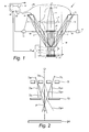
- FIG. 2 schematically shows the operation of an embodiment of the beamlet blanker array 9 in the lithography system of FIG. 1 .
- FIG. 2 schematically shows a cross-sectional view of a portion of a beamlet modulator comprising a beamlet blanker array 9 and beamlet stop array 10.
- the beamlet blanker array 9 is provided with a plurality of apertures.
- the target 24 has also been indicated. The figure is not drawn to scale.
- the shown portion of the beamlet modulator is arranged to modulate three beamlets 7a, 7b, and 7c.
- the beamlets 7a, 7b, 7c may form part of a single group of beamlets that may be generated from a beam originating from a single source or from a single subbeam.
- the beamlet modulator of FIG. 2 is arranged for converging groups of beamlets towards a common point of convergence P for each group. This common point of convergence P is preferably located on an optical axis O for the group of beamlets.
- beamlets 7a, 7b, 7c have an incident angle extending between the beamlet and the optical axis O.
- the orientation of beamlet 7b is substantially parallel to the optical axis.
- the direction of beamlet deflection to establish blocking of deflected beamlets by the substrate of the beamlet stop array 10 may be different for each beamlet.
- Beamlet 7a is blocked by deflection towards the left, i.e. towards the "-"-direction in FIG. 2 , indicated by dashed line 7a-.
- Beamlets 7b, 7c on the other hand are to be deflected towards the right, i.e. towards the "+"-direction, to established blocking of the respective beamlets.
- dashed lines 7b+ and 7c+ These blocking directions are indicated by dashed lines 7b+ and 7c+ respectively. Note that the choice of deflection direction may not be arbitrary. For example, for beamlet 7a, dashed line 7a+ shows that deflection of beamlet 7a towards the right would result in passage through the beamlet stop array 10. Therefore, deflection of beamlet 7a along line 7a+ would be inappropriate. On the other hand, deflection of beamlet 7b towards the left, indicated by dashed line 7b-, would be an option.
- FIG. 3A schematically shows a cross-sectional view of a portion of a beamlet blanker array 9 that may be used in the lithography system of FIG. 1 .
- the beamlet blanker array 9 comprises a plurality of modulators 101.
- a modulator comprises a first electrode 103a, a second electrode 103b, and an aperture 105.
- the electrodes 103a, 103b are located on opposing sides of the aperture 105 for generating an electric field across the aperture.
- a light sensitive element 107 is arranged to receive pattern data carrying light beams (not shown).
- the light sensitive element 107 is electrically connected to one or more modulators 101 via an electrical connection 109.
- the light sensitive element 107 receives pattern data via the light beams, converts the light signal into an electrical signal and then forwards the received and converted pattern data via the electrical connection 109 towards the one or more connected modulators 101.
- the one or more modulators 101 then modulate passing charged particle beamlets, such as electron beamlets 7 in accordance with the received pattern data.
- the light sensitive element 107 may be provided with an anti-reflection coating 108 to reduce background radiation caused by reflected light, which may disturb a correct readout of the data carried by the light beam.
- Modulation of the beamlets is thus based on controlling the application of an electric field across the apertures within the beamlet blanker array 9.
- practical use of a lithography system such as the one presented in FIG. 1 shows that effective modulation is not always possible.
- the light sensitive elements 107 may act as electric field sources due to a collection of scattered electrons on their surface. This may particularly be the case if a anti-reflection coating such as coating 108 in FIGS. 3A, 3B is used.
- the anti-reflection coating is generally electrically insulating, which results in a relatively fast collection of scattered charged particles.
- components that are used to transfer the light towards the light sensitive elements for example optical fibers, may collect charged particles as well, in particular if they are not completely coated with a conductive coating.
- FIG. 3B schematically shows a cross-sectional view of a portion of a beamlet blanker array 9 provided with a shielding structure 111 according to an embodiment of the invention.
- the shielding structure 111 is an electrically conductive structure, and is arranged to shield electric fields and/or magnetic fields generated in proximity of the light sensitive elements 107, for example on top of an electrically insulating layer that may cover the light sensitive elements 107 for protection and/or anti-reflection purposes, from the modulators 105.
- references to the expression "electric field” should be understood to mean electric and/or magnetic field.
- the shielding structure 111 reduces, and preferably eliminates, the interfering of additional electric fields with the fields generated by the modulators 101.
- the reduction or elimination of electric field interference results in more accurate and robust modulation of the charged particle beamlets 7 by the modulators 101.
- the shielding structure 111 is kept at a predetermined electric potential.
- the shielding structure 111 is connected to ground potential.
- the shielding structure is not necessarily in contact with the beamlet blanker array 9.
- the purpose of the shielding structure 111 is to stop the electric fields generated in proximity of the light sensitive elements 107. Note that a fixed connection of the shielding structure 111 with the beamlet blanker array 9 is not essential to achieve such purpose.
- FIG. 3C schematically shows a cross-sectional view of a portion of the blanker array of FIG. 3B .
- FIG. 3C illustrates the ratio between the height h of the shielding structure 111 and the distance d between a light sensitive element 107 and the perpendicular projection of the shielding structure 111 onto the beamlet blanker array 9.
- the distance d will hereinafter be referred to as lateral shielding distance.
- the height h is at least about the same as the lateral shielding distance d.
- Such dimensions allow to effectively shield the electric fields generated in proximity of the light sensitive elements.
- the height h is more than about 2.5 times the lateral shielding distance d , the influence of electric fields generated in proximity of the light sensitive elements on the operation of the modulators is negligible.
- FIG. 4 schematically shows a top view of a lay-out of a beamlet blanker array 9 that may be used in embodiments of the invention.
- the beamlet blanker array 9 shown in FIG. 4 is divided into beam areas 121 and non-beam areas 122. Although the width of the beam areas 121 and non-beam areas 122 are shown to be about the same, this is not essential. The dimensions of the areas may differ based on the layout used.
- the beam areas 121 include one or more modulators for modulating beamlets.
- the non-beam areas 122 include one or more light sensitive elements.
- the use of beam areas 121 and non-beam areas 122 in an optical column in a maskless lithography system has the advantage that the density of modulators and light sensitive area can be increased.
- FIG. 5 schematically shows the beamlet blanker array of FIG. 4 provided with a shielding structure 111 according to an embodiment of the invention.
- the shielding structure 111 that is at least its projection in a direction substantially perpendicular to the beamlet blanker array surface, is located between the light sensitive elements within the non-beam areas 122 and the modulators within the beam areas 121.
- the shielding structure 111 is arranged to substantially shield electric fields generated in proximity of the light sensitive elements.
- the shielding structure 111 of FIG. 5 can be described as comprising side walls forming an open-ended box-like structure.
- the side walls may be integrated into a single body, for example by connection to an additional structure 111'.
- a single body has the benefit of an increased mechanical robustness.
- the structure 111, 111' may be handled more easily. Integration of different components to form the shielding structure 111, 111' may be executed by adding the portions 111' to the separate walls forming the functional shielding structure 111, for example by welding. Alternatively, the shielding structure may be manufactured out of one piece, for example by using techniques such as electrical discharge machining. Yet another way of creating an integrated shielding structure 111, 111' is to attach different components to a supporting substrate. This substrate may be the beamlet blanker array 9 or a component thereof, but may also be a separate suitable substrate.
- the shielding structure 111 is not necessarily physically connected to the beamlet blanker array 9. If located within sufficiently close distance of the beamlet blanker array 9 the shielding structure 111 can still sufficiently shield electric fields.
- the shielding structure 111 further includes a portion 111'.
- This additional portion 111' can provide mechanical support to the shielding structure 111.
- the additional portion 111' is arranged to shield electric and/or magnetic fields originating from other potentially disturbing electric field generating sources, such as electricity cables.
- Materials suitable for the shielding structure 111 are materials with sufficiently high electric conductivity. Additionally, the material should have sufficient strength and workability.
- An exemplary suitable material for use as main component of the shielding structure is titanium (Ti).
- Other exemplary materials that may be used include molybdenum (Mo) and aluminum (Al).
- the shielding structure is made using Ti-plates coated with Mo.
- the shielding structure includes a stack of Mo sheets with Al spacers.
- light beams may be directed towards the light sensitive elements by using an optical fiber array.
- FIG. 6A schematically shows an exemplary embodiment of an optical fiber arrangement 131 selectively placed over the beamlet blanker array 9 of FIG. 5 .
- the optical fiber arrangement 131 comprises a plurality of optical fibers 133 arranged to guide pattern data carrying light beams towards the light sensitive elements within the non-beam areas 122.
- the fibers 133 are positioned such that they do not hinder a passage of charged particle beamlets arranged to pass through the apertures within the beam area 121 of the beamlet blanker array 9.
- the exemplary optical fiber arrangement 131 of FIG. 6A comprises two portions per non-beam area 122.
- a first portion 131a comprises a number of fibers 133 that enter a space above the non-beam area 122 from one side, while the second portion 131b comprises a number of fibers 133 entering the space above the non-beam area 122 at an opposing side.
- the number of fibers 133 within each portion 131a, 131b may be equal to each other.
- the use of different portions allows for more space per fiber 133, and reduces the risk of damaging the fibers 133.
- FIG. 6B schematically shows a cross-sectional view of the arrangement shown in FIG. 6A along the line VIB-VIB'.
- the fibers 133 within the arrangement 131 terminate in a fiber array 135.
- the ends of the fibers within the fiber array 135 are directed towards the light sensitive elements (not shown) within the non-beam area of the beamlet blanker array 9.
- the fiber array 135 is preferably placed in close proximity of the surface of the beamlet blanker array 9 to minimize alignment errors due to poorly oriented fibers 133 within the fiber array 135.
- one or more small openings 137 in the wall 111' are provided to allow the introduction of the fibers within this enclosure.
- the cross-sectional area of these openings 137 is preferably as small as possible.
- the use of portions may help to reduce the dimensions of the cross-sectional area in a direction substantially perpendicular to the surface of the fiber array.
- the cross-sectional area of the openings 137 may be chosen somewhat larger.
- FIG. 6C schematically shows a more detailed view of alignment of the optical fiber arrangement of FIGS. 6A, 6B .
- the fibers 133 within the fiber array 135 are substantially aligned with corresponding light sensitive elements 107 located in the non-beam area of the beamlet blanker array 9.
- the fiber array 135 includes an array of microlenses 139.
- the use of microlenses 139 improves optical communication.
- the microlenses 139 are arranged to focus light leaving the respective fibers 133 onto the light sensitive element 107.
- the microlenses 139 thus reduce the spot size of the light beam at the light receiving surface of the light sensitive element 107.
- the use of microlenses alleviates alignment requirements between fiber array 135 and the light sensitive elements 107. A small deviation of the reduced spot size can still be handled by the light sensitive element because most, if not all, light leaving the respective fiber 133 still falls onto its light receiving surface.
- the fiber array 135 may be placed in close proximity of the light sensitive elements 107 to achieve communication with reduced light loss.
- Such embodiment has the advantage that it is less complex due to the absence of the microlenses 139.
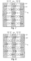
- FIG. 7 schematically shows a top view of a topographic arrangement of a beamlet blanker array according to an embodiment of the invention.
- the beamlet blanker array 9 is again divided in beam areas 121 and non-beam areas 122.
- the beam areas 121 and the non-beam areas 122 are separated by walls forming a shielding structure 111 as discussed earlier.
- the beam areas 121 comprise a plurality of modulators 101.
- the non-beam areas 122 comprise a plurality of light sensitive elements 107. Suitable examples of the light sensitive elements 107 include but are not limited to photodiodes and phototransistors.
- the non-beam areas 122 further include demultiplexers 140.
- the light signals received by the light sensitive elements 107 are multiplexed signals which include information for more than one modulator 101.
- a signal received by a light sensitive element 107 is transferred to a demultiplexer 140.
- the demultiplexer 140 demultiplexes the signal and forwards demultiplexed signals to the correct modulators 101 via dedicated electrical connections 142.
- the number of light sensitive elements 107 is lower than the number of modulators 101. Having a limited number of light sensitive elements 107 enables reduction of the dimensions of the non-beam areas 122.
- the beam areas 121 may then be placed more closely together to increase the number of modulators 101 per unit area in the blanker array 9. In comparison to a non-multiplexed embodiment the layout of the beamlet blanker array 9 would then be more compact if the same number of modulators 101 would be used. If the dimensions of the blanker array 9 would remain substantially the same, more modulators could be used.
- the use of a multiplexed embodiment as shown in FIG. 7 could enable the use of light sensitive elements 107 with a greater light receiving area.
- the use of a greater light receiving area per light sensitive element 107 reduces the complexity of the optics needed to direct the light signal towards the correct light sensitive elements 107 and may alleviate requirements related to the alignment of light beams and light sensitive elements 107.
- FIG. 8 schematically shows a top view of a topographic arrangement of a beamlet blanker array 9 according to an example.
- the shielding structure 111 now embraces a portion of the light sensitive elements 107 and the demultiplexers 142 within a non-beam area 122.
- This modular approach has the advantage that malfunctioning channels and/or components like demultiplexers 142 can be more easily corrected for.
- FIG. 9 schematically shows a top view of a topographic arrangement of a beamlet blanker array 9 according to yet another example.
- the shielding structure 111 now merely embraces the light sensitive elements 107 within a non-beam area 122.
- FIG. 10 schematically shows a cross-sectional view of a beamlet blanker array 9 with an embodiment of a shielding structure 111 using free space optics.
- the light beams 141 indicated herein with dashed-dotted arrows have an incident angle of approximately 90 degrees. Note that this is not essential.
- the particular embodiment of the shielding structure 111 shown in FIG. 10 includes a substrate 160 provided with side walls 161 extending thereon.
- the side walls 161 are located adjacent to apertures 165 within the substrate 160 that are aligned with one or more apertures 105 within the beamlets blanker array 9. Note that although the beamlets 7 in FIG. 10 pass the beamlet array 9 substantially perpendicular, this is not essential.
- the side walls 161 are suitably made of conductive material.
- a side wall 161 is arranged circumferentially around an aperture 165.
- a side wall 161 is arranged circumferentially around a lateral area defined by the one or more light sensitive elements 107.
- a structure of side walls 161 may be provided, including a side wall extending around the lateral area of light sensitive elements and a side wall extending around the aperture 165.
- the shielding structure 111 does not have to be sealed to the beamlet blanker array 9.
- the embodiment of the shielding structure 111 is in particular suitable for a topographical arrangement as schematically shown in FIG. 7 .
- the long extension of the side walls in one direction (in FIG. 7 a vertical direction), height requirements of the shielding structure 111 do not have a significant effect on the angle at which the data carrying light beams can be directed onto the light sensitive elements 107.
- the height of the shielding structure is substantially greater than the lateral shielding distance introducing the light from directions with a significant component substantially perpendicular to the direction of the walls forming the shielding structure limits the angle at which light can reach the light sensitive elements 107.
- the long extension of the shielded area in the direction of the side walls forming the shielding structure 111 now ensures that such limited possible entry of light beams only occurs if the beams originate from a direction with a significant component substantially perpendicular to the side wall orientation.
- the angles at which light can couple into the shielded area when incident from a direction substantially parallel to the side wall orientation may vary widely as no significant shielding is needed in these directions.
- the shielding structure 111 does not necessarily be physically connected to the beamlet blanker array 9. However, in some embodiments both structures are connected.
- FIG. 11 shows an embodiment in which the shielding structure 111 is connected to the blanker array 9 using solder balls 170.
- the solder balls 170 may extend through a passivation layer (not shown) that is commonly used in IC manufacturing.
- the use of such soldering connection may be particularly suitable for shielding structures 111 that embrace a relatively small area, for example in a topographical arrangements as shown in FIGS. 8 and 9 .
- the shielding structure 111 is a wall-like structure having a height that is at least similar in dimensions to the lateral shielding distance.
- a shielding structure 111 comprising a plate 171 with apertures 175.
- Some apertures are aligned with the apertures 105 within the beamlet blanker array 9 while others are aligned with the light sensitive elements 107 to allow illumination of these elements by the data carrying light beams (not shown).
- the embodiment shown in FIG. 11 includes a beamlet blanker array 9 provided with an interconnect structure 173 arranged to enable connection of light sensitive elements 107 at different levels with the electrostatic deflectors 103a, 103b of the modulators 105.
- Such multi-level connection structure may reduce the modulator pitch within the beamlet blanker array 9, which can result in a more compact design.
- the plate 171 may be physically connected to the beamlet blanker array 9, for example via solder balls 170, but may also be positioned at some distance, indicated in FIG. 11 by structure 171' provided with dashed contour lines. In such case, the beamlet blanker array 9 and the structure 171' may be connected to the same frame to ensure that both structures are suitably aligned with respect to each other.
- the distance between the structure 171' and the blanker array 9 may be suitably designed based on the desired extent of electric field shielding and the available angle for data carrying light beams to "hit" the light sensitive elements 107.
- the plate 171, 171' may be a metal piece in which the apertures are shaped by punching.
- An example of such piece is referred to in the semiconductor industry as a leadframe.
- the plate 171, 171' may take the form of a semiconductor or ceramic substrate provided with through-holes, for example made by using one or more suitable etching techniques.
- the direction of the charged particle beamlet 7 is not essential.
- the embodiment shown in FIG. 11 may also be used while a particle beamlet 7 passes through the aperture 105 in a substantially upward direction.
- Fig. 12 shows yet another beamlet blanker array 9 provided with a shielding structure 111.
- the beamlet blanker array 9 of this example comprises a first substrate 200 and a second substrate 201.
- the modulators with deflectors 103a, 103b are defined on the first substrate 200.
- the light sensitive elements 107 are defined at a surface of the second substrate 201.
- Solder balls 202 provide mechanical connections from the first substrate 200 to the second substrate 201 and electrical connections between the light sensitive elements 107 and the deflectors 103a, 103b, and/or any intermediate circuitry.
- Light beams 141 now arrive at the light sensitive elements 107 from an opposite direction, e.g. the top side of the column. Thereto, radiation apertures 205 are present in the first substrate 200.
- the shielding structure 111 is connected to the second substrate 201, and takes the form of side walls.
- the side walls may extend in a single direction (see e.g. topographic arrangement of FIG. 7 ) or may embrace one or more light sensitive elements 107 (see e.g. topographic arrangements of FIGS. 8 and 9 ).
Landscapes
- Chemical & Material Sciences (AREA)
- Engineering & Computer Science (AREA)
- Analytical Chemistry (AREA)
- Nanotechnology (AREA)
- Physics & Mathematics (AREA)
- Crystallography & Structural Chemistry (AREA)
- Condensed Matter Physics & Semiconductors (AREA)
- General Physics & Mathematics (AREA)
- Manufacturing & Machinery (AREA)
- Mathematical Physics (AREA)
- Theoretical Computer Science (AREA)
- Electron Beam Exposure (AREA)
Description
- The invention relates to a modulation device for use in a charged particle multi-beamlet lithography system. The invention further relates to a charged-particle multi-beamlet lithography system. Finally, the invention relates to a method of modulating charged particle beamlets in a charged-particle multi-beamlet lithography system for transferring a pattern to a target surface.
- Charged particle multi-beamlet systems are known in the art, for example from
US-patent 6,958,804 in the name of the applicant (corresponding to US patent applicationUS2004/0135983 ). Such lithography system uses a plurality of charged particle beamlets to transfer a pattern to a target surface. The system may operate with a continuous radiation source or with a source operating at constant frequency. Pattern data are sent to a modulation device arranged to modulate the beamlets by electrostatic deflection. The modulated beamlets are then transferred to the target surface. Generally, during this transfer the diameter of the individual beamlets is reduced. Furthermore, the position of the beamlets with respect to the target surface changes over time, for example due to electrostatic scanning of beamlets and/or movement of the target surface relative to the optical column through which the beamlets are transferred with respect to each other. For example, such relative movement may be established by mechanical movement using a stage provided with a support structure for holding the target. In order to enable a high speed transfer of the pattern to the target surface, optical transmission of pattern data from the control unit to the modulators may be used, for example by using light beams. The modulation device may then include light sensitive elements capable of converting received light signals into corresponding electric signals. - Patterning with a system as described above may suffer from inconsistent pattern transfer due to perturbated modulation of the beamlets. Experiments have shown that the extent of such perturbation is highly unpredictable. As a result, pattern transfer onto a target surface using such system is less reliable than desired,
-
US 2003/0183778 discloses a electron beam exposure apparatus comprising a screening section. - It is therefore an object of the present invention to improve the reliability of pattern transfer onto a target surface using a charged particle multi-beamlet lithography system. This object has been achieved by providing a charged-particle multi-beamlet lithography according to
claim 13. - The present invention is based on the insight that shielding electric and/or magnetic fields originating from charged particle source in the vicinity of the light sensitive elements greatly reduce possible distortions and lead to an improved performance of charged particle lithography.
- The invention further relates to a modulation device according to
claim 1. - The invention further relates to a method of modulating charged particle beamlets in a charged-particle multi-beamlet lithography system according to
claim 14. In this way, the beamlet modulation is carried out using an electric field substantially free of contributions generated in proximity to the light sensitive elements. - Various aspects of the invention will be further explained with reference to embodiments shown in the drawings wherein:
-
FIG. 1 schematically shows a maskless lithography system that may be used in embodiments of the inventions; -
FIG. 2 schematically shows the operation of an embodiment of the beamlet blanker array in the lithography system ofFIG. 1 ; -
FIG. 3A schematically shows a cross-sectional view of a portion of a beamlet blanker array that may be used in the lithography system ofFIG. 1 ; -
FIG. 3B schematically shows a cross-sectional view of a portion of a beamlet blanker array provided with a shielding structure according to an embodiment of the invention; -
FIG. 3C schematically shows a cross-sectional view of a portion of the blanker array ofFIG. 3B ; -
FIG. 4 schematically shows a top view of a lay-out of a beamlet blanker array that may be used in embodiments of the invention; -
FIG. 5 schematically shows the beamlet blanker array ofFIG. 3 provided with a shielding structure according to an embodiment of the invention; -
FIG. 6A schematically shows an optical fiber arrangement on top of the beamlet blanker array ofFIG. 5 ; -
FIG. 6B schematically shows a cross-sectional view of the arrangement shown inFIG. 6A along the line VIB-VIB'; -
FIG. 6C schematically shows a more detailed view of the alignment of the optical fiber arrangement ofFIGS. 6A, 6B ; -
FIG. 7 schematically shows a top view of a topographic arrangement of a beamlet blanker array according to an embodiment of the invention; -
FIG. 8 schematically shows a top view of a topographic arrangement of a beamlet blanker array according an example; and -
FIG. 9 schematically shows a top view of a topographic arrangement of a beamlet blanker array according to yet another example; -
FIG. 10 schematically shows a cross-sectional view of a beamlet blanker array with an embodiment of a shielding structure; -
FIG. 11 schematically shows a cross-sectional view of a beamlet blanker array with an embodiment of a shielding structure; and -
Fig. 12 schematically shows yet another beamlet blanker array provided with a shielding structure. - The following is a description of various embodiments of the invention, given by way of example only and with reference to the figures. The figures are not drawn to scale and merely intended for illustrative purposes.
-
Fig. 1 shows a simplified schematic drawing of an embodiment of a charged particlemulti-beamlet lithography system 1. Such lithography system is for example described inU.S. patent Nos. 6,897,458 and6, 958,804 and7.084,414 and7,129,502 , which are assigned to the applicant of the present application. -
Such lithography system 1 suitably comprises a beamlet generator generating a plurality of beamlets, a beamlet modulator patterning the beamlets to form modulated beamlets, and a beamlet projector for projecting the modulated beamlets onto a surface of a target. - The beamlet generator typically comprises a source and at least one beam splitter. The source in
FIG. 1 is anelectron source 3 arranged to produce a substantially homogeneous, expanding electron beam 4. The beam energy of the electron beam 4 is preferably maintained relatively low in the range of about 1 to 10 keV. To achieve this, the acceleration voltage is preferably low, and theelectron source 3 may be kept at a voltage between about -1 to -10 kV with respect to the target at ground potential, although other settings may also be used. - In
FIG. 1 the electron beam 4 from theelectron source 3 passes a collimator lens 5 for collimating the electron beam 4. The collimator lens 5 may be any type of collimating optical system. Before collimation, the electron beam 4 may pass a double octopole (not shown). Subsequently, the electron beam 4 impinges on a beam splitter, in the embodiment ofFIG. 1 an aperture array 6. The aperture array 6 preferably comprises a plate having through-holes. The aperture array 6 is arranged to block part of the beam 4. Additionally, the array 6 allows a plurality ofbeamlets 7 to pass through so as to produce a plurality ofparallel electron beamlets 7. - The
lithography system 1 ofFIG. 1 generates a large number ofbeamlets 7, preferably about 10,000 to 1,000,000 beamlets, although it is of course possible that more or less beamlets are generated. Note that other known methods may also be used to generate collimated beamlets. A second aperture array may be added in the system, so as to create subbeams from the electron beam 4 and to createelectron beamlets 7 from the subbeam. This allows for manipulation of the subbeams further downstream, which turns out beneficial for the system operation, particularly when the number of beamlets in the system is 5,000 or more. - The beamlet modulator, denoted in
FIG. 1 as modulation system 8, typically comprises a beamletblanker array 9 comprising an arrangement of a plurality of blankers, and abeamlet stop array 10. The blankers are capable of deflecting one or more of theelectron beamlets 7. In embodiments of the invention, the blankers are more specifically electrostatic deflectors provided with a first electrode, a second electrode and an aperture. The electrodes are then located on opposing sides of the aperture for generating an electric field across the aperture. Generally, the second electrode is a ground electrode, i.e. an electrode connected to ground potential. - To focus the
electron beamlets 7 within the plane of theblanker array 9 the lithography system may further comprise a condenser lens array (not shown). - In the embodiment of
FIG. 1 , thebeamlet stop array 10 comprises an array of apertures for allowing beamlets to pass through. Thebeamlet stop array 10, in its basic form, comprises a substrate provided with through-holes, typically round holes although other shapes may also be used. In some embodiments, the substrate of thebeamlet stop array 10 is formed from a silicon wafer with a regularly spaced array of through-holes, and may be coated with a surface layer of a metal to prevent surface charging. In some further embodiments, the metal is of a type that does not form a native-oxide skin, such as CrMo. - The beamlet blanker
array 9 and thebeamlet stop array 10 operate together to block or let pass thebeamlets 7. In some embodiments, the apertures of thebeamlet stop array 10 are aligned with the apertures of the electrostatic deflectors in thebeamlet blanker array 9. If beamletblanker array 9 deflects a beamlet, it will not pass through the corresponding aperture in thebeamlet stop array 10. Instead the beamlet will be blocked by the substrate ofbeamlet block array 10. If beamletblanker array 9 does not deflect a beamlet, the beamlet will pass through the corresponding aperture in thebeamlet stop array 10. In some alternative embodiments, cooperation between the beamletblanker array 9 and thebeamlet stop array 10 is such that deflection of a beamlet by a deflector in theblanker array 9 results in passage of the beamlet through the corresponding aperture in thebeamlet stop array 10, while non-deflection results in blockage by the substrate of thebeamlet stop array 10. - The modulation system 8 is arranged to add a pattern to the
beamlets 7 on the basis of input provided by acontrol unit 60. Thecontrol unit 60 may comprise adata storage unit 61, a read outunit 62 anddata converter 63. Thecontrol unit 60 may be located remote from the rest of the system, for instance outside the inner part of a clean room. Usingoptical fibers 64, modulated light beams 14 holding pattern data may be transmitted to aprojector 65 which projects light from the ends of fibers within a fiber array (schematically depicted as plate 15) into the electron optical portion of thelithography system 1, schematically denoted by the dashed box andreference number 18. - In the embodiment of
FIG. 1 , the modulated light beams are projected on to thebeamlet blanker array 9. More particularly, the modulated light beams 14 from optical fiber ends are projected on corresponding light sensitive elements located on thebeamlet blanker array 9. The light sensitive elements may be arranged to convert the light signal into a different type of signal, for example an electric signal. A modulatedlight beam 14 carries a portion of the pattern data for controlling one or more blankers that are coupled to a corresponding light sensitive element. Suitably, in order to project the light beams 14 onto corresponding light sensitive elements optical elements such as aprojector 65 may be used. Additionally, to allow projection of the light beams 14 at a suitable incident angle, a mirror may be included, for example suitably placed between aprojector 65 and the beamlet blankerarray 9. Theprojector 65 may be appropriately aligned with theplate 15 by aprojector positioning device 17 under control of thecontrol unit 60. As a result, the distance between theprojector 65 and the light sensitive elements within the light sensitive element may vary as well. - In some embodiments, the light beams may, at least partially, be transferred from the plate towards the light sensitive elements by means of an optical waveguide. The optical waveguide may guide the light to a position very close to the light sensitive elements, suitably less than a centimeter, preferably in the order of a millimeter away. A short distance between an optical waveguide and a corresponding light sensitive elements reduces light loss. On the other hand, the use of
plate 15 and aprojector 65 located away from the space that may be occupied by the charged particle beamlets has the advantage that the beamlet disturbance is minimized, and the construction of the beamlet blankerarray 9 is less complex. - The modulated beamlets coming out of the beamlet modulator are projected as a spot onto a
target surface 13 of atarget 24 by the beamlet projector. The beamlet projector typically comprises a scanning deflector for scanning the modulated beamlets over thetarget surface 13 and a projection lens system for focusing the modulated beamlets onto thetarget surface 13. These components may be present within a single end module. - Such end module is preferably constructed as an insertable, replaceable unit. The end module may thus comprise a
deflector array 11, and aprojection lens arrangement 12. The insertable, replaceable unit may also include thebeamlet stop array 10 as discussed above with reference to the beamlet modulator. After leaving the end module, thebeamlets 7 impinge on atarget surface 13 positioned at a target plane. For lithography applications, the target usually comprises a wafer provided with a charged-particle sensitive layer or resist layer. - The
deflector array 11 may take the form of a scanning deflector array arranged to deflect eachbeamlet 7 that passed thebeamlet stop array 10. Thedeflector array 11 may comprise a plurality of electrostatic deflectors enabling the application of relatively small driving voltages. Although thedeflector array 11 is drawn upstream of theprojection lens arrangement 12, thedeflector array 11 may also be positioned between theprojection lens arrangement 12 and thetarget surface 13. - The
projection lens arrangement 12 is arranged to focus thebeamlets 7, before or after deflection by thedeflector array 11. Preferably, the focusing results a geometric spot size of about 10 to 30 nanometers in diameter. In such preferred embodiment, theprojection lens arrangement 12 is preferably arranged to provide a demagnification of about 100 to 500 times, most preferably as large as possible, e.g. in the range 300 to 500 times. In this preferred embodiment, theprojection lens arrangement 12 may be advantageously located close to thetarget surface 13. - In some embodiments, a beam protector (not shown) may be located between the
target surface 13 and theprojection lens arrangement 12. The beam protector may be a foil or a plate provided with a plurality of suitably positioned apertures. The beam protector is arranged to absorb the released resist particles before they can reach any of the sensitive elements in thelithography system 1. - The
projection lens arrangement 12 may thus ensure that the spot size of a single pixel on thetarget surface 13 is correct, while thedeflector array 11 may ensure by appropriate scanning operations that the position of a pixel on thetarget surface 13 is correct on a microscale. Particularly, the operation of thedeflector array 11 is such that a pixel fits into a grid of pixels which ultimately constitutes the pattern on thetarget surface 13. It will be understood that the macroscale positioning of the pixel on thetarget surface 13 is suitably enabled by a wafer positioning system present below thetarget 24. - Commonly, the
target surface 13 comprises a resist film on top of a substrate. Portions of the resist film will be chemically modified by application of the beamlets of charged particles, i.e. electrons. As a result thereof, the irradiated portion of the film will be more or less soluble in a developer, resulting in a resist pattern on a wafer. The resist pattern on the wafer can subsequently be transferred to an underlying layer, i.e. by implementation, etching and/or deposition steps as known in the art of semiconductor manufacturing. Evidently, if the irradiation is not uniform, the resist may not be developed in a uniform manner, leading to mistakes in the pattern. High-quality projection is therefore relevant to obtain a lithography system that provides a reproducible result. No difference in irradiation ought to result from deflection steps. -
FIG. 2 schematically shows the operation of an embodiment of the beamlet blankerarray 9 in the lithography system ofFIG. 1 . In particular,FIG. 2 schematically shows a cross-sectional view of a portion of a beamlet modulator comprising abeamlet blanker array 9 andbeamlet stop array 10. The beamlet blankerarray 9 is provided with a plurality of apertures. For sake of reference thetarget 24 has also been indicated. The figure is not drawn to scale. - The shown portion of the beamlet modulator is arranged to modulate three
beamlets beamlets FIG. 2 is arranged for converging groups of beamlets towards a common point of convergence P for each group. This common point of convergence P is preferably located on an optical axis O for the group of beamlets. - Considering the shown beamlets 7a, 7b, 7c in
FIG. 2 ,beamlets beamlet 7b is substantially parallel to the optical axis. The direction of beamlet deflection to establish blocking of deflected beamlets by the substrate of thebeamlet stop array 10 may be different for each beamlet.Beamlet 7a is blocked by deflection towards the left, i.e. towards the "-"-direction inFIG. 2 , indicated by dashedline 7a-.Beamlets beamlet 7a, dashed line 7a+ shows that deflection ofbeamlet 7a towards the right would result in passage through thebeamlet stop array 10. Therefore, deflection ofbeamlet 7a along line 7a+ would be inappropriate. On the other hand, deflection ofbeamlet 7b towards the left, indicated by dashedline 7b-, would be an option. -
FIG. 3A schematically shows a cross-sectional view of a portion of a beamlet blankerarray 9 that may be used in the lithography system ofFIG. 1 . The beamlet blankerarray 9 comprises a plurality ofmodulators 101. A modulator comprises afirst electrode 103a, asecond electrode 103b, and anaperture 105. Theelectrodes aperture 105 for generating an electric field across the aperture. - A light
sensitive element 107 is arranged to receive pattern data carrying light beams (not shown). The lightsensitive element 107 is electrically connected to one ormore modulators 101 via anelectrical connection 109. The lightsensitive element 107 receives pattern data via the light beams, converts the light signal into an electrical signal and then forwards the received and converted pattern data via theelectrical connection 109 towards the one or moreconnected modulators 101. The one ormore modulators 101 then modulate passing charged particle beamlets, such as electron beamlets 7 in accordance with the received pattern data. The lightsensitive element 107 may be provided with ananti-reflection coating 108 to reduce background radiation caused by reflected light, which may disturb a correct readout of the data carried by the light beam. - Modulation of the beamlets is thus based on controlling the application of an electric field across the apertures within the beamlet blanker
array 9. However, practical use of a lithography system such as the one presented inFIG. 1 shows that effective modulation is not always possible. It turns out that the lightsensitive elements 107 may act as electric field sources due to a collection of scattered electrons on their surface. This may particularly be the case if a anti-reflection coating such ascoating 108 inFIGS. 3A, 3B is used. The anti-reflection coating is generally electrically insulating, which results in a relatively fast collection of scattered charged particles. Additionally, components that are used to transfer the light towards the light sensitive elements, for example optical fibers, may collect charged particles as well, in particular if they are not completely coated with a conductive coating. - The strength of electric fields caused by local collection of scattered charged particles generally depends on statistical parameters and other uncontrollable actors. Therefore, it is very difficult to predict how large the fields will be and where they will be located exactly. Experiments have shown that electric fields originating from a collection of scattered electrons can have a significant influence on position of a charged particle beamlet. This means that the beamlet position can be unstable. Furthermore, the extent of charged particle beamlet deflection may become unpredictable as well. As a result, the patterned beamlets obtained by modulation with the beamlet blanker array may not transfer a pattern that corresponds with the pattern provided to the
beamlet blanker array 9 via the pattern data carrying light beams. -
FIG. 3B schematically shows a cross-sectional view of a portion of a beamlet blankerarray 9 provided with a shieldingstructure 111 according to an embodiment of the invention. The shieldingstructure 111 is an electrically conductive structure, and is arranged to shield electric fields and/or magnetic fields generated in proximity of the lightsensitive elements 107, for example on top of an electrically insulating layer that may cover the lightsensitive elements 107 for protection and/or anti-reflection purposes, from themodulators 105. In the remainder of this specification references to the expression "electric field" should be understood to mean electric and/or magnetic field. - The shielding
structure 111 reduces, and preferably eliminates, the interfering of additional electric fields with the fields generated by themodulators 101. The reduction or elimination of electric field interference results in more accurate and robust modulation of the chargedparticle beamlets 7 by themodulators 101. The shieldingstructure 111 is kept at a predetermined electric potential. Preferably, the shieldingstructure 111 is connected to ground potential. - As can be seen in
FIG. 3B , the shielding structure is not necessarily in contact with the beamlet blankerarray 9. The purpose of the shieldingstructure 111 is to stop the electric fields generated in proximity of the lightsensitive elements 107. Note that a fixed connection of the shieldingstructure 111 with the beamlet blankerarray 9 is not essential to achieve such purpose. -
FIG. 3C schematically shows a cross-sectional view of a portion of the blanker array ofFIG. 3B . In particular,FIG. 3C illustrates the ratio between the height h of the shieldingstructure 111 and the distance d between a lightsensitive element 107 and the perpendicular projection of the shieldingstructure 111 onto the beamlet blankerarray 9. The distance d will hereinafter be referred to as lateral shielding distance. Preferably, the height h is at least about the same as the lateral shielding distance d. Such dimensions allow to effectively shield the electric fields generated in proximity of the light sensitive elements. In particular if the height h is more than about 2.5 times the lateral shielding distance d, the influence of electric fields generated in proximity of the light sensitive elements on the operation of the modulators is negligible. -
FIG. 4 schematically shows a top view of a lay-out of a beamlet blankerarray 9 that may be used in embodiments of the invention. The beamlet blankerarray 9 shown inFIG. 4 is divided intobeam areas 121 andnon-beam areas 122. Although the width of thebeam areas 121 andnon-beam areas 122 are shown to be about the same, this is not essential. The dimensions of the areas may differ based on the layout used. - The
beam areas 121 include one or more modulators for modulating beamlets. Thenon-beam areas 122 include one or more light sensitive elements. The use ofbeam areas 121 andnon-beam areas 122 in an optical column in a maskless lithography system has the advantage that the density of modulators and light sensitive area can be increased. -
FIG. 5 schematically shows the beamlet blanker array ofFIG. 4 provided with a shieldingstructure 111 according to an embodiment of the invention. The shieldingstructure 111, that is at least its projection in a direction substantially perpendicular to the beamlet blanker array surface, is located between the light sensitive elements within thenon-beam areas 122 and the modulators within thebeam areas 121. The shieldingstructure 111 is arranged to substantially shield electric fields generated in proximity of the light sensitive elements. - The shielding
structure 111 ofFIG. 5 can be described as comprising side walls forming an open-ended box-like structure. The side walls may be integrated into a single body, for example by connection to an additional structure 111'. A single body has the benefit of an increased mechanical robustness. Furthermore, thestructure 111, 111' may be handled more easily. Integration of different components to form the shieldingstructure 111, 111' may be executed by adding the portions 111' to the separate walls forming thefunctional shielding structure 111, for example by welding. Alternatively, the shielding structure may be manufactured out of one piece, for example by using techniques such as electrical discharge machining. Yet another way of creating anintegrated shielding structure 111, 111' is to attach different components to a supporting substrate. This substrate may be the beamlet blankerarray 9 or a component thereof, but may also be a separate suitable substrate. - The shielding
structure 111 is not necessarily physically connected to thebeamlet blanker array 9. If located within sufficiently close distance of the beamlet blankerarray 9 the shieldingstructure 111 can still sufficiently shield electric fields. - In the embodiment shown in
FIG. 5 , the shieldingstructure 111 further includes a portion 111'. This additional portion 111' can provide mechanical support to the shieldingstructure 111. In some embodiments, the additional portion 111' is arranged to shield electric and/or magnetic fields originating from other potentially disturbing electric field generating sources, such as electricity cables. - Materials suitable for the shielding
structure 111 are materials with sufficiently high electric conductivity. Additionally, the material should have sufficient strength and workability. An exemplary suitable material for use as main component of the shielding structure is titanium (Ti). Other exemplary materials that may be used include molybdenum (Mo) and aluminum (Al). In an exemplary embodiment, the shielding structure is made using Ti-plates coated with Mo. In another exemplary embodiment the shielding structure includes a stack of Mo sheets with Al spacers. - As discussed with reference to
FIG. 1 , light beams may be directed towards the light sensitive elements by using an optical fiber array. In some embodiments, it is advantageous to keep the distance between the fiber array and the light sensitive elements relatively short to reduce light losses. -
FIG. 6A schematically shows an exemplary embodiment of anoptical fiber arrangement 131 selectively placed over the beamletblanker array 9 ofFIG. 5 . Theoptical fiber arrangement 131 comprises a plurality ofoptical fibers 133 arranged to guide pattern data carrying light beams towards the light sensitive elements within thenon-beam areas 122. Thefibers 133 are positioned such that they do not hinder a passage of charged particle beamlets arranged to pass through the apertures within thebeam area 121 of the beamlet blankerarray 9. - The exemplary
optical fiber arrangement 131 ofFIG. 6A comprises two portions pernon-beam area 122. Afirst portion 131a comprises a number offibers 133 that enter a space above thenon-beam area 122 from one side, while thesecond portion 131b comprises a number offibers 133 entering the space above thenon-beam area 122 at an opposing side. The number offibers 133 within eachportion fiber 133, and reduces the risk of damaging thefibers 133. -
FIG. 6B schematically shows a cross-sectional view of the arrangement shown inFIG. 6A along the line VIB-VIB'. Thefibers 133 within thearrangement 131 terminate in afiber array 135. The ends of the fibers within thefiber array 135 are directed towards the light sensitive elements (not shown) within the non-beam area of the beamlet blankerarray 9. Thefiber array 135 is preferably placed in close proximity of the surface of the beamlet blankerarray 9 to minimize alignment errors due to poorly orientedfibers 133 within thefiber array 135. - The use of a complete enclosure embracing the non-beam area provides an effective shield for electric fields originating from locations within the non-beam area. As can be seen in
FIG. 6B , in this embodiment one or moresmall openings 137 in the wall 111' are provided to allow the introduction of the fibers within this enclosure. For shielding reasons, the cross-sectional area of theseopenings 137 is preferably as small as possible. The use of portions may help to reduce the dimensions of the cross-sectional area in a direction substantially perpendicular to the surface of the fiber array. However, to avoid damage to the fibers due to friction and/or strain the cross-sectional area of theopenings 137 may be chosen somewhat larger. -
FIG. 6C schematically shows a more detailed view of alignment of the optical fiber arrangement ofFIGS. 6A, 6B . As can be seen inFIG. 6C , thefibers 133 within thefiber array 135 are substantially aligned with corresponding lightsensitive elements 107 located in the non-beam area of the beamlet blankerarray 9. - In the embodiment shown in
FIG. 6C , thefiber array 135 includes an array ofmicrolenses 139. The use ofmicrolenses 139 improves optical communication. Themicrolenses 139 are arranged to focus light leaving therespective fibers 133 onto the lightsensitive element 107. Themicrolenses 139 thus reduce the spot size of the light beam at the light receiving surface of the lightsensitive element 107. The use of microlenses alleviates alignment requirements betweenfiber array 135 and the lightsensitive elements 107. A small deviation of the reduced spot size can still be handled by the light sensitive element because most, if not all, light leaving therespective fiber 133 still falls onto its light receiving surface. - Instead of using
microlenses 139 thefiber array 135 may be placed in close proximity of the lightsensitive elements 107 to achieve communication with reduced light loss. Such embodiment has the advantage that it is less complex due to the absence of themicrolenses 139. -
FIG. 7 schematically shows a top view of a topographic arrangement of a beamlet blanker array according to an embodiment of the invention. The beamlet blankerarray 9 is again divided inbeam areas 121 andnon-beam areas 122. InFIG. 7 , thebeam areas 121 and thenon-beam areas 122 are separated by walls forming a shieldingstructure 111 as discussed earlier. - The
beam areas 121 comprise a plurality ofmodulators 101. Thenon-beam areas 122 comprise a plurality of lightsensitive elements 107. Suitable examples of the lightsensitive elements 107 include but are not limited to photodiodes and phototransistors. - The
non-beam areas 122 further includedemultiplexers 140. In this embodiment, the light signals received by the lightsensitive elements 107 are multiplexed signals which include information for more than onemodulator 101. A signal received by a lightsensitive element 107 is transferred to ademultiplexer 140. Thedemultiplexer 140 demultiplexes the signal and forwards demultiplexed signals to thecorrect modulators 101 via dedicatedelectrical connections 142. - As a result of multiplexed light signals,
demultiplexers 140 and demultiplexed electrical signals, the number of lightsensitive elements 107 is lower than the number ofmodulators 101. Having a limited number of lightsensitive elements 107 enables reduction of the dimensions of thenon-beam areas 122. Thebeam areas 121 may then be placed more closely together to increase the number ofmodulators 101 per unit area in theblanker array 9. In comparison to a non-multiplexed embodiment the layout of the beamlet blankerarray 9 would then be more compact if the same number ofmodulators 101 would be used. If the dimensions of theblanker array 9 would remain substantially the same, more modulators could be used. Alternatively, instead of decreasing the size of thenon-beam areas 122 the use of a multiplexed embodiment as shown inFIG. 7 could enable the use of lightsensitive elements 107 with a greater light receiving area. The use of a greater light receiving area per lightsensitive element 107 reduces the complexity of the optics needed to direct the light signal towards the correct lightsensitive elements 107 and may alleviate requirements related to the alignment of light beams and lightsensitive elements 107. -
FIG. 8 schematically shows a top view of a topographic arrangement of a beamlet blankerarray 9 according to an example. In contrast to the embodiment shown inFIG. 7 , the shieldingstructure 111 now embraces a portion of the lightsensitive elements 107 and thedemultiplexers 142 within anon-beam area 122. This modular approach has the advantage that malfunctioning channels and/or components likedemultiplexers 142 can be more easily corrected for. -
FIG. 9 schematically shows a top view of a topographic arrangement of a beamlet blankerarray 9 according to yet another example. In contrast to the embodiment shown inFIG. 8 , the shieldingstructure 111 now merely embraces the lightsensitive elements 107 within anon-beam area 122. - Note that, although the preceding embodiments and examples , in particular the embodiments described with reference to
FIGS. 6A-6C , were directed to transfer of pattern data carrying light beams towards a location in proximity of the light sensitive elements via optical fibers, it may be equally possible to use free space optics, in particular in the area close to the beamlet blanker array. The use of free space optics has the advantage that no space needs to be reserved for the accommodation of fibers. Furthermore, different light paths may be created by using optical elements like mirrors. The use of optical elements in free space optics increases the flexibility of forming light paths. The mechanical limitations of optical fibers, for example a limited ability to bend in a small space, play no role. -
FIG. 10 schematically shows a cross-sectional view of a beamlet blankerarray 9 with an embodiment of a shieldingstructure 111 using free space optics. The light beams 141, indicated herein with dashed-dotted arrows have an incident angle of approximately 90 degrees. Note that this is not essential. - The particular embodiment of the shielding
structure 111 shown inFIG. 10 includes asubstrate 160 provided withside walls 161 extending thereon. Theside walls 161 are located adjacent toapertures 165 within thesubstrate 160 that are aligned with one ormore apertures 105 within the beamlets blankerarray 9. Note that although thebeamlets 7 inFIG. 10 pass thebeamlet array 9 substantially perpendicular, this is not essential. - The
side walls 161 are suitably made of conductive material. In some examples, aside wall 161 is arranged circumferentially around anaperture 165. In some other examples, aside wall 161 is arranged circumferentially around a lateral area defined by the one or more lightsensitive elements 107. In such case, a structure ofside walls 161 may be provided, including a side wall extending around the lateral area of light sensitive elements and a side wall extending around theaperture 165. The shieldingstructure 111 does not have to be sealed to thebeamlet blanker array 9. - The embodiment of the shielding
structure 111 is in particular suitable for a topographical arrangement as schematically shown inFIG. 7 . The long extension of the side walls in one direction (inFIG. 7 a vertical direction), height requirements of the shieldingstructure 111 do not have a significant effect on the angle at which the data carrying light beams can be directed onto the lightsensitive elements 107. In particular, if a design is used where the height of the shielding structure is substantially greater than the lateral shielding distance introducing the light from directions with a significant component substantially perpendicular to the direction of the walls forming the shielding structure limits the angle at which light can reach the lightsensitive elements 107. - The long extension of the shielded area in the direction of the side walls forming the shielding
structure 111 now ensures that such limited possible entry of light beams only occurs if the beams originate from a direction with a significant component substantially perpendicular to the side wall orientation. The angles at which light can couple into the shielded area when incident from a direction substantially parallel to the side wall orientation may vary widely as no significant shielding is needed in these directions. - As mentioned earlier, the shielding
structure 111 does not necessarily be physically connected to thebeamlet blanker array 9. However, in some embodiments both structures are connected. For example,FIG. 11 shows an embodiment in which theshielding structure 111 is connected to theblanker array 9 usingsolder balls 170. Thesolder balls 170 may extend through a passivation layer (not shown) that is commonly used in IC manufacturing. The use of such soldering connection may be particularly suitable for shieldingstructures 111 that embrace a relatively small area, for example in a topographical arrangements as shown inFIGS. 8 and9 . - Furthermore, in the embodiments and examples shown above, the shielding
structure 111 is a wall-like structure having a height that is at least similar in dimensions to the lateral shielding distance. However, in some applications is may be sufficient to use ashielding structure 111 comprising aplate 171 withapertures 175. Some apertures are aligned with theapertures 105 within the beamlet blankerarray 9 while others are aligned with the lightsensitive elements 107 to allow illumination of these elements by the data carrying light beams (not shown). - The embodiment shown in
FIG. 11 includes a beamletblanker array 9 provided with aninterconnect structure 173 arranged to enable connection of lightsensitive elements 107 at different levels with theelectrostatic deflectors modulators 105. Such multi-level connection structure may reduce the modulator pitch within the beamlet blankerarray 9, which can result in a more compact design. - The
plate 171 may be physically connected to thebeamlet blanker array 9, for example viasolder balls 170, but may also be positioned at some distance, indicated inFIG. 11 bystructure 171' provided with dashed contour lines. In such case, the beamlet blankerarray 9 and thestructure 171' may be connected to the same frame to ensure that both structures are suitably aligned with respect to each other. The distance between thestructure 171' and theblanker array 9 may be suitably designed based on the desired extent of electric field shielding and the available angle for data carrying light beams to "hit" the lightsensitive elements 107. - The
plate plate - Note that the direction of the charged
particle beamlet 7 is not essential. The embodiment shown inFIG. 11 may also be used while aparticle beamlet 7 passes through theaperture 105 in a substantially upward direction. -
Fig. 12 shows yet another beamlet blankerarray 9 provided with a shieldingstructure 111. The beamlet blankerarray 9 of this example comprises a first substrate 200 and asecond substrate 201. The modulators withdeflectors sensitive elements 107 are defined at a surface of thesecond substrate 201.Solder balls 202 provide mechanical connections from the first substrate 200 to thesecond substrate 201 and electrical connections between the lightsensitive elements 107 and thedeflectors Light beams 141 now arrive at the lightsensitive elements 107 from an opposite direction, e.g. the top side of the column. Thereto,radiation apertures 205 are present in the first substrate 200. In the shown example the shieldingstructure 111 is connected to thesecond substrate 201, and takes the form of side walls. The side walls may extend in a single direction (see e.g. topographic arrangement ofFIG. 7 ) or may embrace one or more light sensitive elements 107 (see e.g. topographic arrangements ofFIGS. 8 and9 ). - The invention has been described by reference to certain embodiments discussed above. These embodiments are not limiting upon the scope of the invention, which is defined in the accompanying claims.
Claims (14)
- A modulation device (8) for use in a charged-particle multi-beamlet lithography system (1), the modulation device (8) comprising:- a beamlet blanker array (9) for patterning a plurality of beamlets (7) in accordance with a pattern, wherein the beamlet blanker array (9) comprises a plurality of modulators (101) and a plurality of light sensitive elements (107), the light sensitive elements (107) being arranged to receive pattern data carrying light beams (14, 141) and to convert the light beams into electrical signals, the light sensitive element (107) being electrically connected to one or more modulators (101) for providing the received pattern data to the one or more modulators (101);wherein the beamlet blanker array (9) comprises a substrate provided with a first area (121) comprising at least one modulator (101) and a second area (122) free of modulators and including one or more light sensitive elements (107); characterized in that the modulation device further comprises- a shielding structure (111) of an electrically conductive material arranged to substantially shield electric fields generated in proximity of the light sensitive elements (107) from the modulators (101), wherein the shielding structure (111) is arranged to be set at a predetermined potential;and in that the projection of the shielding structure (111) onto the beamlet blanker array (9) forms a boundary between the first and second areas, thereby shielding the modulators from electric fields generated in the proximity of the light sensitive elements.
- The device of claim 1, wherein a modulator of the plurality of modulators (101) comprises a first electrode (103a), a second electrode (103b) and an aperture (105), the electrodes being located on opposing sides of the aperture (105) for generating an electric field across the aperture (105).
- The device of claim 2, wherein the first area (121) and the second area (122) take the form of adjacent strips, and the shielding structure (111) comprises a wall having a length and a height, and a projection of the shielding structure (111) onto the substrate surface of the beamlet blanker array (9) in a direction substantially parallel to the wall height and substantially perpendicular to the wall length separates the first area (121) from the second area (122).
- The device of any one of claims 1-3, wherein the shielding structure (111) comprises side walls forming an open-ended box-like structure.
- The device of claim 4, wherein a first end of the open-ended box-like structure faces towards the substrate surface of the beamlet blanker array (9) and an opposing second end of the open-ended box like structure faces away from the beamlet blanker array (9).
- The device of claim 5, wherein the second end is provided with a lid substantially closing the second end.
- The device of any one of claims 4-6, wherein the volume embraced by the shielding structure comprises one or more optical elements for guiding the pattern data carrying light beams (14, 141) to the light sensitive elements (107).
- The device of claim 7, wherein the one or more optical elements comprise an array of optical fibers (135).
- The device of any one of claims 4 - 8, wherein at least one of the side walls is arranged for introducing the pattern data carrying light beams (14, 141) into the volume embraced by the shielding structure (111).
- The device of claim 9, wherein at least one of the side walls of the shielding structure (111) comprises an opening for accommodating entry of optical fibers (133) into the volume embraced by the shielding structure (111).
- The device of claim 9, wherein at least one of the side walls of the shielding structure (111) comprises a portion that is transparent for light of the pattern data carrying light beams (14, 141).
- The device of any one of claims 4 - 11, wherein the ratio between the height of the shielding structure (111) and the distance between a light sensitive element (107) and the perpendicular projection of the closest side wall of the shielding structure (111) onto the beamlet blanker array (9) is greater than about 1, preferably greater than about 2.5.
- A charged-particle multi-beamlet lithography system (1) for transferring a pattern onto the surface of a target (13) using a plurality of charged particle beamlets, the system comprising:- a beam generator (3,4,5) for generating a plurality of charged particle beamlets (7);- a modulation device (8) according to any one of claims 1 - 12; and- a projection system (12) for projecting the patterned beamlets onto the target surface (13).
- A method of modulating charged particle beamlets (7) in a charged-particle multi-beamlet lithography system (1) for transferring a pattern to a target surface (13), the method comprising:- providing a beamlet blanker array (9) comprising a plurality of modulators (101) and a plurality of light sensitive elements (107), the light sensitive elements (107) being arranged to receive pattern data carrying light beams (14, 141) and being electrically connected to one or more modulators for providing the received pattern data, and the modulators comprising a first electrode (103 a), a second electrode (103b) and an aperture (105), wherein the electrodes are located on opposing sides of the apertures for generating an electric field across the aperture (105),
said beamlet blanker array (9) further comprising a shielding structure (111) of an electrically conductive material for substantially shielding electric fields generated by the modulators for modulating the beamlets from electric fields generated in proximity of the light sensitive elements (107), wherein the shielding structure (111) is arranged to be set at a predetermined potential,
and wherein the beamlet blanker array (9) comprises a substrate provided with a first area (121) comprising at least one modulator (101) and a second area (122) free of modulators and including one or more light sensitive elements (107), and wherein the projection of the shielding structure (111) onto the beamlet blanker array (9) forms a boundary between the first and second areas;
transmitting a pattern data to the beamlet blanker array;
and- modulating beamlets passing through the beamlet blanker array in accordance with the received pattern data,wherein the beamlet modulation is carried out using an electric field substantially free of contributions generated in proximity of the light sensitive elements (107).
Applications Claiming Priority (2)
| Application Number | Priority Date | Filing Date | Title |
|---|---|---|---|
| US25477909P | 2009-10-26 | 2009-10-26 | |
| PCT/EP2010/066198 WO2011051304A1 (en) | 2009-10-26 | 2010-10-26 | Modulation device and charged particle multi-beamlet lithography system using the same |
Publications (2)
| Publication Number | Publication Date |
|---|---|
| EP2494580A1 EP2494580A1 (en) | 2012-09-05 |
| EP2494580B1 true EP2494580B1 (en) | 2016-10-19 |
Family
ID=43500320
Family Applications (3)
| Application Number | Title | Priority Date | Filing Date |
|---|---|---|---|
| EP10773891.6A Active EP2494580B1 (en) | 2009-10-26 | 2010-10-26 | Modulation device and charged particle multi-beamlet lithography system using the same |
| EP10773617.5A Active EP2494579B1 (en) | 2009-10-26 | 2010-10-26 | Charged particle multi-beamlet lithography system, modulation device, and method of manufacturing thereof |
| EP10773044.2A Active EP2494578B1 (en) | 2009-10-26 | 2010-10-26 | Charged particle multi-beamlet lithography system, with modulation device |
Family Applications After (2)
| Application Number | Title | Priority Date | Filing Date |
|---|---|---|---|
| EP10773617.5A Active EP2494579B1 (en) | 2009-10-26 | 2010-10-26 | Charged particle multi-beamlet lithography system, modulation device, and method of manufacturing thereof |
| EP10773044.2A Active EP2494578B1 (en) | 2009-10-26 | 2010-10-26 | Charged particle multi-beamlet lithography system, with modulation device |
Country Status (8)
| Country | Link |
|---|---|
| US (4) | US8841636B2 (en) |
| EP (3) | EP2494580B1 (en) |
| JP (3) | JP5844269B2 (en) |
| KR (3) | KR20120098756A (en) |
| CN (3) | CN102668015B (en) |
| NL (2) | NL2005583C2 (en) |
| TW (2) | TWI498937B (en) |
| WO (3) | WO2011051304A1 (en) |
Families Citing this family (37)
| Publication number | Priority date | Publication date | Assignee | Title |
|---|---|---|---|---|
| US8258484B2 (en) * | 2008-04-15 | 2012-09-04 | Mapper Lithography Ip B.V. | Beamlet blanker arrangement |
| US9341936B2 (en) | 2008-09-01 | 2016-05-17 | D2S, Inc. | Method and system for forming a pattern on a reticle using charged particle beam lithography |
| JP5844269B2 (en) * | 2009-10-26 | 2016-01-13 | マッパー・リソグラフィー・アイピー・ビー.ブイ. | Charged particle multiple beamlet lithography system with adjustment device |
| US8921758B2 (en) * | 2010-10-26 | 2014-12-30 | Mapper Lithography Ip B.V. | Modulation device and charged particle multi-beamlet lithography system using the same |
| JP5679774B2 (en) * | 2010-11-09 | 2015-03-04 | キヤノン株式会社 | Deflector array, charged particle drawing apparatus, device manufacturing method, and deflector array manufacturing method |
| NL2007604C2 (en) * | 2011-10-14 | 2013-05-01 | Mapper Lithography Ip Bv | Charged particle system comprising a manipulator device for manipulation of one or more charged particle beams. |
| NL2006868C2 (en) * | 2011-05-30 | 2012-12-03 | Mapper Lithography Ip Bv | Charged particle multi-beamlet apparatus. |
| US8719739B2 (en) | 2011-09-19 | 2014-05-06 | D2S, Inc. | Method and system for forming patterns using charged particle beam lithography |
| JP2013182945A (en) * | 2012-02-29 | 2013-09-12 | Canon Inc | Lithography device and product manufacturing method |
| WO2013142068A1 (en) * | 2012-03-19 | 2013-09-26 | Kla-Tencor Corporation | Pillar-supported array of micro electron lenses |
| US9343267B2 (en) | 2012-04-18 | 2016-05-17 | D2S, Inc. | Method and system for dimensional uniformity using charged particle beam lithography |
| NL2010759C2 (en) | 2012-05-14 | 2015-08-25 | Mapper Lithography Ip Bv | Modulation device and power supply arrangement. |
| JP2014007013A (en) * | 2012-06-22 | 2014-01-16 | Canon Inc | Electrostatic lens array, multiple charged particle optical system and focus adjusting method |
| WO2015090378A1 (en) * | 2013-12-18 | 2015-06-25 | Mapper Lithography Ip Bv | Modulation device and lithography system comprising such device |
| JP5816739B1 (en) * | 2014-12-02 | 2015-11-18 | 株式会社ニューフレアテクノロジー | Multi-beam blanking aperture array device and method for manufacturing multi-beam blanking aperture array device |
| JP6426489B2 (en) * | 2015-02-03 | 2018-11-21 | 東京エレクトロン株式会社 | Etching method |
| JP2017168574A (en) * | 2016-03-15 | 2017-09-21 | 株式会社ニューフレアテクノロジー | Multi charged particle beam blanking apparatus, multi charged particle beam blanking method, and multi charged particle beam writing apparatus |
| US9981293B2 (en) | 2016-04-21 | 2018-05-29 | Mapper Lithography Ip B.V. | Method and system for the removal and/or avoidance of contamination in charged particle beam systems |
| NL2019503B1 (en) | 2016-09-08 | 2018-08-31 | Mapper Lithography Ip Bv | Fabricating unique chips using a charged particle multi-beamlet lithography system |
| US10522472B2 (en) | 2016-09-08 | 2019-12-31 | Asml Netherlands B.V. | Secure chips with serial numbers |
| US10418324B2 (en) | 2016-10-27 | 2019-09-17 | Asml Netherlands B.V. | Fabricating unique chips using a charged particle multi-beamlet lithography system |
| EP3559752A4 (en) | 2016-12-23 | 2020-08-19 | ASML Netherlands B.V. | Fabricating unique chips using a charged particle multi-beamlet lithography system |
| JP6720861B2 (en) | 2016-12-28 | 2020-07-08 | 株式会社ニューフレアテクノロジー | Multi-beam aperture set and multi-charged particle beam drawing device |
| US10840056B2 (en) * | 2017-02-03 | 2020-11-17 | Kla Corporation | Multi-column scanning electron microscopy system |
| US11289304B2 (en) | 2017-04-28 | 2022-03-29 | Asml Netherlands B.V. | Apparatus using multiple beams of charged particles |
| JP7286630B2 (en) * | 2017-10-02 | 2023-06-05 | エーエスエムエル ネザーランズ ビー.ブイ. | Equipment using a charged particle beam |
| JP6966958B2 (en) * | 2018-03-01 | 2021-11-17 | 株式会社荏原製作所 | Plating equipment with paddles and paddles used to stir the plating solution |
| JP6847886B2 (en) * | 2018-03-20 | 2021-03-24 | 株式会社東芝 | Charged particle beam deflection device |
| IL277822B2 (en) * | 2018-05-01 | 2024-08-01 | Asml Netherlands Bv | Multi-beam inspection apparatus |
| JP6965222B2 (en) * | 2018-09-14 | 2021-11-10 | 株式会社東芝 | Semiconductor device |
| KR102596926B1 (en) | 2018-12-31 | 2023-11-01 | 에이에스엠엘 네델란즈 비.브이. | multi-beam inspection device |
| DE102019005362A1 (en) * | 2019-07-31 | 2021-02-04 | Carl Zeiss Multisem Gmbh | Method for operating a multitude particle beam system with changing the numerical aperture, associated computer program product and multitude particle beam system |
| US11120965B2 (en) * | 2019-12-04 | 2021-09-14 | ICT Integrated Circuit Testing Gesellschaft für Halbleiterprüftechnik mbH | Beam blanking device for a multi-beamlet charged particle beam apparatus |
| JP7359050B2 (en) * | 2020-03-18 | 2023-10-11 | 株式会社ニューフレアテクノロジー | Multi-beam blanking device and multi-charged particle beam lithography device |
| NL2027746B1 (en) * | 2021-03-12 | 2022-09-29 | Elstar Dynamics Patents B V | Dynamic glazing comprising a substrate with interlaced mesh electrodes |
| KR20240093780A (en) | 2021-10-19 | 2024-06-24 | 에이에스엠엘 네델란즈 비.브이. | Detector assemblies, charged particle devices, apparatus, and methods |
| EP4170695A1 (en) | 2021-10-19 | 2023-04-26 | ASML Netherlands B.V. | Detector assembly, charged particle device, apparatus, and methods |
Family Cites Families (35)
| Publication number | Priority date | Publication date | Assignee | Title |
|---|---|---|---|---|
| JPS554011A (en) * | 1978-06-22 | 1980-01-12 | Nippon Telegr & Teleph Corp <Ntt> | Optical branching and receiving device |
| JP3145149B2 (en) * | 1991-10-17 | 2001-03-12 | 富士通株式会社 | Charged particle beam deflector |
| US5719416A (en) * | 1991-12-13 | 1998-02-17 | Symetrix Corporation | Integrated circuit with layered superlattice material compound |
| DE4241045C1 (en) | 1992-12-05 | 1994-05-26 | Bosch Gmbh Robert | Process for anisotropic etching of silicon |
| GB9316280D0 (en) * | 1993-08-05 | 1993-09-22 | Capteur Sensors & Analysers | Gas sensors |
| JP3311927B2 (en) * | 1996-04-18 | 2002-08-05 | トヨタ自動車株式会社 | Optical-Magneto-optical effect measuring device |
| JP4246401B2 (en) * | 2001-01-18 | 2009-04-02 | 株式会社アドバンテスト | Electron beam exposure apparatus and electron beam deflection apparatus |
| KR100385228B1 (en) * | 2001-04-18 | 2003-05-27 | 삼성전자주식회사 | Method and device of programming nonvolatile memory |
| JP4248191B2 (en) * | 2002-04-10 | 2009-04-02 | キヤノン株式会社 | Method for manufacturing array structure |
| US6818911B2 (en) * | 2002-04-10 | 2004-11-16 | Canon Kabushiki Kaisha | Array structure and method of manufacturing the same, charged particle beam exposure apparatus, and device manufacturing method |
| CN100476599C (en) * | 2002-09-20 | 2009-04-08 | Asml荷兰有限公司 | Photoetching mark structure, photoetching projection device comprising the photoetching mark structure, and method for aligning with the photoetching mark structure |
| EP2302459A3 (en) * | 2002-10-25 | 2011-04-06 | Mapper Lithography Ip B.V. | Lithography system |
| JP5053514B2 (en) | 2002-10-30 | 2012-10-17 | マッパー・リソグラフィー・アイピー・ビー.ブイ. | Electron beam exposure system |
| JP2004282038A (en) | 2003-02-28 | 2004-10-07 | Canon Inc | Deflector, method for producing deflector, and charged particle beam exposure device using deflector |
| WO2004081910A2 (en) | 2003-03-10 | 2004-09-23 | Mapper Lithography Ip B.V. | Apparatus for generating a plurality of beamlets |
| CN100543920C (en) | 2003-05-28 | 2009-09-23 | 迈普尔平版印刷Ip有限公司 | The charged particle beamlet exposure system |
| JP4387755B2 (en) * | 2003-10-14 | 2009-12-24 | キヤノン株式会社 | Deflector array and manufacturing method thereof, and charged particle beam exposure apparatus using the deflector array |
| US7394071B2 (en) * | 2004-12-20 | 2008-07-01 | Electronics And Telecommunications Research Institute | Micro column electron beam apparatus formed in low temperature co-fired ceramic substrate |
| JP4652829B2 (en) * | 2005-01-26 | 2011-03-16 | キヤノン株式会社 | Electron beam exposure apparatus and device manufacturing method |
| US20060204166A1 (en) * | 2005-03-14 | 2006-09-14 | Naugler W E Jr | Method and apparatus for monitoring and calibrating an emissive pixel |
| JP2007019242A (en) * | 2005-07-07 | 2007-01-25 | Canon Inc | Deflector, charged particle beam exposure apparatus, and device manufacturing method |
| JP2007019248A (en) * | 2005-07-07 | 2007-01-25 | Canon Inc | Deflector, electrically-charged particle beam exposure device and device manufacturing method |
| JP4673170B2 (en) * | 2005-09-12 | 2011-04-20 | 株式会社日立ハイテクノロジーズ | Device for multi-electron beam drawing apparatus and manufacturing method thereof |
| DE102008010123A1 (en) * | 2007-02-28 | 2008-09-04 | Ims Nanofabrication Ag | Multibeam deflecting array device for maskless particle beam machining |
| JP5491704B2 (en) | 2007-05-14 | 2014-05-14 | イーエムエス ナノファブリカツィオン アーゲー | Pattern definition device having counter electrode array plate |
| US8258484B2 (en) * | 2008-04-15 | 2012-09-04 | Mapper Lithography Ip B.V. | Beamlet blanker arrangement |
| CN102067271B (en) * | 2008-04-15 | 2014-05-21 | 迈普尔平版印刷Ip有限公司 | Beamlet blanker arrangement |
| GB2459279A (en) | 2008-04-16 | 2009-10-21 | Mapper Lithography B V | A projection system for charged particle multi-beams |
| JP5587299B2 (en) * | 2008-05-23 | 2014-09-10 | マッパー・リソグラフィー・アイピー・ビー.ブイ. | Imaging system |
| ATE527678T1 (en) * | 2008-11-17 | 2011-10-15 | Ims Nanofabrication Ag | METHOD FOR MASKLESS PARTICLE BEAM EXPOSURE |
| US8198601B2 (en) * | 2009-01-28 | 2012-06-12 | Ims Nanofabrication Ag | Method for producing a multi-beam deflector array device having electrodes |
| EP2433295A2 (en) * | 2009-05-20 | 2012-03-28 | Mapper Lithography IP B.V. | Dual pass scanning |
| JP5844269B2 (en) * | 2009-10-26 | 2016-01-13 | マッパー・リソグラフィー・アイピー・ビー.ブイ. | Charged particle multiple beamlet lithography system with adjustment device |
| US8921758B2 (en) * | 2010-10-26 | 2014-12-30 | Mapper Lithography Ip B.V. | Modulation device and charged particle multi-beamlet lithography system using the same |
| US8604411B2 (en) * | 2010-11-13 | 2013-12-10 | Mapper Lithography Ip B.V. | Charged particle beam modulator |
-
2010
- 2010-10-26 JP JP2012535797A patent/JP5844269B2/en active Active
- 2010-10-26 TW TW099136453A patent/TWI498937B/en active
- 2010-10-26 EP EP10773891.6A patent/EP2494580B1/en active Active
- 2010-10-26 EP EP10773617.5A patent/EP2494579B1/en active Active
- 2010-10-26 CN CN201080048345.4A patent/CN102668015B/en active Active
- 2010-10-26 CN CN201080059454.6A patent/CN102687233B/en active Active
- 2010-10-26 JP JP2012535794A patent/JP5781523B2/en active Active
- 2010-10-26 WO PCT/EP2010/066198 patent/WO2011051304A1/en active Application Filing
- 2010-10-26 US US12/911,859 patent/US8841636B2/en active Active
- 2010-10-26 KR KR1020127013929A patent/KR20120098756A/en not_active Application Discontinuation
- 2010-10-26 JP JP2012535796A patent/JP2013508992A/en active Pending
- 2010-10-26 TW TW099136655A patent/TW201142905A/en unknown
- 2010-10-26 EP EP10773044.2A patent/EP2494578B1/en active Active
- 2010-10-26 WO PCT/EP2010/066195 patent/WO2011051301A1/en active Application Filing
- 2010-10-26 CN CN2010800594527A patent/CN102687232A/en active Pending
- 2010-10-26 US US12/911,861 patent/US8987677B2/en active Active
- 2010-10-26 NL NL2005583A patent/NL2005583C2/en not_active IP Right Cessation
- 2010-10-26 KR KR1020127013931A patent/KR20120088780A/en not_active Application Discontinuation
- 2010-10-26 KR KR1020127013930A patent/KR101609347B1/en active IP Right Grant
- 2010-10-26 US US12/911,911 patent/US8492731B2/en active Active
- 2010-10-26 NL NL2005584A patent/NL2005584C2/en not_active IP Right Cessation
- 2010-10-26 WO PCT/EP2010/066199 patent/WO2011051305A1/en active Application Filing
-
2013
- 2013-07-09 US US13/937,321 patent/US8759787B2/en active Active
Also Published As
Similar Documents
| Publication | Publication Date | Title |
|---|---|---|
| EP2494580B1 (en) | Modulation device and charged particle multi-beamlet lithography system using the same | |
| EP2633545B1 (en) | Modulation device and charged particle multi-beamlet lithography system using the same | |
| EP2638559B1 (en) | Charged particle beam modulator | |
| USRE48287E1 (en) | Method for forming an optical fiber array | |
| EP2402979B1 (en) | Projection lens arrangement | |
| US8502176B2 (en) | Imaging system | |
| US20120273690A1 (en) | Charged particle system comprising a manipulator device for manipulation of one or more charged particle beams |
Legal Events
| Date | Code | Title | Description |
|---|---|---|---|
| PUAI | Public reference made under article 153(3) epc to a published international application that has entered the european phase |
Free format text: ORIGINAL CODE: 0009012 |
|
| 17P | Request for examination filed |
Effective date: 20120524 |
|
| AK | Designated contracting states |
Kind code of ref document: A1 Designated state(s): AL AT BE BG CH CY CZ DE DK EE ES FI FR GB GR HR HU IE IS IT LI LT LU LV MC MK MT NL NO PL PT RO RS SE SI SK SM TR |
|
| DAX | Request for extension of the european patent (deleted) | ||
| 17Q | First examination report despatched |
Effective date: 20140625 |
|
| REG | Reference to a national code |
Ref country code: DE Ref legal event code: R079 Ref document number: 602010037344 Country of ref document: DE Free format text: PREVIOUS MAIN CLASS: H01J0037317000 Ipc: H01J0037070000 |
|
| GRAP | Despatch of communication of intention to grant a patent |
Free format text: ORIGINAL CODE: EPIDOSNIGR1 |
|
| RIC1 | Information provided on ipc code assigned before grant |
Ipc: H01J 37/317 20060101ALI20150519BHEP Ipc: H01J 37/04 20060101ALI20150519BHEP Ipc: H01J 37/07 20060101AFI20150519BHEP |
|
| INTG | Intention to grant announced |
Effective date: 20150602 |
|
| GRAP | Despatch of communication of intention to grant a patent |
Free format text: ORIGINAL CODE: EPIDOSNIGR1 |
|
| INTG | Intention to grant announced |
Effective date: 20150825 |
|
| GRAP | Despatch of communication of intention to grant a patent |
Free format text: ORIGINAL CODE: EPIDOSNIGR1 |
|
| RIN1 | Information on inventor provided before grant (corrected) |
Inventor name: JAGER, REMCO Inventor name: STEENBRINK, STIJN WILLEM HERMAN KAREL Inventor name: VAN VEEN, ALEXANDER HENDRIK VINCENT Inventor name: WIELAND, MARCO JAN-JACO |
|
| INTG | Intention to grant announced |
Effective date: 20160502 |
|
| GRAS | Grant fee paid |
Free format text: ORIGINAL CODE: EPIDOSNIGR3 |
|
| GRAA | (expected) grant |
Free format text: ORIGINAL CODE: 0009210 |
|
| AK | Designated contracting states |
Kind code of ref document: B1 Designated state(s): AL AT BE BG CH CY CZ DE DK EE ES FI FR GB GR HR HU IE IS IT LI LT LU LV MC MK MT NL NO PL PT RO RS SE SI SK SM TR |
|
| REG | Reference to a national code |
Ref country code: GB Ref legal event code: FG4D |
|
| REG | Reference to a national code |
Ref country code: CH Ref legal event code: EP |
|
| REG | Reference to a national code |
Ref country code: AT Ref legal event code: REF Ref document number: 838973 Country of ref document: AT Kind code of ref document: T Effective date: 20161115 |
|
| REG | Reference to a national code |
Ref country code: IE Ref legal event code: FG4D |
|
| REG | Reference to a national code |
Ref country code: FR Ref legal event code: PLFP Year of fee payment: 7 |
|
| REG | Reference to a national code |
Ref country code: DE Ref legal event code: R096 Ref document number: 602010037344 Country of ref document: DE |
|
| REG | Reference to a national code |
Ref country code: NL Ref legal event code: FP |
|
| REG | Reference to a national code |
Ref country code: LT Ref legal event code: MG4D |
|
| PG25 | Lapsed in a contracting state [announced via postgrant information from national office to epo] |
Ref country code: LV Free format text: LAPSE BECAUSE OF FAILURE TO SUBMIT A TRANSLATION OF THE DESCRIPTION OR TO PAY THE FEE WITHIN THE PRESCRIBED TIME-LIMIT Effective date: 20161019 Ref country code: BE Free format text: LAPSE BECAUSE OF NON-PAYMENT OF DUE FEES Effective date: 20161031 |
|
| PG25 | Lapsed in a contracting state [announced via postgrant information from national office to epo] |
Ref country code: LT Free format text: LAPSE BECAUSE OF FAILURE TO SUBMIT A TRANSLATION OF THE DESCRIPTION OR TO PAY THE FEE WITHIN THE PRESCRIBED TIME-LIMIT Effective date: 20161019 Ref country code: GR Free format text: LAPSE BECAUSE OF FAILURE TO SUBMIT A TRANSLATION OF THE DESCRIPTION OR TO PAY THE FEE WITHIN THE PRESCRIBED TIME-LIMIT Effective date: 20170120 Ref country code: SE Free format text: LAPSE BECAUSE OF FAILURE TO SUBMIT A TRANSLATION OF THE DESCRIPTION OR TO PAY THE FEE WITHIN THE PRESCRIBED TIME-LIMIT Effective date: 20161019 Ref country code: NO Free format text: LAPSE BECAUSE OF FAILURE TO SUBMIT A TRANSLATION OF THE DESCRIPTION OR TO PAY THE FEE WITHIN THE PRESCRIBED TIME-LIMIT Effective date: 20170119 |
|
| PG25 | Lapsed in a contracting state [announced via postgrant information from national office to epo] |
Ref country code: RS Free format text: LAPSE BECAUSE OF FAILURE TO SUBMIT A TRANSLATION OF THE DESCRIPTION OR TO PAY THE FEE WITHIN THE PRESCRIBED TIME-LIMIT Effective date: 20161019 Ref country code: PL Free format text: LAPSE BECAUSE OF FAILURE TO SUBMIT A TRANSLATION OF THE DESCRIPTION OR TO PAY THE FEE WITHIN THE PRESCRIBED TIME-LIMIT Effective date: 20161019 Ref country code: ES Free format text: LAPSE BECAUSE OF FAILURE TO SUBMIT A TRANSLATION OF THE DESCRIPTION OR TO PAY THE FEE WITHIN THE PRESCRIBED TIME-LIMIT Effective date: 20161019 Ref country code: BE Free format text: LAPSE BECAUSE OF FAILURE TO SUBMIT A TRANSLATION OF THE DESCRIPTION OR TO PAY THE FEE WITHIN THE PRESCRIBED TIME-LIMIT Effective date: 20161019 Ref country code: FI Free format text: LAPSE BECAUSE OF FAILURE TO SUBMIT A TRANSLATION OF THE DESCRIPTION OR TO PAY THE FEE WITHIN THE PRESCRIBED TIME-LIMIT Effective date: 20161019 Ref country code: PT Free format text: LAPSE BECAUSE OF FAILURE TO SUBMIT A TRANSLATION OF THE DESCRIPTION OR TO PAY THE FEE WITHIN THE PRESCRIBED TIME-LIMIT Effective date: 20170220 Ref country code: HR Free format text: LAPSE BECAUSE OF FAILURE TO SUBMIT A TRANSLATION OF THE DESCRIPTION OR TO PAY THE FEE WITHIN THE PRESCRIBED TIME-LIMIT Effective date: 20161019 Ref country code: IS Free format text: LAPSE BECAUSE OF FAILURE TO SUBMIT A TRANSLATION OF THE DESCRIPTION OR TO PAY THE FEE WITHIN THE PRESCRIBED TIME-LIMIT Effective date: 20170219 |
|
| REG | Reference to a national code |
Ref country code: CH Ref legal event code: PL |
|
| REG | Reference to a national code |
Ref country code: DE Ref legal event code: R097 Ref document number: 602010037344 Country of ref document: DE |
|
| PG25 | Lapsed in a contracting state [announced via postgrant information from national office to epo] |
Ref country code: EE Free format text: LAPSE BECAUSE OF FAILURE TO SUBMIT A TRANSLATION OF THE DESCRIPTION OR TO PAY THE FEE WITHIN THE PRESCRIBED TIME-LIMIT Effective date: 20161019 Ref country code: SK Free format text: LAPSE BECAUSE OF FAILURE TO SUBMIT A TRANSLATION OF THE DESCRIPTION OR TO PAY THE FEE WITHIN THE PRESCRIBED TIME-LIMIT Effective date: 20161019 Ref country code: MC Free format text: LAPSE BECAUSE OF FAILURE TO SUBMIT A TRANSLATION OF THE DESCRIPTION OR TO PAY THE FEE WITHIN THE PRESCRIBED TIME-LIMIT Effective date: 20161019 Ref country code: CH Free format text: LAPSE BECAUSE OF NON-PAYMENT OF DUE FEES Effective date: 20161031 Ref country code: CZ Free format text: LAPSE BECAUSE OF FAILURE TO SUBMIT A TRANSLATION OF THE DESCRIPTION OR TO PAY THE FEE WITHIN THE PRESCRIBED TIME-LIMIT Effective date: 20161019 Ref country code: LI Free format text: LAPSE BECAUSE OF NON-PAYMENT OF DUE FEES Effective date: 20161031 Ref country code: DK Free format text: LAPSE BECAUSE OF FAILURE TO SUBMIT A TRANSLATION OF THE DESCRIPTION OR TO PAY THE FEE WITHIN THE PRESCRIBED TIME-LIMIT Effective date: 20161019 Ref country code: RO Free format text: LAPSE BECAUSE OF FAILURE TO SUBMIT A TRANSLATION OF THE DESCRIPTION OR TO PAY THE FEE WITHIN THE PRESCRIBED TIME-LIMIT Effective date: 20161019 |
|
| PLBE | No opposition filed within time limit |
Free format text: ORIGINAL CODE: 0009261 |
|
| STAA | Information on the status of an ep patent application or granted ep patent |
Free format text: STATUS: NO OPPOSITION FILED WITHIN TIME LIMIT |
|
| PG25 | Lapsed in a contracting state [announced via postgrant information from national office to epo] |
Ref country code: LU Free format text: LAPSE BECAUSE OF NON-PAYMENT OF DUE FEES Effective date: 20161026 Ref country code: BG Free format text: LAPSE BECAUSE OF FAILURE TO SUBMIT A TRANSLATION OF THE DESCRIPTION OR TO PAY THE FEE WITHIN THE PRESCRIBED TIME-LIMIT Effective date: 20170119 Ref country code: SM Free format text: LAPSE BECAUSE OF FAILURE TO SUBMIT A TRANSLATION OF THE DESCRIPTION OR TO PAY THE FEE WITHIN THE PRESCRIBED TIME-LIMIT Effective date: 20161019 Ref country code: IT Free format text: LAPSE BECAUSE OF FAILURE TO SUBMIT A TRANSLATION OF THE DESCRIPTION OR TO PAY THE FEE WITHIN THE PRESCRIBED TIME-LIMIT Effective date: 20161019 |
|
| 26N | No opposition filed |
Effective date: 20170720 |
|
| REG | Reference to a national code |
Ref country code: FR Ref legal event code: PLFP Year of fee payment: 8 |
|
| PG25 | Lapsed in a contracting state [announced via postgrant information from national office to epo] |
Ref country code: SI Free format text: LAPSE BECAUSE OF FAILURE TO SUBMIT A TRANSLATION OF THE DESCRIPTION OR TO PAY THE FEE WITHIN THE PRESCRIBED TIME-LIMIT Effective date: 20161019 |
|
| PG25 | Lapsed in a contracting state [announced via postgrant information from national office to epo] |
Ref country code: CY Free format text: LAPSE BECAUSE OF FAILURE TO SUBMIT A TRANSLATION OF THE DESCRIPTION OR TO PAY THE FEE WITHIN THE PRESCRIBED TIME-LIMIT Effective date: 20161019 Ref country code: HU Free format text: LAPSE BECAUSE OF FAILURE TO SUBMIT A TRANSLATION OF THE DESCRIPTION OR TO PAY THE FEE WITHIN THE PRESCRIBED TIME-LIMIT; INVALID AB INITIO Effective date: 20101026 |
|
| PG25 | Lapsed in a contracting state [announced via postgrant information from national office to epo] |
Ref country code: MK Free format text: LAPSE BECAUSE OF FAILURE TO SUBMIT A TRANSLATION OF THE DESCRIPTION OR TO PAY THE FEE WITHIN THE PRESCRIBED TIME-LIMIT Effective date: 20161019 Ref country code: TR Free format text: LAPSE BECAUSE OF FAILURE TO SUBMIT A TRANSLATION OF THE DESCRIPTION OR TO PAY THE FEE WITHIN THE PRESCRIBED TIME-LIMIT Effective date: 20161019 Ref country code: MT Free format text: LAPSE BECAUSE OF NON-PAYMENT OF DUE FEES Effective date: 20161031 |
|
| REG | Reference to a national code |
Ref country code: FR Ref legal event code: PLFP Year of fee payment: 9 |
|
| REG | Reference to a national code |
Ref country code: AT Ref legal event code: UEP Ref document number: 838973 Country of ref document: AT Kind code of ref document: T Effective date: 20161019 |
|
| REG | Reference to a national code |
Ref country code: NL Ref legal event code: PD Owner name: ASML NETHERLANDS B.V.; NL Free format text: DETAILS ASSIGNMENT: CHANGE OF OWNER(S), ASSIGNMENT; FORMER OWNER NAME: MAPPER LITHOGRAPHY IP B.V. Effective date: 20190425 |
|
| PG25 | Lapsed in a contracting state [announced via postgrant information from national office to epo] |
Ref country code: AL Free format text: LAPSE BECAUSE OF FAILURE TO SUBMIT A TRANSLATION OF THE DESCRIPTION OR TO PAY THE FEE WITHIN THE PRESCRIBED TIME-LIMIT Effective date: 20161019 |
|
| PGFP | Annual fee paid to national office [announced via postgrant information from national office to epo] |
Ref country code: FR Payment date: 20221024 Year of fee payment: 13 |
|
| PGFP | Annual fee paid to national office [announced via postgrant information from national office to epo] |
Ref country code: IE Payment date: 20221019 Year of fee payment: 13 Ref country code: GB Payment date: 20221018 Year of fee payment: 13 Ref country code: AT Payment date: 20221019 Year of fee payment: 13 |
|
| P01 | Opt-out of the competence of the unified patent court (upc) registered |
Effective date: 20230403 |
|
| PGFP | Annual fee paid to national office [announced via postgrant information from national office to epo] |
Ref country code: NL Payment date: 20231026 Year of fee payment: 14 |
|
| PGFP | Annual fee paid to national office [announced via postgrant information from national office to epo] |
Ref country code: DE Payment date: 20231027 Year of fee payment: 14 |
|
| REG | Reference to a national code |
Ref country code: AT Ref legal event code: MM01 Ref document number: 838973 Country of ref document: AT Kind code of ref document: T Effective date: 20231026 |
|
| GBPC | Gb: european patent ceased through non-payment of renewal fee |
Effective date: 20231026 |
|
| PG25 | Lapsed in a contracting state [announced via postgrant information from national office to epo] |
Ref country code: GB Free format text: LAPSE BECAUSE OF NON-PAYMENT OF DUE FEES Effective date: 20231026 |
|
| PG25 | Lapsed in a contracting state [announced via postgrant information from national office to epo] |
Ref country code: AT Free format text: LAPSE BECAUSE OF NON-PAYMENT OF DUE FEES Effective date: 20231026 |
|
| PG25 | Lapsed in a contracting state [announced via postgrant information from national office to epo] |
Ref country code: GB Free format text: LAPSE BECAUSE OF NON-PAYMENT OF DUE FEES Effective date: 20231026 Ref country code: FR Free format text: LAPSE BECAUSE OF NON-PAYMENT OF DUE FEES Effective date: 20231031 Ref country code: AT Free format text: LAPSE BECAUSE OF NON-PAYMENT OF DUE FEES Effective date: 20231026 |