JP2004282017A - Positioning system and method for lithographic apparatus - Google Patents
Positioning system and method for lithographic apparatus Download PDFInfo
- Publication number
- JP2004282017A JP2004282017A JP2003366657A JP2003366657A JP2004282017A JP 2004282017 A JP2004282017 A JP 2004282017A JP 2003366657 A JP2003366657 A JP 2003366657A JP 2003366657 A JP2003366657 A JP 2003366657A JP 2004282017 A JP2004282017 A JP 2004282017A
- Authority
- JP
- Japan
- Prior art keywords
- target
- positioning
- positioning mark
- detector
- signal
- Prior art date
- Legal status (The legal status is an assumption and is not a legal conclusion. Google has not performed a legal analysis and makes no representation as to the accuracy of the status listed.)
- Pending
Links
Images


Classifications
-
- G—PHYSICS
- G03—PHOTOGRAPHY; CINEMATOGRAPHY; ANALOGOUS TECHNIQUES USING WAVES OTHER THAN OPTICAL WAVES; ELECTROGRAPHY; HOLOGRAPHY
- G03F—PHOTOMECHANICAL PRODUCTION OF TEXTURED OR PATTERNED SURFACES, e.g. FOR PRINTING, FOR PROCESSING OF SEMICONDUCTOR DEVICES; MATERIALS THEREFOR; ORIGINALS THEREFOR; APPARATUS SPECIALLY ADAPTED THEREFOR
- G03F9/00—Registration or positioning of originals, masks, frames, photographic sheets or textured or patterned surfaces, e.g. automatically
- G03F9/70—Registration or positioning of originals, masks, frames, photographic sheets or textured or patterned surfaces, e.g. automatically for microlithography
- G03F9/7073—Alignment marks and their environment
- G03F9/7084—Position of mark on substrate, i.e. position in (x, y, z) of mark, e.g. buried or resist covered mark, mark on rearside, at the substrate edge, in the circuit area, latent image mark, marks in plural levels
-
- G—PHYSICS
- G03—PHOTOGRAPHY; CINEMATOGRAPHY; ANALOGOUS TECHNIQUES USING WAVES OTHER THAN OPTICAL WAVES; ELECTROGRAPHY; HOLOGRAPHY
- G03F—PHOTOMECHANICAL PRODUCTION OF TEXTURED OR PATTERNED SURFACES, e.g. FOR PRINTING, FOR PROCESSING OF SEMICONDUCTOR DEVICES; MATERIALS THEREFOR; ORIGINALS THEREFOR; APPARATUS SPECIALLY ADAPTED THEREFOR
- G03F9/00—Registration or positioning of originals, masks, frames, photographic sheets or textured or patterned surfaces, e.g. automatically
- G03F9/70—Registration or positioning of originals, masks, frames, photographic sheets or textured or patterned surfaces, e.g. automatically for microlithography
- G03F9/7003—Alignment type or strategy, e.g. leveling, global alignment
- G03F9/7046—Strategy, e.g. mark, sensor or wavelength selection
-
- G—PHYSICS
- G03—PHOTOGRAPHY; CINEMATOGRAPHY; ANALOGOUS TECHNIQUES USING WAVES OTHER THAN OPTICAL WAVES; ELECTROGRAPHY; HOLOGRAPHY
- G03F—PHOTOMECHANICAL PRODUCTION OF TEXTURED OR PATTERNED SURFACES, e.g. FOR PRINTING, FOR PROCESSING OF SEMICONDUCTOR DEVICES; MATERIALS THEREFOR; ORIGINALS THEREFOR; APPARATUS SPECIALLY ADAPTED THEREFOR
- G03F9/00—Registration or positioning of originals, masks, frames, photographic sheets or textured or patterned surfaces, e.g. automatically
- G03F9/70—Registration or positioning of originals, masks, frames, photographic sheets or textured or patterned surfaces, e.g. automatically for microlithography
- G03F9/7049—Technique, e.g. interferometric
-
- G—PHYSICS
- G03—PHOTOGRAPHY; CINEMATOGRAPHY; ANALOGOUS TECHNIQUES USING WAVES OTHER THAN OPTICAL WAVES; ELECTROGRAPHY; HOLOGRAPHY
- G03F—PHOTOMECHANICAL PRODUCTION OF TEXTURED OR PATTERNED SURFACES, e.g. FOR PRINTING, FOR PROCESSING OF SEMICONDUCTOR DEVICES; MATERIALS THEREFOR; ORIGINALS THEREFOR; APPARATUS SPECIALLY ADAPTED THEREFOR
- G03F9/00—Registration or positioning of originals, masks, frames, photographic sheets or textured or patterned surfaces, e.g. automatically
- G03F9/70—Registration or positioning of originals, masks, frames, photographic sheets or textured or patterned surfaces, e.g. automatically for microlithography
- G03F9/7065—Production of alignment light, e.g. light source, control of coherence, polarization, pulse length, wavelength
-
- G—PHYSICS
- G03—PHOTOGRAPHY; CINEMATOGRAPHY; ANALOGOUS TECHNIQUES USING WAVES OTHER THAN OPTICAL WAVES; ELECTROGRAPHY; HOLOGRAPHY
- G03F—PHOTOMECHANICAL PRODUCTION OF TEXTURED OR PATTERNED SURFACES, e.g. FOR PRINTING, FOR PROCESSING OF SEMICONDUCTOR DEVICES; MATERIALS THEREFOR; ORIGINALS THEREFOR; APPARATUS SPECIALLY ADAPTED THEREFOR
- G03F9/00—Registration or positioning of originals, masks, frames, photographic sheets or textured or patterned surfaces, e.g. automatically
- G03F9/70—Registration or positioning of originals, masks, frames, photographic sheets or textured or patterned surfaces, e.g. automatically for microlithography
- G03F9/7073—Alignment marks and their environment
- G03F9/7076—Mark details, e.g. phase grating mark, temporary mark
-
- G—PHYSICS
- G03—PHOTOGRAPHY; CINEMATOGRAPHY; ANALOGOUS TECHNIQUES USING WAVES OTHER THAN OPTICAL WAVES; ELECTROGRAPHY; HOLOGRAPHY
- G03F—PHOTOMECHANICAL PRODUCTION OF TEXTURED OR PATTERNED SURFACES, e.g. FOR PRINTING, FOR PROCESSING OF SEMICONDUCTOR DEVICES; MATERIALS THEREFOR; ORIGINALS THEREFOR; APPARATUS SPECIALLY ADAPTED THEREFOR
- G03F9/00—Registration or positioning of originals, masks, frames, photographic sheets or textured or patterned surfaces, e.g. automatically
- G03F9/70—Registration or positioning of originals, masks, frames, photographic sheets or textured or patterned surfaces, e.g. automatically for microlithography
- G03F9/7088—Alignment mark detection, e.g. TTR, TTL, off-axis detection, array detector, video detection
-
- G—PHYSICS
- G03—PHOTOGRAPHY; CINEMATOGRAPHY; ANALOGOUS TECHNIQUES USING WAVES OTHER THAN OPTICAL WAVES; ELECTROGRAPHY; HOLOGRAPHY
- G03F—PHOTOMECHANICAL PRODUCTION OF TEXTURED OR PATTERNED SURFACES, e.g. FOR PRINTING, FOR PROCESSING OF SEMICONDUCTOR DEVICES; MATERIALS THEREFOR; ORIGINALS THEREFOR; APPARATUS SPECIALLY ADAPTED THEREFOR
- G03F9/00—Registration or positioning of originals, masks, frames, photographic sheets or textured or patterned surfaces, e.g. automatically
- G03F9/70—Registration or positioning of originals, masks, frames, photographic sheets or textured or patterned surfaces, e.g. automatically for microlithography
- G03F9/7092—Signal processing
Abstract
Description
本発明はリソグラフィ投影装置の位置決めシステム、およびこのような位置決めシステムを有するリソグラフィ投影装置に係り、特にほぼ並列に検出される少なくとも2つの独立した信号を使用した位置決めマークの位置検出および/または多ターゲット・マークの位置検出を可能にする位置決めシステムに関するものである。 The present invention relates to a positioning system for a lithographic projection apparatus, and to a lithographic projection apparatus having such a positioning system, and more particularly to position detection and / or multiple targets of a positioning mark using at least two independent signals detected substantially in parallel. The present invention relates to a positioning system capable of detecting the position of a mark.
リソグラフィ投影装置は、集積回路および/または他のマイクロデバイスを製造するための基本的構成要素である。このような装置の助けにより、異なるマスク・パターンを有する多くのマスクが、正確にアライメント(位置決め、または、位置合わせ)された位置で半導体ウェーハまたはLCDパネルなどの基板上に連続的に画像形成される。基板は、互いに位置合わせされた連続画像間で所望の物理的および化学的変化を受けなければならない。基板は、マスク・パターンに曝露された後、装置から取り出され、所望のプロセス・ステップを経た後、基板は第2マスク・パターンの画像で露光するために置き換えられ、以下同様となるが、その間に第2マスク・パターンの画像およびその後のマスク・パターンが基板に対して正確に配置されることを保証しなければならない。そのため、リソグラフィ投影装置には光学位置決めシステムを設け、それで基板上の位置決めマークをマスク上の位置決めマークに対して位置合わせする。 A lithographic projection apparatus is a basic component for manufacturing integrated circuits and / or other microdevices. With the aid of such an apparatus, many masks having different mask patterns are successively imaged on a substrate such as a semiconductor wafer or LCD panel at precisely aligned locations. You. The substrate must undergo the desired physical and chemical changes between successive images that are aligned with each other. After the substrate is exposed to the mask pattern, it is removed from the apparatus, and after undergoing the desired process steps, the substrate is replaced for exposure with an image of the second mask pattern, and so on. First, it must be ensured that the image of the second mask pattern and the subsequent mask pattern are correctly positioned with respect to the substrate. For this purpose, the lithographic projection apparatus is provided with an optical positioning system, with which the positioning marks on the substrate are aligned with the positioning marks on the mask.
リソグラフィ装置は、ICの製造に使用するばかりでなく、1マイクロメートルのオーダー以下の細かい寸法を有する他の構造の製造にも使用することができる。その例には、集積つまり完全な光学系または磁気ドメイン・メモリの案内および検出パターン、超微細電気機械システム(MEMS)の構造、および液晶表示パネルの構造がある。これらの構造の製造では、マスク・パターンの画像も基板に対して非常に正確に位置合わせしなければならない。 The lithographic apparatus can be used not only for the manufacture of ICs, but also for the manufacture of other structures having fine dimensions on the order of 1 micrometer or less. Examples include integrated or complete optics or magnetic domain memory guidance and detection patterns, microelectromechanical system (MEMS) structures, and liquid crystal display panel structures. In the manufacture of these structures, the image of the mask pattern must also be very accurately aligned with the substrate.
リソグラフィ投影装置は、ステップ式装置または走査ステップ式装置でよい。ステップ式装置では、マスク・パターンを1ショットで基板のIC領域に画像形成する。その後、その後のIC領域がマスク・パターンおよび投影レンズ・システムの下に位置し、マスク・パターンがその後のIC領域に画像形成されるような方法で、マスクに対して移動する。このプロセスを、基板の全てのIC領域にマスク・パターン像を設けるまで繰り返す。走査ステップ式装置では、上述したステップ式手順にも従うが、マスク・パターンは1ショットで画像形成されず、走査動作を介して画像形成される。マスク・パターンの画像形成中に、投影システムの倍率を考慮に入れながら、基板を投影システムおよび投影ビームに対してマスクと同期して移動させる。マスク・パターンの連続的に露光した部分の一連の並置部分像が、IC領域に画像形成される。マスク・パターンをIC領域に完全に画像形成した後、その後のIC領域で1ステップ実行する。可能な走査手順が雑誌「Semiconductors International」1986年5月号137〜142ページのD. A. Markleによる記事「Sub-micron 1:1 Optical Lithography」に記載されている。 The lithographic projection apparatus may be a step-by-step device or a scanning step-by-step device. In the step-type apparatus, an image of a mask pattern is formed on an IC area of a substrate in one shot. Thereafter, a subsequent IC area is positioned below the mask pattern and the projection lens system and is moved relative to the mask in such a way that the mask pattern is imaged in the subsequent IC area. This process is repeated until a mask pattern image is provided in all IC areas of the substrate. In the scanning step type apparatus, the mask pattern is not formed in one shot but is formed through a scanning operation, although the step procedure described above is followed. During imaging of the mask pattern, the substrate is moved relative to the projection system and the projection beam synchronously with the mask, taking into account the magnification of the projection system. A series of juxtaposed sub-images of successively exposed portions of the mask pattern are imaged in the IC area. After the mask pattern is completely formed in the IC area, one step is executed in the subsequent IC area. A possible scanning procedure is described in the article "Sub-micron 1: 1 Optical Lithography" by DA Markle, magazine Semiconductors International, May 1986, pages 137-142.
米国特許第5243195号が、位置決めシステムを設け、ICの製造を意図した光学リソグラフィ投影装置を開示している。この位置決めシステムは、基板の位置決めマークをこのアライメント・ユニットに対して位置合わせするため、オフアクシス・アライメント・ユニットを備える。また、この位置決めシステムは、投影レンズ(TTL)を介して基板のマークをマスクのマークと位置合わせする第2アライメント・ユニットを備える。投影レンズを介したアライメント(オンアクシス・アライメント)は、現世代の光学リソグラフィ投影装置多くに頻繁に使用され、基板およびマスクを相互に対して直接位置合わせできるという利点を提供する。オフアクシス・アライメント法を使用する場合は、米国特許第5243195号に記載されたようなベースラインのオフセットを考慮に入れなければならない。しかし、IC上のコンポーネントのサイズが縮小し続け、複雑さが増しているので、オンアクシス・位置決めシステムは、必要な精度および正確さを達成するのに十分なほど改良するのが困難であることが判明した。 U.S. Pat. No. 5,243,195 discloses an optical lithographic projection apparatus provided with a positioning system and intended for manufacturing ICs. The positioning system includes an off-axis alignment unit for aligning a positioning mark on the substrate with respect to the alignment unit. The positioning system also includes a second alignment unit that aligns the mark on the substrate with the mark on the mask via a projection lens (TTL). Alignment via a projection lens (on-axis alignment) is frequently used in many of the current generation of optical lithographic projection apparatus and offers the advantage that the substrate and mask can be directly aligned with each other. When using the off-axis alignment method, the baseline offset as described in US Pat. No. 5,243,195 must be taken into account. However, as the size of components on the IC continues to shrink and the complexity increases, on-axis and positioning systems are difficult to improve enough to achieve the required accuracy and precision. There was found.
基板の表面積当たりの電子コンポーネント数の増加と、それに伴うそれらコンポーネントのサイズ縮小に関連して、集積回路を作成する際の正確さに対する要件がますます厳格になっている。したがって、連続するマスクを基板に画像形成する位置を、ますます正確に固定しなければならない、線幅が小さくなった新世代ICの製造では、アライメント精度を向上させなければならない。つまり、より小さい偏差を検出できなければならず、したがって位置決めシステムの解像力を向上させなければならない。他方で、線幅が減少した場合に、投影レンズ・システムの必要な開口数(NA)が増加するので、基板の平坦さに対する要件も、さらに厳密になる。NAが増加するにつれ、このシステムの焦点深度が減少する。投影レンズ・システムの所望の比較的大きい画面サイズで、多少の画面サイズの湾曲が発生するので、基板の凹凸にはほとんど余地が残っていない。所望の基板の平坦さを獲得するため、投影装置内で異なるマスク・パターンに連続して2回曝露する間に入れる化学機械研磨(CMP)プロセスによって、基板を研磨するよう提案されている。しかし、この研磨プロセスは、オンアクシス・アライメント法の正確さに影響を及ぼす。この方法では、格子を基板の位置決めマークとして使用し、この格子によって1次で回折するサブビームを、レチクル・マークに基板のマークを画像形成するために使用する。このプロセスでは、基板の格子マークの充填がレチクルの位置決めマークの充填に対して位置合わせされていると、基板がレチクルに対して正確に位置合わせされていると仮定する。その場合、各格子マークの充填は、格子の幾何学的中心と一致すると仮定されている。しかし、CMPプロセスにより基板の格子マークが非対称になり、したがってこのアライメント方法はもはや信頼できない。また、様々な処理ステップが、基板の格子マークの溝の有効深さに非対称性および変化を導入するなど、位置決めマークの変化をもたらす。他の処理ステップおよび/または方法も、往々にして異なるタイプの誤差を導入する。例えば、Cuダマシン・プロセスは、IC表面へのランダム分布にアライメント誤差を持ち込む傾向がある。リソグラフィ技術で構築する構造のサイズが縮小し、複雑さが上がるにつれ、アライメントの正確さを改善しようという要求が常にある。アライメントの正確さが改善されないと、解像力の改善を利用することができない。また、マイクロデバイスがさらに複雑になっているので、アライメント誤差のために製造プロセス中に廃棄しなければならない基板の数を制御し、最少にするための技術に対する要求が上がっている。 With the increasing number of electronic components per surface area of the substrate, and concomitantly decreasing the size of those components, the requirements for accuracy in creating integrated circuits are becoming more stringent. Therefore, the alignment accuracy must be improved in the production of a new generation IC with a reduced line width, in which the position where a continuous mask is to be imaged on a substrate must be fixed more and more accurately. That is, smaller deviations must be able to be detected, and therefore the resolution of the positioning system must be improved. On the other hand, as the line width decreases, the required numerical aperture (NA) of the projection lens system increases, so that the requirements on the flatness of the substrate become even more stringent. As the NA increases, the depth of focus of the system decreases. With some desired screen size curvature occurring at the desired relatively large screen size of the projection lens system, there is little room for substrate irregularities. To obtain the desired substrate flatness, it has been proposed to polish the substrate by a chemical mechanical polishing (CMP) process that is interposed between two successive exposures to different mask patterns in the projection apparatus. However, this polishing process affects the accuracy of the on-axis alignment method. In this method, a grating is used as a positioning mark on the substrate, and a sub-beam diffracted by the grating in the first order is used to image the mark on the reticle mark on the substrate. The process assumes that the substrate is correctly aligned with the reticle if the filling of the grid marks on the substrate is aligned with the filling of the positioning marks on the reticle. In that case, it is assumed that the filling of each grid mark coincides with the geometric center of the grid. However, the CMP process makes the grid marks on the substrate asymmetric, so this alignment method is no longer reliable. Also, various processing steps result in changes in the positioning marks, such as introducing asymmetries and changes in the effective depth of the grooves of the grid marks on the substrate. Other processing steps and / or methods often introduce different types of errors. For example, the Cu damascene process tends to introduce alignment errors in the random distribution on the IC surface. As the size and complexity of lithographically constructed structures shrink, there is a constant need to improve alignment accuracy. If the accuracy of the alignment is not improved, the improvement in resolution cannot be used. Also, as microdevices become more complex, there is a need for techniques to control and minimize the number of substrates that must be discarded during the manufacturing process due to alignment errors.
したがって、アライメントの正確さおよび/または強健性が改善されたリソグラフィ投影装置の位置決めシステムを提供することが、本発明の目的である。 Therefore, it is an object of the present invention to provide a lithographic projection apparatus positioning system with improved alignment accuracy and / or robustness.
本発明の前記目的およびその他の目的を達成するために、リソグラフィ装置の位置決めシステムに、アライメント放射線源と、第1検出器チャネルおよび第2検出器チャネルを備える検出システムと、前記検出システムと連絡する位置決定ユニットとを設ける。位置決定ユニットは、第1および第2検出器チャネルからの情報を組み合わせて処理し、組み合わせた情報に基づいて、第2物体上の基準位置に対する第1物体上の位置決めマークの位置を決定する。 To achieve the above and other objects of the present invention, a positioning system for a lithographic apparatus includes an alignment radiation source, a detection system including a first detector channel and a second detector channel, and a communication system with the detection system. A position determination unit. The position determination unit combines and processes the information from the first and second detector channels and determines a position of the positioning mark on the first object relative to a reference position on the second object based on the combined information.
本発明の別の形態によると、リソグラフィ投影装置は、照明放射線源と、照明放射線源の放射線経路に配置された基板ステージ・アセンブリと、照明放射線源の放射線経路に、ソースと基板ステージ・アセンブリとの間に配置されたレチクル・ステージ・アセンブリと、レチクル・ステージ・アセンブリと基板ステージ・アセンブリとの間に配置された投影システムと、投影システムに隣接して配置され、基板ステージ・アセンブリの近傍にあるオフアキシャル・位置決めシステムとを有する。オフアキシャル・位置決めシステムは、アライメント放射線源と、第1検出器チャネルおよび第2検出器チャネルを備える検出システムと、検出システムと連絡する位置決定ユニットとを有する。位置決定ユニットは、第1および第2検出器チャネルからの情報を組み合わせて処理し、組み合わせた情報に基づいて、第2物体上の基準位置に対する第1物体上の位置決めマークの位置を決定する。位置決めシステムは、照明放射線の前記放射線経路から離して配置してもよい。必要なことは、位置決めシステムからのアライメント放射園が基板ステージ・アセンブリに到達できることである。 According to another aspect of the invention, a lithographic projection apparatus includes an illumination radiation source, a substrate stage assembly disposed in a radiation path of the illumination radiation source, a source and a substrate stage assembly in a radiation path of the illumination radiation source. A reticle stage assembly disposed between the reticle stage assembly and the substrate stage assembly; a projection system disposed between the reticle stage assembly and the substrate stage assembly; A certain off-axial positioning system. The off-axial positioning system has an alignment radiation source, a detection system comprising a first detector channel and a second detector channel, and a position determination unit in communication with the detection system. The position determination unit combines and processes the information from the first and second detector channels and determines a position of the positioning mark on the first object relative to a reference position on the second object based on the combined information. The positioning system may be located remotely from said radiation path of the illumination radiation. What is needed is that alignment radiation from the positioning system can reach the substrate stage assembly.
本発明の別の形態によると、マイクロデバイスの製造で加工物を位置合わせする方法は、加工物上に多ターゲット・位置決めマークを形成することと、複数の検出器を有する位置決めシステムで多ターゲット・位置決めマークを走査することとを含み、多ターゲット・位置決めマークの第1ターゲットは、位置決めシステムの複数検出器のうち第1検出器で検出されるような構成であり、多ターゲット・位置決めマークの第2ターゲットは、位置決めシステムの複数検出器のうち第2検出器から検出されるような構成であり、さらに多ターゲット・位置決めマークの第1ターゲットに応答して、位置決めシステムの第1検出器から第1信号を受信することと、多ターゲット・位置決めマークの第2ターゲットに応答して、位置決めシステムの第2検出器から第2信号を受信することと、第1および第2信号からの情報に基づき、所定の基準位置に対する加工物上の位置決めマークの位置を決定することとを含む。 According to another aspect of the present invention, a method of aligning a workpiece in the manufacture of a microdevice comprises forming a multi-target positioning mark on the workpiece and a multi-target positioning mark in a positioning system having a plurality of detectors. Scanning the positioning mark, wherein the first target of the multi-target positioning mark is configured to be detected by a first detector of the plurality of detectors of the positioning system, and wherein the first target of the multi-target positioning mark is The two targets are configured to be detected from a second detector among the plurality of detectors of the positioning system, and further, in response to the first target of the multi-target positioning mark, the first target of the positioning system is used to detect the second target. 1 signal, and in response to the second target of the multi-target positioning mark, Includes receiving a second signal from the second detector based on the information from the first and second signals, and determining a position of the positioning marks on the workpiece with respect to a predetermined reference position.
本発明の別の形態によると、測定領域内でマイクロデバイスを製造するために加工物上の位置決めマークを捕捉する方法は、加工物上に多格子位置決めマークを形成することと、複数の検出器を有する位置決めシステムで多格子位置決めマークを走査することと、多格子位置決めマークから第1および第2格子を選択することと、複数の検出器のうち第1検出器からの多格子位置決めマークの第1格子からのほぼ周期的な第1信号を、複数の検出器のうち第2検出器からの多格子位置決めマークの第2格子からのほぼ周期的な第2信号と比較することと、比較に基づいて捕捉範囲を決定することとを含む。第1格子は、第1次より大きい次数を強化する回折次数強化格子でよく、第2格子は、第1次より大きい次数を強化する回折次数強化格子でよい。 According to another aspect of the invention, a method of capturing a positioning mark on a workpiece to fabricate a microdevice in a measurement area includes forming a multi-grid positioning mark on the workpiece, and a plurality of detectors. Scanning the multi-grating positioning mark with the positioning system having: selecting the first and second grids from the multi-grating positioning mark; and selecting the first and second multi-grating positioning marks from the plurality of detectors. Comparing the substantially periodic first signal from one grating with the substantially periodic second signal from the second grating of the multi-grating positioning mark from the second of the plurality of detectors; Determining the capture range based on the information. The first grating may be a diffraction order enhancement grating that enhances orders greater than the first order, and the second grating may be a diffraction order enhancement grating that enhances orders greater than the first order.
本発明の別の形態によると、マイクロデバイスの製造に使用する位置決めマークは、第1検出パターンを有する第1ターゲットと、第2検出パターンを有する第2ターゲットとを有する。第1ターゲットは、第1検出器で検出されるような構成であり、第2ターゲットは、第2検出器で検出されるようなこうせいである。 According to another aspect of the present invention, a positioning mark used for manufacturing a micro device has a first target having a first detection pattern and a second target having a second detection pattern. The first target is configured to be detected by a first detector, and the second target is configured to be detected by a second detector.
本発明の別の形態によると、マイクロデバイスの製造に使用する回折次数強化位置決めマークは、周期的パターンおよびサブパターンを有する回折格子パターンを有する。回折次数強化格子は、非ゼロ次数の回折されたビームの強度を強化する。 According to another aspect of the invention, a diffraction order enhancement positioning mark used in the manufacture of a micro device has a diffraction grating pattern having a periodic pattern and a sub-pattern. The diffraction order enhancement grating enhances the intensity of the non-zero order diffracted beam.
本発明の別の形態によると、マイクロデバイスの製造に使用する位置決めマークは、検出パターンおよび処理パターンを有するターゲットを有する。処理パターンは、製造中に前記マイクロデバイスの変化に対応してマイクロデバイス処理中に変化する構造を有する。 According to another aspect of the present invention, a registration mark used for manufacturing a micro device has a target having a detection pattern and a processing pattern. The processing pattern has a structure that changes during microdevice processing in response to changes in the microdevice during manufacturing.
次に、本発明による方法および装置を、例示により特定の実施例について説明する。広い意味での本発明思想は、特に説明されているこれらの実施形態にのみ制限されるものではない。本発明を、基板(加工物)に対するマスクの最終的なアライメントを得るため、組み合わせて使用することができるオンアクシス(軸線上:オンアキシャルとも言う)およびオフアクシス(非軸線上:オフアキシャルとも言う)の位置決めシステム両方を含むフォトリソグラフィ・システムの位置決めシステムに関して説明する。アキシャル位置決めシステムは、レンズ通し(TTL)またはレチクル通し(TTR)システムなど、位置決めマークを照明する独立した放射線源を有するか、露光放射線と同じ放射線を使用することができる。以下の例では、本発明例として、TTLシステムをオフアキシャル・システム(OAS)との関連で説明する。さらに、本発明は、回折投影システムを有するフォトリソグラフィ・システム、さらに現在使用されているより短い波長の電磁放射線を使用する他のタイプのリソグラフィ・システム、屈折および/または回折撮像光学系を使用するシステムおよび/または磁気、電磁気および/または静電気撮像光学系で画像形成する電子線などの荷電粒子ビームのような他のタイプの放射線を使用するシステムへの適用も構想する。本発明の実施例は、リソグラフィ・システムの位置決めシステムを、さらに処理する前にフォトレジストの露光の正確さを測定するために使用する計測ツールなどの自動プロセス制御(APC)システムの他のコンポーネントに統合することも構想する。 The method and apparatus according to the invention will now be described by way of example with reference to a specific embodiment. The inventive idea in a broad sense is not limited to only those embodiments specifically described. The invention can be used in combination to obtain the final alignment of the mask with respect to the substrate (workpiece), on-axis (also called on-axis: off-axial) and off-axis (also off-axis: also called off-axial) The following describes the positioning system of the photolithography system including both of the positioning systems. The axial positioning system may have a separate radiation source to illuminate the positioning marks, such as a lens through (TTL) or reticle through (TTR) system, or may use the same radiation as the exposure radiation. In the following example, as an example of the present invention, a TTL system will be described in relation to an off-axial system (OAS). In addition, the present invention uses photolithography systems with diffractive projection systems, as well as other types of lithography systems that use shorter wavelength electromagnetic radiation currently in use, refractive and / or diffractive imaging optics. Applications to the system and / or to systems using other types of radiation, such as charged particle beams, such as electron beams imaging with magnetic, electromagnetic and / or electrostatic imaging optics are also envisioned. Embodiments of the present invention provide for the positioning of a lithographic system to other components of an automatic process control (APC) system, such as metrology tools, used to measure the accuracy of photoresist exposure before further processing. We also plan to integrate.
次に、オンアクシス・アライメント・ユニットおよび他の測定システムを有する光学リソグラフィ投影装置を、本発明の実施例に組み込むことができるシステムの例として説明する。 An optical lithographic projection apparatus having an on-axis alignment unit and other measurement systems will now be described as an example of a system that can be incorporated into embodiments of the present invention.
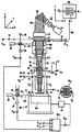
図1は、マスク・パターンを基板上に走査ステップ式に画像形成するような装置の実施例の光学素子を概略的に示す。この装置は、その主コンポーネントとして、投影システムPLを組み込んだ投影カラムを備える。このシステムの上には、画像形成すべきマスク・パターンCを設けたマスクMAのマスク・ホルダMHを配置する。マスク・ホルダはマスク・ステージMTの部分である。基板ステージWTを投影レンズ・システムPLの下に配置する。このテーブルは、感光性を設けた基板Wの基板ホルダWHを備える。マスク・パターンCは、感光層に何回も画像形成しなければならず、回ごとに領域、つまりIC領域Wdが異なる。基板テーブルは、XおよびY方向に移動可能であり、したがって第1IC領域でマスク・パターンを画像形成した後、その後のIC領域をマスク・パターンの下に配置することができる。 FIG. 1 schematically illustrates the optical elements of an embodiment of the apparatus for scanning stepwise imaging of a mask pattern on a substrate. It comprises as its main component a projection column incorporating a projection system PL. On this system, a mask holder MH of a mask MA provided with a mask pattern C to be image-formed is arranged. The mask holder is a part of the mask stage MT. The substrate stage WT is arranged below the projection lens system PL. This table includes a substrate holder WH for a substrate W provided with photosensitivity. The mask pattern C has to be imaged many times on the photosensitive layer, and the area, that is, the IC area Wd is different each time. The substrate table is movable in the X and Y directions, so that after the mask pattern has been imaged in the first IC area, subsequent IC areas can be placed below the mask pattern.
装置は、さらに、例えばクリプトン・フッ素エキシマ・レーザまたは水銀灯などの放射線源LA、レンズ・システムLS、ミラーREおよび集光レンズCOを設けた照明システムを備える。照明システムによって供給された投影ビームPBがマスク・パターンCを照明する。このパターンは、基板WのIC領域上の投影レンズ・システムPLによって画像形成される。投影レンズ・システムは、例えば倍率M=1/4、開口数NA=0.6、および直径22mmの回折で制限された画面サイズを有する。 The apparatus further comprises an illumination system provided with a radiation source LA, for example a krypton fluorine excimer laser or a mercury lamp, a lens system LS, a mirror RE and a condenser lens CO. The projection beam PB provided by the illumination system illuminates the mask pattern C. This pattern is imaged by the projection lens system PL on the IC area of the substrate W. The projection lens system has, for example, a magnification M = 1 /, a numerical aperture NA = 0.6, and a diffraction-limited screen size of 22 mm in diameter.
装置には、さらに幾つかの測定システム、つまりXY面でマスクMAおよび基板Wを相互に対して位置合わせするシステム、基板ホルダの、したがって基板の位置および方位を決定する干渉計システム、および投影レンズ・システムPLの焦点面または画像面と基板Wの表面との間の差を決定する焦点誤差検出システムを設ける。これらの測定システムは、電子信号処理および制御回路およびドライバ、つまり測定システムによって供給された信号に対して、基板および焦点の位置および方位を補正できるアクチュエータを備えるサーボ・システムの部分である。 The apparatus further comprises several measurement systems, namely a system for aligning the mask MA and the substrate W with respect to one another in the XY plane, an interferometer system for determining the position and orientation of the substrate holder and thus of the substrate, and a projection lens. Providing a focus error detection system that determines the difference between the focal plane or image plane of the system PL and the surface of the substrate W; These measurement systems are part of a servo system that includes electronic signal processing and control circuits and drivers, ie, actuators that can correct the position and orientation of the substrate and focus with respect to the signals provided by the measurement system.
位置決めシステムは、図1の右上部分に示すマスクMAの2つの位置決めマークM1およびM2を使用する。図2で示すように、これらのマークは回折格子でよいが、代替的に周囲から光学的に識別される正方形または星形などの他のマークでよい。位置決めマークは2次元でよい。つまり図1のXおよびY方向である2つの相互に直角の方向に延在するか、またはXおよびY方向の両方に延在する他のマークと組み合わせて使用してもよい。基板W、例えば半導体基板は、少なくとも2つの位置決めマークを有し、これは2次元回折格子でよく、そのうち2つP1およびP2を図1に示す。マークP1およびP2は、基板WのIC領域の外側に位置する。格子マークP1およびP2は、位相格子として実現することが好ましく、格子マークM1およびM2は、増幅格子として実現することが好ましい。隣接する回路間のスクライブ線に沿って、他のタイプの位置決めマークを設けてもよい。 The positioning system uses two positioning marks M 1 and M 2 of the mask MA shown in the upper right part of FIG. As shown in FIG. 2, these marks may be diffraction gratings, but may alternatively be other marks, such as squares or stars, which are optically distinguished from the surroundings. The positioning mark may be two-dimensional. That is, it may be used in two mutually perpendicular directions, the X and Y directions of FIG. 1, or in combination with other marks extending in both the X and Y directions. The substrate W, for example a semiconductor substrate, has at least two positioning marks, which may be two-dimensional diffraction gratings, two of which are P 1 and P 2 are shown in FIG. The marks P 1 and P 2 are located outside the IC area of the substrate W. The grating marks P 1 and P 2 are preferably realized as phase gratings, and the grating marks M 1 and M 2 are preferably realized as amplification gratings. Other types of positioning marks may be provided along scribe lines between adjacent circuits.
図1は、オンアクシス・アライメント・ユニットの特殊な実施例、つまりそれぞれ基板の位置決めマークP2をマスクの位置決めマークM2上に位置合わせし、基板の位置決めマークP1をマスクの位置決めマークM1に位置合わせするのに、2本のアライメント・ビームbおよびb’を使用する二重アライメント・ユニットを示す。ビームbは、ミラーなどの反射エレメント30で反射してプリズム26の反射表面27に向かう。表面27はビームbを基板の位置決めマークP2へと反射し、これは放射線の一部をビームb2として関連するマスク・マークMへと送り、ここにマークP2の像が形成される。マークM2の上には、マークM2が渡した放射線を放射線感受性検出器13へと配向するプリズムなどの反射エレメント11が配置される。
FIG. 1 shows a special embodiment of the on-axis alignment unit, that is, the positioning mark P 2 of the substrate is aligned with the positioning mark M 2 of the mask, and the positioning mark P 1 of the substrate is aligned with the positioning mark M 1 of the mask. Figure 2 shows a dual alignment unit that uses two alignment beams b and b 'to align to. The beam b is reflected by a reflecting
第2アライメント・ビームb’は、ミラー31で反射して、投影レンズ・システムPLの反射器29に向かう。この反射器は、ビームb’をプリズム26の第2反射表面28に送り、この表面がビームb’を基板の位置決めマークP1へと配向する。このマークは、ビームb’の放射線の一部をビームb’1としてマスクの位置決めマークM1へと反射し、ここにマークP1の像が形成される。マークM1を通過するビームb’1の放射線は、反射器11’によって放射線感受性検出器13’へと配向される。
The second alignment beam b 'is reflected by the mirror 31 and goes to the reflector 29 of the projection lens system PL. The reflector, the beam b 'to feed on the second reflecting
図2は、2つの等しい基板マークのうち一方を、位相格子の形態で拡大して示す。このような格子は、4つの部分格子P1,a、P1,b、P1,cおよびP1,dで構成することができ、そのうち2つP1,bおよびP1,dがX方向のアライメントに貢献し、他の2つP1,aおよびP1,cがY方向のアライメントに貢献する。2つの部分格子P1,bおよびP1,cは、例えば16μmなどの格子周期を有し、部分格子P1,aおよびP1,dは例えば17.6μmなどの格子周期を有する。各部分格子は、例えば200×200μmなどの寸法を有してよい。原則的に0.1μmより小さいアライメントの正確さは、この格子マークおよび適切な光学系で達成することができる。異なる格子周期を選択することで、アライメント・ユニットの捕捉範囲を拡大することができる。この範囲は、例えば40μmである。 FIG. 2 shows one of the two identical substrate marks in an enlarged manner in the form of a phase grating. Such a lattice can be composed of four sub-lattices P 1, a , P 1, b , P 1, c and P 1, d , of which two P 1, b and P 1, d are X The other two, P 1, a and P 1, c , contribute to the alignment in the Y direction. The two sub-lattices P 1, b and P 1, c have a grating period of, for example, 16 μm, and the sub-lattices P 1, a and P 1, d have a grating period of, for example, 17.6 μm. Each sub-grating may have dimensions such as, for example, 200 × 200 μm. In principle, an alignment accuracy of less than 0.1 μm can be achieved with this grating mark and suitable optics. By choosing different grating periods, the range of capture of the alignment unit can be increased. This range is, for example, 40 μm.
図3は、わずかに変形したアライメント・ユニットの光学素子を、さらに詳細に示す。二重アライメント・ユニットは、2つの別個で等しい位置決めシステムAS1およびAS2を備え、これは投影レンズ・システムPLの光学軸AA’に対して対称に配置される。位置決めシステムAS1はマスク・位置決めマークM2を伴い、位置決めシステムAS2はマスク・位置決めマークM1を伴う。2つの位置決めシステムの対応する要素は、同じ参照番号で示され、システムAS2のそれは、システムAS1のそれと区別するようダッシュを付ける。 FIG. 3 shows the optical elements of the slightly modified alignment unit in more detail. Double alignment unit comprises two separate equal positioning system AS 1 and AS 2, which is arranged symmetrically to the optical axis AA 'of the projection lens system PL. Positioning system AS 1 is associated with a mask alignment mark M 2, positioning system AS 2 is associated with mask positioning marks M 1. Corresponding elements of the two positioning systems are shown with the same reference numbers, the system AS 2 which impart a dash to distinguish them from those of the system AS 1.
次にシステムAS1の構造、さらにマスク・マークM2と例えば基板マークP2との相互位置をこのシステムで決定する方法について説明する。 Then the structure of the system AS 1, further mutual position of the mask mark M 2 for example the substrate mark P 2 describes a method of determining in this system.
位置決めシステムAS1は、放射線源1、例えばアライメント・ビームbを放射するヘリウム・ネオン・レーザを備える。このビームはビーム・スプリッタ2によって基板Wへと反射する。ビーム・スプリッタは、半透明ミラーまたは半透明プリズムで構成してよいが、λ/4プレート3の前にある偏光感受性分割プリズム2で構成することが好ましく、ここでλはビームbの波長である。投影レンズ・システムPLは、基板W上の約1mmの直径を有する小さい放射線スポットBにビームbを集束する。この基板はビームの一部をビームb1としてマスクMAに反射する。ビームb1は投影レンズ・システムPLを横断し、このシステムは放射線スポットVをマスクに画像形成する。基板を投影装置内に配置する前に、放射線スポットVが基板のマークP2上に位置するよう、装置に結合されたアライメント前ステーション、例えば欧州特許出願第0164165号に記載されたステーション内で事前にアライメントする。次に、このマークをビームb1でマスク・マークM2に画像形成する。投影レンズ・システムの倍率Mを考慮に入れて、2つのマークを相互に正確に配置すると、マークP2の像がマークM2に正確に一致するよう、マスク・マークM2の寸法を基板マークP2の寸法に適応させる。
The positioning system AS 1 comprises a
基板Wとの間の経路で、ビームbおよびb1はλ/4プレート4を2回横断し、その光学軸は、光源1から来る直線偏光ビームbの偏光方向に対して45°の角度にある。これで、λ/4を通過したビームb1は、ビームbに対して90°回転した偏光方向を有し、したがってビームb1は偏光分割プリズムを通過する。偏光分割プリズムをλ/4プレートと組み合わせて使用すると、アライメント・ビームを位置決めシステムの放射線経路に結合する場合に、放射線損が最小になるという利点が与えられる。
In the path between the substrate W, the beams b and b 1 traverse the λ / 4
位置決めマークM2を通過するビームb1は、プリズム11で反射し、例えばさらなる反射プリズム12によって放射線感受性検出器13へと配向される。この検出器は、例えば、図2に示す部分格子の数と一致する4つの独立した放射線感受性領域などを有する複合フォトダイオードである。検出器領域の出力信号は、マークM2と基板マークP2の像との一致の尺度である。これらの信号は電気的に処理し、マークPの像がマークMと一致するよう、駆動システム(図示せず)によってマスクと基板とを相互に移動させるために使用することができる。このように、自動位置決めシステムが獲得される。
The beam b 1 passing through the positioning mark M 2 is reflected by the
例えばビームb1の一部分をビームb2として分割する部分的に透明なプリズムなどの形態のビーム・スプリッタ14を、プリズム11と検出器13の間に配置することができる。分割されたビームは、例えば2枚のレンズ15および16などを介して、投影装置のオペレータに位置決めマークP2およびM2が見えるモニタ(図示せず)に結合されたテレビ・カメラ17へと入射する。これで、このオペレータは、2つのマークが一致するか確認し、マークが一致するようマニピュレータによって基板Wを移動させることができる。
A beam splitter 14 in the form of, for example, a partially transparent prism that splits a portion of beam b 1 into beam b 2 can be located between
マークM2とP2に関して以上で説明したのと同様に、マークM1とP2およびマークM1とP1は、相互に対して位置合わせすることができる。最後に述べた2つの位置合わせに、位置決めシステムAS2を使用する。 In a manner similar to that described above with respect to the mark M 2 and P 2, marks M 1 and P 2 and the mark M 1 and P 1 may be aligned with respect to each other. Finally the two alignment mentioned, using the positioning system AS 2.
二重アライメント・ユニットの構造およびアライメント手順に関するさらなる詳細は、米国特許第4778275号を参照し、これは参照により本明細書に組み込まれる。 For further details regarding the structure and alignment procedure of the dual alignment unit, see US Pat. No. 4,778,275, which is incorporated herein by reference.
図1に示すオンアクシス・アライメント・ユニットの実施例は、例えば248nmなどの短い波長を有する投影ビームPB、および例えば633nmなどの非常に長い波長を有するアライメント・ビームを使用する装置には、特に適している。 The embodiment of the on-axis alignment unit shown in FIG. 1 is particularly suitable for devices using a projection beam PB having a short wavelength, for example 248 nm, and an alignment beam having a very long wavelength, for example 633 nm. ing.
投影レンズ・システムは、投影ビームPBの波長に合わせて設計されているので、このシステムPLを、アライメント・ビームによって位置決めマークP1、P2およびM1およびM2を相互に画像形成するために使用すると、差が生じる。例えば、基板位置決めマークは、マスク・位置決めマークが位置するマスク・パターンの面にはなく、そこから所定距離に画像形成され、この距離は、投影ビームとアライメント・ビームの波長の差、および2つの波長の投影レンズ・エレメントの材料の屈折率の差によって決定される。投影ビームが、例えば248nmの波長を有し、アライメント・ビームが633nmの波長を有する場合、この距離は2mmでよい。さらに、前記波長差のため、基板位置決めマークは、所望の倍率とは異なり、しかも波長の差とともに増大する倍率で、マスク・位置決めマークに画像形成される。 Since the projection lens system is designed for the wavelength of the projection beam PB, this system PL is used to image the positioning marks P 1 , P 2 and M 1 and M 2 with each other by means of the alignment beam. Use makes a difference. For example, the substrate alignment mark is not on the plane of the mask pattern where the mask alignment mark is located, but is imaged a predetermined distance therefrom, this distance being the difference between the wavelength of the projection beam and the alignment beam, and two The wavelength is determined by the difference in the refractive indices of the materials of the projection lens element. If the projection beam has a wavelength of, for example, 248 nm and the alignment beam has a wavelength of 633 nm, this distance may be 2 mm. Further, due to the wavelength difference, the substrate positioning mark is image-formed on the mask / positioning mark at a magnification different from the desired magnification and increasing with the wavelength difference.
前記差を補正するため、投影レンズ・システムPLは、追加のレンズ、つまり補正レンズ25を組み込む。補正レンズは、一方で、アライメント・ビームの異なる回折次数のサブビームで、基板位置決めマークから発し、それによって生成されるサブビームが、補正レンズの面にて、これらのサブビームに別個に影響を及ぼせるほど十分に分離され、他方では、この補正レンズが、投影ビームおよびそれで形成されるマスク・パターン像に些細な影響しか与えないような高さで、投影レンズ内に配置される。補正レンズは、投影レンズ・システムのフーリエ面に配置することが好ましい。図3に示すように、アライメント・ビームbおよびb’の主光線が相互に交差する面に補正レンズ25が位置する場合、このレンズを、両方のアライメント・ビームの補正に使用することができる。
To correct for the difference, the projection lens system PL incorporates an additional lens, the
所望に応じて、回折エレメントなどのウェッジ(くさび)または異なる偏向エレメントを、位置決めマークの近位側でアライメント・ビームの経路に配置することができる。このような偏向エレメント(図3には図示せず)があると、検出器13または13’が受ける選択アライメント・ビーム部分内の意図しない位相差によって生じるアライメント誤差を防止することができ、この位相差は、基板の位置決めマークから来るアライメント・ビーム部分の対称軸がマスク・プレートに直角でない場合に生じ、したがってこのプレート内に疑似反射が生じることがある。このような偏向エレメントを設けたアライメント・ユニットが、欧州特許出願第0467445号に記載されている。
If desired, a wedge, such as a diffractive element, or a different deflecting element can be placed in the path of the alignment beam proximal to the registration mark. The presence of such a deflecting element (not shown in FIG. 3) can prevent alignment errors caused by unintended phase differences in the selected alignment beam portion received by
グローバル・アライメントと呼ばれるマスクに対する基板全体の位置合わせに使用し、図1に図示されたグローバル・位置決めマークP1およびP2に加えて、基板には、各IC領域をマスク・パターンに対して別個に位置合わせするよう、IC領域ごとにさらなる位置決めマークを設けてもよい。マークは、例えばZ軸を中心とするマスクの回転を補正できるよう、このような回転を測定するため、さらなる位置決めマークを使用できる3つ以上の位置決めマークも備えることができる。 Was used for alignment of the entire substrate relative to the mask, referred to as global alignment, in addition to the global alignment marks P 1 and P 2 are shown in Figure 1, the substrate, separate each IC area on the mask pattern A further positioning mark may be provided for each IC area so as to perform positioning. The marks may also comprise three or more positioning marks that can use additional positioning marks to measure such rotation, for example, so as to correct the rotation of the mask about the Z axis.
投影装置は、さらに、投影レンズ・システムPLの焦点面と基板Wの表面との偏差を決定する焦点誤差検出システムも備え、したがってこの偏差は、例えばその軸線、つまりZ軸に沿って投影レンズ・システムを移動させることにより、補正することができる。このシステムは、投影レンズ・システムに固定接続されたホルダ(図示せず)内に配置されたエレメント40、41、42、43、44、45および46によって構成することができる。参照番号40は、集束ビームb2を発する放射線源、例えばダイオード・レーザを指す。このビームは、反射プリズム42によって基板上に小さい角度で配向される。基板で反射したビームは、プリズム43によって逆反射器44に配向される。エレメント44は自身内にビームを反射し、したがってビーム(b3’)は再びプリズム43、基板Wおよびプリズム42での反射を介して同じ経路を移動する。
The projection device further comprises a focus error detection system which determines the deviation between the focal plane of the projection lens system PL and the surface of the substrate W, so that this deviation is, for example, along its axis, ie the Z axis. The correction can be made by moving the system. This system can be constituted by
ビームb3’は、部分的に反射するエレメント41および反射エレメント45を介して放射線感受性検出システム46に到達する。この検出システムは、例えば位置依存検出器、または2つの独立した検出器で構成される。このシステム上にビームb3’によって形成される放射線スポットの位置は、投影レンズ・システムの焦点面が基板Wの面と一致する程度によって決定される。焦点誤差検出システムの包括的な説明については、米国特許第4356392号を参照されたい。 Beam b 3 ′ reaches radiation sensitive detection system 46 via partially reflecting element 41 and reflecting element 45. This detection system comprises, for example, a position-dependent detector or two independent detectors. The position of the radiation spot formed by the beam b 3 ′ on this system is determined by the degree to which the focal plane of the projection lens system coincides with the plane of the substrate W. See US Pat. No. 4,356,392 for a comprehensive description of a focus error detection system.
基板ホルダのXおよびY位置を正確に決定するため、ステップ式投影装置に、多軸干渉計システムを設ける。米国特許第4251160号は、2本の測定軸があるシステムについて記載し、米国特許第4737283号は、3本の測定軸があるシステムについて記載している。図1では、このような干渉計システムが、エレメント50、51、52および53によって線図で図示され、測定軸は1本のみ、つまりX軸が図示されている。レーザの形態で放射線源50が発するビームb4は、ビーム・スプリッタ51によって分割されて測定ビームb4,mおよび基準ビームb4,rになる。測定ビームは基板ホルダWHの反射側面54に到達し、反射した測定ビームはビーム・スプリッタ51によって、コーナー・キューブなどの静止逆反射器が反射した基準ビームと組み合わされる。組み合わされたビームの強度は、検出器53で測定され、基板ホルダWHの変位、この場合はX方向の変位は、この検出器の出力信号から導出することができ、このホルダの瞬間位置も決定することができる。
In order to accurately determine the X and Y positions of the substrate holder, the stepper is provided with a multi-axis interferometer system. U.S. Pat. No. 4,251,160 describes a system with two measurement axes, and U.S. Pat. No. 4,737,283 describes a system with three measurement axes. In FIG. 1, such an interferometer system is illustrated diagrammatically by
図1の線図で示すように、単純にするため1つの信号S53で表された干渉計信号、および二重アライメント・ユニットの信号S13およびS’13を、マイクロコンピュータなどの信号処理ユニットSPUに与え、これは前記信号を処理して、アクチュエータACのための信号SACを制御し、これによって基板ホルダをXY面で基板テーブルWTを介して移動させる。 As shown diagrammatically in FIG. 1, the interferometer signals represented by one signal S 53 for simplicity, and the signals S 13 and S '13 of the double alignment unit, a signal processing unit such as a microcomputer given the SPU, which processes the said signals to control signals SA C for actuator AC, thereby moving through the substrate table WT the substrate holder in the XY plane.
図1に示すX測定軸ばかりでなくY測定軸、場合によっては第3測定軸も有する干渉計システムがあると、マスクおよび基板の相互に対する初期アライメント、つまりグローバル・アライメント中に、位置決めマークP1、P2およびM1、M2の位置、およびその間の相互距離を、静止干渉計システムによって画定された座標系内で固定することができる。この干渉計システムは、基板テーブルを非常に正確に移動するためにも使用され、これは第1IC領域から第2IC領域へと非常に正確にステップできるよう、ステップ式投影装置にとって必要である。 With the interferometer system having not only the X measurement axis but also the Y measurement axis, and possibly a third measurement axis as shown in FIG. 1, during the initial alignment of the mask and the substrate with respect to each other, ie global alignment, the positioning mark P 1 , P 2 and M 1 , M 2 , and the mutual distance therebetween can be fixed in the coordinate system defined by the stationary interferometer system. This interferometer system is also used to move the substrate table very accurately, which is necessary for a stepped projection device so that it can very accurately step from the first IC area to the second IC area.
図1に示すように、投影装置が、IC領域内でマスク・パターンを投影する間にマスクと基板とを同時に移動しなければならない走査ステップ式装置である場合、マスクも一方向、つまり走査方向に移動しなければならない。投影レンズ・システムの倍率Mを考慮に入れると、この移動は、基板の対応する移動と同期しなければならない。次に、マスクおよび基板は、投影中は相互に対して静止し、両方とも投影レンズ・システムおよび投影ビームに対しては移動しなければならない。マスクの移動を測定するため、装置には第2干渉計システムを設ける。この干渉計システムは、エレメント50、51、52、53および54と同様の機能を有するエレメント60、61、62、63および64を備える。単純にするため図1では信号S63で表されたマスク干渉研システムからの信号を、信号処理ユニットSPUに与え、ここでこの信号を基板干渉計システムからの対応する信号と比較する。これで、マスクおよび基板が相互に正確な位置を有したり、同期して移動したりしているか確認することができる。
As shown in FIG. 1, when the projection apparatus is a scanning step-type apparatus in which the mask and the substrate must be moved simultaneously while projecting the mask pattern in the IC area, the mask is also moved in one direction, that is, in the scanning direction. Have to go to. This movement must be synchronized with the corresponding movement of the substrate, taking into account the magnification M of the projection lens system. Next, the mask and substrate must be stationary with respect to each other during projection, and both must move with respect to the projection lens system and the projection beam. To measure the movement of the mask, the apparatus is provided with a second interferometer system. This interferometer system includes
マスクのXおよびY方向の位置をXr、Yrで、基板のそれをXw、Ywで、Z軸を中心とする回転をφr,rおよびφz,wで表すと、マスクおよび基板が相互に対して正確に配置された場合、以下の状態を満足する。 Position X r X and Y direction of the mask, with Y r, its substrate in X w, Y w, a rotation about the Z axis phi r, r and phi z, expressed in w, masks and If the substrates are correctly positioned with respect to each other, the following conditions are satisfied.
![]()
![]()
![]()
![]()
![]()
![]()
ここでMは投影レンズ・システムの倍率である。マスクおよび基板が反対方向に移動すると仮定している。これらのエレメントが同じ方向に移動する場合は、上記の状態でMの前にあるマイナス記号をプラス記号で置換しなければならない。 Where M is the magnification of the projection lens system. It is assumed that the mask and the substrate move in opposite directions. If these elements move in the same direction, the minus sign before M in the above situation must be replaced with a plus sign.
これらの条件を満たしたか確認するには、基板の干渉計システムとマスクの干渉計システムとの両方が3つの測定軸を有することで十分である。 To confirm that these conditions have been met, it is sufficient for both the substrate interferometer system and the mask interferometer system to have three measurement axes.
しかし、基板干渉計システムは、5つの測定軸を有することが好ましい。次に、Xw、Ywおよびφz,wばかりでなく、φx,wおよびφy,,w、つまりX軸およびY軸を中心とした傾斜も計算することができる。 However, the substrate interferometer system preferably has five measurement axes. Next, not only X w , Y w and φ z, w , but also φ x, w and φ y ,, w , that is, the tilt about the X axis and the Y axis, can be calculated.
このようなマスクの傾斜を測定できるようにするには、5軸マスク干渉計システムを使用するか、Xr、Yrおよびφz,rを求める3軸干渉計システムと、φx,rおよびφy,r測定用容量センサなどの他のセンサとの組合せを使用することができる。 To be able to measure the tilt of such a mask, a 5-axis mask interferometer system is used, or a 3-axis interferometer system for determining X r , Y r and φ z, r , and φ x, r and Combinations with other sensors such as φ y, r measuring capacitive sensors can be used.
Xw、Yw、φx,w'およびφy,,wおよびXr、Yr、φz,r、φx,r、φy,rを、焦点誤差検出システムZwおよびZr、つまり基板およびマスクのZ軸に沿った位置の助けを借りて測定することができれば、条件(1)、(2)および(3)ばかりでなく、以下の条件も満たすか確認することができる。 X w , Y w , φ x, w ′ and φ y ,, w and X r , Y r , φ z, r , φ x, r , φ y, r are referred to as focus error detection systems Z w and Z r , That is, if the measurement can be performed with the help of the positions of the substrate and the mask along the Z axis, it is possible to confirm whether not only the conditions (1), (2) and (3) but also the following conditions are satisfied.
![]()
![]()
![]()
![]()
![]()
![]()
マスクの位置決めマークと基板の位置決めマークを相互に対して相互位置合わせする図3に関して説明したオンアクシス・アライメント・ユニットは、所与の最小値までの線幅を有する像を形成するステップ式投影装置と走査ステップ式投影装置との両方に非常に適していることが判明した。しかし、IC製造に新規技術を使用し、像の線幅が縮小すると、既知のアライメント・ユニットの正確さおよび信頼性に関する限り、問題が生じる。線幅を縮小した場合、アライメントの正確さを向上させなければならない。前記CMPプロセスを使用すると、基板格子マークに非対称性が持ち込まれ、したがって1次サブビームを使用するアライメント手順が信頼できなくなる。さらに、1つの波長を有するアライメント・ビームを使用する場合、位置決めマークの格子溝の深さに厳密な要件を設けなければならず、その要件を満たすには、困難さが増してしまう。 The on-axis alignment unit described with reference to FIG. 3 for aligning the registration mark of the mask and the registration mark of the substrate with respect to each other is a step-type projection apparatus for forming an image having a line width up to a given minimum value. And a scanning step projector. However, the use of new technologies in IC manufacturing and the reduction in image linewidth present problems as far as the accuracy and reliability of known alignment units are concerned. When the line width is reduced, the accuracy of the alignment must be improved. The use of the CMP process introduces asymmetry into the substrate grid marks, thus making the alignment procedure using the primary sub-beam unreliable. Furthermore, when an alignment beam having one wavelength is used, a strict requirement must be set for the depth of the grating groove of the positioning mark, and it becomes more difficult to meet the requirement.
これらの問題は全て、基板マークの位置合わせにオフアクシス・アライメント・ユニットを使用し、より高次のサブビーム、つまり位置合わせに2以上の回折次数を有するサブビームを使用することにより解決することができる。基板マークのアライメントの実行にもはや投影レンズ・システムが関与しないので、さらにサブビームを、特により高次のサブビームを使用する自由度が高くなる。アライメント・ユニットの解像力はサブビームの次数の増加とともに向上するので、アライメントの正確さを大幅に向上させることができる。特に、より高次のサブビームは基板の格子マークの縁によって決定され、格子の中心と比較して、これらの縁は格子の対称に影響する前記CMPプロセスおよび他の措置からの影響が少ないので、格子マークの非対象に関する問題が、ほとんど解消される。さらに、格子溝の深さに課された要件が大幅に緩和できるよう、複数の波長を有するアライメント放射線を使用することも可能である。 All of these problems can be solved by using an off-axis alignment unit for substrate mark alignment and using higher order sub-beams, ie, sub-beams with diffraction orders of 2 or more, for alignment. . Since the projection lens system is no longer involved in performing the alignment of the substrate marks, there is more freedom to use further sub-beams, especially higher order sub-beams. Since the resolution of the alignment unit increases with the order of the sub-beams, the accuracy of the alignment can be greatly improved. In particular, the higher order sub-beams are determined by the edges of the grid marks on the substrate, and since these edges are less affected by the CMP process and other measures that affect the symmetry of the grating as compared to the center of the grating, The problem of lattice mark asymmetricity is almost eliminated. In addition, it is possible to use alignment radiation with multiple wavelengths so that the requirements imposed on the depth of the grating grooves can be greatly reduced.
以下で解明されるように、回折次数は、電子的手段および/または関連するソフトウェアによってではなく、本発明によるアライメント・ユニットの光学素子によって、相互から分離される。その結果、信号の振幅を測定する必要はないが、この種の技術ではより伝統的な位相測定を使用することができる。 As will be elucidated below, the diffraction orders are separated from each other by the optical elements of the alignment unit according to the invention, rather than by electronic means and / or associated software. As a result, it is not necessary to measure the amplitude of the signal, but more traditional phase measurements can be used with this type of technique.
図4は、オフアクシス・位置決めシステムを有するリソグラフィ・システムの略図である。オフアクシス・位置決めシステムは、2つの異なる波長で位置決めマークを照明する2つの放射線源70、例えば赤いレーザおよび緑のレーザを有する。両方のレーザは、位置決めマークを同時に照明し、反射光は別個の検出器チャネル(例えば赤いチャネルおよび緑のチャネル)に配向される。したがって、2つの波長チャネルそれぞれの信号が並列で獲得される。また、2つの波長それぞれで、幾つかの回折次数を別個に検出することができ、したがって信号を並列に出力する複数の色/次数チャネルが提供される。位置決定ユニットPDUは、検出システムの複数の色/次数チャネルと連絡する。位置決定ユニットPDUは、特定の機能を実行する固定配線専用装置であるか、所望の機能を実行するようプログラムされたプログラム可能なコンピュータを含むことができる。また、図1に示したSPUとは別個のユニットか、ソフトウェアを通してSPUに実装することができる。位置決定ユニットDPUは、色/次数チャネルのうち少なくとも2つからの信号を処理し、検出中の位置決めマークの位置を決定する。
FIG. 4 is a schematic diagram of a lithography system having an off-axis positioning system. The off-axis positioning system has two
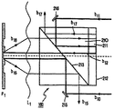
図5は、本発明の実施例によるオフアクシス・アライメント・ユニットの略図である。本明細書で説明する位置決めシステムの多くの構造的特徴は、米国特許第6297876号に記載されたものと同様、または同じであり、その全内容は参照により本明細書に組み込まれる。格子の形態の基板マークを、P1で示す。この格子に入射する波長λを有する平行アライメント・ビームbは、格子に直角に異なる角度αn(図示せず)で延在する幾つかのサブビームに分割され、その角度は既知の格子数式で定義される。 FIG. 5 is a schematic diagram of an off-axis alignment unit according to an embodiment of the present invention. Many structural features of the positioning system described herein are similar or identical to those described in US Pat. No. 6,297,876, the entire contents of which are incorporated herein by reference. The substrate marks in the form of a grid, indicated by P 1. The parallel alignment beam b with wavelength λ incident on this grating is split into several sub-beams extending at different angles α n (not shown) perpendicular to the grating, the angle being defined by a known grating formula. Is done.

ここでNは、回折次数、Pは格子周期である。 Here, N is the diffraction order, and P is the grating period.
格子で反射したサブビームの経路は、レンズ・システムL1を組み込み、これはサブビームの様々な方向を、そのサブビームの面73における様々な位置unに変換する。
Path of the sub-beams reflected by the grating incorporates a lens system L 1, which is a different direction of sub-beams is converted into various positions u n in the
![]()
![]()
この面に、様々なサブビームをさらに分離する手段を設ける。そのため、この面にプレートを配置することができ、それに例えばウェッジの形態の偏向エレメントを設ける。図5では、ウェッジ・プレートをWEPで示す。ウェッジを、例えばプレートの後側に設ける。次に、プリズム72をプレートの前側に設けることができ、これによりHe−Neレーザなどの放射線源70から来るアライメント・ビームを、アライメント・ユニットに結合することができる。このプリズムは、0次サブビームが検出器に到達するのを防止することもできる。ウェッジの数は、使用するサブビームの数に対応する。図示の実施例では、プラスの次数の次元ごとに6個のウェッジがあり、したがってサブビームは、アライメントのために7次まで使用することができる。全てのウェッジは異なるウェッジ角度を有し、したがって異なるサブブームの最適な分離が獲得される。
This surface is provided with means for further separating the various sub-beams. For this purpose, a plate can be arranged on this surface, which is provided with a deflecting element, for example in the form of a wedge. In FIG. 5, the wedge plate is indicated by WEP. A wedge is provided, for example, on the rear side of the plate. Next, a
第2レンズ・システムL2を、ウェッジ・プレートの背後に配置する。このレンズ・システムは、マークP1を基準プレートRGPの面に画像形成する。ウェッジ・プレートがないと、全てのサブビームが基準面に重ねられてしまう。ウェッジ・プレートを通る様々なサブビームが異なる角度で偏向するので、サブビームが形成した像は、基準面の様々な位置に到達する。この位置Xnは下式によって与えられる。 A second lens system L 2, is arranged behind the wedge plate. The lens system imaging the mark P 1 on the surface of the reference plate RGP. Without the wedge plate, all sub-beams would be superimposed on the reference plane. As the various sub-beams passing through the wedge plate deflect at different angles, the images formed by the sub-beams reach various positions on the reference plane. This position Xn is given by the following equation.
![]()
![]()
ここでγは、サブビームがウェッジ・プレートによって偏向する角度である。 Where γ is the angle at which the sub-beam is deflected by the wedge plate.
これらの位置に、図6で示すように基準格子G90〜G96を設けることができる。独立した検出器90〜96をこれらの基準格子それぞれの背後に配置する。各検出器の出力信号は、基板格子P1の像が関連する基準格子と一致する程度によって決定される。したがって、基板格子のアライメントの程度、したがって基板のアライメントの程度を、各検出器90〜96で測定することができる。しかし、実行する測定の正確さは、使用するサブビームの次数によって決定される。この次数が大きくなるにつれ、正確さが向上する。図6では、単純にするため、全ての基準格子G90〜G96が同じ格子周期を有すると仮定している。しかし、実際には各格子の格子周期は、関連するサブビームの次数に適応する。次数が大きくなるにつれ、格子周期が小さくなり、検出できるアライメント誤差が小さくなる。 These positions may be provided a reference grating G 90 ~G 96 as shown in Figure 6. Independent detectors 90-96 are located behind each of these reference gratings. The output signal of each detector is determined by the extent to which the image of the substrate grating P 1 coincides with the relevant reference grating. Thus, the degree of alignment of the substrate grid, and thus the degree of alignment of the substrate, can be measured by each detector 90-96. However, the accuracy of the measurements performed is determined by the order of the sub-beams used. As this order increases, the accuracy improves. In Figure 6, for simplicity, all the reference gratings G 90 ~G 96 are assumed to have the same grating period. However, in practice, the grating period of each grating will adapt to the order of the associated sub-beam. As the order increases, the grating period decreases, and the detectable alignment error decreases.
これまでは、1セットの回折次数しか考慮していない。知られているように、回折格子は、+1、+2、+3などの次数のサブビームに加えて、回折次数が−1、−2、−3などのサブビームも形成する。格子像を形成するには、プラス次数とマイナス次数のサブビームの両方を使用することができる。つまり格子マークの第1像は、+1および−1次のサブビームが共同して形成し、第2像は+2および−2次のサブビームが共同して形成し、以下同様である。+1次および−1次のサブビームでは、ウェッジを使用する必要がないが、路長の差を補償する平行平面プレートを、ウェッジ・プレートの面で、これらのサブビームの様々な位置に設けることができる。したがって、2〜7次には、プラスの次数とマイナスの次数の両方で6個のウェッジが必要である。 So far, only one set of diffraction orders has been considered. As is known, diffraction gratings form sub-beams with diffraction orders of -1, -2, -3, etc., in addition to sub-beams of order +1, +2, +3, and so on. Both positive and negative order sub-beams can be used to form a grating image. That is, the first image of the grating mark is formed jointly by the +1 and -1 order sub-beams, the second image is formed jointly by the +2 and -2 order sub-beams, and so on. For the +1 order and -1 order sub-beams, no wedges need to be used, but parallel plane plates that compensate for path length differences can be provided at various positions of these sub-beams in the plane of the wedge plate. . Therefore, for the 2nd to 7th orders, 6 wedges are required in both the positive and negative orders.
図7は、図5の実施例のウェッジの働きをさらに明瞭に示す。より概略的な図7では、第1レンズ・システムL1および第2レンズ・システムL2を波線で示す。明快さを期して、1次のサブビームb(+1)およびb(−1)、7次のサブビームb(+7)およびb(−7)、および別の次数のサブビームb(+i)およびb(−i)、例えば5次を示す。図7で示すように、ウェッジ80および80’のウェッジ角度、つまりウェッジの傾斜面がウェッジ・プレートWEPの表面と形成する角度は、サブビームb(+7)およびb(−7)が平行方向に偏向し、第2レンズ・システムによって1つの基準格子G96上に収束するような角度である。また、サブビームb(+1)およびb(−1)は、関連するウェッジ82および82’によって平行方向に偏向し、1つの基準格子G91上に集束する。1次サブビームは偏向せず、第2レンズ・システムによって1つの基準格子G93上に集束する。各回折次数のプラスの次数とマイナスの次数の両方を使用することにより、基板格子マークP1の真実の像が関連する基準格子上に形成され、使用可能な放射線が最大限に使用される。
FIG. 7 shows more clearly the operation of the wedge of the embodiment of FIG. 7, the first lens system L 1 and the second lens system L 2 are indicated by dashed lines. For clarity, the first-order sub-beams b (+1) and b (-1), the seventh-order sub-beams b (+7) and b (-7), and the other-order sub-beams b (+ i) and b (-) i), for example, the fifth order. As shown in FIG. 7, the wedge angles of the
図8は、マークP1の面、およびレンズ・システムL1およびL2の基準格子プレートに対する好ましい位置、およびこれらのレンズ・システムの焦点距離を示す。レンズ・システムは焦点距離f1を有し、このシステムはマークP1の面から距離f1に配置される。レンズ・システムL1は、サブビームの主光線を光軸OO’に平行な方向に偏向する。第1レンズ・システムと第2レンズ・システム間の距離はf1+f2に等しく、これによりf2は第2レンズ・システムの焦点距離である。基準格子プレートは第2レンズ・システムから距離f2に配置される。2つのレンズ・システム間の経路と同様、サブビームの主光線は光軸OO’に平行であり、ウェッジ・プレートの位置は重要でない。 Figure 8 shows a preferred position relative to the plane of the mark P 1, and a lens system L 1 and the reference grating plate L 2, and the focal length of the lenses system. Lens system has a focal length f 1, the system is arranged from the plane of the mark P 1 on the distance f 1. Lens system L 1 deflects the chief ray of the sub-beams in a direction parallel to the optical axis OO '. The distance between the first lens system and the second lens system is equal to f 1 + f 2 , whereby f 2 is the focal length of the second lens system. Reference grid plate is arranged at a distance f 2 from the second lens system. As with the path between the two lens systems, the chief ray of the sub-beam is parallel to the optical axis OO ', and the position of the wedge plate is not important.
図4の実施例では、同じ回折次元でプラスおよびマイナスの次数のサブビームが、第2レンズ・システムによって関連する基準格子上に正確に重ねられるよう偏向するため、2つの関連するウェッジの相互品質には、より厳密な要件を設定する。この品質要件は、ウェッジの傾斜面およびウェッジ角度の品質の関連する。 In the embodiment of FIG. 4, the sub-beams of the same diffraction dimension plus and minus orders are deflected by the second lens system to be exactly superimposed on the associated reference grating, so that the mutual quality of the two associated wedges is Sets stricter requirements. This quality requirement is related to the quality of the wedge slope and wedge angle.
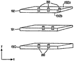
前記要件を軽減し、アライメント・ユニットの公差を緩和するため、図9に示す偏向エレメントの構造を使用することが好ましい。サブビームごとに1つの別個のウェッジにする代わりに、全てのサブビームに共通の幾つかの、例えば3つのウェッジ・プレート190、191、192を使用する。図9はウェッジ・プレートの斜視図を示し、図10は側面図を示す。ウェッジ角度、つまりプレートの上面と下面との間の角度、つまりプレート192の場合は面192aと面192bの間の角度は、3つのプレートで異なる。プレートの1つ、例えばプレート190は、他のプレートの角度とは反対のウェッジ角度を有する。このプレートには、幾つかの開口200を設けるが、図9にはその幾つかしか図示されていない。これらの開口は、サブビームが関連するプレートに入射する位置に配置される。しかし、このような位置全てに開口があるわけではない。サブビームがプレートの開口に入射すると、そのプレートによって偏向されない。
In order to reduce the above requirements and to reduce the tolerance of the alignment unit, it is preferable to use the structure of the deflection element shown in FIG. Instead of one separate wedge for each sub-beam, several, eg three,
サブビームは、プレートに向かう途中で0個、1個または2個の開口に遭遇する。1次サブビームのみが0個の開口に遭遇し、どのプレートでも偏向しない。図10では、サブビームの1本がプレートを通る経路を示す。このサブビームは、第1プレート190によって右に偏向する。その後、このサブビームは左へ前より小さい角度偏向する。最後に、このサブビームはプレオート192の開口200を通過し、したがってさらなる偏向は生じない。サブビームごとに、開口の数およびこのような開口があるプレートの次数は、他のサブビームとは異なり、したがってサブビームは全て、異なる方向に偏向する。3つのプレートの組合せ23=8により、異なる偏向方向を実現できることが明白である。同じ回折次数の1対のサブビームは、同じウェッジ・プレートで偏向するので、これらのサブビームが平行方向に偏向されないという危険は最小になる。
The sub-beam encounters zero, one or two apertures on its way to the plate. Only the primary sub-beam encounters zero apertures and does not deflect any plates. FIG. 10 shows the path through which one of the sub-beams passes through the plate. This sub-beam is deflected to the right by the
図5、図6の実施例では、1から7の次数のサブビームを使用し、したがってX方向でのアライメントには7つの基準格子G90〜G96が必要である。Y方向のアライメントには、図6に示すように、7本のサブビームを7つのさらなる基準格子G93〜G104と一緒に使用することができる。次に、図5の実施例では、第2組のウェッジ12個をY方向でウェッジ・プレートに配置する。図9の実施例では、第1組のウェッジ・プレートの前または後に、第2組の3個のウェッジ・プレートをサブビームの経路に配置し、第2組のプレートはサブビームをY方向に偏向する。基板マークは、図2に示すマーク、または他のタイプのマーク、例えばスクライブ線に沿って設けたマークでよい。1次サブビームでは、4つの格子部分がある同様の基準格子を使用することができ、そのうち2つは16.0μmの格子周期を有し、他の2つの格子部分は、図6に示すように17.6μmの格子周期を有する。他の基準格子は、基板格子P1の16μmという周期を有する格子部分の関連回折次数と対応する1つの格子周期しか有さない。これで、図2の格子マークP1に関連する44μmという捕捉範囲が維持される。
In the embodiment of FIGS. 5 and 6, sub-beams of
図5、図6の実施例では、最高次数を有するサブビームが、最大角度を通る偏向エレメントによって偏向される。しかし、これは必要ではない。ある状況では、例えば格子像の光学収差を最小にするため、この次数を変更してよい。これは、図6に示すように、昇順次数のサブビームがウェッジによってプラスの角度とマイナスの角度で交互に偏向することの理由にもなる。 In the embodiment of FIGS. 5 and 6, the sub-beam with the highest order is deflected by a deflecting element passing through the maximum angle. But this is not necessary. In some situations, this order may be changed, for example, to minimize optical aberrations in the grating image. This is also the reason that the ascending sequential number of sub-beams are alternately deflected by the wedge at positive and negative angles, as shown in FIG.
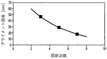
任意の非対称の基板マークP1で十分に正確な状態で位置合わせできるよう、検出すべき最低回折次数は、コンピュータ・シミュレーションで決定することができる。このようなシミュレーションは、例えば1次サブビームを使用する場合に維持される150nmのアライメント誤差などが、5次サブビームを使用すると20nmに低下できることを証明している。 The lowest diffraction order to be detected can be determined by computer simulation so that any asymmetric substrate mark P 1 can be aligned with sufficient accuracy. Such simulations demonstrate that, for example, a 150 nm alignment error maintained when using a primary sub-beam can be reduced to 20 nm using a fifth-order sub-beam.
原則的に、検出できる最高次数は、依然として検出できる最低強度、およびレンズ・システムL1、L2の開口数によって決定される。知られているように、回折格子によって形成されるサブビームの強度は、このサブビームの次数の増加と共に低下し、サブビームの強度は、このサブビームの次数の平方に逆比例する。7次サブビームの場合、強度は1次サブビームの約1/50になる。しかし、オフアクシス・アライメント・ユニットを横断する時にアライメント・ビームが経験する反射によって生じる強度損は、オンアクシス・アライメント・ユニットを横断する場合よりはるかに小さい。最後に言及したユニットでは、アライメント・ビームは、反射損が生じる約100の表面に遭遇し、最初に言及したユニットでは、例えばその表面のうち20にしか遭遇しない。全反射損がオフアクシス・アライメント・ユニットの4の関数の場合、7次アライメント・サブビームは、オンアクシス・アライメント・ユニットの1次アライメント・ビームと同じ強度を有することができる。 In principle, the highest order that can be detected is determined by the lowest intensity that can still be detected and the numerical aperture of the lens systems L 1 , L 2 . As is known, the intensity of the sub-beam formed by the diffraction grating decreases with increasing order of the sub-beam, and the intensity of the sub-beam is inversely proportional to the square of the order of the sub-beam. In the case of the seventh sub-beam, the intensity is about 1/50 of that of the first sub-beam. However, the intensity loss caused by the reflections experienced by the alignment beam when traversing the off-axis alignment unit is much less than when traversing the on-axis alignment unit. In the last-mentioned unit, the alignment beam encounters about 100 surfaces where reflection losses occur, and in the first-mentioned unit, for example, only 20 of its surfaces. If the total reflection loss is a function of four of the off-axis alignment unit, the seventh-order alignment sub-beam can have the same intensity as the primary alignment beam of the on-axis alignment unit.
光学システムL1、L2がNの回折次数を有するサブビームを通過させねばならない開口数NAnは、下式によって与えられる。 The numerical aperture NA n through which the optical system L 1 , L 2 must pass a sub-beam having N diffraction orders is given by:
7次サブビームと、格子周期p=16μmおよび波長λ=544nmを有する基板格子マークでは、所望の開口数は約0.24であり、これは非常に満足できる数である。 For a 7th-order sub-beam and a substrate grating mark having a grating period p = 16 μm and a wavelength λ = 544 nm, the desired numerical aperture is about 0.24, which is a very satisfactory number.
十分に安定したシステムを保証するため、クォーツで構成することが好ましい単一のプレートRGPに、様々な基準格子を設ける。このプレートの寸法、したがって第2レンズ・システムの画面サイズは、基準格子の寸法d1およびその相互距離d2によって決定される。距離および寸法は、例えば両方とも0.2mmであり、したがってプレートRGPのXおよびY方向の寸法dxおよびdy、および所望のフィールド直径は約3mmである。 To ensure a sufficiently stable system, a single plate RGP, preferably made of quartz, is provided with various reference gratings. The dimensions of this plate, and thus the screen size of the second lens system, are determined by the dimensions d 1 of the reference grating and its mutual distance d 2 . The distances and dimensions are, for example, both 0.2 mm, so that the dimensions d x and d y in the X and Y directions of the plate RGP and the desired field diameter are about 3 mm.
図5の実施例の別個のウェッジは、ガラスまたはクォーツで作成し、クォーツ・プレートに固定することができる。この構造は、高度の安定性を示す。ウェッジは透明な合成材料、例えば紫外線硬化性プラスチックで作成してもよい。その場合、特に光学で知られている複製技術を使用し、ウェッジ構造全体を型により1回でこの材料の薄い層に印刷することが好ましく、この層を、例えばクォーツ基板に適用する。既に述べたように、別個のウェッジの代わりに、開口を設けたウェッジ・プレートを使用することが好ましい。別個のウェッジまたはウェッジ・プレートの代わりに、1つの次数しか使用しない回折格子など、他の偏向手段を代替的に使用することができる。さらに、材料のプレートの屈折率変動のパターンによって構成した偏向構造を使用することが可能であり、このパターンは、例えばイオン注入によって設けられる。 The separate wedges of the embodiment of FIG. 5 can be made of glass or quartz and fixed to a quartz plate. This structure exhibits a high degree of stability. The wedge may be made of a transparent synthetic material, for example a UV curable plastic. In that case, it is preferable to print the entire wedge structure in one go on a thin layer of this material by means of a mold, in particular using replication techniques known in optics, which layer is applied, for example, to a quartz substrate. As already mentioned, it is preferred to use a wedge plate with openings instead of a separate wedge. Instead of a separate wedge or wedge plate, other deflection means may alternatively be used, such as a diffraction grating using only one order. Furthermore, it is possible to use a deflection structure constituted by a pattern of refractive index variation of the plate of material, which pattern is provided, for example, by ion implantation.
基板マークの溝深さに対する要件が厳格になりすぎないようにするため、2つの波長、例えば633nmおよび532nmを有するアライメント放射線が適切であることが判明した。式(7)および式(8)から明白なように、アライメント格子がサブビームを偏向する角度、およびこれらのビームがレンズ・システムL1の後部焦点面で占有する位置が波長によって決定されるという事実を利用することができる。原則的に、異なる波長の次数は相互から識別することができる。しかし、さらなる測定をせずに、所与の次数、例えば第1波長(633nm)の2次が、例えば第2波長(532nm)の2次と3次の間に来てもよい。異なる波長の次数を相互からよりよく分離するため、異なる波長のビームが基板格子P1に異なる角度で入射することを保証することができる。2つの回折次数を使用する場合は、図11に示すような状態がレンズ・システムL1の後焦点面に生成される。次に、第1波長の様々な次数には位置110〜137の第1十字形パターンがあり、第2波長の様々な次数の位置138〜165の第2十字形パターンがある。図7の中心にある二重矢印によって示すように、これらのパターンは相互に対してずれ、これは異なる波長のアライメント・ビームの入射角が異なるからである。これらの角度は、集束高価によって生じるアライメント誤差を防止するよう、可能な限り小さく維持しなければならない。2つの波長を使用する場合、偏向エレメントがあるプレートは、言うまでもなく図11に示すような状態に適合しなければならない。つまり、特に24個の別個のウェッジではなく48個のウェッジを使用しなければならないか、6枚のウェッジ形プレートの代わりに、このようなプレートを12枚使用しなければならない。 Alignment radiation having two wavelengths, for example 633 nm and 532 nm, has been found to be suitable, in order not to make the requirements for the groove depth of the substrate mark too stringent. Equation (7) and As is apparent from equation (8), the fact that the angle at which the alignment grating deflects the sub-beams, and the position where the beams are occupied by the back focal plane of the lens system L 1 is determined by the wavelength Can be used. In principle, the orders of the different wavelengths can be distinguished from each other. However, without further measurement, a given order, for example the second order at the first wavelength (633 nm), may for example fall between the second and third order at the second wavelength (532 nm). To better isolate the order of the different wavelengths from each other, it is possible to beams of different wavelengths to ensure that incident at different angles on the substrate grating P 1. When using two diffraction orders, the state shown in FIG. 11 is generated in the focal plane of the lens system L 1. Next, various orders of the first wavelength have a first cross pattern at positions 110-137 and various orders of the second wavelength have a second cross pattern at positions 138-165. As indicated by the double arrows in the center of FIG. 7, these patterns are offset with respect to each other because the angles of incidence of the alignment beams of different wavelengths are different. These angles must be kept as small as possible to prevent alignment errors caused by high focusing costs. When using two wavelengths, the plate with the deflecting element must of course conform to the situation as shown in FIG. That is, in particular, 48 wedges must be used instead of 24 separate wedges, or 12 such plates must be used instead of 6 wedge-shaped plates.
2つの波長でのアライメントに対する代替法が、図12に図示されている。この図では、参照番号160は偏向感受性ビーム・スプリッタを示す。このビーム・スプリッタは、He−Neレーザからの第1波長λ1、例えば633nmを有し、第1偏光方向を有する第1アライメント・ビームbを受け、このビームを基板位置決めマークP1に渡す。このビーム・スプリッタには、第2波長λ2、例えば532nmを有し、周波数2倍器の前にあるYAGレーザから来る第2アライメント・ビームb5も入射する。ビームb5は、ビームbに直角の偏光方向を有し、したがってビームb5は基板マークP1へと反射する。ビームbおよびb5の主光線は、ビーム・スプリッタによって一致させられ、したがってこれらのビームが1本のビームとしてマークP1に渡されることが保証されている。ビームbおよびb5は、マークで反射した後、再びビーム・スプリッタによって分割される。独立したアライメント・ユニット170、180がこれらのビームそれぞれにある。これらのユニットはそれぞれアライメント・ビームを発し、ビーム・スプリッタを介して、基板マークから来る異なる回折次数のサブビームを受ける。これらのユニットそれぞれで、図5に関して説明したように、基板マークの像が異なるサブビームで異なる基準格子上に形成される。そのため、各ユニットには、レンズ・システムL1、L2(L1’、L2’)、ウェッジ・プレートWEP(WEP’)、および図9または一連のウェッジ形プレート、基準格子RGP(RGP’)があるプレート、幾つかの検出器90〜96(90’〜96’)、および結合プリズム72(72’)を介してシステムに結合されたビームを有する放射線源70(70’)を設ける。
An alternative to alignment at two wavelengths is illustrated in FIG. In this figure,
図13は、特殊な種類のビーム・スプリッタ160を使用するアライメント・ユニットの実施例の一部を示す。このビーム・スプリッタは、偏光感受性ビーム分割プリズム210、1/4波長プレート211および反射器212を備える。異なる波長を有し、源(図示せず)から来るビームb10およびb11を太線で示し、格子マークP1が反射するビームを細線で示す。ビームb10およびb11は同じ偏光方向を有する。第1ビームb10は反射器215で反射して、プリズム210内の偏光感受性ビーム分割層213に向かう。この層はビームb10を格子マークP1へと反射する。格子マークで反射し、異なる回折次数のサブビームに分割された放射線は、1本のビーム線b15で表される。ビームb15は層213で反射して、関連の偏光エレメントの構造および検出器(図13には図示せず)に向かう。
FIG. 13 shows a portion of an embodiment of an alignment unit that uses a special type of
第2ビームb11は反射器216で反射してビーム分割層213に向かい、これはビームを1/4波長プレート212へと反射する。ビームb11は、このプレートを通過すると、このプレートの背側で反射層212によって反射し、したがって2回目でプレート211を通過する。プレート211を出たビームb12は、元のビームb11の偏光方向に対して90°回転した偏光方向を有する。ビームb12は、ビーム分割層213を通過して、格子マークP1に到達することができる。このマークで反射する放射線も、1本のビーム線b16で表す。このビームは最初にビーム分割層213を通過し、次に1/4波長プレートを2回横断して、最終的に層213で反射して、ウェッジおよび検出器(図13には図示せず)の関連構造に向かう。明快さを期して、図13には反射ビームb16およびb17は空間的に分離されたビームとして図示されているが、実際には、これらのビームは一致する。マークP1の位置におけるビームb10およびb11についても、同じことが当てはまる。
The second beam b 11 is reflected by
図12、図13の実施例では、第1レンズ・システムL1は、図13に示すようにビーム・スプリッタ216と格子マークP1との間に配置することが好ましい。これは、波長が異なる2本のビームに、このようなレンズ・システムが1つした必要でないという追加の利点を有する。反射したビームには、別個の第2レンズ・システムL2(図13には図示せず)が依然として必要である。
In the embodiment of FIGS. 12 and 13, the first lens system L 1 is preferably arranged between the
上述した様々な実施例では、検出器を基準格子の真後ろに配置する。しかし実際には、基準格子の背後には、1束の撮像ファイバを配置することができ、これは基準格子および基準格子、および基板格子マークの重畳画像をそれぞれ、遠隔位置の検出器に画像形成し、これは、装置全体の設計およびこの装置の性能に関して、さらに都合がよい。例えば、異なる回折次数のサブビームによって形成される画像間のクロストークを減少させ、信号増幅器および電子プロセッサによって発生する熱をアライメント・ユニットおよび装置から遠ざけておくことができる。放射線源も、アライメント・ユニットから遠い位置に配置し、その放射線をファイバの照明束によってユニットに案内することもできる。この方法で、放射線源から発生した熱を、アライメント・ユニットおよび統制装置から遠ざけておくことができる。 In the various embodiments described above, the detector is located directly behind the reference grid. However, in practice, behind the reference grating, a bundle of imaging fibers can be placed, which images the reference grating and the superimposed image of the reference grating and the substrate grating mark, respectively, to a remote detector. However, this is even more convenient with regard to the overall device design and the performance of the device. For example, crosstalk between images formed by sub-beams of different diffraction orders can be reduced, and heat generated by signal amplifiers and electronic processors can be kept away from alignment units and devices. The radiation source may also be located remote from the alignment unit and its radiation guided to the unit by a bundle of fibers. In this way, heat generated from the radiation source can be kept away from the alignment unit and the controller.
ビームb15およびb17の一方について、プリズム216と第2レンズ・システムL2の間に、部分的に透過する反射器を配置し、このビームの一部をカメラへと分割することができ、カメラはミラーと一緒に基板マークの視覚像を装置のオペレータに提供する。
For one of the beams b 15 and b 17 , a partially transmissive reflector can be arranged between the
様々な検出器信号の使用については、様々な可能性がある。1次サブビームによって、そのサブビームに関連する検出器の信号を処理することにより、アライメントから開始してよい。その後、2次サブビームに関連する検出器の信号を、さらに細かい位置合わせに使用し、次に3次サブビームに関連する検出器の信号を、さらに細かい位置合わせに使用し、以下同様とすることができる。使用するサブビームが依然として確実な方法で検出されるほど十分な強度を有する限り、これを続行することができる。 There are different possibilities for the use of different detector signals. The alignment may start with the primary sub-beam processing the detector signal associated with that sub-beam. Thereafter, the detector signal associated with the secondary sub-beam may be used for finer alignment, then the detector signal associated with the tertiary sub-beam may be used for finer alignment, and so on. it can. This can be continued as long as the sub-beams used still have sufficient intensity to be detected in a reliable manner.
別の可能性は、特定の回折次数の強度は、基板に所与のプロセス層を設けた場合、他の回折次数を代償として増加する、という認識に基づく。その倍、位置合わせについて、好ましい次数を直接選択することができる。ある状況では、前記可能性を組み合わせてもよい。 Another possibility is based on the recognition that the intensity of a particular diffraction order increases at the cost of another diffraction order when a substrate is provided with a given process layer. Again, the preferred order can be directly selected for alignment. In some situations, the possibilities may be combined.
基板のバッチをマスク・パターンで照明する前、または生産日の開始時に、アライメント・ユニットを校正することも可能である。幾つかの基板マークの位置について、各回折次数について検出器信号を測定する。その測定の結果を、基板マークの各位置について各回折次数の検出器信号の値を表示するグラフまたは表に記憶する。基板の照明中に、比較的低い回折次数、例えば最初の3つの次数について比較的大きい検出器信号のみを測定することにより、アライメント測定を実行することができる。内挿によってより高い回折次数、例えば7次について、対応する値を決定することができる。この方法にて、高い解像度および大きい信号振幅でアライメント誤差を決定することが可能である。 It is also possible to calibrate the alignment unit before illuminating the batch of substrates with the mask pattern or at the beginning of the production day. For several substrate mark locations, the detector signal is measured for each diffraction order. The result of the measurement is stored in a graph or table that displays the value of the detector signal of each diffraction order for each position of the substrate mark. During illumination of the substrate, alignment measurements can be performed by measuring only relatively large detector signals for relatively low diffraction orders, eg, the first three orders. The corresponding value can be determined by interpolation for higher diffraction orders, for example the 7th order. In this way, it is possible to determine the alignment error with high resolution and large signal amplitude.
これまで、基準格子の形態の装置基準に対する基板のアライメントについてのみ説明してきた。同じアライメント・ユニットで、基板ホルダまたはテーブルの位置も決定することができる。そのため、このホルダまたはテーブルに、基板位置決めマークと同様の位置決めマークを設ける。(例えば図4に概略的に示す認識マークを参照。)アライメント・ユニットの基準に対する基板ホルダ・マークの位置を決定する。基板ホルダ・マークに対する基板マークの位置も、これで知られる。マスク・パターンと基板との相互位置を固定できるようにするため、さらなる測定が必要である。つまり基板ホルダまたはテーブルに対するマスク・パターンの位置の測定である。このさらなる測定のためい、図1、図2および図3に関して説明したオンアクシス・アライメント・ユニットを使用することができ、このマスク・パターンを基板ホルダのマークに対して位置合わせする。図3に示した二重アライメント・ユニットばかりでなく、米国特許第4251160号に記載された単アライメント・ユニットも使用することができる。 So far, only the alignment of the substrate with respect to the device reference in the form of a reference grating has been described. With the same alignment unit, the position of the substrate holder or table can also be determined. Therefore, a positioning mark similar to the substrate positioning mark is provided on this holder or table. (See, for example, the recognition marks schematically shown in FIG. 4.) Determine the position of the substrate holder mark relative to the alignment unit reference. The position of the substrate mark relative to the substrate holder mark is also known here. Further measurements are needed to be able to fix the mutual position of the mask pattern and the substrate. That is, measuring the position of the mask pattern relative to the substrate holder or table. For this further measurement, the on-axis alignment unit described with reference to FIGS. 1, 2 and 3 can be used to align this mask pattern with the marks on the substrate holder. In addition to the dual alignment unit shown in FIG. 3, a single alignment unit as described in US Pat. No. 4,251,160 can be used.
基板テーブルに対してマスク・パターンを位置合わせする別の可能性は、例えば米国特許第4540277号に記載された画像センサ・ユニットを使用することである。このようなユニットでは、マスク・位置決めマークを、投影放射線によって基板テーブルの対応する透過性基準マークに画像形成する。このテーブルには、基準マークが渡した放射線を電気信号に変換するため、検出器を基準マークの背後に配置することができる。第1の場合には、この画像センサ・ユニットは、例えば投影放射線とは大きく異なる波長を有するアライメント放射線で作動するオンアクシス・アライメント・ユニットを校正するか、投影レンズ・システムが形成する画像の画像品質をチェックし、発生するかもしれない歪みおよび収差を測定するためのものであるが、基板テーブルに対してマスク・パターンを位置合わせするにも非常に適している。基板テーブル・マスクに対してマスク・マークを位置合わせするため、米国特許第4540277号に記載された透過画像センサ・ユニットの代わりに、反射で作動する画像センサ・ユニットを代替的に使用してもよい。このようなユニットは、米国特許第5144363号に記載され、テーブル上の反射性マークで働き、比較的多数の検出器を備え、これは様々な角度のマークを観察し、関連する光学システムとともに、投影レンズ・システムと基板テーブルの間に配置されたセンサ・プレート内に設けられる。本発明によるオフアクシス・アライメント・ユニットも、この空間に設けなければならない。このユニットは、基板テーブルの中心に可能な限り近く配置し、例えば0.3の開口を有する錐形の構築空間が必要である。実際には、基板テーブルのY辺の長さは、投影装置の設計対象である基板の半径のほぼ対応し、例えば8インチ(203.2mm)の基板では102mmであり、したがって8インチ基板を扱うことができるアライメント・ユニットを、投影レンズ・システムの光学軸から25mmの距離に配置することができる。これは図14に非常に概略的に図示され、これは投影レンズ・システムPLの一部およびその光学軸OO’を示す。投影レンズ・システムと基板との間の部分は、投影ビームによって占有される空間を示し、bのマークがある矢印はアライメント放射線のサブビームを示す。アライメント・ビームは光学軸OO’から距離dxで基板に入射し、したがってその距離は例えば25mmである。参照文字CSは、使用できる構築空間の臨界位置を示す。この位置で、異なる回折次数を有するサブビームが位置する錐形の直径が、基板への距離に開口数の値を2回掛けた値と等しくなる。開口数が0.25で、前記距離が32mmの値の場合は、前記距離、したがってCSの位置で必要な垂直空間は16mmになる。これは、実際には妥当な要件である。しかし、この垂直空間が完全には使用可能でないこともある。その場合は、相互に対して対角線上に配置され、それぞれ基板の一部を覆うことができる2つのオフアクシス・アライメント・ユニットを使用することができる。 Another possibility of aligning the mask pattern with respect to the substrate table is to use an image sensor unit as described, for example, in US Pat. No. 4,540,277. In such a unit, the masking and positioning marks are imaged by projection radiation onto the corresponding transmissive fiducial marks on the substrate table. In this table, a detector can be placed behind the fiducial mark to convert the radiation passed by the fiducial mark into an electrical signal. In the first case, the image sensor unit may calibrate an on-axis alignment unit that operates with alignment radiation having a wavelength significantly different from the projection radiation, for example, or may provide an image of the image formed by the projection lens system. For checking quality and measuring distortion and aberrations that may occur, it is also well suited for aligning a mask pattern with a substrate table. Instead of the transmission image sensor unit described in U.S. Pat. No. 4,540,277, a reflection operated image sensor unit may alternatively be used to align the mask marks with respect to the substrate table mask. Good. Such a unit is described in U.S. Pat. No. 5,144,363 and works with reflective marks on a table and comprises a relatively large number of detectors, which observe marks at various angles and, together with the associated optical system, Provided in a sensor plate located between the projection lens system and the substrate table. The off-axis alignment unit according to the present invention must also be provided in this space. This unit needs to be located as close as possible to the center of the substrate table, for example a cone-shaped building space with an opening of 0.3. In practice, the length of the Y side of the substrate table substantially corresponds to the radius of the substrate on which the projection apparatus is designed, for example, 102 mm for an 8 inch (203.2 mm) substrate, and thus handles an 8 inch substrate. Possible alignment unit can be located at a distance of 25 mm from the optical axis of the projection lens system. This is shown very diagrammatically in FIG. 14, which shows a part of the projection lens system PL and its optical axis OO '. The portion between the projection lens system and the substrate indicates the space occupied by the projection beam, and the arrow marked with b indicates a sub-beam of alignment radiation. The alignment beam is incident on the substrate at a distance dx from the optical axis OO ', so that the distance is, for example, 25 mm. The reference character CS indicates the critical position of the available construction space. At this position, the diameter of the cone where the sub-beams having different diffraction orders are located is equal to the distance to the substrate multiplied by the value of the numerical aperture twice. If the numerical aperture is 0.25 and the distance is a value of 32 mm, the required vertical space at the distance and thus at the position of CS is 16 mm. This is actually a reasonable requirement. However, this vertical space may not be completely usable. In that case, two off-axis alignment units can be used that are arranged diagonally with respect to each other and can each cover a portion of the substrate.
以上で述べたように、オフアクシス・アライメント・ユニットは、リソグラフィ投影装置のマスク・ホルダ、投影システムおよび基板ホルダを備える投影カラム内に配置される。細部がさらに小さくなり、したがってより多くの電子コンポーネントを備えたICの拡大化に対する需要が高まるとともに、アライメント手順にますます時間がかかるようになった。したがって、これらの装置のスループットは、さらなる処置を執らないと低下する傾向がある。このような装置には、別個の測定ステーションを追加することがすでに提案されている。このステーション内で、このウェーハを投影カラム、つまり投影ステーションに運び込む前に、基板内の位置、例えばX、YおよびZ方向を測定する。測定ステーション内で、基板マークを基板ホルダまたはテーブル上の位置決めマークに対して位置合わせすることができる。基板をホルダとともに投影システム内に配置した後、マスクの位置決めマークしか基板ホルダのマークに位置合わせする必要がなく、これは短い時間しかかからない。別個の測定ステーションおよび投影ステーションを備える装置内と同様、投影ステーション内で第1基板を照明する間、第2基板を測定ステーションで測定し、この装置のスループットは、別個の測定ステーションがない装置よりはるかに大きい。基板のマークを基板ホルダのマークと位置合わせするために測定ステーションで使用するアライメント・ユニットは、本明細書で説明するようにオフアクシス・位置決めシステムであることが好ましい。 As mentioned above, the off-axis alignment unit is located in a projection column comprising a mask holder, a projection system and a substrate holder of a lithographic projection apparatus. As the details have become smaller and the demand for scaling up ICs with more electronic components has increased, the alignment procedure has become increasingly time consuming. Thus, the throughput of these devices tends to decrease without further action. It has already been proposed to add a separate measuring station to such devices. In this station, the position in the substrate, for example the X, Y and Z directions, is measured before the wafer is transferred to the projection column, ie the projection station. Within the measuring station, the substrate marks can be aligned with the positioning marks on the substrate holder or the table. After placing the substrate with the holder in the projection system, only the alignment marks on the mask need be aligned with the marks on the substrate holder, which takes only a short time. The second substrate is measured at the measurement station while illuminating the first substrate within the projection station, as in an apparatus with a separate measurement station and projection station, and the throughput of this apparatus is greater than for an apparatus without a separate measurement station. Much larger. The alignment unit used at the measurement station to align the marks on the substrate with the marks on the substrate holder is preferably an off-axis positioning system as described herein.
上述したオフアクシス・位置決めシステムは、組み合わせて位置決めマークの位置を決定することができる複数の信号を生成する複数のセンサを有する位置決めシステムの例である。これらの例では、位置決めマークで回折した光の別個の回折次数について、位置決めマークから信号を生成するセンサがある。記載した特定の実施例では、1次とは別個の最高7次までの次数を検出することができる。さらに、これをXおよびY方向のそれぞれで実行する。また、XおよびY方向の7つの次数それぞれを、位置決めマークを照明する光の異なる2つの波長で検出することができる。その結果、これは、アライメント走査中にほぼ同時に信号を提供するチャネルを合計28本提供する。本発明の範囲および精神から逸脱することなく、特に迅速に切り換える場合、同時ではなく、調子を合わせて切り換わる信号も受信することができた。本発明によると、このような多センサ・位置決めシステムの複数のチャネルからの情報を組み合わせて、アライメントを改善する。アライメントの改善には、より小さい規模での位置合わせの精度改善および/または処理効果などの系統的効果によるエラーの削減および/または再現性の改善などがある。これは、「フォールバック手順」も含み、故障した手順の代わりに代替アライメント・ステップまたは方法が使用可能である。本発明の実施例では、複数の異なる回折次数からの信号を組み合わせて、位置決めマークの位置を決定する。この実施例では、複数の回折次数チャネルから検出した位置決めマークの位置は、連続関数として表すことができる曲線に一致し、この連続関数を使用して、ほぼ系統的誤差がなく獲得される位置を予想する。 The above-described off-axis positioning system is an example of a positioning system having a plurality of sensors that generate a plurality of signals that can be combined to determine the position of a positioning mark. In these examples, there are sensors that generate signals from the positioning marks for different diffraction orders of the light diffracted at the positioning marks. In the particular embodiment described, orders of up to seven orders, separate from the first order, can be detected. Further, this is performed in each of the X and Y directions. Further, each of the seven orders in the X and Y directions can be detected at two different wavelengths of the light illuminating the positioning mark. As a result, this provides a total of 28 channels providing signals almost simultaneously during the alignment scan. Without deviating from the scope and spirit of the invention, in particular when switching quickly, it was also possible to receive signals that switch in time, rather than simultaneously. According to the present invention, information from multiple channels of such a multi-sensor and positioning system is combined to improve alignment. Improving alignment includes improving accuracy of alignment on a smaller scale and / or reducing errors and / or improving reproducibility due to systematic effects such as processing effects. This also includes a “fallback procedure”, where alternative alignment steps or methods can be used in place of a failed procedure. In an embodiment of the present invention, the position of the positioning mark is determined by combining signals from a plurality of different diffraction orders. In this embodiment, the position of the registration mark detected from the plurality of diffraction order channels matches a curve that can be represented as a continuous function, and this continuous function is used to determine the position that is obtained with almost no systematic error. Anticipate.
このような予想の手法の実施形態は、例えば半導体ウェーハがタングステン化学機械研磨プロセス(W−CMP)を経験した時などに、マスクが変形した場合に有用であることが判明している。(アルミニウム物理蒸着(Al−PVD)プロセスは、通常、W−CMPと組み合わせて実行される。したがって、W−CMPと言うと、これはAl−PVDも含むと理解されたい。)図15Aから図15Dは、W−CMP処理中に生じ、ウェーハ上の標的の検出で系統的誤差を引き起こすことがある系統的効果を示す。図15Aは、多ターゲット・マーク、またはその一部を形成する酸化物層316にエッチングされた3連の溝310、312および314を示す。図15Bは、タングステン蒸着ステップ後のウェーハの一部を示す。タングステン層318が酸化物層316上、さらに溝310、314内に蒸着される。図15Cは、W−CMP処理ステップ後のウェーハを示す。最後に、図15Dは、アルミニウム層320をウェーハの部分に蒸着した後、ウェーハのその部分を示す。図15Cおよび図15Dで見られるように、酸化物層、例えば322および324に非対称の変化があり、これはW−CMP処理のためにアルミニウム層326および328でも繰り返される。位置決めマークに使用する回折格子に対するこのような非対称の変化は、アライメント格子の位置における装置の変位につながる。これが、W−CMP処理ステップによって持ち込まれる系統的効果である。
Embodiments of such anticipated techniques have been found to be useful if the mask is deformed, such as when a semiconductor wafer has undergone a tungsten chemical mechanical polishing process (W-CMP). (Aluminum physical vapor deposition (Al-PVD) processes are typically performed in combination with W-CMP; therefore, W-CMP should be understood to include Al-PVD.) FIGS. 15D shows a systematic effect that occurs during W-CMP processing and can cause systematic errors in the detection of targets on the wafer. FIG. 15A shows a series of
図16は、3つの異なる回折次数チャネルについてW−CMPによって持ち込まれるアライメント誤差のプロットである。この場合、検出される次数は3次、5次および7次の回折次数チャネルである。データは、以下でさらに詳細に説明するように、検出された次数ごとの別個の回折格子に対応する。このような実施形態は、良好な結果を提供することが判明したが、本発明の範囲は、多格子マークのみに制限されない。誤差は、検出される回折次数の増加とともに減少するのを見ることができる。発明者は、曲線をこのようなデータに適合させることができ、曲線に外挿して、検出システムが対応する比較的高い次数を検出するよう設計された場合に見えると予想されるアライメント誤差の減少を予想できることを発見した。 FIG. 16 is a plot of the alignment error introduced by W-CMP for three different diffraction order channels. In this case, the orders detected are the third, fifth and seventh order diffraction order channels. The data corresponds to a separate grating for each detected order, as described in more detail below. While such embodiments have been found to provide good results, the scope of the present invention is not limited to only multi-grating marks. The error can be seen to decrease with increasing detected diffraction orders. We can fit the curve to such data and extrapolate to the curve to reduce the alignment errors that would be expected if the detection system were designed to detect the corresponding higher order. I found that I could predict.
図17は、異なる方法でプロットした同じデータを示す。検出された3つの次数それぞれのアライメント誤差は、ここでは回折次数にコントラスト係数を掛けた値の逆数([周期性])としてプロットされる。これは逆比例に換算したプロットであるので、無限大の回折次数に向かうにつれ、グラフの位置は、周期性とラベルされた軸に沿ってゼロに近づく。この方法でプロットすると、ゼロ周期性の位置でゼロ・アライメント誤差に近づく曲線が、データによく適合できることが分かる。したがって、複数の回折次数チャネルのアライメント誤差測定値に直線を適合させることにより、外挿して、W−CMP処理から生じるゼロ・アライメント誤差のケースにおけるターゲット位置を予想することができる。ゼロ周期性のケースは、無限の回折次数に対応する。無限数の回折次数を別個に検出するシステムを構築できないことは明白である。しかし、本発明のこの実施形態による予想方法で、検出される無限回折次数のこのような限度を投影することができる。 FIG. 17 shows the same data plotted in different ways. The alignment error of each of the three detected orders is plotted here as the reciprocal ([periodicity]) of the value obtained by multiplying the diffraction order by the contrast coefficient. Since this is an inversely proportional plot, as one moves toward infinite diffraction orders, the position of the graph approaches zero along an axis labeled periodicity. Plotting in this manner shows that a curve approaching a zero alignment error at a zero periodicity location can fit the data well. Thus, by fitting a straight line to the alignment error measurements of the multiple diffraction order channels, extrapolation can be used to predict the target position in the case of zero alignment error resulting from the W-CMP process. The case of zero periodicity corresponds to an infinite diffraction order. Obviously, it is not possible to construct a system for separately detecting an infinite number of diffraction orders. However, with the prediction method according to this embodiment of the invention, it is possible to project such a limit of the detected infinite diffraction order.
発明者は、第3回折次数、第5回折次数および第7回折次数からの信号を以下の1次結合で組み合わせることにより、W−CMPによる系統的誤差が減少した良好な結果を生じることを発見した。 The inventors have found that combining the signals from the third, fifth and seventh diffraction orders in the following first order combination produces good results with reduced systematic errors due to W-CMP: did.
これは以下の一般式への3点最小二乗適合法に基づく。 This is based on a three-point least-squares fit to the general formula:
ここでCは定数、nは次数である。 Here, C is a constant, and n is an order.
発明者は、7つの回折次数のうち3つを使用した場合しか良好な結果を認めなかったが、本発明のより広義の概念は、上述した予測方法にのみ制限されない。本発明の一般的概念から逸脱することなく、2つ以上の回折次数チャネルを使用し、測定値を他の関数に適合させることができる。さらに、本発明のこの態様は、W−CMPまたは同様の処理に持ち込まれる効果を補正するため、予測方法を設けることに制限されない。 The inventors have found good results only when using three of the seven diffraction orders, but the broader concept of the present invention is not limited only to the prediction method described above. It is possible to use more than one diffraction order channel and adapt the measurements to other functions without departing from the general concept of the invention. Further, this aspect of the invention is not limited to providing a prediction method to correct for effects introduced into W-CMP or similar processing.
別の例では、銅ダマシン・プロセスは、異なる波長および回折次数チャネルで観察されるようなほぼランダムに見える誤差を持ち込む傾向がある。発明者は、使用可能な複数の信号チャネルを等しい重みで平均する予想方法が、Cuダマシン・プロセスで良好な結果をもたらす傾向があることを発見した。本発明の一般的概念は、複数の回折次数チャネルからの情報を組み合わせて、1本のチャネルのみを使用する場合と比較して、基板上の位置決めマークの検出の正確さを改善することも含む。このような予測方法は、W−CMPプロセスおよびCuダマシン・プロセスのケースで上述したように、基板上で実行される特定のプロセスで特定の形態をとることができる。さらに、本発明の概念は、複数の波長チャネルおよび回折次数チャネルからの情報を組み合わせて、基板への処理効果を考慮に入れた予測方法を提供することに制限されない。複数の波長チャネルおよび回折次数チャネルからの情報を組み合わせて、位置決めマークの位置決定で誤差を引き起こすような基板の他の変化を考慮に入れた予測方法を提供することができる。 In another example, the copper damascene process tends to introduce errors that appear nearly random as observed at different wavelengths and diffraction order channels. The inventors have discovered that a predictive method of averaging multiple available signal channels with equal weight tends to give good results in Cu damascene processes. A general concept of the present invention also includes combining information from multiple diffraction order channels to improve the accuracy of detecting registration marks on a substrate as compared to using only one channel. . Such a prediction method may take a particular form in a particular process performed on a substrate, as described above in the case of a W-CMP process and a Cu damascene process. Furthermore, the inventive concept is not limited to combining information from multiple wavelength channels and diffraction order channels to provide a prediction method that takes into account processing effects on the substrate. Information from multiple wavelength channels and diffraction order channels can be combined to provide a prediction method that takes into account other changes in the substrate that can cause errors in positioning mark positioning.
処理ステップは、基板ごとに変動する系統的効果を持ち込むことがある。例えば、W−CMPおよびAl−PVDプロセスによる装置の膨脹を、4つの異なるシリコン・ウェーハの第3、第5および第7回折次数について測定した通りに、図18にプロットする。発明者は、膨脹および収縮に伴うこのような誤差が、検出された回折次数とともに変動し、基板ごとにも変動することを発見した図18で見られるように、回折次数と反比例する周期性での変動は、ウェーハごとにほぼ直線の変動である。しかし、各ウェーハのデータに適合する線は、異なる直線(例えば異なる勾配)である。直線は周期性の減少で相互に近づき、これは回折次数の増加に対応することに留意されたい。その結果、このような予測方法により、ウェーハごとにほとんど変動しない結果を予想することができる。同様に、W−CM−およびAl−PVC処理によって持ち込まれる疑似回転を予想して、ウェーハごとの変動を減少させるか、ほぼ解消することができる。図19は、このケースでウェーハごとの変動を減少させる予測方法を示すデータを提供する。 Processing steps can introduce systematic effects that vary from substrate to substrate. For example, the expansion of the device due to the W-CMP and Al-PVD processes is plotted in FIG. 18, as measured for the third, fifth and seventh diffraction orders of four different silicon wafers. The inventor has found that such errors due to expansion and contraction vary with the detected diffraction orders and also vary from substrate to substrate, as seen in FIG. 18 with a periodicity that is inversely proportional to the diffraction orders. Is a substantially linear variation from wafer to wafer. However, the line that fits the data for each wafer is a different straight line (eg, a different slope). Note that the straight lines approach each other with decreasing periodicity, which corresponds to increasing diffraction orders. As a result, such a prediction method can predict a result that hardly varies from wafer to wafer. Similarly, spurious rotations introduced by W-CM- and Al-PVC processes can be expected to reduce or substantially eliminate wafer-to-wafer variability. FIG. 19 provides data showing a prediction method to reduce wafer-to-wafer variability in this case.
予測方法の上記の例は、複数のチャネルからの情報を固定した係数と組み合わせるという意味で、静的方法と見なすことができる。静的方法という用語は、多チャネル情報の数学的表現を取得し、次に数学的表現を使用して、位置決めマークの位置を決定するという一般的概念を含むよう意図される。本発明の概念は、予測方法の一般的概念の中に動的方法も含み、ここでは様々なチャネルからの情報を、測定した量に依存する方法で組み合わせる。例えば、複数の回折次数チャネルからの情報を、測定した信号強度に依存する係数と組み合わせることができる。動的方法には他の測定量も使用することができる。例えば、出力信号を、シヌソイドなどの予想される関数形に適合させることができる。このような適合での相関係数は、複数のチャネルからの信号を組み合わせる動的方法に使用できる別の測定量を提供する。他の入力パラメータ、例えば「mcc」、「ミニレプロ」、「信号対雑音比」、「信号形状」、「信号エンベロープ」、「焦点」、「勾配」、「次数チャネル位置オフセット」、「波長チャネル位置オフセット」、「セグメント間変位」および/または「粗・微位置偏差」を、場合によってはユーザ入力パラメータと組み合わせて使用することにより、パフォーマンスを向上させることができる。 The above example of a prediction method can be considered a static method in the sense that information from multiple channels is combined with fixed coefficients. The term static method is intended to include the general concept of obtaining a mathematical representation of the multi-channel information and then using the mathematical representation to determine the position of the registration mark. The concept of the present invention also includes a dynamic method within the general concept of a prediction method, where information from different channels is combined in a way that depends on the measured quantity. For example, information from multiple diffraction order channels can be combined with coefficients that depend on the measured signal strength. Other measurands can be used for the dynamic method. For example, the output signal can be fitted to an expected functional form, such as a sinusoid. The correlation coefficient in such an adaptation provides another measure that can be used for a dynamic method of combining signals from multiple channels. Other input parameters such as "mcc", "mini-repro", "signal-to-noise ratio", "signal shape", "signal envelope", "focus", "gradient", "order channel position offset", "wavelength channel position" The use of "offsets", "inter-segment displacements" and / or "coarse / fine position deviations", possibly in combination with user input parameters, can improve performance.
これらのパラメータの多くは、位置合わせした位置決定の正確さに関連する。パラメータ「mcc」は、測定した信号がいかに、完璧な位置決めマークに予想される信号と似ているかを示す複数の相関係数であり、「ミニレプロ」は、アライメント測定の異なる区間または部分の位置合わせした位置の標準偏差で、位置合わせした位置の正確さを示し、「信号対雑音比」は、適合した信号を、測定した信号のスペクトルにわたるノイズの相対的レベルで割った値であり、「信号形状」は、このスペクトルにおける、概ね複数の基本周波数における幾つかの別個周波数の相対レベルであり、「信号エンベロープ」は、測定中の信号強度の分散であり、「焦点」は、検出器に対するウェーハ高さのオフセットであり、「勾配」は、測定中のウェーハ角度と検出器角度との間の角度であり、「次数チャネル位置オフセット」は、1つの波長の様々なチャネルの位置合わせした位置における測定値の差であり、「波長チャネル位置オフセット」は、様々な波長チャネルの位置合わせした位置の測定値の差であり、「セグメント間変位」は、複数のセグメント間した位置決めマークの様々なセグメントの位置合わせした位置の測定値差であり、「粗・微位置偏差」は、粗位相での位置決めマーク測定に基づいた予想位置に対する微位相での位置決めマークの位置の差である。 Many of these parameters relate to the accuracy of the aligned position determination. The parameter "mcc" is a multiple correlation coefficient that indicates how the measured signal resembles the signal expected for a perfect positioning mark, and "mini repro" is the alignment of different sections or parts of the alignment measurement. The signal-to-noise ratio is the standard deviation of the measured position and the signal-to-noise ratio is the fitted signal divided by the relative level of noise over the measured signal spectrum, The "shape" is the relative level of several discrete frequencies in this spectrum, generally at several fundamental frequencies, the "signal envelope" is the variance of the signal strength during the measurement, and the "focus" is the wafer relative to the detector. Height offset, "slope" is the angle between the wafer angle being measured and the detector angle, and "order channel position offset" is "Wavelength channel position offset" is the difference between the measured values of the aligned positions of the various wavelength channels, and the "inter-segment displacement" Is the measured value difference between the aligned positions of the various segments of the positioning mark between a plurality of segments, and `` coarse / fine position deviation '' is the fine phase relative to the expected position based on the positioning mark measurement in the coarse phase. Is the difference between the positions of the positioning marks.
係数は、プロセスの履歴データを含めることによって決定することもできる。例えば、回折次数チャネルで取得したデータを、以前のウェーハからの情報と組み合わせることができる。特定チャネルの情報が、以前のウェーハにあるそのチャネルからの情報とは大きく異なる場合、そのチャネルに、そのチャネルからの情報が以前のウェーハからの情報に非常に類似している場合より低い重み付き係数を与えることができる。複数の回折次数チャネルからの情報を扱う別の方法は、チャネルごとにウェーハ格子パラメータ(並進、回転、ウェーハ膨脹、直交性、非対称縮尺およびより高次のパラメータ)に関して個々のチャネルをモデル化することである。個々の信号に適合するウェーハ・モデルの残余、いわゆる格子残余は、特定回折チャネルの相対的重要性の修飾子である。例えば、ウェーハ上の特定位置にあるチャネルの残余が、その位置における履歴残余の分散に非常に類似する場合、残余が以前のウェーハの平均残余と非常に異なる場合より大きい重み係数を割り当てる。(ウェーハ残余の統計的分散の図については図29も参照。)履歴データは、この方法で、位置決めシステムで取得した情報の拡散を最小にするのに役立つ。複数の回折次数チャネルから情報を測定し、アライメントのため最高信号強度を有するチャネルを選択して、最低信号強度を有する回折次数チャネルの情報を拒否することもできる。このような動的方法には他の測定量も使用することができる。 The coefficients can also be determined by including the historical data of the process. For example, data obtained in the diffraction order channel can be combined with information from previous wafers. If the information for a particular channel is significantly different from the information from that channel on the previous wafer, then that channel will have a lower weight than if the information from that channel is very similar to the information from the previous wafer. Coefficients can be given. Another way to handle information from multiple diffraction order channels is to model the individual channels in terms of wafer grating parameters (translation, rotation, wafer expansion, orthogonality, asymmetric scale and higher order parameters) for each channel It is. The residue of the wafer model that fits the individual signals, the so-called grating residue, is a modifier of the relative importance of a particular diffraction channel. For example, if the residual of a channel at a particular location on a wafer is very similar to the variance of the historical residual at that location, assign a larger weighting factor if the residual is very different from the average residual of the previous wafer. (See also FIG. 29 for an illustration of the statistical variance of the wafer residuals.) Historical data helps in this way to minimize the spread of information acquired by the positioning system. It is also possible to measure information from multiple diffraction order channels, select the channel with the highest signal strength for alignment, and reject the information for the diffraction order channel with the lowest signal strength. Other measurands can be used for such dynamic methods.
実験データに基づき、個々の検出器間の相関を決定することが可能である。そのプロセスによって相関を導入すると、これを使用して、より正確な測定を提供することができる重み付け係数を生成することができる。一つの実施形態は、1組のデータを使用し、この情報に基づいて静的予測方法を決定する。第2の実施形態は、実行中に予測方法を検証し、調節する。現在のウェーハで測定した検出器間の相関が静的方法と等しくない場合は、予測方法を小さく調節することができる。 Based on the experimental data, it is possible to determine the correlation between the individual detectors. Once correlation is introduced by the process, it can be used to generate weighting factors that can provide more accurate measurements. One embodiment uses a set of data and determines a static prediction method based on this information. The second embodiment verifies and adjusts the prediction method during execution. If the correlation between detectors measured on the current wafer is not equal to the static method, the prediction method can be adjusted slightly.
以上の静的方法の例では、複数チャネルからの同じ方法を全マークに使用する。ウェーハの各ターゲットには、複数のチャネルからのどの情報を使用すべきか画定する別のタイプの静的方法を識別することができる。このような静的方法により、位置決めシステムは、表面に広がるプロセスの変動を扱うことができる。マークごとに複数の回折次数チャネルからの情報の一部を即座に選択するか、重み付けする代わりに、全ターゲットからの全情報を最初に収集すると有用なことがある。 In the above static method example, the same method from multiple channels is used for all marks. For each target on the wafer, another type of static method can be identified that defines what information from multiple channels should be used. Such a static method allows the positioning system to handle process variations that spread over the surface. It may be useful to collect all information from all targets first instead of immediately selecting or weighting some of the information from multiple diffraction order channels for each mark.
次に、個々のチャネル全てについてウェーハ格子を決定することができる。このようなシナリオにより、はるかに融通性が与えられる。例えば、これで、回転の決定に使用するチャネル/マークとは異なるチャネルおよび/またはマーク上のウェーハ膨脹を決定することが可能である。 Next, the wafer grid can be determined for all individual channels. Such a scenario provides much more flexibility. For example, it is now possible to determine a wafer expansion on a channel and / or mark different from the channel / mark used to determine rotation.
オフアキシャル・位置決めシステムOASを使用して、様々なタイプの位置決めマークを検出することができる。図2は、ウェーハ・アセンブリ上の認識マークとして往々にして使用される位置決めマーク、または大域位置決めマークとしてウェーハの周縁に沿った位置決めマークを示す。図20は、回路を将来作成するか、現在作成中の402および404などの複数の領域を有する半導体ウェーハ400の部分を示す。回路の間には、スクライブ線406および408などのスクライブ線がある。位置決めマーク410がスクライブ線408に書き込まれている。同様に、位置決めマーク412がスクライブ線406に書き込まれる。位置決めマーク410および412は、ウェーハのスペースを無駄にしないよう、細いスクライブ線を維持するために十分細く作成される。410および412などの位置決めマークの組合せは、XおよびY方向と呼ばれる直角方向のアライメント情報を提供する。位置決めマーク410は、第1ターゲット414および第2ターゲット416を有するようセグメント化される。同様に、位置決めマーク412は、第1ターゲット418および第2ターゲット420を有するようセグメント化される。各ターゲット414、416、418および420は、この実施形態では回折格子である。概して、格子414〜420は位相または振幅格子でよい。例えば、位相格子は、基板またはその層に溝をエッチングすることにより形成してよい。この実施形態では、個々のマーク内の回折格子ターゲットそれぞれは、異なる周期性、つまりピッチを有する。現在の製造プロセスおよび規模では、ターゲット416などの1つの回折格子ターゲットに16.0μmのピッチを、ターゲット414などの第2回折格子ターゲットには17.6μmのピッチ、およびそれ以下を使用することが適切であることが判明した。このような組合せは、以下でさらに詳細に説明する捕捉プロセスで有用である。
Various types of positioning marks can be detected using the off-axial positioning system OAS. FIG. 2 shows positioning marks that are often used as recognition marks on the wafer assembly, or positioning marks along the periphery of the wafer as global positioning marks. FIG. 20 shows a portion of a
捕捉プロセスは、位置決めマークの位置を所望の範囲内で確立する粗アライメントの形態である。微アライメントは、問題の位置決めマークのさらに精密な位置を決定するのに実行される。アライメント・プロセス中、ウェーハ400は、所望の位置決めマークを、オフアキシャル・位置決めシステムOASの検出視野全体で、位置決めマークのターゲット格子にある溝に対してほぼ直角の方向で走査するよう動作する。捕捉および微アライメントのための全信号は、ほぼ並列に取得できることに留意されたい。位置決めマーク410のターゲット格子416が、スクライブ線418の方向に沿って位置決めシステムOASの視野全体を移動するよう、ウェーハ400を動作させると、2つの波長成分を有するアライメント・ビームがターゲット格子416から反射および回折する(図12も参照)。上述した位置決めシステムOASの実施形態では、ターゲット格子416が位置決めシステムOASの視野全体を走査するにつれ、7つの回折次数チャネルおよび2つの色チャネルの信号を検出する(図6に図示した基準格子プレートを参照)。XおよびY方向それぞれ、および2つの色それぞれに捕捉プロセス用の追加チャネルもある。
The capture process is a form of coarse alignment that establishes the position of the registration mark within a desired range. Fine alignment is performed to determine a more precise location of the registration mark in question. During the alignment process, the
図21は、ターゲット格子416などの格子を、オフアキシャル・位置決めシステムOASの視野で一定速度にて走査した場合、2つの波長の一方について7つの回折次数チャネル423A〜423Gで生成した信号の例を示す。ターゲット格子416の像が個々の回折次数の基準格子と位置合わせされるにつれ、信号強度は最大になる。逆に、個々の基準格子にあるターゲット格子416の像が完全に位置合わせから外れると、検出される信号強度が最小になる。したがって、ほぼ一定の走査動作では、出力信号がほぼシヌソイドであることが分かる。より高次のチャネルの信号は、低次チャネルより周波数が高い。位置決めシステムの2つの色それぞれについて、オフアキシャル・位置決めシステムOASの視野を通してターゲット格子416を走査する間、7つの回折次数チャネル全て内で、信号を取得する。位置決めマーク410および412は、多ターゲット・位置決めマークの一例を提供する。この実施形態では、位置決めマーク410を使用して、位置決めマーク410の位置を決定する。同様に、セグメント化された位置決めマーク412内のターゲットを使用して、位置決めマーク412の位置を決定する。多セグメント・位置決めマークの概念は、位置決めマーク内に3個、4個またはそれ以上のセグメントを含むよう拡張してもよい。図20に示すような2つのセグメントを有する位置決めマークに加えて、本発明の発明者は、マーク内に4つのターゲットを有する位置決めマークが現在有用であることを発見した。図22は、ターゲット424、426、428および430を有するこのような4ターゲット・位置決めマーク422の実施例を示す。この実施形態では、ターゲット422、426、428および430はそれぞれ回折格子であり、ターゲット格子と呼ぶこともできる。ターゲット格子424、426、428はそれぞれ同じピッチを有し、ターゲット格子430は異なるピッチ(図示せず)を有する。適切なピッチは、現在の特徴となる規模および幾つかの用途では、回折格子424、426、428では16.0μm、回折格子430では17.6μmであることが判明した。この実施形態では、各ターゲット424、426および428が異なる検出特徴を有するよう選択することができる。例えば、ターゲット424および426および428は、異なる回折次数を強化する回折次数強化格子となるよう選択してもよい。(以上では、これはその回折次数の「信号」を、一様な回折格子のそれと比較して強化する、という意味であった。)例えば、ターゲット424が、第3回折次数を強化する回折次数強化格子であるよう、位置決めマーク422を構築することができる。第5回折次数を強化するようターゲット426を選択し、第7回折次数を強化するようターゲット428を選択することができる。
FIG. 21 shows an example of a signal generated by seven
図23Aから図23Dは、位相格子の一部の断面の略図である。図23Aは、幅が等しい等間隔の溝を有する通常の回折格子に対応する。図23Bは、図23Aの通常の格子で隣接するプラトー領域間の溝が2つの部分に細分された、3次の次数強化格子の略図である。この下位構造領域の幅は、図23Aで示した領域432、434および436とほぼ同じに維持される。図23Cは、下位構造が図23Bの2つの部分ではなく3つの部分を有する、5次の次数強化格子の例を示す。図23Dは、7次を強化する次数強化格子を示す。16.0μmの格子の場合、下位セグメント432、434、436および領域438、440などまでがそれぞれ16.0μmである。図23B、図23Cおよび図23Dの対応する機構も16.0μmであるが、幾つかは下位構造を有する。
23A to 23D are schematic diagrams of a cross section of a part of the phase grating. FIG. 23A corresponds to a normal diffraction grating having equally spaced grooves of equal width. FIG. 23B is a schematic illustration of a third-order enhancement grating in which the grooves between adjacent plateau regions in the normal grating of FIG. 23A have been subdivided into two parts. The width of this substructure region remains substantially the same as
次数強化格子は、アライメント・センサの回折次数検出チャネル内で、ベース・ピッチ格子で検出した信号強度に対して強化された信号強度を有するターゲットとして定義される。図23Aは、16.0μmのピッチを有するベース・ピッチ格子を示す例である。図23B、図23Cおよび図23Dは、次数強化格子の例である。係数Nだけ減少したベース・ピッチを有する格子も、次数強化格子の別の例である。このような格子の2次回折ビームが、アライメント・センサのN次回折次数検出チャネルによって検出される。これは、n次検出器と呼ばれる検出器が、ベース・ピッチからのn次と一致する角度から来る光を検出する結果である。格子のピッチが増減すると、格子からの光が発散する角度が変化し、格子からのどの次数をn次検出器が実際に検出するかが潜在的に変化する。回折次数を強化する他の全ての格子も、本発明の範囲に入る。 An order-enhanced grating is defined as a target within the diffraction order detection channel of the alignment sensor that has an enhanced signal strength relative to the signal strength detected at the base pitch grating. FIG. 23A is an example showing a base pitch grating having a pitch of 16.0 μm. 23B, 23C, and 23D are examples of the order enhancement grating. A grating having a base pitch reduced by a factor N is another example of an order enhancement grating. The second order diffraction beam of such a grating is detected by the Nth order detection channel of the alignment sensor. This is the result of a detector, called the nth order detector, detecting light coming from an angle that matches the nth order from the base pitch. As the pitch of the grating increases or decreases, the angle at which light from the grating diverges changes, potentially changing which order from the grating the n-order detector actually detects. All other gratings that enhance the diffraction order are also within the scope of the invention.
オフアキシャル・位置決めシステムOASの視野全体でその長手に沿って基準マーク422を走査すると、センサが2つの照明波長それぞれについて、第7回折次数チャネルに信号を生成する。その結果、位置決めマーク422を1回走査すると、ターゲット424、426、428および430それぞれで4つの色/次数信号を提供することができる。通常の回折格子では、回折次数の信号強度は、回折次数が上がるにつれ低下する。次数強化格子は、純粋に一定のピッチを有し、下位構造がない回折格子で通常取得するものより、特定の回折次数を強化する。多ターゲット・位置決めマーク422内のターゲットを、特定の次数強化格子になるよう選択することにより、対応するターゲットからの強化した次数のデータを使用するよう選択することができる。例えば、ターゲット格子424が7次強化格子に、ターゲット42が5次境界格子に、ターゲット428が3次強化格子になるよう選択した場合、発明者は、ターゲット424からは4次チャネルからの信号のみ、ターゲット426からは5次チャネルのみ、ターゲット428からは3次チャネルのみを使用して良好な結果を取得した。図16から図19に示すデータは、このような位置決めマークで取得し、この方法で処理したものである。図16から図19で示したデータは、このような多ターゲット・位置決めマーク内で同じ次数の次数強化ターゲット格子に対応する回折次数チャネルの信号から取得したものであるが、図15から図18に関して述べた一般的概念は、そのケースのみに制限されない。
Scanning the
図20の位置決めマーク410および412は、異なるピッチを有する回折格子である2つのターゲットを有する多ターゲット・位置決めマークの例を提供する。4ターゲット・位置決めマーク422を、両方の異なるピッチを有するターゲットと、特定の回折次数を強化するよう選択されたターゲットとの組合せに関して説明した。追加の効果または異なる効果を達成するよう、ターゲットを選択してもよい。例えば、処理中に予測できる方法で、または製造中のデバイスの変化と相関がある方法で挙動する構造的特徴を有するターゲットを、多ターゲット・位置決めマークに含めることができる。例えば、回折格子パターンに、製造中に所望の特徴を提供するサブパターンを設けてもよい。図24は、回折格子の一部にサブパターンを追加する例を示す。(図26Cも参照。)例えば、図23Aの下位構造432を切断して、図26Cに概略的に示す構造442を取得することができる。製造中のデバイスの主要構造にさらによく類似するよう、コンポーネント442内の構造の幅を選択することができる。図24に示す下位構造は、W−CMPプロセスに有用であると考えられる。図23の右手断面図で、下位構造の溝を充填するのにタングステンを使用することが分かる。複数のターゲット中に、製造プロセス中に非常に変化し、場合によっては破壊される犠牲ターゲットを意図的に作成してもよい。
The registration marks 410 and 412 of FIG. 20 provide an example of a multi-target registration mark with two targets that are diffraction gratings having different pitches. Four target positioning marks 422 have been described for combinations of targets having both different pitches and targets selected to enhance a particular diffraction order. Targets may be selected to achieve additional or different effects. For example, targets having structural features that behave in a predictable manner during processing or in a manner that correlates with changes in the device during manufacture may be included in the multi-target positioning mark. For example, the diffraction grating pattern may be provided with sub-patterns that provide desired features during manufacturing. FIG. 24 shows an example in which a sub-pattern is added to a part of the diffraction grating. (See also FIG. 26C.) For example, the
犠牲ターゲットの目的は、非犠牲ターゲットを使用して、位置決めマーク位置の決定を改善するよう、プロセス依存性を決定することである。したがって、犠牲ターゲットはプロセスの影響に敏感である。例えば、多ターゲット・位置決めマークの第1ターゲットは、位置安定性に対して最適化され、この多ターゲット・位置決めマークの第2ターゲットは、例えばマークの深さ、線幅または線の角度などに非常に敏感である。感度を使用して、第1ターゲットへのプロセスの影響を補正することができ、その結果、さらに安定した位置になる。第1ターゲットの位置は、プロセスに関係なく比較的安定しているが、第2ターゲットは、適切な検出器で、プロセスの効果を検出するよう最適化され、この知識により、両ターゲットの組み合わせた情報に基づき、位置決めマークのより良い位置を計算する。位置安定性に有用なターゲットの例は、ターゲットの別の区間の真上にある区間を有するターゲットである。例えば、その区間は基板の異なる層にあってもよい。ターゲットの様々な区間は、一つの例示的実施形態では、ピッチが異なる格子でよい。ターゲット区間は、基板の面に対してほぼ同一の位置にあるので、両ターゲット区間からの信号を同時に測定することができる。したがって、ターゲットの様々な区間からの信号は、基板または基板ホルダの動作エラーに対して敏感でない。 The purpose of the sacrificial target is to determine process dependencies using a non-sacrificial target to improve the determination of the positioning mark location. Therefore, the sacrificial target is sensitive to process effects. For example, the first target of the multi-target / positioning mark is optimized for positional stability, and the second target of the multi-target / positioning mark is highly dependent on, for example, the mark depth, line width or line angle. Sensitive to The sensitivity can be used to compensate for the effect of the process on the first target, resulting in a more stable position. Although the position of the first target is relatively stable regardless of the process, the second target is optimized with a suitable detector to detect the effect of the process, and with this knowledge, the combined Based on the information, a better position of the positioning mark is calculated. An example of a target that is useful for location stability is a target that has a section directly above another section of the target. For example, the sections may be on different layers of the substrate. The various sections of the target may, in one exemplary embodiment, be gratings with different pitches. Since the target sections are located at substantially the same position with respect to the surface of the substrate, signals from both target sections can be measured simultaneously. Thus, signals from various sections of the target are insensitive to substrate or substrate holder operation errors.
別の実施形態の犠牲ターゲットの目的は、犠牲ターゲットの上または下に位置するアライメント・ターゲットを準備するか、仕上げ加工することである。別のターゲットの上に配置された犠牲ターゲットの例は、ウェーハ表面から不透明材料を除去する構造である。これによって、光が基板を透過し、下の標的に到達して、他の方法では不可能なターゲット上のアライメントを可能にすることができる。別のターゲットの下に配置された犠牲ターゲットの例は、不透明な構造である。透明材料に配置されたアライメント格子の有効深さは、格子の下に不透明構造を配置することにより、調整することができる。この実施形態の範囲は、提供された例に制限されない。アライメントの性能を改善するためにアライメント・ターゲットの上または下に配置された他の構造も、この実施形態の範囲に入る。 The purpose of the sacrificial target in another embodiment is to prepare or finish an alignment target located above or below the sacrificial target. An example of a sacrificial target placed on top of another target is a structure that removes opaque material from the wafer surface. This allows light to penetrate the substrate and reach the underlying target, allowing alignment on the target that would not otherwise be possible. An example of a sacrificial target located under another target is an opaque structure. The effective depth of an alignment grating placed on a transparent material can be adjusted by placing an opaque structure below the grating. The scope of this embodiment is not limited to the examples provided. Other structures located above or below the alignment target to improve alignment performance are also within the scope of this embodiment.
別の実施形態では、第1ターゲットは、製品構造に非常に類似し、したがって実際の製品とほぼ同じ歪みおよびプロセス効果を受ける。ターゲットは、製品の特徴にさらによく似た解像力を有するコンタクト・ホールなどの機構を備える下位構造から構築することができる。このようなターゲットは、製品の位置をよりよく表すが、プロセスからの影響が大きくなることもあり、ターゲットが検出しにくくなる。例えば、CMPは、製品の解像力で表面構造を完全に除去することが知られている。多ターゲット・位置決めマークの利点は、バックアップのために強健な第2ターゲットが基本的に常に使用可能なことである。 In another embodiment, the first target is very similar to the product structure and thus experiences about the same distortion and process effects as the actual product. The target can be built from a substructure with features such as contact holes that have a resolution much more similar to product features. Such targets better represent the location of the product, but may have a greater effect on the process, making the target more difficult to detect. For example, CMP is known to completely remove surface structures at the resolution of a product. The advantage of a multi-target positioning mark is that a robust second target is basically always available for backup.
別の実施形態では、多ターゲット・位置決めマークを使用して、ターゲットまたはターゲットの部分を異なる層に印刷することにより、オーバレイを決定する。モアレ技術を使用した例が与えられ、ここで層1にパターンaを印刷し、層2には、パターンaに重なるパターンbが印刷され、両方が多ターゲット・位置決めマークの第1ターゲットを形成する。特定のパターンaおよびパターンbを使用すると、これはアライメント・センサで検出できるビート・パターンを生成し、第2ターゲットに対する第1ターゲットの位置変位がオーバレイを示す。この点での多ターゲット・マークの利点は、アライメント・ターゲットがウェーハ上のほぼ同じ位置に配置されることである。ダイ内でのプロセス変動によってあり得る測定誤差が生じない。
In another embodiment, the overlay is determined by printing the target or portions of the target on different layers using multi-target positioning marks. An example is given using the moire technique, where pattern a is printed on
犠牲ターゲットは、例えば焦点、エネルギ、露光量、線幅、コンタクト・ホール幅、または微小寸法の測定など、位置決定以外の他の目的にも使用することができ、単一ターゲット・マークまたは多ターゲット・マークに使用することができる。この実施形態では、犠牲ターゲットは特に、これをアライメントまたはオーバレイ・センサで検出できるようにする効果に対して敏感である。製品の線幅、コンタクト・ホール幅または微小寸法は、通常、アライメント・ターゲットがコンタクト・ホールまたは線のグループで構成され、改造力および密度が製品と同様である場合、そのターゲットの相対信号強度を使用して測定することができる。焦点および露光量に敏感なアライメント・ターゲットの例が、国際特許第02/052350A1で示され、これは参照により全体が本明細書に組み込まれる。また欧州特許第022531766号も参照し、その全内容は参照により本明細書に組み込まれる。これらの測定では、焦点または露光量をオフセットにした状態で、歩留まりを予想せず幾つかの縁部ダイを印刷し、アライメント・センサまたはオーバレイ・センサで焦点または露光量を検出し、フィードバック・ループで調節する。 The sacrificial target can be used for other purposes besides localization, such as measuring focus, energy, exposure, line width, contact hole width, or critical dimension, and can be used for single target marks or multiple targets.・ Can be used for marks. In this embodiment, the sacrificial target is particularly sensitive to the effects that make it detectable with an alignment or overlay sensor. The line width, contact hole width or critical dimension of a product is typically determined by the relative signal strength of that target if the alignment target consists of a group of contact holes or lines and the remodeling power and density are similar to the product. Can be measured using: An example of a focus and dose sensitive alignment target is shown in WO 02/052350 A1, which is incorporated herein by reference in its entirety. See also European Patent No. 022531766, the entire contents of which are incorporated herein by reference. For these measurements, with the focus or exposure offset, print some edge dies without predicting yield, detect the focus or exposure with an alignment or overlay sensor, and use a feedback loop. Adjust with.
3本の検出器チャネルを使用すると、測定システムのオンライン認定および校正を実行することが可能になる。例えば、3本の検出器チャネルが、多ターゲット・位置決めマークの位置を測定する。2本の検出器チャネルが測定位置に関して一致し、第3センサが異なる位置を測定した場合、この第3センサを、この位置決めマークの測定時に信頼性がないと認定することができる。別の例では、2本の検出器チャネルが、プロセスまたは位置決めマークに関係なく、常に位置合わせした位置で一定の位置の差を測定する。このオフセットは、自動校正またはマッチングで補正することができる。別の例では、2本の検出器チャネルが、特定プロセスで位置決めマークの位置測定に特定のオフセットを有し、このオフセットは、前記特定プロセスについて校正することができる。校正したオフセットを使用して、1つのセンサから別のセンサへの切換時、または両方の検出器チャネルを同時に使用する時に、測定値の補正に使用することができる。 The use of three detector channels makes it possible to perform online qualification and calibration of the measurement system. For example, three detector channels measure the position of a multi-target positioning mark. If the two detector channels coincide with respect to the measurement position and the third sensor measures a different position, this third sensor can be determined to be unreliable when measuring this positioning mark. In another example, two detector channels measure a constant position difference at an always aligned position, regardless of the process or positioning mark. This offset can be corrected by automatic calibration or matching. In another example, the two detector channels have a particular offset in the position measurement of the registration mark in a particular process, and this offset can be calibrated for said particular process. The calibrated offset can be used to correct the measurement when switching from one sensor to another, or when using both detector channels simultaneously.
上述したように、多ターゲット・位置決めマークの概念は、多格子位置決めマークのみの使用に制限されない。多ターゲット・位置決めマーク内のターゲットは、様々なタイプのターゲットでよい。これは、ターゲットとしての格子、さらに縁部検出および/または画像認識技術など、他のプロセスによって検出される他のターゲットを含んでもよい。また、多ターゲット・位置決めマーク内の幾つかのターゲットを、特定の1タイプのセンサについて最適化することができ、例えば格子を上述したオフアキシャル・位置決めシステムOASについて最適化するが、同じマーク内の他のターゲットが、他の位置決めシステムおよび/または他の測定システムに適していてもよい。例えば、多ターゲット・位置決めマーク内のターゲットは、さらなる処理をする前にフォトレジストの露光の正確さを評価するために使用するオンライン計測ツールによっての検出に適してもよい。 As described above, the concept of multi-target positioning marks is not limited to using only multi-grating positioning marks. The targets in the multi-target positioning mark may be various types of targets. This may include grids as targets, as well as other targets detected by other processes, such as edge detection and / or image recognition techniques. Also, several targets in a multi-target positioning mark can be optimized for a particular type of sensor, for example, optimizing the grating for the off-axis positioning system OAS described above, but with the same mark in the same mark. Other targets may be suitable for other positioning systems and / or other measurement systems. For example, targets in a multi-target positioning mark may be suitable for detection by an online metrology tool used to evaluate the accuracy of photoresist exposure before further processing.
捕捉プロセスも、新しい多ターゲット・位置決めマークの使用で改善することができる。現在の捕捉プロセスでは、アライメント・センサが、第1ピッチを有する回折格子を走査する。上述したように、走査は、通常、アライメント・センサの視野を通して基板を移動させることにより達成される。その結果、図25で概略的に図示するように、第1周期のシヌソイド信号500が生じる。次に、アライメント・センサは、第1ピッチより大きい第2ピッチを有する回折格子を操作し、この場合、第1および第2格子は同じ多ターゲット・位置決めマークの一部である。つまり、2つのターゲットを組み合わせて使用し、位置決めマークについて1つの位置を決定する。第2シヌソイド信号502は、第1信号とは異なる周期を有する第2格子から生成される。その結果、2つの信号の最大値の一致点504は、適切に選択したピッチでは、所望のサイクル数の後、再び一致する。この用途では、16.0μmのピッチを有する第1格子および17.6μmのピッチを有する第2格子が有用であることが判明している。この場合、信号は、16.0μmの格子の11サイクル、および17.6μmの格子の10サイクル後に再び一致する。このパターンが周期的に繰り返し、したがって正確なアライメント位置に曖昧さが生じる(つまり、反復する一致点の1つを捕捉することができる)。捕捉範囲は、誤った曖昧範囲を選択した場合に88μmの倍数の誤差が持ち込まれるケースでは、±44μmである。
The capture process can also be improved with the use of new multi-target positioning marks. In current acquisition processes, an alignment sensor scans a diffraction grating having a first pitch. As mentioned above, scanning is typically accomplished by moving the substrate through the field of view of the alignment sensor. This results in a first period
捕捉プロセスは、上述したアキシャルまたはオフアキシャル・位置決めシステムで検出した回折次数サブビームを使用して実行することもできる。さらに、1次より高次のサブビームを捕捉プロセスに使用したり、回折次数強化格子を使用したりすることができる。また、種々のタイプのターゲットを使用してよい。 The acquisition process can also be performed using diffraction order sub-beams detected by the axial or off-axial positioning system described above. In addition, higher order sub-beams can be used for the acquisition process, or diffraction order enhancement gratings can be used. Also, various types of targets may be used.
位置決めマークの捕捉を実行するための多ターゲット・マークには、他のターゲット・タイプも含めることができる。例えば、各対が、例えば回折次数を強化した格子のような異なる下位セグメント化、または図24に関して前述したような異なるプロセス・セグメント化を有する多格子対を含むことができる。図26Aおよび図26Bは、格子の多数対の例2つを示す。位置決めマーク600は4つのターゲット602、604、606および608を有する。ターゲット602、604および606は、例えばそれぞれ3次、5次および7次を強化する次数強化格子でよく、16.0μmのピッチを有することができる。(16.0μmのピッチを有する格子は、下位構造を無視すると、各線または溝が1/2ピッチであるので、8.0μm格子とも呼ぶ。)ターゲット608は、例えば3次を強化する次数強化格子でよく、17.6μmのピッチを有することができる。別の例は、4つの次数強化格子を有し、その全てが5次を強化する位置決めマーク610である。ターゲット612、614および616はそれぞれ、16.0μmのピッチを有し、ターゲット618は17.6μmのピッチを有する。この例では、ターゲット614および614はそれぞれ異なるプロセス・セグメント化を有することができる。これは、可能な多数の変形のうち2、3の特定の例にすぎない。アライメントにどの格子対を使用するかは、予め画定したり、測定した信号の品質に基づいて動的に決定したりすることができる。16.0および17.6μmの信号対の典型的修飾子は、最も近い16.0と17.6μm最大値のうち2つの信号最大値間の残余変位であり、ゼロ残余変位が最良である。また、多ターゲット・マークは、平均値から遠く離れた特定の検出マークを識別するのに使用することができる。16.0μmの格子などの3つ以上の格子、さらには任意のターゲットまで使用する場合、格子の位置合わせした位置を相互に比較し、結果の一つが1の2つ以上と非常に離れている場合、それを検出することができる。この偏差したアライメント信号は「フライヤ」と呼ばれ、したがってウェーハの位置決定には使用されない。フライヤは、全体としてマークごとに決定するか、さらに特定の検出チャネルに対して指定することができる。また、ターゲットごとに位置を決定することができ、ターゲットは全体として、マークの他のターゲットと比較した位置について評価され、次に位置合わせした位置の決定のため、ターゲットを保持するか、またはそのターゲットを拒否するか決定することができる。このメカニズムは、捕捉中は特に有用であることが判明した。というのは、捕捉プロセス後に、より高次(高周波)の誤った最大値を選択しても、この例では誤差が(7次では)少なくとも8μmになるので、容易に検出することができる。
Multi-target marks for performing positioning mark capture can also include other target types. For example, each pair may include a different sub-segmentation, such as a grating with enhanced diffraction orders, or a multi-grating pair with a different process segmentation as described above with respect to FIG. 26A and 26B show two examples of multiple pairs of gratings. The
多格子の実施形態の一つは、捕捉多格子マークである。このマークは、捕捉用に最適化された2つの格子、および微細位置合わせ用に最適化された2つの格子を有する。この実施形態の主要な利点は、1つの格子で捕捉と微細位置合わせとの両方を可能にするのに、妥協する必要がないことである。別の実施形態は、プロセス多格子である。(図26C参照。)このマークは、捕捉用の17.6μmの1個のピッチ・セグメント、および3個の16μmのピッチ・セグメントを有する。16μmのピッチ・セグメントは、同じ回折次数を強化する機構を装備する。16μmのピッチ・セグメントそれぞれの特徴は、特定のプロセス・ウィンドウに対して最適化される。プロセスの特徴に応じて、16ミクロン・ピッチ・セグメントの1つの位置合わせに使用する。 One embodiment of a multi-grating is a captured multi-grating mark. This mark has two gratings optimized for capture and two grids optimized for fine alignment. The main advantage of this embodiment is that no compromises need to be made to allow both capture and fine alignment with one grating. Another embodiment is a process multigrating. (See FIG. 26C.) This mark has one pitch segment of 17.6 μm for acquisition and three 16 μm pitch segments. The 16 μm pitch segment is equipped with features that enhance the same diffraction order. The characteristics of each 16 μm pitch segment are optimized for a particular process window. Used to align one of the 16 micron pitch segments, depending on the characteristics of the process.
本発明の別の実施形態は、オーバレイ戦略を改善するためのシステムである。ウェーハ・アライメントのパラメータは、マイクロデバイスを構築する際のオーバレイ戦略にとって重要である。重要なパラメータの幾つかは、使用する位置決めマークの数、アライメント方法、残余閾値、およびウェーハ上のマークの位置である。図27は、オーバレイが改善されたシステムで使用できる、本発明の実施形態による多ターゲット・マークを示す。格子ピッチに対応する数値(ピッチ値の半分)は、現在のところ有用であることが判明し、一般的概念を制限する特徴ではない値の例として提供される。図27に示す位置決めマークは、製造工場(「fab」)で現在使用されている大部分のプロセス(つまりCMP、PVD、STI、DT、Cuダマシンなど)に対して、このようなマーク上の強健なアライメントを提供する3つのプロセス・ターゲットを有する。3つのプロセス・ターゲットが有用であることが判明したが、本発明の範囲から逸脱することなく、他の数のプロセス・ターゲットを移用することもできる。個々のプロセスを処理しても強健さを向上させるため、特殊なプロセス・モジュールが設計された。プロセス・ターゲットの例は、図24および図26Cに関して上記で説明している。例えば、付着中にW厚さが大幅に変動する場合は、W厚さ変動の全範囲をカバーするような方法で、プロセス・セグメント化を選択する。その方法で、W−CMPおよびAl−PVCプロセス・ステップ後に、最適なアライメント性能が獲得される。 Another embodiment of the present invention is a system for improving an overlay strategy. Wafer alignment parameters are important for overlay strategies when building microdevices. Some of the important parameters are the number of positioning marks used, the alignment method, the residual threshold, and the position of the marks on the wafer. FIG. 27 illustrates a multi-target mark according to an embodiment of the present invention that can be used in a system with improved overlay. The numerical value corresponding to the grating pitch (half the pitch value) has been found to be useful at present and is provided as an example of a value that is not a limiting feature of the general concept. The positioning marks shown in FIG. 27 are robust on most of the processes currently used in manufacturing plants (“fabs”) (ie, CMP, PVD, STI, DT, Cu damascene, etc.). It has three process targets that provide accurate alignment. While three process targets have been found to be useful, other numbers of process targets may be transferred without departing from the scope of the present invention. Special process modules have been designed to increase the robustness of processing individual processes. Examples of process targets are described above with respect to FIGS. 24 and 26C. For example, if the W thickness fluctuates significantly during deposition, select process segmentation in such a way as to cover the full range of W thickness fluctuations. In that way, optimal alignment performance is obtained after W-CMP and Al-PVC process steps.
能動的アライメントには、多ターゲット・位置決めマーク内の1つまたは複数のターゲットを使用し、他のターゲットは平行して測定し、予想される関数形への信号の適合性に関する相関係数である信号品質(MCC)、信号強度(SS)およびグリッド・モデリング・パラメータ(並進、回転、拡大など)のような追加情報を提供する。図28は、本発明による構造全体にわたる自動プロセス制御(APC)システムのデータ・フローの略図である。APCシステムは、オフライン・オーバレイ計測ツールからもデータを受信するので、システムは、代替戦略で獲得することができるオーバレイを予測することができる。APCシステムを、本発明の実施形態により校正し、異なる戦略へ切り換えるか、そしていつ切り換えるかを決定することができる。情報は、異なる戦略に変更するか否かを決定するヒトにも提供できることに留意されたい。 Active alignment uses one or more targets in a multi-target positioning mark, the other targets being measured in parallel and a correlation coefficient for the suitability of the signal to the expected functional form. Provides additional information such as signal quality (MCC), signal strength (SS) and grid modeling parameters (translation, rotation, magnification, etc.). FIG. 28 is a schematic diagram of the data flow of an automatic process control (APC) system across the structure according to the present invention. The APC system also receives data from the offline overlay measurement tool, so that the system can predict the overlay that can be obtained with alternative strategies. The APC system can be calibrated according to embodiments of the present invention to determine when to switch to a different strategy and when. Note that the information can also be provided to humans deciding whether to change to a different strategy.
直前で説明した実施形態は、外部制御システムのフィードバック・ループ用のものである。これは、バッチごとなど、徐々に変動するパラメータには有用である。本発明の別の実施形態は、「フォールバック」システムおよび方法、およびウェーハ単位の動的大域アライメント戦略を提供する。リソグラフィ・ツールに基づくこの制御ループは、自動機器制御(AEC)の実施形態である。本発明では、自動フォールバックは、能動的アライメント戦略が失敗した場合の代替戦略の一つである。例えば、予め定義したフォールバック戦略、または2番目に性能が優れた戦略をフォールバックに使用することができる。その方法で、アライメント誤差により製造プロセス中に拒否されるウェーハの数を最少にすることができる。 The embodiment just described is for a feedback loop of an external control system. This is useful for parameters that vary gradually, such as from batch to batch. Another embodiment of the present invention provides a "fallback" system and method, and a dynamic global alignment strategy on a wafer-by-wafer basis. This control loop based on a lithography tool is an embodiment of automatic equipment control (AEC). In the present invention, automatic fallback is one of the alternative strategies when the active alignment strategy fails. For example, a predefined fallback strategy or the second best performing strategy may be used for fallback. In that way, the number of wafers rejected during the manufacturing process due to alignment errors can be minimized.
アライメント失敗の場合、別の戦略に切り換えるべきことは明白である。しかし、バッチ内での動的大域アライメント戦略の場合、代替戦略への切換は、オーバレイ性能の間接的な指標に基づく。外部からのオーバレイ・データが入手できないからである。このような指標は、例えば次数ごとの安定性、残余分析、または信号品質分析(SS、MCC)である。2001年2月25日から3月2日にカリフォルニア州サンタクララで開催された第26回マイクロリソグラフィに関する国際年次シンポジウムでのRamon Navarro、StefanKeij、Arie den Boef、Sicco Schets、Frank van Bilsen、Geert Sijons、Ron Schuurhuis、Jaap Burghoornによる「Extended Athena alignment performance and appliation for the 100nm technology node」を参照されたい。この全内容は、参照により本明細書に組み込まれる。次数ごとの安定性は、処理のみに誘発されるような位置合わせした位置の変動の尺度である。残余分析は、モデル化したウェーハ格子が測定した位置にいかにうまく適合するかを特徴付ける。代替戦略への切換の決定は、バッチ内で実現することができる。しかし、代替戦略へ切り換える場合は、通常、新しいプロセス補正が必要である。両方の場合(フォールバックおよび動的大域アライメント戦略)、正しいプロセス補正の決定が問題となる。プロセス補正は、バッチ全体で安定していると仮定されるので、これは低速フィードバックAPCシステムで導出することができる。したがって、APCシステムは、ここでの新しいアライメント戦略のパラメータを決定せず、多ターゲット・マークの全セグメントのプロセス補正を決定し、この補正をリソグラフィ・ツールに送信する。リソグラフィ・ツールにこれらのデータがあると、アライメント戦略をバッチごとに切り換えて、フィードバック・ループを実現することができる。 In the event of an alignment failure, it is clear that one should switch to another strategy. However, for a dynamic global alignment strategy within a batch, switching to an alternative strategy is based on an indirect measure of overlay performance. This is because overlay data from outside cannot be obtained. Such indicators are, for example, order-by-order stability, residual analysis, or signal quality analysis (SS, MCC). Ramon Navarro, StefanKeij, Arie den Boef, Sicco Schets, Frank van Bilsen, Geert Sijons at the 26th International Symposium on Microlithography, February 25-March 2, 2001, in Santa Clara, California. See "Extended Athena alignment performance and appliation for the 100 nm technology node" by Ron Schuurhuis, Jaap Burghoorn. The entire contents of which are incorporated herein by reference. Stability per order is a measure of the variation of the aligned position as induced by the process only. Residual analysis characterizes how well the modeled wafer grid fits the measured locations. The decision to switch to the alternative strategy can be realized in a batch. However, switching to an alternative strategy usually requires a new process correction. In both cases (fallback and dynamic global alignment strategies), determining the correct process correction is problematic. Since the process correction is assumed to be stable throughout the batch, this can be derived with a slow feedback APC system. Thus, the APC system does not determine the parameters of the new alignment strategy here, but determines the process correction for all segments of the multi-target mark and sends this correction to the lithography tool. With these data in the lithography tool, the alignment strategy can be switched from batch to batch to implement a feedback loop.
本発明の別の実施形態では、位置決めシステムから収集したデータを使用して、製造中の品質管理を改善することができる。品質管理は、通常は各バッチからランダムに拾われる幾つかのウェーハでオーバレイ計測ツールが実行する。したがって、バッチから代表的でないウェーハが選択される可能性が十分になる。次のバッチのプロセス補正は、このオーバレイ計測測定に基づくので、その結果、バッチごとにオーバレイが変動する。この実施形態では、全てのウェーハで入手可能なアライメント・データを使用して、オーバレイ計測ツールで測定すべきウェーハを識別する。どのウェーハがバッチを代表するかを決定するため、例えばウェーハ・モデル・パラメータ(並進、膨脹、回転)のウェーハごとの分布を決定し、バッチ平均のウェーハ・パラメータに最も近いウェーハを識別することができる。特に、ウェーハの膨脹および非直交性は、この目的に有用である。あるいは、格子残余、つまり測定した位置への最良の格子適合からの各測定位置の偏差を求めることができる。位置決めマークが異なる機械で露光されている場合、格子残余に系統的誤差が生じることがある。これで、位置決めシステムは、異なるオフセットで各マークを測定する。このオフ接地は、残余に大きく貢献し、それによって真の処理効果を曖昧にしてしまう。図27に示すようなマーク位置ごとの残余分布を決定することにより、オフセットの効果が排除される。これで、全マークについて、これが格子内に適合するか個別に決定することができる。使用できる他の修飾子には、全マークおよび全ウェーハにわたる、または全ウェーハにまたがるマークごとのSSおよびMCC分布がある。あるいは、最悪のウェーハを指示し、ウェーハ(フライヤ)を疑うこともできる。例えば、最悪のSS、MCC、または残余を使用してよい。これらの最悪ウェーハがオーバレイ計測ツールの仕様内であれば、バッチ全体が仕様内である。 In another embodiment of the present invention, data collected from the positioning system can be used to improve quality control during manufacturing. Quality control is typically performed by the overlay metrology tool on several wafers picked randomly from each batch. Thus, there is a good chance that a non-representative wafer will be selected from the batch. The process correction for the next batch is based on this overlay metrology measurement, and as a result, the overlay varies from batch to batch. In this embodiment, the alignment data available for all wafers is used to identify the wafer to be measured with the overlay metrology tool. To determine which wafers represent a batch, for example, determine the wafer-by-wafer distribution of wafer model parameters (translation, expansion, rotation) and identify the wafer that is closest to the batch average wafer parameters it can. In particular, the expansion and non-orthogonality of the wafer is useful for this purpose. Alternatively, the grid residuals, ie the deviation of each measured position from the best grid fit to the measured position, can be determined. If the alignment marks are exposed on different machines, there may be systematic errors in the grating residue. The positioning system now measures each mark at a different offset. This off-ground contributes significantly to the remainder, thereby obscuring the true processing effect. By determining the residual distribution for each mark position as shown in FIG. 27, the effect of the offset is eliminated. Now, for all marks, it can be determined individually whether they fit within the grid. Other qualifiers that can be used include SS and MCC distribution per mark across all marks and all wafers, or across all wafers. Alternatively, the worst wafer can be indicated and the wafer (flyer) can be suspected. For example, the worst SS, MCC, or residue may be used. If these worst wafers are within the specifications of the overlay metrology tool, the entire batch is within specifications.
本発明の別の実施形態では、アライメント・データを使用して、代替戦略のプロセス補正値を決定する。プロセス補正値は、能動的戦略のみについて、オーバレイ計測ツールで決定される。能動的戦略と代替戦略との差を、位置決めシステムで測定する。古い戦略およびアライメント・データのプロセス補正値から、新しい戦略のプロセス補正値を計算する式は、以下の通りである。 In another embodiment of the invention, the alignment data is used to determine a process correction value for an alternative strategy. The process correction value is determined by the overlay measurement tool for the active strategy only. The difference between the active strategy and the alternative strategy is measured with a positioning system. The formula for calculating the process correction value of the new strategy from the process correction value of the old strategy and the alignment data is as follows.
![]()
![]()
これは、各ウェーハ・モデル・パラメータに当てはまり、ここでPCはモデル化されたウェーハ・モデル・パラメータであり、Wは露光したウェーハ格子のパラメータである。適用可能なウェーハ・パラメータは、並進X、Y、ウェーハ膨脹X、Y、ウェーハ回転、非直交性である。例えば
1.バッチからの全ウェーハ、
2.オフライン・オーバレイ測定に使用するウェーハのみ、
3.以前のバッチ(拒否の場合)
のようなアライメント・データを平均するには、異なるシナリオを使用することができる。
This is true for each wafer model parameter, where PC is the modeled wafer model parameter and W is the parameter of the exposed wafer grid. Applicable wafer parameters are translation X, Y, wafer expansion X, Y, wafer rotation, and non-orthogonality. For example: All wafers from batch,
2. Only wafers used for offline overlay measurement,
3. Previous batch (if rejected)
Different scenarios can be used to average alignment data such as
本発明の別の実施形態では、モデル化したオーバレイ計測データ(PC)を補正する代わりに、生のオーバレイ計測データに、オフラインで測定した各オーバレイ・ターゲットおよび各ウェーハの格子差Walternative−Wactiveによるオフセットを与える。次に、代替戦略のオーバレイ性能およびプロセス補正値を、そのバッチについて計算する。オペレータまたはAPCシステムは、これでオーバレイの傾向を(つまり幾つかのバッチについて時間の関数として)監視することができ、したがってオペレータまたはAPCシステムは、代替戦略の一つに切り換えるか否か決定する。 In another embodiment of the present invention, instead of correcting the modeled overlay metrology data (PC), the raw overlay metrology data is added to the grid difference W alternative -W active of each overlay target and each wafer measured offline. Gives the offset by Next, the overlay performance and process correction values of the alternative strategy are calculated for the batch. The operator or APC system can now monitor the overlay trend (ie, as a function of time for some batches), so that the operator or APC system decides whether to switch to one of the alternative strategies.
上述した多数のシステムは、コヒーレントなアライメント放射線源を使用するが、米国特許第6384899号に記載された位相変調技術も、本明細書で説明するシステムと組み合わせて使用することができる。米国特許第6384899号の全内容は、参照により全体として本明細書に組み込まれる。本発明による位置決めシステムは、多様なアライメント装置で実現することができる。特定の例では、図3、図5、図7、図12および図13に示す位置決めシステムで実現することができる。この例では、位置決めシステムは、位置決定ユニットを有する。概して、位置決定ユニットは、固定配線の専用コンポーネントか、プログラマブル・コンポーネントでよい。プログラマブル・ユニットでは、位置決定ユニットはCPU、メモリ、およびデータ保存領域を備える。また、位置決定ユニットは、他の機器との連絡および/またはユーザとのインタフェースのため、I/Oポートを有する。 While many of the systems described above use coherent alignment radiation sources, the phase modulation technique described in US Pat. No. 6,384,899 can also be used in combination with the systems described herein. The entire contents of U.S. Patent No. 6,384,899 is incorporated herein by reference in its entirety. The positioning system according to the present invention can be realized with various alignment devices. In a particular example, it can be realized with the positioning system shown in FIGS. 3, 5, 7, 12, and 13. In this example, the positioning system has a position determination unit. In general, the locating unit may be a hard-wired dedicated component or a programmable component. In the programmable unit, the position determination unit includes a CPU, a memory, and a data storage area. The positioning unit also has an I / O port for communication with other devices and / or interface with the user.
本発明を例示的実施形態に関して説明している。これは、これらの実施形態のみに制限されず、請求の範囲で定義されるような本発明の範囲内で、これらの実施形態の組合せおよび変形を含む。本発明は、IC製造のために基板上のマスク・パターンを走査ステップ式に画像形成する装置での使用に関しても説明しているが、これに制限されるという意味ではない。本発明は、代替的に、集積つまり完全な光学系、磁気ドメイン・メモリの案内および検出パターン、または液晶表示パネルのこのような製造装置に使用することができる。投影装置は、投影ビームが電磁放射線のビームで、投影システムが光学投影レンズ・システムである光学装置ばかりでなく、投影ビームが電子ビーム、イオン・ビームまたはX線ビームなどの荷電粒子ビームであり、電子レンズ・システムなどの関連する投影システムを使用する装置でもよい。概して、本発明は、非常に小さい細部を有する像を形成しなければならない撮像システムに使用することができる。言うまでもなく、上記の様々な組合せも、本発明の範囲に入る。 The present invention has been described with reference to exemplary embodiments. This is not limited only to these embodiments, but includes combinations and variations of these embodiments within the scope of the invention as defined in the claims. Although the invention has been described for use in an apparatus for scanning stepwise imaging of a mask pattern on a substrate for IC fabrication, it is not so limited. The invention can alternatively be used in such a manufacturing device for integrated or complete optics, for guiding and detecting patterns in magnetic domain memories, or for liquid crystal display panels. The projection device is an optical device in which the projection beam is a beam of electromagnetic radiation and the projection system is an optical projection lens system, as well as the projection beam is a charged particle beam such as an electron beam, an ion beam or an X-ray beam; An apparatus using an associated projection system such as an electronic lens system may be used. In general, the present invention can be used in imaging systems that must form images with very small details. Of course, the various combinations described above also fall within the scope of the present invention.
Claims (202)
アライメント放射線源と、
第1検出器チャネルおよび第2検出器チャネルを含む検出システムと、
前記検出システムと連絡する位置決定ユニットとを有し、
前記位置決定ユニットが、前記第1および第2検出器チャネルからの情報を組み合わせて処理し、加工物上の位置決めマークの位置を決定するように構成され、前記組合せは、前記加工物の製造プロセスを考慮に入れたものである位置決めシステム。 In a positioning system for a lithographic apparatus,
An alignment radiation source;
A detection system including a first detector channel and a second detector channel;
A position determination unit in communication with the detection system,
The positioning unit is configured to combine and process information from the first and second detector channels to determine a position of a registration mark on a workpiece, wherein the combination comprises a manufacturing process of the workpiece. A positioning system that takes into account.
パラメータmccは、測定した信号がいかに、完璧な位置決めマークに予想される信号と似ているかを示す複数の相関係数であり、ミニレプロは、アライメント測定の異なる区間または部分の位置合わせした位置の標準偏差で、位置合わせした位置の正確さを示すアライメント測定の様々な区間または部分の位置合わせした位置の標準偏差であり、信号対雑音比は、適合した信号を、測定した信号のスペクトルにわたるノイズの相対的レベルで割った値で、通常は基本周波数の倍数であり、信号形状は、このスペクトルにおける、幾つかの別個周波数の相対レベルであり、信号エンベロープは、測定中の信号強度の分散であり、焦点は、測定中のウェーハ高さのオフセットであり、勾配は、測定中のウェーハ角度と検出器角度との間の角度であり、次数チャネル位置オフセットは、1つの波長の様々なチャネルの位置合わせした位置における測定値の差であり、波長チャネル位置オフセットは、様々な波長チャネルの位置合わせした位置の測定値の差であり、セグメント間変位は、複数のセグメント間した位置決めマークの様々なセグメントの位置合わせした位置の測定値差であり、粗・微位置偏差は、粗位相での位置決めマーク測定に基づいた予想位置に対する微位相での位置決めマークの位置の差である請求項1に記載された位置決めシステム。 Measurements wherein the position determination unit is calibrated with mcc, mini-repro, signal-to-noise ratio, signal shape, signal envelope, focus, gradient, order channel position offset, wavelength channel position offset, displacement between segment and coarse / fine position deviation Weighting the first and second signals from the first and second detector channels with a factor that is dependent on at least one measurable quantity selected from the set of possible quantities; Configured to process the information from a detector channel;
The parameter mcc is a number of correlation coefficients that indicate how the measured signal resembles the signal expected for a perfect positioning mark, and the minirepro is a standard for the aligned position of different sections or parts of the alignment measurement. Deviation is the standard deviation of the aligned position of various sections or portions of the alignment measurement that indicates the accuracy of the aligned position, and the signal-to-noise ratio is the signal-to-noise ratio that describes the fit of the noise over the spectrum of the measured signal. Divided by the relative level, usually a multiple of the fundamental frequency, the signal shape is the relative level of several discrete frequencies in this spectrum, and the signal envelope is the variance of the signal strength being measured. , The focus is the offset of the wafer height during the measurement and the slope is the angle between the wafer angle during the measurement and the detector angle The order channel position offset is the difference between the measured values at the aligned positions of the various channels of one wavelength, and the wavelength channel position offset is the difference between the measured values of the aligned positions of the various wavelength channels. , The inter-segment displacement is the measured value difference between the aligned positions of the various segments of the positioning mark between a plurality of segments, and the coarse / fine position deviation is the fine relative to the expected position based on the positioning mark measurement in the coarse phase. The positioning system according to claim 1, wherein the difference is a difference between positions of the positioning marks in a phase.
照明放射線を提供するように構成された照明システムと、
前記照明放射線の経路に配置されるような構成である基板ステージ・アセンブリと、
前記照明システムと前記基板ステージ・アセンブリとの間で前記照明放射線の前記経路に配置されるレチクル・ステージ・アセンブリと、
前記レチクル・ステージ・アセンブリと前記基板ステージ・アセンブリとの間に配置された投影システムと、
前記基板ステージ・アセンブリおよび前記レチクル・ステージ・アセンブリの少なくとも一方の近傍に配置された位置決めシステムとを有し、
前記位置決めシステムが、
アライメント放射線源と、
第1検出器チャネルおよび第2検出器チャネルを含む検出システムと、
前記検出システムと連絡する位置決定ユニットとを有し、
前記位置決定ユニットが、前記第1および第2検出器チャネルからの情報を組み合わせて処理し、加工物上の位置決めマークの位置を決定するように構成され、前記組合せが前記加工物の製造プロセスを考慮に入れたものであるリソグラフィ投影装置。 In a lithographic projection apparatus,
An illumination system configured to provide illumination radiation;
A substrate stage assembly configured to be disposed in the path of the illumination radiation;
A reticle stage assembly disposed in the path of the illumination radiation between the illumination system and the substrate stage assembly;
A projection system disposed between the reticle stage assembly and the substrate stage assembly;
A positioning system disposed near at least one of the substrate stage assembly and the reticle stage assembly;
Said positioning system,
An alignment radiation source;
A detection system including a first detector channel and a second detector channel;
A position determination unit in communication with the detection system,
The positioning unit is configured to combine and process information from the first and second detector channels to determine a position of a positioning mark on a workpiece, wherein the combination determines a manufacturing process of the workpiece. Lithographic projection apparatus, which has taken into account.
パラメータmccは、測定した信号がいかに、完璧な位置決めマークに予想される信号と似ているかを示す複数の相関係数であり、ミニレプロは、アライメント測定の異なる区間または部分の位置合わせした位置の標準偏差で、位置合わせした位置の正確さを示すアライメント測定の様々な区間または部分の位置合わせした位置の標準偏差であり、信号対雑音比は、適合した信号を、測定した信号のスペクトルにわたるノイズの相対的レベルで割った値で、通常は基本周波数の倍数であり、信号形状は、このスペクトルにおける、幾つかの別個周波数の相対レベルであり、信号エンベロープは、測定中の信号強度の分散であり、焦点は、測定中のウェーハ高さのオフセットであり、勾配は、測定中のウェーハ角度と検出器角度との間の角度であり、次数チャネル位置オフセットは、1つの波長の様々なチャネルの位置合わせした位置における測定値の差であり、波長チャネル位置オフセットは、様々な波長チャネルの位置合わせした位置の測定値の差であり、セグメント間変位は、複数のセグメント間した位置決めマークの様々なセグメントの位置合わせした位置の測定値差であり、粗・微位置偏差は、粗位相での位置決めマーク測定に基づいた予想位置に対する微位相での位置決めマークの位置の差である請求項32に記載されたリソグラフィ投影装置。 Measurements wherein the position determination unit is calibrated with mcc, mini-repro, signal-to-noise ratio, signal shape, signal envelope, focus, gradient, order channel position offset, wavelength channel position offset, displacement between segment and coarse / fine position deviation Weighting the first and second signals from the first and second detector channels with a factor that is dependent on at least one measurable quantity selected from the set of possible quantities; Configured to process the information from a detector channel;
The parameter mcc is a number of correlation coefficients that indicate how the measured signal resembles the signal expected for a perfect positioning mark, and the minirepro is a standard for the aligned position of different sections or parts of the alignment measurement. Deviation is the standard deviation of the aligned position of various sections or portions of the alignment measurement that indicates the accuracy of the aligned position, and the signal-to-noise ratio is a measure of the fitted signal Divided by the relative level, usually a multiple of the fundamental frequency, the signal shape is the relative level of several discrete frequencies in this spectrum, and the signal envelope is the variance of the signal strength being measured. , The focus is the offset of the wafer height during the measurement and the slope is the angle between the wafer angle during the measurement and the detector angle The order channel position offset is the difference between the measured values at the aligned positions of the various channels of one wavelength, and the wavelength channel position offset is the difference between the measured values of the aligned positions of the various wavelength channels. , The inter-segment displacement is the measured value difference between the aligned positions of the various segments of the positioning mark between a plurality of segments, and the coarse / fine position deviation is the fine relative to the expected position based on the positioning mark measurement in the coarse phase. The lithographic projection apparatus according to claim 32, wherein the difference is a difference between positions of the positioning marks in a phase.
前記加工物上に位置決めマークを形成することと、
位置決めシステムで前記位置決めマークを検出することと、
前記位置決めマークに応答して、前記位置決めシステムから第1信号を受信することと、
前記位置決めマークに応答して、前記位置決めシステムから第2信号を受信することと、
前記加工物が経験した処理にしたがい組み合わせた前記第1および第2信号からの情報に基づき、前記加工物上の前記位置決めマークの位置を検出することとを含む方法。 A method of aligning workpieces to manufacture microdevices,
Forming a positioning mark on the workpiece;
Detecting the positioning mark with a positioning system;
Receiving a first signal from the positioning system in response to the positioning mark;
Receiving a second signal from the positioning system in response to the positioning mark;
Detecting the position of the positioning mark on the workpiece based on information from the first and second signals combined according to the processing experienced by the workpiece.
前記位置決めシステムの前記第2検出器から受信した前記第2信号が、前記アライメント放射線ビームが前記第2ターゲットを照明した後に、第2対の非ゼロ次数回折アライメント放射線ビームを検出することに対応し、前記第1および第2対の非ゼロ次数回折ビームが相互とは異なる次数である請求項65に記載された加工物を位置合わせする方法。 The first signal received from the first detector of the positioning system corresponds to detecting a first pair of non-zero order diffraction alignment radiation beams after the alignment radiation beam illuminates the first target. ,
The second signal received from the second detector of the positioning system corresponds to detecting a second pair of non-zero order diffraction alignment radiation beams after the alignment radiation beam illuminates the second target. 66. The method of claim 65, wherein the first and second pairs of non-zero order diffracted beams are of different orders from each other.
前記加工物上に多格子位置決めマークを形成することと、
複数の検出器を有する位置決めシステムで、前記多格子位置決めマークを検出することと、
前記多格子位置決めマークの複数の格子から第1および第2格子を選択することと、
前記複数の検出器のうち第1検出器の前記多格子位置決めマークの前記第1格子からのほぼ周期的な第1信号を、前記複数の検出器のうち第2検出器の前記多格子位置決めマークの前記第2格子からのほぼ周期的な第2信号と比較することと、
前記比較に基づいて捕捉範囲を決定することとを含む方法。 A method of capturing positioning marks on a workpiece in a manufacturing area to manufacture a micro device,
Forming a multi-grid positioning mark on the workpiece;
Detecting the multi-grating positioning mark with a positioning system having a plurality of detectors;
Selecting first and second grids from a plurality of grids of the multi-grating positioning mark;
Applying a substantially periodic first signal from the first grating of the multi-grating positioning mark of the first detector of the plurality of detectors to the multi-grating positioning mark of a second detector of the plurality of detectors; Comparing with a substantially periodic second signal from said second grating;
Determining a capture range based on the comparison.
第1検出パターンを有する第1ターゲットと、
第2検出パターンを有する第2ターゲットとを有し、
前記第1ターゲットが、第1検出器で検出するような構成であり、
前記第2ターゲットが、第2検出器で検出するような構成である位置決めマーク。 A positioning mark used in the manufacture of microdevices.
A first target having a first detection pattern;
A second target having a second detection pattern,
The first target is configured to be detected by a first detector,
A positioning mark, wherein the second target is configured to be detected by a second detector.
前記第2ターゲットが、第2周期的格子パターンを有する第2回折次数強化格子であり、前記第1ターゲットが、前記第2ターゲットによって強化された回折ビームから、異なる次数の回折ビームを強化する請求項79に記載された位置決めマーク。 The first target is a first diffraction order enhancement grating having a first periodic grating pattern;
The second target is a second diffraction order enhancement grating having a second periodic grating pattern, and the first target enhances diffraction beams of different orders from the diffraction beam enhanced by the second target. Item 70. A positioning mark according to Item 79.
前記第3ターゲットが、第3周期的格子パターンを有する第3回折次数強化格子であり、前記第3ターゲットが、前記第1および第2ターゲットによって強化された前記回折ビームから、異なる次数の回折ビームを強化する請求項80に記載された位置決めマーク。 A third target having a third detection pattern;
The third target is a third diffraction order enhancement grating having a third periodic grating pattern, and the third target is a different order diffraction beam from the diffraction beams enhanced by the first and second targets. 81. The positioning mark according to claim 80, which enhances.
前記第4ターゲットが、前記第1、第2および第3周期的格子パターンからの異なる周期の周期的パターンを有する回折格子である請求項81に記載された位置決めマーク。 A fourth target having a fourth detection pattern;
83. The positioning mark according to claim 81, wherein the fourth target is a diffraction grating having a periodic pattern having different periods from the first, second and third periodic grating patterns.
複数の検出器チャネルを有する位置決めマーク検出システムからデータを受信することと、
前記位置決めマーク検出システムからの前記受信データに基づき、更新された処理戦略を決定することと、
前記更新された処理戦略に基づいて処理ステップを変更することとを含み、
前記位置決めマーク検出システムの前記複数の検出器チャネルが、位置決めマークの検出中に、対応する複数の信号をほぼ同期して提供する方法。 An automatic process control method for manufacturing micro devices,
Receiving data from a registration mark detection system having a plurality of detector channels;
Determining an updated processing strategy based on the received data from the positioning mark detection system;
Changing processing steps based on the updated processing strategy,
A method wherein the plurality of detector channels of the positioning mark detection system provide corresponding signals substantially synchronously during detection of a positioning mark.
オフライン計測ツールからデータを受信することと、
前記位置決めマーク検出システムからの前記受信データ、および前記オフライン計測ツールからの前記データに基づき、前記更新された処理戦略を決定することとを含む、請求項93に記載された自動プロセス制御方法。 further,
Receiving data from the offline measurement tool,
94. The method of claim 93, further comprising: determining the updated processing strategy based on the received data from the positioning mark detection system and the data from the offline measurement tool.
複数の検出器チャネルを有する位置決めマーク検出システムからデータを受信するような構成であるデータ処理ユニットを有し、
前記データ処理ユニットが、前記位置決めマーク検出システムから受信したデータに基づき、更新された処理戦略を決定し、前記更新処理戦略に基づいて処理ステップを変更するように信号を出力し、
前記位置決めマーク検出システムの前記複数の検出器チャネルが、位置決めマークの検出中に、対応する複数の信号をほぼ同期して提供する自動プロセス制御システム。 An automatic process control system for manufacturing micro devices,
A data processing unit configured to receive data from a positioning mark detection system having a plurality of detector channels,
The data processing unit determines an updated processing strategy based on the data received from the positioning mark detection system, and outputs a signal to change a processing step based on the updated processing strategy;
An automatic process control system wherein the plurality of detector channels of the positioning mark detection system provide a plurality of corresponding signals substantially synchronously during detection of the positioning mark.
複数の検出器チャネルを有する位置決めマーク検出システムからデータを受信することと、
前記位置決めマーク検出システムからの前記受信データに基づき、更新した処理戦略を決定することと、
前記更新処理戦略に基づいて処理ステップを変更することとを含み、
前記位置決めマーク検出システムの前記複数の検出チャネルが、位置決めマークの検出中に対応する複数の信号をほぼ同期して提供する方法。 An automatic device control method for manufacturing micro devices,
Receiving data from a registration mark detection system having a plurality of detector channels;
Determining an updated processing strategy based on the received data from the positioning mark detection system;
Changing processing steps based on the update processing strategy,
A method wherein the plurality of detection channels of the positioning mark detection system provide a plurality of signals substantially synchronously during detection of a positioning mark.
アライメント放射線源と、
第1検出器チャネルおよび第2検出器チャネルを含む検出システムと、
前記検出システムと連絡する位置決定ユニットとを有し、
前記位置決定ユニットが、前記第1および第2検出器チャネルからの情報を組み合わせて処理し、加工物のアライメント格子を決定するように構成されている位置決めシステム。 In a lithographic apparatus positioning system,
An alignment radiation source;
A detection system including a first detector channel and a second detector channel;
A position determination unit in communication with the detection system,
A positioning system, wherein said positioning unit is configured to combine and process information from said first and second detector channels to determine an alignment grid of a workpiece.
パラメータmccは、測定した信号がいかに、完璧な位置決めマークに予想される信号と似ているかを示す複数の相関係数であり、ミニレプロは、アライメント測定の異なる区間または部分の位置合わせした位置の標準偏差で、位置合わせした位置の正確さを示すアライメント測定の様々な区間または部分の位置合わせした位置の標準偏差であり、信号対雑音比は、適合した信号を、測定した信号のスペクトルにわたるノイズの相対的レベルで割った値で、通常は基本周波数の倍数であり、信号形状は、このスペクトルにおける、幾つかの別個周波数の相対レベルであり、信号エンベロープは、測定中の信号強度の分散であり、焦点は、測定中のウェーハ高さのオフセットであり、勾配は、測定中のウェーハ角度と検出器角度との間の角度であり、次数チャネル位置オフセットは、1つの波長の様々なチャネルの位置合わせした位置における測定値の差であり、波長チャネル位置オフセットは、様々な波長チャネルの位置合わせした位置の測定値の差であり、セグメント間変位は、複数のセグメント間した位置決めマークの様々なセグメントの位置合わせした位置の測定値差であり、粗・微位置偏差は、粗位相での位置決めマーク測定に基づいた予想位置に対する微位相での位置決めマークの位置の差である請求項117に記載された位置決めシステム。 Measurements wherein the position determination unit is calibrated with mcc, mini-repro, signal-to-noise ratio, signal shape, signal envelope, focus, gradient, order channel position offset, wavelength channel position offset, displacement between segment and coarse / fine position deviation Weighting the first and second signals from the first and second detector channels with a factor that is dependent on at least one measurable quantity selected from the set of possible quantities; Configured to process the information from a detector channel;
The parameter mcc is a number of correlation coefficients that indicate how the measured signal resembles the signal expected for a perfect positioning mark, and the minirepro is a standard for the aligned position of different sections or parts of the alignment measurement. Deviation is the standard deviation of the aligned position of various sections or portions of the alignment measurement that indicates the accuracy of the aligned position, and the signal-to-noise ratio is the signal-to-noise ratio that describes the fit of the noise over the spectrum of the measured signal. Divided by the relative level, usually a multiple of the fundamental frequency, the signal shape is the relative level of several discrete frequencies in this spectrum, and the signal envelope is the variance of the signal strength being measured. , The focus is the offset of the wafer height during the measurement and the slope is the angle between the wafer angle during the measurement and the detector angle The order channel position offset is the difference between the measured values at the aligned positions of the various channels of one wavelength, and the wavelength channel position offset is the difference between the measured values of the aligned positions of the various wavelength channels. , The inter-segment displacement is the measured value difference between the aligned positions of the various segments of the positioning mark between a plurality of segments, and the coarse / fine position deviation is the fine relative to the expected position based on the positioning mark measurement in the coarse phase. 118. The positioning system according to claim 117, wherein the difference is the position of the positioning mark in phase.
照明放射線を提供するように構成された照明システムと、
前記照明放射線の経路に配置されるような構成である基板ステージ・アセンブリと、
前記照明システムと前記基板ステージ・アセンブリとの間で前記照明放射線の前記経路に配置されるレチクル・ステージ・アセンブリと、
前記レチクル・ステージ・アセンブリと前記基板ステージ・アセンブリとの間に配置された投影システムと、
前記基板ステージ・アセンブリおよび前記レチクル・ステージ・アセンブリの少なくとも一方の近傍に配置された位置決めシステムとを有し、
前記位置決めシステムが、
アライメント放射線源と、
第1検出器チャネルおよび第2検出器チャネルを含む検出システムと、
前記検出システムと連絡する位置決定ユニットとを有し、
前記位置決定ユニットが、前記第1および第2検出器チャネルからの情報を組み合わせて処理し、加工物のアライメント格子を決定するように構成されているリソグラフィ投影装置。 In a lithographic projection apparatus,
An illumination system configured to provide illumination radiation;
A substrate stage assembly configured to be disposed in the path of the illumination radiation;
A reticle stage assembly disposed in the path of the illumination radiation between the illumination system and the substrate stage assembly;
A projection system disposed between the reticle stage assembly and the substrate stage assembly;
A positioning system disposed near at least one of the substrate stage assembly and the reticle stage assembly;
Said positioning system,
An alignment radiation source;
A detection system including a first detector channel and a second detector channel;
A position determination unit in communication with the detection system,
A lithographic projection apparatus, wherein the position determination unit is configured to combine and process information from the first and second detector channels to determine an alignment grid of a workpiece.
パラメータmccは、測定した信号がいかに、完璧な位置決めマークに予想される信号と似ているかを示す複数の相関係数であり、ミニレプロは、アライメント測定の異なる区間または部分の位置合わせした位置の標準偏差で、位置合わせした位置の正確さを示すアライメント測定の様々な区間または部分の位置合わせした位置の標準偏差であり、信号対雑音比は、適合した信号を、測定した信号のスペクトルにわたるノイズの相対的レベルで割った値で、通常は基本周波数の倍数であり、信号形状は、このスペクトルにおける、幾つかの別個周波数の相対レベルであり、信号エンベロープは、測定中の信号強度の分散であり、焦点は、測定中のウェーハ高さのオフセットであり、勾配は、測定中のウェーハ角度と検出器角度との間の角度であり、次数チャネル位置オフセットは、1つの波長の様々なチャネルの位置合わせした位置における測定値の差であり、波長チャネル位置オフセットは、様々な波長チャネルの位置合わせした位置の測定値の差であり、セグメント間変位は、複数のセグメント間した位置決めマークの様々なセグメントの位置合わせした位置の測定値差であり、粗・微位置偏差は、粗位相での位置決めマーク測定に基づいた予想位置に対する微位相での位置決めマークの位置の差である請求項144に記載されたリソグラフィ投影装置。 Measurements wherein the position determination unit is calibrated with mcc, mini-repro, signal-to-noise ratio, signal shape, signal envelope, focus, gradient, order channel position offset, wavelength channel position offset, displacement between segment and coarse / fine position deviation Weighting the first and second signals from the first and second detector channels with a factor that is dependent on at least one measurable quantity selected from the set of possible quantities; Configured to process the information from a detector channel;
The parameter mcc is a number of correlation coefficients that indicate how the measured signal resembles the signal expected for a perfect positioning mark, and the minirepro is a standard for the aligned position of different sections or parts of the alignment measurement. Deviation is the standard deviation of the aligned position of various sections or portions of the alignment measurement that indicates the accuracy of the aligned position, and the signal-to-noise ratio is the signal-to-noise ratio that describes the fit of the noise over the spectrum of the measured signal. Divided by the relative level, usually a multiple of the fundamental frequency, the signal shape is the relative level of several discrete frequencies in this spectrum, and the signal envelope is the variance of the signal strength being measured. , The focus is the offset of the wafer height during the measurement and the slope is the angle between the wafer angle during the measurement and the detector angle The order channel position offset is the difference between the measured values at the aligned positions of the various channels of one wavelength, and the wavelength channel position offset is the difference between the measured values of the aligned positions of the various wavelength channels. , The inter-segment displacement is the measured value difference between the aligned positions of the various segments of the positioning mark between a plurality of segments, and the coarse / fine position deviation is The lithographic projection apparatus according to claim 144, wherein the difference is a difference between positions of the positioning marks in a phase.
前記加工物上に位置決めマークを形成することと、
前記位置決めシステムで前記位置決めマークを検出することと、
前記位置決めマークに応答して、前記位置決めシステムから第1信号を受信することと、
前記位置決めマークに応答して、前記位置決めシステムから第2信号を受信することと、
前記第1および第2信号からの情報に基づき、前記加工物のアライメント格子を決定することとを含む方法。 A method of aligning workpieces to manufacture microdevices,
Forming a positioning mark on the workpiece;
Detecting the positioning mark with the positioning system;
Receiving a first signal from the positioning system in response to the positioning mark;
Receiving a second signal from the positioning system in response to the positioning mark;
Determining an alignment grid of the workpiece based on information from the first and second signals.
前記位置決めシステムの前記第2検出器から受信した前記第2信号が、前記アライメント放射線ビームが前記第2ターゲットを照明した後に、第2対の非ゼロ次数回折アライメント放射線ビームを検出することに対応し、前記第1および第2対の非ゼロ次数回折ビームが相互とは異なる次数である請求項173に記載された加工物を位置合わせする方法。 The first signal received from the first detector of the positioning system corresponds to detecting a first pair of non-zero order diffraction alignment radiation beams after the alignment radiation beam illuminates the first target. ,
The second signal received from the second detector of the positioning system corresponds to detecting a second pair of non-zero order diffraction alignment radiation beams after the alignment radiation beam illuminates the second target. 173. The method of claim 173, wherein the first and second pairs of non-zero order diffracted beams are of different orders from each other.
アライメント放射線源と、
第1検出器チャネルおよび第2検出器チャネルを含む検出システムと、
前記検出システムに連絡する処理ユニットとを有し、
前記処理ユニットが、前記第1および第2検出器チャネルからの情報を組み合わせて処理し、加工物上の位置決めマークの検出に基づいて、焦点、エネルギ、露光量、線幅、コンタクト・ホール幅または微小寸法のうち少なくとも1つを決定するように構成された計測システム。 In a lithography tool measurement system,
An alignment radiation source;
A detection system including a first detector channel and a second detector channel;
A processing unit that communicates with the detection system,
The processing unit combines and processes information from the first and second detector channels and, based on detection of a registration mark on a workpiece, focuses, energy, exposure, line width, contact hole width or contact hole width. A metrology system configured to determine at least one of the small dimensions.
照明システムと、
前記照明システムからの照明放射線の放射線経路に配置された基板ステージ・アセンブリと、
前記照明放射線の前記放射線経路内で、前記照明システムと前記基板ステージ・アセンブリとの間に配置されたレチクル・ステージ・アセンブリと、
前記レチクル・ステージ・アセンブリと前記基板ステージ・アセンブリとの間に配置された投影システムと、
前記基板ステージ・アセンブリおよび前記レチクル・ステージ・アセンブリのうち少なくとも一方の近傍に配置された位置決めシステムとを有し、
前記位置決めシステムが、
アライメント放射線源と、
第1検出器チャネルおよび第2検出器チャネルを含む検出システムと、
前記検出システムに連絡する位置決定ユニットとを有し、
前記位置決定ユニットが、前記第1および第2検出器チャネルからの情報を組み合わせて処理し、加工物上の位置決めマークの位置を決定するように構成され、前記組合せが、前記加工物の製造プロセスを考慮に入れたものであるリソグラフィ装置。
In a lithographic apparatus,
A lighting system,
A substrate stage assembly disposed in a radiation path of illumination radiation from the illumination system;
A reticle stage assembly disposed in the radiation path of the illumination radiation between the illumination system and the substrate stage assembly;
A projection system disposed between the reticle stage assembly and the substrate stage assembly;
A positioning system disposed near at least one of the substrate stage assembly and the reticle stage assembly;
Said positioning system,
An alignment radiation source;
A detection system including a first detector channel and a second detector channel;
A position determination unit that communicates with the detection system,
The position determination unit is configured to combine and process information from the first and second detector channels to determine a position of a registration mark on a workpiece, wherein the combination comprises a process for manufacturing the workpiece. Lithographic apparatus that takes into account:
Applications Claiming Priority (4)
| Application Number | Priority Date | Filing Date | Title |
|---|---|---|---|
| US41186102P | 2002-09-20 | 2002-09-20 | |
| US41360102P | 2002-09-26 | 2002-09-26 | |
| EP03075954 | 2003-04-01 | ||
| EP03076422A EP1477860A1 (en) | 2003-05-12 | 2003-05-12 | Lithographic marker structure compliant with microelectronic device processing |
Related Child Applications (1)
| Application Number | Title | Priority Date | Filing Date |
|---|---|---|---|
| JP2007267899A Division JP2008034878A (en) | 2002-09-20 | 2007-10-15 | Alignment system of lithographic equipment, and method |
Publications (1)
| Publication Number | Publication Date |
|---|---|
| JP2004282017A true JP2004282017A (en) | 2004-10-07 |
Family
ID=33303964
Family Applications (10)
| Application Number | Title | Priority Date | Filing Date |
|---|---|---|---|
| JP2003366658A Expired - Lifetime JP4222927B2 (en) | 2002-09-20 | 2003-09-19 | Lithographic apparatus alignment system using at least two wavelengths |
| JP2003366659A Expired - Fee Related JP4362347B2 (en) | 2002-09-20 | 2003-09-19 | Lithographic marker structure, lithographic projection apparatus comprising such a lithographic marker structure and method for aligning a substrate using such a lithographic marker structure |
| JP2003366657A Pending JP2004282017A (en) | 2002-09-20 | 2003-09-19 | Positioning system and method for lithographic apparatus |
| JP2003366656A Expired - Fee Related JP4222926B2 (en) | 2002-09-20 | 2003-09-19 | Device inspection |
| JP2007009156A Expired - Fee Related JP4166810B2 (en) | 2002-09-20 | 2007-01-18 | Lithographic marker structure, lithographic projection apparatus comprising such a lithographic marker structure and method for aligning a substrate using such a lithographic marker structure |
| JP2007236876A Pending JP2007335906A (en) | 2002-09-20 | 2007-09-12 | Alignment system for lithography device using at least two wavelengths |
| JP2007267899A Pending JP2008034878A (en) | 2002-09-20 | 2007-10-15 | Alignment system of lithographic equipment, and method |
| JP2008119913A Expired - Fee Related JP4422774B2 (en) | 2002-09-20 | 2008-05-01 | Marker structure, alignment method, substrate for microelectronic device, and lithographic projection apparatus |
| JP2008307147A Expired - Fee Related JP4972628B2 (en) | 2002-09-20 | 2008-12-02 | Lithographic apparatus positioning system |
| JP2012022300A Expired - Fee Related JP5508448B2 (en) | 2002-09-20 | 2012-02-03 | Alignment mark |
Family Applications Before (2)
| Application Number | Title | Priority Date | Filing Date |
|---|---|---|---|
| JP2003366658A Expired - Lifetime JP4222927B2 (en) | 2002-09-20 | 2003-09-19 | Lithographic apparatus alignment system using at least two wavelengths |
| JP2003366659A Expired - Fee Related JP4362347B2 (en) | 2002-09-20 | 2003-09-19 | Lithographic marker structure, lithographic projection apparatus comprising such a lithographic marker structure and method for aligning a substrate using such a lithographic marker structure |
Family Applications After (7)
| Application Number | Title | Priority Date | Filing Date |
|---|---|---|---|
| JP2003366656A Expired - Fee Related JP4222926B2 (en) | 2002-09-20 | 2003-09-19 | Device inspection |
| JP2007009156A Expired - Fee Related JP4166810B2 (en) | 2002-09-20 | 2007-01-18 | Lithographic marker structure, lithographic projection apparatus comprising such a lithographic marker structure and method for aligning a substrate using such a lithographic marker structure |
| JP2007236876A Pending JP2007335906A (en) | 2002-09-20 | 2007-09-12 | Alignment system for lithography device using at least two wavelengths |
| JP2007267899A Pending JP2008034878A (en) | 2002-09-20 | 2007-10-15 | Alignment system of lithographic equipment, and method |
| JP2008119913A Expired - Fee Related JP4422774B2 (en) | 2002-09-20 | 2008-05-01 | Marker structure, alignment method, substrate for microelectronic device, and lithographic projection apparatus |
| JP2008307147A Expired - Fee Related JP4972628B2 (en) | 2002-09-20 | 2008-12-02 | Lithographic apparatus positioning system |
| JP2012022300A Expired - Fee Related JP5508448B2 (en) | 2002-09-20 | 2012-02-03 | Alignment mark |
Country Status (6)
| Country | Link |
|---|---|
| US (12) | US7332732B2 (en) |
| JP (10) | JP4222927B2 (en) |
| KR (5) | KR100597041B1 (en) |
| CN (4) | CN1495540B (en) |
| SG (4) | SG125923A1 (en) |
| TW (4) | TWI277842B (en) |
Cited By (15)
| Publication number | Priority date | Publication date | Assignee | Title |
|---|---|---|---|---|
| US6999893B2 (en) | 2002-09-24 | 2006-02-14 | Canon Kabushiki Kaisha | Position detecting device and position detecting method |
| JP2007073970A (en) * | 2005-09-07 | 2007-03-22 | Infineon Technologies Ag | Alignment mark for deviation lithography and its detecting method |
| KR100718741B1 (en) * | 2004-12-27 | 2007-05-15 | 에이에스엠엘 네델란즈 비.브이. | Lithographic Apparatus with multiple Alignment Arrangements and Alignment Measurement Method |
| JP2007165875A (en) * | 2005-12-08 | 2007-06-28 | Asml Netherlands Bv | Lithography apparatus and method of manufacturing device |
| JP2007184342A (en) * | 2006-01-05 | 2007-07-19 | Nikon Corp | Exposure system, exposure method and device manufacturing method |
| JP2008021984A (en) * | 2006-06-20 | 2008-01-31 | Asml Netherlands Bv | Method and device of analyzing characteristics of spectroscopy lithography which is angle-resolved |
| JP2008124467A (en) * | 2006-11-15 | 2008-05-29 | Asml Netherlands Bv | System and method of determining critical dimension using alignment sensor of lithographic apparatus |
| JP2008151821A (en) * | 2006-12-14 | 2008-07-03 | Dainippon Printing Co Ltd | Photomask and transfer method |
| JP2009105417A (en) * | 2004-09-15 | 2009-05-14 | Asml Netherlands Bv | Method and apparatus for vibration detection and vibration analysis, and lithographic apparatus equipped with the same apparatus |
| JP2009117870A (en) * | 2004-05-14 | 2009-05-28 | Asml Netherlands Bv | Alignment system and method and device manufactured thereby |
| JP2009147328A (en) * | 2007-12-13 | 2009-07-02 | Asml Netherlands Bv | Alignment method, alignment system, and product with alignment mark |
| JP2009170899A (en) * | 2007-12-27 | 2009-07-30 | Asml Netherlands Bv | Method of creating alignment mark on substrate, and substrate |
| JP2013503493A (en) * | 2009-08-31 | 2013-01-31 | ケーエルエー−テンカー・コーポレーション | Unique mark and method for determining critical dimension uniformity and reticle alignment combined with wafer overlay function |
| JP2016027414A (en) * | 2006-08-31 | 2016-02-18 | 株式会社ニコン | Exposure apparatus and exposure method, and method for manufacturing device |
| JP2017199916A (en) * | 2015-01-28 | 2017-11-02 | 株式会社東京精密 | Position detection apparatus and laser processing apparatus |
Families Citing this family (248)
| Publication number | Priority date | Publication date | Assignee | Title |
|---|---|---|---|---|
| US7541201B2 (en) | 2000-08-30 | 2009-06-02 | Kla-Tencor Technologies Corporation | Apparatus and methods for determining overlay of structures having rotational or mirror symmetry |
| US7317531B2 (en) * | 2002-12-05 | 2008-01-08 | Kla-Tencor Technologies Corporation | Apparatus and methods for detecting overlay errors using scatterometry |
| CN1495540B (en) * | 2002-09-20 | 2010-08-11 | Asml荷兰有限公司 | Alignment system of photoetching system utilizing at least two wavelengths and its method |
| SG120958A1 (en) * | 2002-11-01 | 2006-04-26 | Asml Netherlands Bv | Inspection method and device manufacturing method |
| TWI230837B (en) * | 2002-12-16 | 2005-04-11 | Asml Netherlands Bv | Lithographic apparatus with alignment subsystem, device manufacturing method using alignment, and alignment structure |
| CN100470375C (en) * | 2002-12-16 | 2009-03-18 | Asml荷兰有限公司 | Lithographic apparatus and device manufacturing method |
| JP4101076B2 (en) * | 2003-02-06 | 2008-06-11 | キヤノン株式会社 | Position detection method and apparatus |
| US7025498B2 (en) * | 2003-05-30 | 2006-04-11 | Asml Holding N.V. | System and method of measuring thermal expansion |
| US7565219B2 (en) * | 2003-12-09 | 2009-07-21 | Asml Netherlands B.V. | Lithographic apparatus, method of determining a model parameter, device manufacturing method, and device manufactured thereby |
| KR101026935B1 (en) * | 2003-12-10 | 2011-04-04 | 엘지디스플레이 주식회사 | Apparatus for aligning dispenser and method thereof |
| JP2005233828A (en) * | 2004-02-20 | 2005-09-02 | Canon Inc | Euv ray spectrum measuring instrument, and euv ray power calculation method |
| US7265366B2 (en) * | 2004-03-31 | 2007-09-04 | Asml Netherlands B.V. | Lithographic apparatus and device manufacturing method |
| US7271073B2 (en) * | 2004-06-30 | 2007-09-18 | Asml Nertherlands B.V. | Marker for alignment of non-transparent gate layer, method for manufacturing such a marker, and use of such a marker in a lithographic apparatus |
| US20080144036A1 (en) * | 2006-12-19 | 2008-06-19 | Asml Netherlands B.V. | Method of measurement, an inspection apparatus and a lithographic apparatus |
| US7791727B2 (en) | 2004-08-16 | 2010-09-07 | Asml Netherlands B.V. | Method and apparatus for angular-resolved spectroscopic lithography characterization |
| US7259106B2 (en) * | 2004-09-10 | 2007-08-21 | Versatilis Llc | Method of making a microelectronic and/or optoelectronic circuitry sheet |
| EP1645893A1 (en) * | 2004-10-08 | 2006-04-12 | Fraunhofer-Gesellschaft zur Förderung der angewandten Forschung e.V. | Diffraction grating for electromagnetic radiation and manufacturing method |
| US7629697B2 (en) | 2004-11-12 | 2009-12-08 | Asml Netherlands B.V. | Marker structure and method for controlling alignment of layers of a multi-layered substrate |
| US7848832B2 (en) * | 2004-11-30 | 2010-12-07 | Kabushiki Kaisha Yaskawa Denki | Alignment apparatus |
| US7271907B2 (en) * | 2004-12-23 | 2007-09-18 | Asml Netherlands B.V. | Lithographic apparatus with two-dimensional alignment measurement arrangement and two-dimensional alignment measurement method |
| US20060138681A1 (en) * | 2004-12-27 | 2006-06-29 | Asml Netherlands B.V. | Substrate and lithography process using the same |
| KR100636492B1 (en) | 2005-01-05 | 2006-10-18 | 삼성에스디아이 주식회사 | Device and Mothod for aligning of substrate and mask |
| US7720631B2 (en) * | 2005-01-20 | 2010-05-18 | Revera, Incorporated | Semiconductor substrate processing method and apparatus |
| US7274465B2 (en) * | 2005-02-17 | 2007-09-25 | Timbre Technologies, Inc. | Optical metrology of a structure formed on a semiconductor wafer using optical pulses |
| US7528953B2 (en) * | 2005-03-01 | 2009-05-05 | Kla-Tencor Technologies Corp. | Target acquisition and overlay metrology based on two diffracted orders imaging |
| US7408624B2 (en) * | 2005-06-30 | 2008-08-05 | Asml Netherlands B.V. | Lithographic apparatus and device manufacturing method |
| US20070002336A1 (en) * | 2005-06-30 | 2007-01-04 | Asml Netherlands B.V. | Metrology apparatus, lithographic apparatus, process apparatus, metrology method and device manufacturing method |
| JP4509974B2 (en) * | 2005-06-30 | 2010-07-21 | エーエスエムエル ネザーランズ ビー.ブイ. | End effector with integrated illumination system for reticle pre-alignment sensor |
| US7414722B2 (en) * | 2005-08-16 | 2008-08-19 | Asml Netherlands B.V. | Alignment measurement arrangement and alignment measurement method |
| TWI540399B (en) * | 2005-09-16 | 2016-07-01 | 瑪波微影Ip公司 | Lithography system and projection method |
| DE102005046973B4 (en) * | 2005-09-30 | 2014-01-30 | Globalfoundries Inc. | A structure and method for simultaneously determining overlay accuracy and pattern placement error |
| US7863763B2 (en) * | 2005-11-22 | 2011-01-04 | Asml Netherlands B.V. | Binary sinusoidal sub-wavelength gratings as alignment marks |
| US20070146708A1 (en) * | 2005-11-24 | 2007-06-28 | Nikon Corporation | Mark structure, mark measurement apparatus, pattern forming apparatus and detection apparatus, and detection method and device manufacturing method |
| US7897058B2 (en) * | 2006-02-13 | 2011-03-01 | Asml Netherlands B.V. | Device manufacturing method and computer program product |
| JP5195417B2 (en) * | 2006-02-21 | 2013-05-08 | 株式会社ニコン | Pattern forming apparatus, exposure apparatus, exposure method, and device manufacturing method |
| TWI297920B (en) * | 2006-02-22 | 2008-06-11 | Advanced Semiconductor Eng | Compact camera module and its substrate |
| US20080013062A1 (en) * | 2006-03-23 | 2008-01-17 | Nikon Corporation | Exposure apparatus, exposure method, and device manufacturing method |
| WO2007116711A1 (en) * | 2006-03-29 | 2007-10-18 | Nikon Corporation | Measuring method, measuring device, processing device, pattern formation method, and device manufacturing method |
| US7616313B2 (en) * | 2006-03-31 | 2009-11-10 | Kla-Tencor Technologies Corporation | Apparatus and methods for detecting overlay errors using scatterometry |
| JP4839127B2 (en) * | 2006-05-10 | 2011-12-21 | 株式会社日立ハイテクノロジーズ | Standard member for calibration, calibration method and electron beam apparatus using the same |
| WO2008007173A1 (en) * | 2006-07-06 | 2008-01-17 | Freescale Semiconductor, Inc. | Wafer and method of forming alignment markers |
| US7564555B2 (en) * | 2006-08-15 | 2009-07-21 | Asml Netherlands B.V. | Method and apparatus for angular-resolved spectroscopic lithography characterization |
| CN100456142C (en) * | 2006-10-18 | 2009-01-28 | 上海微电子装备有限公司 | Alignment mark and its producing method |
| US7923265B2 (en) * | 2006-11-28 | 2011-04-12 | Taiwan Semiconductor Manufacturing Company, Ltd. | Method and system for improving critical dimension proximity control of patterns on a mask or wafer |
| JP5425363B2 (en) * | 2006-11-28 | 2014-02-26 | ルネサスエレクトロニクス株式会社 | Semiconductor device and display device |
| US8010307B2 (en) * | 2006-12-07 | 2011-08-30 | Hermes-Microvision, Inc. | In-line overlay measurement using charged particle beam system |
| US20080277064A1 (en) * | 2006-12-08 | 2008-11-13 | Tes Co., Ltd. | Plasma processing apparatus |
| KR100823302B1 (en) * | 2006-12-08 | 2008-04-17 | 주식회사 테스 | Plasma processing apparatus |
| KR100978754B1 (en) * | 2008-04-03 | 2010-08-30 | 주식회사 테스 | Plasma processing apparatus |
| US8722179B2 (en) * | 2006-12-12 | 2014-05-13 | Asml Netherlands B.V. | Substrate comprising a mark |
| US8609441B2 (en) * | 2006-12-12 | 2013-12-17 | Asml Netherlands B.V. | Substrate comprising a mark |
| KR100795665B1 (en) | 2006-12-28 | 2008-01-21 | 동부일렉트로닉스 주식회사 | Method of inspecting semiconductor device |
| US7696057B2 (en) * | 2007-01-02 | 2010-04-13 | International Business Machines Corporation | Method for co-alignment of mixed optical and electron beam lithographic fabrication levels |
| US20080171422A1 (en) * | 2007-01-11 | 2008-07-17 | Tokie Jeffrey H | Apparatus and methods for fabrication of thin film electronic devices and circuits |
| US20080175468A1 (en) * | 2007-01-24 | 2008-07-24 | Hermes Microvision, Inc. | Method and system for creating knowledge and selecting features in a semiconductor device |
| US7684011B2 (en) | 2007-03-02 | 2010-03-23 | Asml Netherlands B.V. | Calibration method for a lithographic apparatus |
| US7599064B2 (en) * | 2007-03-07 | 2009-10-06 | Asml Netherlands B.V. | Inspection method and apparatus, lithographic apparatus, lithographic processing cell and device manufacturing method, substrate for use in the methods |
| US7858404B2 (en) * | 2007-03-14 | 2010-12-28 | Taiwan Semiconductor Manufacturing Company, Ltd. | Measurement of overlay offset in semiconductor processing |
| US7999912B2 (en) * | 2007-05-08 | 2011-08-16 | Asml Netherlands B.V. | Lithographic apparatus and sensor calibration method |
| US20090246896A1 (en) * | 2007-07-19 | 2009-10-01 | Melissa Kreger | Method and apparatus for improved printed cathodes for organic electronic devices |
| WO2009018857A1 (en) * | 2007-08-06 | 2009-02-12 | Stephen Hastings | Method for reactive optical correction of galvano motor scanning heads |
| US8482732B2 (en) * | 2007-10-01 | 2013-07-09 | Maskless Lithography, Inc. | Alignment system for various materials and material flows |
| US7847938B2 (en) * | 2007-10-01 | 2010-12-07 | Maskless Lithography, Inc. | Alignment system for optical lithography |
| JP2009097871A (en) * | 2007-10-12 | 2009-05-07 | Sony Corp | Detection device of predetermined position of member |
| JP2009099873A (en) * | 2007-10-18 | 2009-05-07 | Canon Inc | Exposure device and device manufacturing method |
| NL1036179A1 (en) * | 2007-11-20 | 2009-05-25 | Asml Netherlands Bv | Lithographic apparatus and method. |
| NL1036191A1 (en) * | 2007-12-05 | 2009-06-08 | Asml Netherlands Bv | Marker structure and method of forming the same. |
| JP5006889B2 (en) * | 2008-02-21 | 2012-08-22 | エーエスエムエル ネザーランズ ビー.ブイ. | Rough wafer alignment mark structure and method of manufacturing such a mark structure |
| NL1036468A1 (en) | 2008-02-27 | 2009-08-31 | Asml Netherlands Bv | Inspection method and apparatus, lithographic apparatus, lithographic processing cell and device manufacturing method. |
| EP2267766A4 (en) * | 2008-03-17 | 2013-04-24 | Tokyo Electron Ltd | Control device and control method |
| NL1036702A1 (en) * | 2008-04-15 | 2009-10-19 | Asml Holding Nv | Diffraction elements for alignment targets. |
| WO2009134708A1 (en) * | 2008-04-28 | 2009-11-05 | University Of North Carolina At Charlotte | Dynamic metrology methods and systems |
| KR100975832B1 (en) * | 2008-05-21 | 2010-08-13 | 윈텍 주식회사 | Denting inspecting apparatus and method thereof |
| TWI436313B (en) * | 2008-05-22 | 2014-05-01 | Creator Technology Bv | A stacked display with a bended substrate, an electronic apparatus and a method for manufacturing the same |
| US20090296075A1 (en) * | 2008-05-29 | 2009-12-03 | Nanometrics Incorporated | Imaging Diffraction Based Overlay |
| WO2010009930A1 (en) * | 2008-06-02 | 2010-01-28 | Asml Netherlands B.V. | Sub-wavelength segmentation in measurement targets on substrates |
| EP2131243B1 (en) * | 2008-06-02 | 2015-07-01 | ASML Netherlands B.V. | Lithographic apparatus and method for calibrating a stage position |
| US8665417B2 (en) * | 2008-06-11 | 2014-03-04 | Asml Netherlands B.V. | Apparatus and method for inspecting a substrate |
| US9229338B2 (en) * | 2008-09-08 | 2016-01-05 | Asml Netherlands B.V. | Substrate, a method of measuring a property, an inspection apparatus and a lithographic apparatus |
| TW201015230A (en) | 2008-10-03 | 2010-04-16 | Univ Nat Chiao Tung | Immersion inclined lithography apparatus and tank thereof |
| US7897481B2 (en) * | 2008-12-05 | 2011-03-01 | Taiwan Semiconductor Manufacturing Company, Ltd. | High throughput die-to-wafer bonding using pre-alignment |
| DE102009060277A1 (en) * | 2008-12-24 | 2010-09-02 | X-Fab Semiconductor Foundries Ag | Method for producing alignment marks for light-impermeable or light-absorbing layers (light shield resist masks) |
| CN101526750B (en) * | 2009-01-13 | 2011-06-29 | 上海微电子装备有限公司 | Alignment system for photolithographic device and photolithographic device applying same |
| NL2004094A (en) * | 2009-02-11 | 2010-08-12 | Asml Netherlands Bv | Inspection apparatus, lithographic apparatus, lithographic processing cell and inspection method. |
| US8039366B2 (en) * | 2009-02-19 | 2011-10-18 | International Business Machines Corporation | Method for providing rotationally symmetric alignment marks for an alignment system that requires asymmetric geometric layout |
| CN101487992B (en) * | 2009-03-04 | 2010-10-20 | 上海微电子装备有限公司 | Silicon slice mark capturing system and method |
| NL2004216A (en) * | 2009-03-26 | 2010-09-28 | Asml Netherlands Bv | Alignment measurement arrangement, alignment measurement method, device manufacturing method and lithographic apparatus. |
| WO2010130516A1 (en) * | 2009-05-11 | 2010-11-18 | Asml Netherlands B.V. | Method of determining overlay error |
| JP5326811B2 (en) * | 2009-05-22 | 2013-10-30 | 住友電気工業株式会社 | Method for fabricating a semiconductor optical device |
| US8164753B2 (en) | 2009-06-05 | 2012-04-24 | Nanya Technology Corp. | Alignment mark arrangement and alignment mark structure |
| US8313877B2 (en) * | 2009-06-12 | 2012-11-20 | Micron Technology, Inc. | Photolithography monitoring mark, photolithography mask comprising an exposure monitoring mark, and phase shift mask comprising an exposure monitoring mark |
| KR101395733B1 (en) * | 2009-06-17 | 2014-05-15 | 에이에스엠엘 네델란즈 비.브이. | Method of overlay measurement, lithographic apparatus, inspection apparatus, processing apparatus and lithographic processing cell |
| CN101943865B (en) * | 2009-07-09 | 2012-10-03 | 上海微电子装备有限公司 | Alignment marks for photoetching equipment and alignment method |
| KR101116321B1 (en) * | 2009-08-21 | 2012-03-09 | 에이피시스템 주식회사 | Method for aligning a substrate |
| CN101634815B (en) * | 2009-08-31 | 2011-06-29 | 上海微电子装备有限公司 | Alignment method based on a plurality of different wavelengths |
| CN102024689B (en) * | 2009-09-11 | 2012-09-19 | 中芯国际集成电路制造(上海)有限公司 | Method for improving aligning performance in polysilicon grid making technology |
| NL2005332A (en) * | 2009-10-13 | 2011-04-14 | Asml Netherlands Bv | Inspection method and apparatus. |
| US8502324B2 (en) * | 2009-10-19 | 2013-08-06 | Freescale Semiconductor, Inc. | Semiconductor wafer having scribe lane alignment marks for reducing crack propagation |
| CN102687232A (en) | 2009-10-26 | 2012-09-19 | 迈普尔平版印刷Ip有限公司 | Modulation device and charged particle multi-beamlet lithography system |
| JP5527074B2 (en) * | 2009-11-16 | 2014-06-18 | セイコーエプソン株式会社 | Polarizing element and projector |
| JP5800456B2 (en) * | 2009-12-16 | 2015-10-28 | キヤノン株式会社 | Detector, imprint apparatus, and article manufacturing method |
| TWI408331B (en) * | 2009-12-17 | 2013-09-11 | Ind Tech Res Inst | Measurement device and method of double-sided optical films |
| US8400634B2 (en) * | 2010-02-08 | 2013-03-19 | Micron Technology, Inc. | Semiconductor wafer alignment markers, and associated systems and methods |
| JP5463947B2 (en) * | 2010-02-19 | 2014-04-09 | セイコーエプソン株式会社 | Polarizing element and projector |
| EP2537069B1 (en) * | 2010-02-19 | 2020-03-04 | ASML Netherlands BV | Lithographic apparatus and device manufacturing method |
| JP5526851B2 (en) * | 2010-02-19 | 2014-06-18 | セイコーエプソン株式会社 | Polarizing element and projector |
| NL2006004A (en) * | 2010-03-25 | 2011-09-27 | Asml Netherlands Bv | Imprint lithography. |
| CN102253602A (en) * | 2010-05-18 | 2011-11-23 | 上海微电子装备有限公司 | Lighting dose real-time controlling apparatus in photolithography system |
| CN102253603B (en) * | 2010-05-21 | 2013-05-22 | 上海微电子装备有限公司 | Alignment detection device for photoetching equipment |
| KR20120000846A (en) * | 2010-06-28 | 2012-01-04 | 삼성전자주식회사 | Method of aligning a wafer and method of monitoring a process |
| CN102314091B (en) * | 2010-07-01 | 2013-07-17 | 上海微电子装备有限公司 | Lithography machine capable of adjusting size of lighting spot of alignment system |
| US9927718B2 (en) * | 2010-08-03 | 2018-03-27 | Kla-Tencor Corporation | Multi-layer overlay metrology target and complimentary overlay metrology measurement systems |
| NL2007177A (en) | 2010-09-13 | 2012-03-14 | Asml Netherlands Bv | Alignment measurement system, lithographic apparatus, and a method to determine alignment of in a lithographic apparatus. |
| CN102402140B (en) * | 2010-09-17 | 2014-02-19 | 上海微电子装备有限公司 | Alignment system |
| US8669507B2 (en) | 2010-10-22 | 2014-03-11 | Industrial Technology Research Institute | Laser scanning device |
| NL2007425A (en) * | 2010-11-12 | 2012-05-15 | Asml Netherlands Bv | Metrology method and apparatus, and device manufacturing method. |
| NL2007765A (en) | 2010-11-12 | 2012-05-15 | Asml Netherlands Bv | Metrology method and inspection apparatus, lithographic system and device manufacturing method. |
| EP2458441B1 (en) | 2010-11-30 | 2022-01-19 | ASML Netherlands BV | Measuring method, apparatus and substrate |
| JP5589815B2 (en) | 2010-12-14 | 2014-09-17 | ソニー株式会社 | Imaging lens and imaging apparatus |
| JP5830853B2 (en) | 2010-12-14 | 2015-12-09 | ソニー株式会社 | Imaging lens and imaging apparatus |
| CN102540743B (en) * | 2010-12-22 | 2015-03-25 | 上海微电子装备有限公司 | Device and method for installing and adjusting reference grating of lithography equipment |
| CN102566338B (en) * | 2010-12-28 | 2013-11-13 | 上海微电子装备有限公司 | Method for correcting alignment positions in photoetching alignment system |
| CN102566337B (en) * | 2010-12-28 | 2014-05-21 | 上海微电子装备有限公司 | Method for determining marked expected position |
| KR20120086073A (en) | 2011-01-25 | 2012-08-02 | 삼성전자주식회사 | Overlay measurement method and apparatus thereof |
| IL217843A (en) * | 2011-02-11 | 2016-11-30 | Asml Netherlands Bv | Inspection apparatus and method, lithographic apparatus, lithographic processing cell and device manufacturing method |
| NL2008110A (en) * | 2011-02-18 | 2012-08-21 | Asml Netherlands Bv | Measuring method, measuring apparatus, lithographic apparatus and device manufacturing method. |
| CN102692827B (en) * | 2011-03-21 | 2015-07-22 | 上海微电子装备有限公司 | Aligning device for photolithography equipment |
| NL2008317A (en) * | 2011-03-24 | 2012-09-25 | Asml Netherlands Bv | Substrate and patterning device for use in metrology, metrology method and device manufacturing method. |
| US9201315B2 (en) | 2011-04-22 | 2015-12-01 | Mapper Lithography Ip B.V. | Lithography system for processing a target, such as a wafer, a method for operating a lithography system for processing a target, such as a wafer and a substrate for use in such a lithography system |
| US9395635B2 (en) | 2011-04-22 | 2016-07-19 | Mapper Lithography Ip B.V. | Position determination in a lithography system using a substrate having a partially reflective position mark |
| JP5932023B2 (en) | 2011-05-13 | 2016-06-08 | マッパー・リソグラフィー・アイピー・ビー.ブイ. | Lithographic system for processing at least part of a target |
| CN102890433B (en) * | 2011-07-20 | 2015-03-25 | 上海微电子装备有限公司 | Alignment device and alignment method for lithography equipment |
| US8582114B2 (en) | 2011-08-15 | 2013-11-12 | Kla-Tencor Corporation | Overlay metrology by pupil phase analysis |
| CN103019052B (en) * | 2011-09-23 | 2015-10-21 | 中芯国际集成电路制造(北京)有限公司 | Photoetching alignment mark and comprise its mask plate and semiconductor wafer |
| CN103092011B (en) * | 2011-11-01 | 2015-08-26 | 上海微电子装备有限公司 | For the alignment device of etching system |
| CN103135371B (en) * | 2011-12-02 | 2015-02-11 | 上海微电子装备有限公司 | Small light spot off-axis aligning system based on beam splitting deflection structure |
| NL2009719A (en) * | 2011-12-02 | 2013-06-05 | Asml Netherlands Bv | Alignment mark deformation estimating method, substrate position predicting method, alignment system and lithographic apparatus. |
| KR20130064486A (en) * | 2011-12-08 | 2013-06-18 | 삼성디스플레이 주식회사 | Display device |
| CN103197418B (en) * | 2012-01-10 | 2015-06-17 | 上海微电子装备有限公司 | Alignment 4 F optics system |
| US9360778B2 (en) | 2012-03-02 | 2016-06-07 | Taiwan Semiconductor Manufacturing Company, Ltd. | System and method for lithography patterning |
| JP5665784B2 (en) | 2012-03-16 | 2015-02-04 | 株式会社東芝 | Photomask and pattern forming method |
| DE102012204674B4 (en) * | 2012-03-23 | 2014-11-27 | Carl Zeiss Smt Gmbh | Beam control device for an EUV illumination beam |
| CN103365105B (en) * | 2012-04-11 | 2015-05-13 | 上海微电子装备有限公司 | Method for screening and correcting light intensity sampling points in alignment process |
| KR102330741B1 (en) | 2012-06-26 | 2021-11-23 | 케이엘에이 코포레이션 | Scanning in angle-resolved reflectometry and algorithmically eliminating diffraction from optical metrology |
| DE102012211549B3 (en) | 2012-07-03 | 2013-07-04 | Polytec Gmbh | Apparatus and method for interferometric measurement of an object |
| CN104471484B (en) * | 2012-07-05 | 2018-02-06 | Asml荷兰有限公司 | Measurement for photolithography |
| JP5936478B2 (en) * | 2012-08-03 | 2016-06-22 | キヤノン株式会社 | Measuring apparatus, lithography apparatus, and article manufacturing method |
| JP5936479B2 (en) * | 2012-08-03 | 2016-06-22 | キヤノン株式会社 | Measuring apparatus, lithography apparatus, and article manufacturing method |
| US9243896B2 (en) * | 2012-08-15 | 2016-01-26 | Nikon Corporation | Two axis encoder head assembly |
| JP6120967B2 (en) | 2012-08-16 | 2017-04-26 | エーエスエムエル ネザーランズ ビー.ブイ. | Method and apparatus for measuring asymmetry of microstructure, position measuring method, position measuring apparatus, lithographic apparatus and device manufacturing method |
| US9093458B2 (en) * | 2012-09-06 | 2015-07-28 | Kla-Tencor Corporation | Device correlated metrology (DCM) for OVL with embedded SEM structure overlay targets |
| US9690026B2 (en) | 2012-10-15 | 2017-06-27 | North Carolina State University | Direct write lithography for the fabrication of geometric phase holograms |
| WO2014062972A1 (en) * | 2012-10-18 | 2014-04-24 | Kla-Tencor Corporation | Symmetric target design in scatterometry overlay metrology |
| CN104885014B (en) * | 2012-10-26 | 2017-05-31 | 迈普尔平版印刷Ip有限公司 | Substrate and the system for determining the position of substrate in photoetching |
| NL2011726A (en) | 2012-11-05 | 2014-05-08 | Asml Netherlands Bv | Method and apparatus for measuring asymmetry of a microstructure, position measuring method, position measuring apparatus, lithographic apparatus and device manufacturing method. |
| KR102312241B1 (en) * | 2012-11-21 | 2021-10-13 | 케이엘에이 코포레이션 | Process compatible segmented targets and design methods |
| CN103972119B (en) * | 2013-01-25 | 2016-08-03 | 北大方正集团有限公司 | A kind of method testing device and this test measurement device deviation of the alignment of use |
| JP6185724B2 (en) * | 2013-02-20 | 2017-08-23 | キヤノン株式会社 | Exposure apparatus and article manufacturing method |
| US9030661B1 (en) | 2013-03-15 | 2015-05-12 | Kla-Tencor Corporation | Alignment measurement system |
| JP2014225428A (en) * | 2013-04-24 | 2014-12-04 | キヤノン株式会社 | Charged particle beam irradiation apparatus, method for irradiation of charged particle beam, and method for manufacturing article |
| JP6193611B2 (en) * | 2013-04-30 | 2017-09-06 | キヤノン株式会社 | Drawing apparatus and article manufacturing method |
| JP6465540B2 (en) * | 2013-07-09 | 2019-02-06 | キヤノン株式会社 | Forming method and manufacturing method |
| CN103411538B (en) * | 2013-07-20 | 2016-03-02 | 中国科学技术大学 | A kind of digital Wavelength-encoding optics absolute displacement transducer |
| CN104345571B (en) * | 2013-07-24 | 2016-08-10 | 中芯国际集成电路制造(上海)有限公司 | The imaging of alignment mark and measurement apparatus, lithographic equipment |
| US9257351B2 (en) * | 2013-08-15 | 2016-02-09 | Globalfoundries Inc. | Metrology marks for bidirectional grating superposition patterning processes |
| TW201520702A (en) * | 2013-11-19 | 2015-06-01 | Huang Tian Xing | Misalignment error compensation method, system, and patterning method |
| US10082417B2 (en) * | 2013-12-30 | 2018-09-25 | Nordson Corporation | Calibration methods for a viscous fluid dispensing system |
| CN104898376B (en) * | 2014-03-03 | 2017-12-29 | 上海微电子装备(集团)股份有限公司 | The off-axis alignment device of projection mask aligner is used for the method for off-axis alignment |
| JP6616818B2 (en) | 2014-03-21 | 2019-12-04 | カルペ ディエム テクノロジーズ,インク. | System and method for manufacturing a microstructure on a flexible substrate |
| WO2015172963A1 (en) * | 2014-05-13 | 2015-11-19 | Asml Netherlands B.V. | Substrate and patterning device for use in metrology, metrology method and device manufacturing method |
| JP6341883B2 (en) * | 2014-06-27 | 2018-06-13 | キヤノン株式会社 | Position detection apparatus, position detection method, imprint apparatus, and article manufacturing method |
| EP3221897A1 (en) | 2014-09-08 | 2017-09-27 | The Research Foundation Of State University Of New York | Metallic gratings and measurement methods thereof |
| CN105511238B (en) | 2014-09-26 | 2017-11-03 | 中芯国际集成电路制造(上海)有限公司 | Photoetching alignment mark structure and forming method, the forming method of semiconductor structure |
| US10210606B2 (en) * | 2014-10-14 | 2019-02-19 | Kla-Tencor Corporation | Signal response metrology for image based and scatterometry overlay measurements |
| CN105807573B (en) * | 2014-12-31 | 2017-12-29 | 上海微电子装备(集团)股份有限公司 | Apparatus and method for overlay error detection |
| US9779202B2 (en) * | 2015-06-22 | 2017-10-03 | Kla-Tencor Corporation | Process-induced asymmetry detection, quantification, and control using patterned wafer geometry measurements |
| CN107850861B (en) * | 2015-07-16 | 2020-08-07 | Asml荷兰有限公司 | Lithographic apparatus and device manufacturing method |
| CN106569386B (en) * | 2015-10-08 | 2019-12-10 | 无锡华润上华科技有限公司 | Photomask and method for simultaneously preparing multiple chips by using photomask |
| WO2017089105A1 (en) * | 2015-11-27 | 2017-06-01 | Asml Netherlands B.V. | Metrology target, method and apparatus, computer program and lithographic system |
| US10451412B2 (en) | 2016-04-22 | 2019-10-22 | Kla-Tencor Corporation | Apparatus and methods for detecting overlay errors using scatterometry |
| US10115621B2 (en) | 2016-05-13 | 2018-10-30 | Globalfoundries Inc. | Method for in-die overlay control using FEOL dummy fill layer |
| CN109863457A (en) * | 2016-08-24 | 2019-06-07 | 株式会社尼康 | Measuring system and base plate processing system and manufacturing method |
| CN107976869B (en) * | 2016-10-24 | 2023-06-30 | 上海微电子装备(集团)股份有限公司 | Workpiece table non-orthogonal correction method and correction device |
| US10352967B2 (en) * | 2016-11-11 | 2019-07-16 | Fluke Corporation | Non-contact electrical parameter measurement systems |
| NL2019924A (en) * | 2016-12-14 | 2018-06-18 | Asml Netherlands Bv | An optical device and associated systems |
| JP6971567B2 (en) * | 2016-12-16 | 2021-11-24 | キヤノン株式会社 | Alignment equipment, alignment methods, lithography equipment, and article manufacturing methods |
| US10908516B2 (en) | 2016-12-28 | 2021-02-02 | Asml Holding N.V. | Metrology tool and method of using the same |
| US10692227B2 (en) * | 2017-01-05 | 2020-06-23 | Kla-Tencor Corporation | Determination of sampling maps for alignment measurements based on reduction of out of specification points |
| JP2020505638A (en) * | 2017-01-25 | 2020-02-20 | エーエスエムエル ネザーランズ ビー.ブイ. | Method and apparatus for measuring structures on a substrate |
| EP3586189B1 (en) * | 2017-02-23 | 2024-01-10 | Nikon Corporation | Measurement of a change in a geometrical characteristic and/or position of a workpiece |
| JP2018185452A (en) * | 2017-04-27 | 2018-11-22 | ルネサスエレクトロニクス株式会社 | Semiconductor device and manufacturing method therefor |
| NL2018856B1 (en) * | 2017-05-05 | 2018-11-14 | Suss Microtec Lithography Gmbh | Method and device for aligning a first substrate with a second substrate |
| CN110612481A (en) * | 2017-05-08 | 2019-12-24 | Asml荷兰有限公司 | Method of measuring a structure, inspection apparatus, lithographic system and device manufacturing method |
| US10788766B2 (en) | 2017-05-08 | 2020-09-29 | Asml Netherlands B.V. | Metrology sensor, lithographic apparatus and method for manufacturing devices |
| US11073487B2 (en) * | 2017-05-11 | 2021-07-27 | Kla-Tencor Corporation | Methods and systems for characterization of an x-ray beam with high spatial resolution |
| WO2018210505A1 (en) | 2017-05-15 | 2018-11-22 | Asml Netherlands B.V. | Metrology sensor, lithographic apparatus and method for manufacturing devices |
| JP7152877B2 (en) * | 2017-06-15 | 2022-10-13 | キヤノン株式会社 | Detection apparatus, lithography apparatus and article manufacturing method |
| DE102017113419A1 (en) * | 2017-06-19 | 2018-12-20 | Keba Ag | Device and method for determining an angle between two workpiece surfaces |
| EP3422103A1 (en) * | 2017-06-26 | 2019-01-02 | ASML Netherlands B.V. | Method of determining a performance parameter of a process |
| US11079564B2 (en) * | 2017-07-20 | 2021-08-03 | Cymer, Llc | Methods and apparatuses for aligning and diagnosing a laser beam |
| US10508971B2 (en) * | 2017-09-07 | 2019-12-17 | Taiwan Semiconductor Manufacturing Co., Ltd. | Optical test system and method for determining size of gap between two substrates of optical element |
| EP3467588A1 (en) * | 2017-10-03 | 2019-04-10 | ASML Netherlands B.V. | Method and apparatus for determining alignment properties of a beam of radiation |
| US10461037B2 (en) * | 2017-10-30 | 2019-10-29 | Taiwan Semiconductor Manufacturing Co., Ltd. | Method for forming semiconductor device structure with overlay grating |
| CN111417844A (en) * | 2017-11-29 | 2020-07-14 | Asml荷兰有限公司 | Laser beam monitoring system |
| US10650111B2 (en) | 2017-11-30 | 2020-05-12 | International Business Machines Corporation | Electrical mask validation |
| US10429743B2 (en) * | 2017-11-30 | 2019-10-01 | International Business Machines Corporation | Optical mask validation |
| US10705435B2 (en) | 2018-01-12 | 2020-07-07 | Globalfoundries Inc. | Self-referencing and self-calibrating interference pattern overlay measurement |
| TWI794416B (en) * | 2018-02-28 | 2023-03-01 | 美商賽格股份有限公司 | Metrology of multi-layer stacks and interferometer system |
| JP7002383B2 (en) * | 2018-03-22 | 2022-02-04 | キオクシア株式会社 | Quality control method of light source for position measurement and semiconductor manufacturing equipment |
| US11422292B1 (en) * | 2018-06-10 | 2022-08-23 | Apple Inc. | Super-blazed diffractive optical elements with sub-wavelength structures |
| WO2019241149A1 (en) * | 2018-06-13 | 2019-12-19 | Magic Leap, Inc. | System and method for qualifying a multi-layered optical stack for an optical projection system |
| CN112334731B (en) * | 2018-06-27 | 2022-09-02 | 东京毅力科创株式会社 | Film thickness measuring apparatus and calibration method |
| US10772141B2 (en) | 2018-06-28 | 2020-09-08 | The Chinese University Of Hong Kong | System and method for peer-to-peer wireless communication |
| CN110657743B (en) * | 2018-06-28 | 2021-08-31 | 上海微电子装备(集团)股份有限公司 | Grid error measuring method and device and optical equipment |
| US11333985B2 (en) * | 2018-07-06 | 2022-05-17 | Asml Netherlands B.V. | Position sensor |
| EP3629086A1 (en) * | 2018-09-25 | 2020-04-01 | ASML Netherlands B.V. | Method and apparatus for determining a radiation beam intensity profile |
| US10481379B1 (en) * | 2018-10-19 | 2019-11-19 | Nanotronics Imaging, Inc. | Method and system for automatically mapping fluid objects on a substrate |
| KR20200072311A (en) | 2018-12-12 | 2020-06-22 | 삼성전자주식회사 | Semiconductor device manufacturing method |
| CN109786228B (en) * | 2019-01-22 | 2021-04-16 | 上海华虹宏力半导体制造有限公司 | Method for forming alignment mark |
| CN113330534B (en) * | 2019-01-28 | 2023-01-13 | 科磊股份有限公司 | Moire target and method for using the same in measuring offset of semiconductor device |
| TWI716821B (en) * | 2019-02-22 | 2021-01-21 | 世界先進積體電路股份有限公司 | Wafer structures |
| US10818606B1 (en) | 2019-04-02 | 2020-10-27 | Vanguard International Semiconductor Corporation | Alignment mark patterns and wafer structures comprising the same |
| CN110001221B (en) * | 2019-04-11 | 2021-04-02 | 淮安信息职业技术学院 | Method and device for detecting code spraying position deviation |
| JP6842680B2 (en) | 2019-07-19 | 2021-03-17 | 株式会社安川電機 | Encoder, servo motor, servo system |
| KR20210012772A (en) | 2019-07-26 | 2021-02-03 | 에스케이하이닉스 주식회사 | Vertical semiconductor device and method for fabricating the same |
| CN110379941A (en) * | 2019-07-31 | 2019-10-25 | 昆山梦显电子科技有限公司 | The preparation method and display module of high-resolution Micro-OLED |
| KR102273278B1 (en) * | 2019-09-10 | 2021-07-07 | (주)오로스 테크놀로지 | Apparatus for measuring overlay |
| CN110568701A (en) * | 2019-09-25 | 2019-12-13 | 上海创波光电科技有限公司 | Combined secondary imaging visual light source |
| KR102421290B1 (en) * | 2019-09-27 | 2022-07-15 | 타이완 세미콘덕터 매뉴팩쳐링 컴퍼니 리미티드 | Apparatus and method for forming alignment marks |
| US11270950B2 (en) | 2019-09-27 | 2022-03-08 | Taiwan Semiconductor Manufacturing Company, Ltd. | Apparatus and method for forming alignment marks |
| WO2021071631A1 (en) * | 2019-10-11 | 2021-04-15 | Applied Materials, Inc. | Die system and method of comparing alignment vectors |
| WO2021078474A1 (en) | 2019-10-21 | 2021-04-29 | Asml Holding N.V. | Apparatus for and method of sensing alignment marks |
| EP4052095A1 (en) | 2019-10-29 | 2022-09-07 | ASML Holding N.V. | Variable diffraction grating |
| US11610297B2 (en) | 2019-12-02 | 2023-03-21 | Kla Corporation | Tomography based semiconductor measurements using simplified models |
| US11520321B2 (en) | 2019-12-02 | 2022-12-06 | Kla Corporation | Measurement recipe optimization based on probabilistic domain knowledge and physical realization |
| CN113093475A (en) * | 2020-01-08 | 2021-07-09 | 中芯国际集成电路制造(上海)有限公司 | Overlay accuracy detection method and overlay deviation compensation method |
| US11513085B2 (en) | 2020-02-20 | 2022-11-29 | Kla Corporation | Measurement and control of wafer tilt for x-ray based metrology |
| US11754767B1 (en) | 2020-03-05 | 2023-09-12 | Apple Inc. | Display with overlaid waveguide |
| CN113448192B (en) * | 2020-03-26 | 2022-08-30 | 上海微电子装备(集团)股份有限公司 | Alignment system and photoetching machine |
| TWI730798B (en) * | 2020-06-04 | 2021-06-11 | 力晶積成電子製造股份有限公司 | Alignment mark structure and method of manufacturing image sensor |
| US11530913B2 (en) | 2020-09-24 | 2022-12-20 | Kla Corporation | Methods and systems for determining quality of semiconductor measurements |
| WO2022106182A1 (en) * | 2020-11-17 | 2022-05-27 | Asml Netherlands B.V. | Metrology system and lithographic system |
| CN113065373B (en) * | 2021-03-16 | 2024-02-09 | 环鸿电子(昆山)有限公司 | Automatic aiming correction system and method for optical aiming device |
| CN113725196A (en) * | 2021-08-31 | 2021-11-30 | 长江存储科技有限责任公司 | Semiconductor structure and forming method thereof |
| WO2023064065A1 (en) * | 2021-10-15 | 2023-04-20 | Applied Materials, Inc. | Alignment mark for front to back side alignment and lithography for optical device fabrication |
| CN114061452A (en) * | 2021-11-04 | 2022-02-18 | 中国科学院微电子研究所 | Method and system for evaluating effectiveness of calculation result of ultra-precise position detection photoelectric signal |
| EP4202550A1 (en) * | 2021-12-22 | 2023-06-28 | ASML Netherlands B.V. | Substrate comprising a target arrangement, associated patterning device, lithographic method and metrology method |
| CN116819917B (en) * | 2023-08-31 | 2023-11-17 | 光科芯图(北京)科技有限公司 | Mask plate, exposure equipment and mask plate alignment method |
Family Cites Families (145)
| Publication number | Priority date | Publication date | Assignee | Title |
|---|---|---|---|---|
| DE262510C (en) | ||||
| US4037969A (en) | 1976-04-02 | 1977-07-26 | Bell Telephone Laboratories, Incorporated | Zone plate alignment marks |
| NL7606548A (en) | 1976-06-17 | 1977-12-20 | Philips Nv | METHOD AND DEVICE FOR ALIGNING AN IC CARTRIDGE WITH REGARD TO A SEMI-CONDUCTIVE SUBSTRATE. |
| US4200395A (en) * | 1977-05-03 | 1980-04-29 | Massachusetts Institute Of Technology | Alignment of diffraction gratings |
| DE2820133A1 (en) * | 1978-05-09 | 1979-11-15 | Walter Ing Grad Fries | DEVICE FOR DRY DEVELOPMENT OF LIGHT MATERIAL |
| US4332473A (en) * | 1979-01-31 | 1982-06-01 | Tokyo Shibaura Denki Kabushiki Kaisha | Apparatus for detecting a mutual positional relationship of two sample members |
| NL186353C (en) | 1979-06-12 | 1990-11-01 | Philips Nv | DEVICE FOR IMAGING A MASK PATTERN ON A SUBSTRATE EQUIPPED WITH AN OPTO-ELECTRONIC DETECTION SYSTEM FOR DETERMINING A DEROGATION BETWEEN THE IMAGE OF A PROJECT SYSTEM AND THE SUBSTRATE PLATE. |
| US4326805A (en) | 1980-04-11 | 1982-04-27 | Bell Telephone Laboratories, Incorporated | Method and apparatus for aligning mask and wafer members |
| US4355892A (en) * | 1980-12-18 | 1982-10-26 | Censor Patent- Und Versuchs-Anstalt | Method for the projection printing |
| US4398824A (en) | 1981-04-15 | 1983-08-16 | Bell Telephone Laboratories, Incorporated | Wafer tilt compensation in zone plate alignment system |
| US4408884A (en) * | 1981-06-29 | 1983-10-11 | Rca Corporation | Optical measurements of fine line parameters in integrated circuit processes |
| DE3318980C2 (en) | 1982-07-09 | 1986-09-18 | Perkin-Elmer Censor Anstalt, Vaduz | Device for adjustment during projection copying of masks |
| JPS5979527A (en) | 1982-10-29 | 1984-05-08 | Hitachi Ltd | Pattern detector |
| US4514858A (en) * | 1983-03-15 | 1985-04-30 | Micronix Partners | Lithography system |
| JPH0732109B2 (en) | 1983-10-07 | 1995-04-10 | 株式会社日立製作所 | Light exposure method |
| US4596467A (en) | 1984-03-16 | 1986-06-24 | Hughes Aircraft Company | Dissimilar superimposed grating precision alignment and gap measurement systems |
| NL8401710A (en) | 1984-05-29 | 1985-12-16 | Philips Nv | DEVICE FOR IMAGING A MASK PATTERN ON A SUBSTRATE. |
| DD262510A1 (en) | 1984-10-01 | 1988-11-30 | Zeiss Jena Veb Carl | ARRANGEMENT FOR ORIENTING FLAE-COASTED OBJECTS |
| JPS61208220A (en) | 1985-03-13 | 1986-09-16 | Matsushita Electric Ind Co Ltd | Exposure apparatus and positioning method |
| US4828392A (en) * | 1985-03-13 | 1989-05-09 | Matsushita Electric Industrial Co., Ltd. | Exposure apparatus |
| US4710026A (en) | 1985-03-22 | 1987-12-01 | Nippon Kogaku K. K. | Position detection apparatus |
| US4861162A (en) | 1985-05-16 | 1989-08-29 | Canon Kabushiki Kaisha | Alignment of an object |
| CH667373A5 (en) | 1985-05-22 | 1988-10-14 | Bucher Guyer Ag Masch | METHOD FOR CLEARING LIQUIDS AND SYSTEM FOR IMPLEMENTING THE SAME. |
| US4704033A (en) * | 1986-03-06 | 1987-11-03 | Micronix Corporation | Multiple wavelength linear zone plate alignment apparatus and method |
| NL8600639A (en) | 1986-03-12 | 1987-10-01 | Asm Lithography Bv | METHOD FOR ALIGNING A MASK AND A SUBSTRATE AND DEVICE FOR CARRYING OUT THE METHOD |
| US4748333A (en) | 1986-03-31 | 1988-05-31 | Nippon Kogaku K. K. | Surface displacement sensor with opening angle control |
| US4814829A (en) | 1986-06-12 | 1989-03-21 | Canon Kabushiki Kaisha | Projection exposure apparatus |
| JPS6340316A (en) * | 1986-08-05 | 1988-02-20 | Mitsubishi Electric Corp | Device for manufacturing semiconductor |
| US4757207A (en) * | 1987-03-03 | 1988-07-12 | International Business Machines Corporation | Measurement of registration of overlaid test patterns by the use of reflected light |
| JPS63220521A (en) | 1987-03-10 | 1988-09-13 | Canon Inc | Focusing device |
| DE3707711A1 (en) * | 1987-03-11 | 1988-09-22 | Hoechst Ag | OIL-IN-WATER EMULSIONS, METHOD FOR THEIR PRODUCTION AND THEIR USE |
| US4890529A (en) * | 1987-06-15 | 1990-01-02 | Grant Bruce M | Luminescently outlined string instrument |
| JPS6414918A (en) | 1987-07-08 | 1989-01-19 | Nikon Corp | Stepper |
| JPS6414918U (en) | 1987-07-18 | 1989-01-25 | ||
| US4857744A (en) | 1987-07-29 | 1989-08-15 | Hitachi, Ltd. | Optical projection printing apparatus wherein wafer mark has a grating pitch in the sagittal plane of the first optical system |
| JPH0642448B2 (en) | 1987-09-30 | 1994-06-01 | 株式会社東芝 | Alignment method |
| US5523193A (en) * | 1988-05-31 | 1996-06-04 | Texas Instruments Incorporated | Method and apparatus for patterning and imaging member |
| JPH02170005A (en) * | 1988-12-23 | 1990-06-29 | Matsushita Electric Ind Co Ltd | Aligning device |
| US5489986A (en) | 1989-02-28 | 1996-02-06 | Nikon Corporation | Position detecting apparatus |
| ATE75038T1 (en) | 1989-04-12 | 1992-05-15 | Landis & Gyr Betriebs Ag | ARRANGEMENT FOR MEASURING AN OFF-TRACK OF A MOVABLE FILM WEB. |
| NL8900991A (en) | 1989-04-20 | 1990-11-16 | Asm Lithography Bv | DEVICE FOR IMAGING A MASK PATTERN ON A SUBSTRATE. |
| US5543921A (en) | 1989-05-08 | 1996-08-06 | Canon Kabushiki Kaisha | Aligning method utilizing reliability weighting coefficients |
| JPH032504A (en) | 1989-05-30 | 1991-01-08 | Nikon Corp | Aligning device |
| JPH0335107A (en) * | 1989-06-30 | 1991-02-15 | Toshiba Corp | Diffraction grating for detecting relative position |
| JP2539047B2 (en) | 1989-08-02 | 1996-10-02 | 株式会社東芝 | Alignment method |
| US5114236A (en) * | 1989-08-04 | 1992-05-19 | Canon Kabushiki Kaisha | Position detection method and apparatus |
| US5151754A (en) | 1989-10-06 | 1992-09-29 | Kabushiki Kaisha Toshiba | Method and an apparatus for measuring a displacement between two objects and a method and an apparatus for measuring a gap distance between two objects |
| JP2885439B2 (en) | 1989-10-06 | 1999-04-26 | 株式会社東芝 | Method and apparatus for aligning first and second objects |
| JP3077149B2 (en) | 1990-01-22 | 2000-08-14 | 株式会社ニコン | Measuring apparatus, measuring method, exposure apparatus, exposure method, and circuit pattern chip |
| NL9000503A (en) * | 1990-03-05 | 1991-10-01 | Asm Lithography Bv | APPARATUS AND METHOD FOR IMAGING A MASK PATTERN ON A SUBSTRATE. |
| JPH03257303A (en) | 1990-03-08 | 1991-11-15 | Nec Corp | Measuring method of superposing accuracy |
| JPH03262901A (en) | 1990-03-13 | 1991-11-22 | Toshiba Corp | Aligning method |
| JP2893823B2 (en) | 1990-03-20 | 1999-05-24 | 株式会社ニコン | Positioning method and apparatus |
| DE59105735D1 (en) * | 1990-05-02 | 1995-07-20 | Fraunhofer Ges Forschung | EXPOSURE DEVICE. |
| NL9001611A (en) | 1990-07-16 | 1992-02-17 | Asm Lithography Bv | DEVICE FOR IMAGING A MASK PATTERN ON A SUBSTRATE. |
| US5418613A (en) | 1990-11-20 | 1995-05-23 | Canon Kabushiki Kaisha | Method and apparatus for detecting the position of a substrate having first and second patterns of different sizes |
| US5243195A (en) | 1991-04-25 | 1993-09-07 | Nikon Corporation | Projection exposure apparatus having an off-axis alignment system and method of alignment therefor |
| US5276337A (en) * | 1991-10-31 | 1994-01-04 | International Business Machines Corporation | Accuracy of alignment and O/L measurement systems by means of tunable source and handling of signal |
| US5229872A (en) * | 1992-01-21 | 1993-07-20 | Hughes Aircraft Company | Exposure device including an electrically aligned electronic mask for micropatterning |
| JP3275273B2 (en) | 1993-01-28 | 2002-04-15 | 株式会社ニコン | Alignment device and exposure device |
| BE1006067A3 (en) * | 1992-07-01 | 1994-05-03 | Imec Inter Uni Micro Electr | OPTICAL SYSTEM FOR REPRESENTING A MASK PATTERN IN A photosensitive layer. |
| US5488230A (en) | 1992-07-15 | 1996-01-30 | Nikon Corporation | Double-beam light source apparatus, position detecting apparatus and aligning apparatus |
| JPH06267824A (en) * | 1993-03-15 | 1994-09-22 | Nikon Corp | Exposure |
| KR970003593B1 (en) | 1992-09-03 | 1997-03-20 | Samsung Electronics Co Ltd | Projection exposure method and device using mask |
| JPH06177012A (en) * | 1992-12-03 | 1994-06-24 | Nikon Corp | Alignment device |
| US5596204A (en) | 1993-04-06 | 1997-01-21 | Nikon Corporation | Method for aligning processing areas on a substrate with a predetermined position in a static coordinate system |
| US5808910A (en) * | 1993-04-06 | 1998-09-15 | Nikon Corporation | Alignment method |
| US5424548A (en) | 1993-09-21 | 1995-06-13 | International Business Machines Corp. | Pattern specific calibration for E-beam lithography |
| JP3841824B2 (en) | 1994-01-24 | 2006-11-08 | エスヴィージー リトグラフィー システムズ インコーポレイテッド | Grating-grating interference alignment device |
| US5614432A (en) * | 1994-04-23 | 1997-03-25 | Nec Corporation | Method for manufacturing LDD type MIS device |
| US5601957A (en) * | 1994-06-16 | 1997-02-11 | Nikon Corporation | Micro devices manufacturing method comprising the use of a second pattern overlying an alignment mark to reduce flattening |
| JP3451603B2 (en) * | 1994-06-16 | 2003-09-29 | 株式会社ニコン | Exposure method and mask used in the exposure method |
| DE69531854T2 (en) | 1994-08-02 | 2004-08-19 | Koninklijke Philips Electronics N.V. | METHOD FOR REPEATING IMAGE OF A MASK PATTERN ON A SUBSTRATE |
| US5477057A (en) * | 1994-08-17 | 1995-12-19 | Svg Lithography Systems, Inc. | Off axis alignment system for scanning photolithography |
| JP3257303B2 (en) | 1994-11-24 | 2002-02-18 | 株式会社デンソー | Anti-skid control device |
| JPH08167559A (en) | 1994-12-15 | 1996-06-25 | Nikon Corp | Method and device for alignment |
| US6034378A (en) | 1995-02-01 | 2000-03-07 | Nikon Corporation | Method of detecting position of mark on substrate, position detection apparatus using this method, and exposure apparatus using this position detection apparatus |
| JP3622249B2 (en) | 1995-02-01 | 2005-02-23 | 株式会社ニコン | Position detection method and apparatus |
| US5920378A (en) | 1995-03-14 | 1999-07-06 | Nikon Corporation | Projection exposure apparatus |
| JP3590940B2 (en) * | 1995-04-27 | 2004-11-17 | 株式会社ニコン | Alignment device and exposure device |
| KR970002483A (en) | 1995-06-01 | 1997-01-24 | 오노 시게오 | Exposure equipment |
| US5910647A (en) * | 1995-06-12 | 1999-06-08 | Circuits And Systems, Inc. | Electronic weighing apparatus utilizing surface acoustic waves |
| KR0186068B1 (en) * | 1995-12-27 | 1999-04-01 | 문정환 | Position-arrangement system of lithography apparatus |
| US5801390A (en) * | 1996-02-09 | 1998-09-01 | Nikon Corporation | Position-detection method and apparatus with a grating mark |
| JP4055827B2 (en) * | 1996-02-15 | 2008-03-05 | エーエスエムエル ネザーランズ ビー. ブイ. | Radiation dose determination method for lithographic apparatus, test mask and apparatus for carrying out the method |
| EP0824722B1 (en) * | 1996-03-06 | 2001-07-25 | Asm Lithography B.V. | Differential interferometer system and lithographic step-and-scan apparatus provided with such a system |
| WO1997035234A1 (en) | 1996-03-15 | 1997-09-25 | Philips Electronics N.V. | Alignment device and lithographic apparatus provided with such a device |
| JPH09320933A (en) * | 1996-05-28 | 1997-12-12 | Nikon Corp | Scanning type aligner |
| US6023338A (en) * | 1996-07-12 | 2000-02-08 | Bareket; Noah | Overlay alignment measurement of wafers |
| JPH1055946A (en) * | 1996-08-08 | 1998-02-24 | Nikon Corp | Exposure requirement measuring method |
| JP2821441B2 (en) * | 1996-08-23 | 1998-11-05 | 山形日本電気株式会社 | How to measure the amount of misalignment |
| US5920376A (en) | 1996-08-30 | 1999-07-06 | Lucent Technologies, Inc. | Method and system for panoramic viewing with curved surface mirrors |
| JP2787303B2 (en) * | 1996-11-05 | 1998-08-13 | 株式会社ニコン | Positioning apparatus, exposure apparatus and exposure method |
| JP2000505958A (en) * | 1996-12-24 | 2000-05-16 | コーニンクレッカ フィリップス エレクトロニクス エヌ ヴィ | Two-dimensional balance positioning device having two article holders and lithographic device having this positioning device |
| JP2947196B2 (en) * | 1997-01-23 | 1999-09-13 | 日本電気株式会社 | Semiconductor substrate and method of manufacturing semiconductor device |
| JP4126096B2 (en) | 1997-01-29 | 2008-07-30 | マイクロニック レーザー システムズ アクチボラゲット | Method and apparatus for fabricating structures by focused laser radiation on a substrate having a photosensitive coating |
| US5969600A (en) * | 1997-02-19 | 1999-10-19 | Ranco Inc. Of Delware | Dangerous condition warning device incorporating a time-limited hush mode of operation to defeat an audible low battery warning signal |
| SE509062C2 (en) | 1997-02-28 | 1998-11-30 | Micronic Laser Systems Ab | Data conversion method for a multi-beam laser printer for very complex microcolytographic designs |
| JP3570728B2 (en) * | 1997-03-07 | 2004-09-29 | アーエスエム リソグラフィ ベスローテン フェンノートシャップ | Lithographic projector with off-axis alignment unit |
| DE69829614T2 (en) * | 1997-03-10 | 2006-03-09 | Asml Netherlands B.V. | LITHOGRAPHY DEVICE WITH A POSITIONING DEVICE WITH TWO OBJECTS |
| JPH10270346A (en) | 1997-03-24 | 1998-10-09 | Nikon Corp | Position detection method and device therefor, and exposure device |
| JP3466893B2 (en) * | 1997-11-10 | 2003-11-17 | キヤノン株式会社 | Positioning apparatus and projection exposure apparatus using the same |
| US5952135A (en) * | 1997-11-19 | 1999-09-14 | Vlsi Technology | Method for alignment using multiple wavelengths of light |
| ATE408857T1 (en) * | 1997-11-20 | 2008-10-15 | Nikon Corp | METHOD AND SYSTEM FOR DETECTING A MARK |
| US6160622A (en) * | 1997-12-29 | 2000-12-12 | Asm Lithography, B.V. | Alignment device and lithographic apparatus comprising such a device |
| US6417922B1 (en) * | 1997-12-29 | 2002-07-09 | Asml Netherlands B.V. | Alignment device and lithographic apparatus comprising such a device |
| US5933744A (en) * | 1998-04-02 | 1999-08-03 | Taiwan Semiconductor Manufacturing Co., Ltd. | Alignment method for used in chemical mechanical polishing process |
| JP3067732B2 (en) * | 1998-04-02 | 2000-07-24 | 日本電気株式会社 | Semiconductor device alignment device and alignment method |
| JP3159168B2 (en) | 1998-05-15 | 2001-04-23 | 日本電気株式会社 | Semiconductor device and manufacturing method thereof |
| US6087733A (en) * | 1998-06-12 | 2000-07-11 | Intel Corporation | Sacrificial erosion control features for chemical-mechanical polishing process |
| US6037671A (en) * | 1998-11-03 | 2000-03-14 | Advanced Micro Devices, Inc. | Stepper alignment mark structure for maintaining alignment integrity |
| TW569083B (en) | 1999-02-04 | 2004-01-01 | Asml Netherlands Bv | Lithographic projection apparatus |
| IL130874A (en) | 1999-07-09 | 2002-12-01 | Nova Measuring Instr Ltd | System and method for measuring patterned structures |
| JP3615430B2 (en) | 1999-08-20 | 2005-02-02 | 松下電器産業株式会社 | Recognition mark |
| JP3949853B2 (en) * | 1999-09-28 | 2007-07-25 | 株式会社東芝 | Control method for exposure apparatus and control method for semiconductor manufacturing apparatus |
| US6420791B1 (en) * | 1999-11-23 | 2002-07-16 | United Microelectronics Corp. | Alignment mark design |
| JP2001185474A (en) | 1999-12-27 | 2001-07-06 | Nikon Corp | Alignment method, alignment device, substrate, mask, and exposure device |
| US6542243B2 (en) | 2000-01-27 | 2003-04-01 | Lambda Physik Ag | Resonator optics monitoring method |
| JP2001267211A (en) * | 2000-03-16 | 2001-09-28 | Nikon Corp | Method and device for detecting position and method and device for exposure using the method for detecting position |
| JP3844940B2 (en) | 2000-03-27 | 2006-11-15 | 株式会社東芝 | Mark position detection apparatus and mark position detection method |
| JP2002198303A (en) * | 2000-12-27 | 2002-07-12 | Nikon Corp | Aligner, optical characteristic measuring method and method for manufacturing device |
| US6462818B1 (en) | 2000-06-22 | 2002-10-08 | Kla-Tencor Corporation | Overlay alignment mark design |
| JP3297423B2 (en) * | 2000-08-09 | 2002-07-02 | 株式会社東芝 | Focus test mask and method of measuring focus and aberration using the same |
| US7068833B1 (en) * | 2000-08-30 | 2006-06-27 | Kla-Tencor Corporation | Overlay marks, methods of overlay mark design and methods of overlay measurements |
| JP5180419B2 (en) * | 2000-08-30 | 2013-04-10 | ケーエルエー−テンカー・コーポレーション | Overlay mark, overlay mark design method and overlay measurement method |
| US6429930B1 (en) | 2000-09-06 | 2002-08-06 | Accent Optical Technologies, Inc. | Determination of center of focus by diffraction signature analysis |
| IL139368A (en) | 2000-10-30 | 2006-12-10 | Nova Measuring Instr Ltd | Process control for microlithography |
| TW526573B (en) | 2000-12-27 | 2003-04-01 | Koninkl Philips Electronics Nv | Method of measuring overlay |
| TW556296B (en) | 2000-12-27 | 2003-10-01 | Koninkl Philips Electronics Nv | Method of measuring alignment of a substrate with respect to a reference alignment mark |
| KR100500469B1 (en) | 2001-01-12 | 2005-07-12 | 삼성전자주식회사 | alignment mark, alignment system using ter same and alignment method thereof |
| US6819426B2 (en) * | 2001-02-12 | 2004-11-16 | Therma-Wave, Inc. | Overlay alignment metrology using diffraction gratings |
| US6732004B2 (en) * | 2001-02-26 | 2004-05-04 | Asml Netherlands B.V. | Computer program for determining a corrected position of a measured alignment mark, device manufacturing method, and device manufactured thereby |
| US20030002043A1 (en) | 2001-04-10 | 2003-01-02 | Kla-Tencor Corporation | Periodic patterns and technique to control misalignment |
| EP1256843A1 (en) * | 2001-05-08 | 2002-11-13 | ASML Netherlands B.V. | Method of calibrating a lithographic apparatus |
| EP1256849A1 (en) | 2001-05-08 | 2002-11-13 | ASML Netherlands B.V. | Method of calibrating a lithographic apparatus |
| KR100583693B1 (en) * | 2001-05-23 | 2006-05-25 | 에이에스엠엘 네델란즈 비.브이. | Substrate provided with an Alignment Mark in a Substantially Transmissive Process Layer, Mask for Exposing said Mark, Device Manufacturing Method, and Device Manufactured Thereby |
| US7061615B1 (en) * | 2001-09-20 | 2006-06-13 | Nanometrics Incorporated | Spectroscopically measured overlay target |
| JP2003224057A (en) | 2002-01-30 | 2003-08-08 | Hitachi Ltd | Method of manufacturing semiconductor device |
| US20030160163A1 (en) * | 2002-02-25 | 2003-08-28 | Alan Wong | Optical metrology target design for simultaneous measurement of multiple periodic structures |
| DE10224164B4 (en) * | 2002-05-31 | 2007-05-10 | Advanced Micro Devices, Inc., Sunnyvale | A two-dimensional structure for determining a superposition accuracy by means of scattering measurement |
| JP2004079585A (en) * | 2002-08-09 | 2004-03-11 | Nikon Corp | Method for measuring imaging characteristics, and exposure method |
| CN1495540B (en) * | 2002-09-20 | 2010-08-11 | Asml荷兰有限公司 | Alignment system of photoetching system utilizing at least two wavelengths and its method |
| US6864956B1 (en) | 2003-03-19 | 2005-03-08 | Silterra Malaysia Sdn. Bhd. | Dual phase grating alignment marks |
| US7494635B2 (en) * | 2003-08-21 | 2009-02-24 | Saint-Gobain Ceramics & Plastics, Inc. | Boron nitride agglomerated powder |
| US20050204144A1 (en) | 2004-03-10 | 2005-09-15 | Kabushiki Kaisha Toshiba | Image processing apparatus and personal information management program |
-
2003
- 2003-09-19 CN CN031648584A patent/CN1495540B/en not_active Expired - Lifetime
- 2003-09-19 TW TW092125977A patent/TWI277842B/en not_active IP Right Cessation
- 2003-09-19 KR KR1020030065314A patent/KR100597041B1/en not_active IP Right Cessation
- 2003-09-19 TW TW092125932A patent/TWI229243B/en not_active IP Right Cessation
- 2003-09-19 SG SG200305609A patent/SG125923A1/en unknown
- 2003-09-19 TW TW092125961A patent/TWI227814B/en not_active IP Right Cessation
- 2003-09-19 CN CNB031648401A patent/CN100476599C/en not_active Expired - Fee Related
- 2003-09-19 KR KR1020030065281A patent/KR100543536B1/en not_active IP Right Cessation
- 2003-09-19 SG SG200305607A patent/SG125922A1/en unknown
- 2003-09-19 JP JP2003366658A patent/JP4222927B2/en not_active Expired - Lifetime
- 2003-09-19 CN CN031648592A patent/CN1506768B/en not_active Expired - Lifetime
- 2003-09-19 SG SG200305608A patent/SG120949A1/en unknown
- 2003-09-19 TW TW092125934A patent/TWI251722B/en not_active IP Right Cessation
- 2003-09-19 JP JP2003366659A patent/JP4362347B2/en not_active Expired - Fee Related
- 2003-09-19 KR KR1020030065268A patent/KR100552455B1/en not_active IP Right Cessation
- 2003-09-19 JP JP2003366657A patent/JP2004282017A/en active Pending
- 2003-09-19 SG SG200305606-6A patent/SG152898A1/en unknown
- 2003-09-19 JP JP2003366656A patent/JP4222926B2/en not_active Expired - Fee Related
- 2003-09-19 CN CNB03164841XA patent/CN100337089C/en not_active Expired - Fee Related
- 2003-09-19 KR KR1020030065299A patent/KR100632889B1/en not_active IP Right Cessation
- 2003-09-22 US US10/665,404 patent/US7332732B2/en active Active
- 2003-09-22 US US10/665,364 patent/US6844918B2/en not_active Expired - Lifetime
- 2003-09-22 US US10/665,360 patent/US7330261B2/en not_active Expired - Fee Related
- 2003-09-22 US US10/665,720 patent/US7112813B2/en not_active Expired - Fee Related
-
2005
- 2005-09-29 KR KR10-2005-0090920A patent/KR100536632B1/en not_active IP Right Cessation
- 2005-12-06 US US11/294,476 patent/US7329888B2/en not_active Expired - Lifetime
- 2005-12-06 US US11/294,367 patent/US7880880B2/en not_active Expired - Lifetime
- 2005-12-06 US US11/294,559 patent/US7297971B2/en not_active Expired - Lifetime
- 2005-12-06 US US11/294,473 patent/US20060081790A1/en not_active Abandoned
- 2005-12-06 US US11/294,475 patent/US20060081791A1/en not_active Abandoned
-
2006
- 2006-12-22 US US11/643,772 patent/US7439531B2/en not_active Expired - Lifetime
-
2007
- 2007-01-18 JP JP2007009156A patent/JP4166810B2/en not_active Expired - Fee Related
- 2007-09-12 JP JP2007236876A patent/JP2007335906A/en active Pending
- 2007-10-15 JP JP2007267899A patent/JP2008034878A/en active Pending
- 2007-12-21 US US12/003,377 patent/US7619738B2/en not_active Expired - Fee Related
-
2008
- 2008-05-01 JP JP2008119913A patent/JP4422774B2/en not_active Expired - Fee Related
- 2008-12-02 JP JP2008307147A patent/JP4972628B2/en not_active Expired - Fee Related
-
2010
- 2010-12-23 US US12/977,541 patent/US8139217B2/en not_active Expired - Fee Related
-
2012
- 2012-02-03 JP JP2012022300A patent/JP5508448B2/en not_active Expired - Fee Related
Cited By (26)
| Publication number | Priority date | Publication date | Assignee | Title |
|---|---|---|---|---|
| US7643961B2 (en) | 2002-09-24 | 2010-01-05 | Canon Kabushiki Kaisha | Position detecting device and position detecting method |
| US7103497B2 (en) | 2002-09-24 | 2006-09-05 | Canon Kabushiki Kaisha | Position detecting device and position detecting method |
| US6999893B2 (en) | 2002-09-24 | 2006-02-14 | Canon Kabushiki Kaisha | Position detecting device and position detecting method |
| JP2009117870A (en) * | 2004-05-14 | 2009-05-28 | Asml Netherlands Bv | Alignment system and method and device manufactured thereby |
| JP2009117872A (en) * | 2004-05-14 | 2009-05-28 | Asml Netherlands Bv | Alignment system and method and device manufactured thereby |
| JP2009105417A (en) * | 2004-09-15 | 2009-05-14 | Asml Netherlands Bv | Method and apparatus for vibration detection and vibration analysis, and lithographic apparatus equipped with the same apparatus |
| KR100718741B1 (en) * | 2004-12-27 | 2007-05-15 | 에이에스엠엘 네델란즈 비.브이. | Lithographic Apparatus with multiple Alignment Arrangements and Alignment Measurement Method |
| JP2007073970A (en) * | 2005-09-07 | 2007-03-22 | Infineon Technologies Ag | Alignment mark for deviation lithography and its detecting method |
| JP4594280B2 (en) * | 2005-09-07 | 2010-12-08 | インフィネオン テクノロジーズ アクチエンゲゼルシャフト | Alignment mark for deflection lithography and detection method thereof |
| JP2007165875A (en) * | 2005-12-08 | 2007-06-28 | Asml Netherlands Bv | Lithography apparatus and method of manufacturing device |
| JP4555276B2 (en) * | 2005-12-08 | 2010-09-29 | エーエスエムエル ネザーランズ ビー.ブイ. | Lithographic apparatus and device manufacturing method |
| JP2007184342A (en) * | 2006-01-05 | 2007-07-19 | Nikon Corp | Exposure system, exposure method and device manufacturing method |
| JP4701209B2 (en) * | 2006-06-20 | 2011-06-15 | エーエスエムエル ネザーランズ ビー.ブイ. | Characteristic analysis method and apparatus for angle-resolved spectroscopy lithography |
| US7898662B2 (en) | 2006-06-20 | 2011-03-01 | Asml Netherlands B.V. | Method and apparatus for angular-resolved spectroscopic lithography characterization |
| US8064056B2 (en) | 2006-06-20 | 2011-11-22 | Asml Netherlands B.V. | Substrate used in a method and apparatus for angular-resolved spectroscopic lithography characterization |
| JP2008021984A (en) * | 2006-06-20 | 2008-01-31 | Asml Netherlands Bv | Method and device of analyzing characteristics of spectroscopy lithography which is angle-resolved |
| JP2016027414A (en) * | 2006-08-31 | 2016-02-18 | 株式会社ニコン | Exposure apparatus and exposure method, and method for manufacturing device |
| JP2016106254A (en) * | 2006-08-31 | 2016-06-16 | 株式会社ニコン | Exposure apparatus, exposure method, and method for manufacturing device |
| JP2008124467A (en) * | 2006-11-15 | 2008-05-29 | Asml Netherlands Bv | System and method of determining critical dimension using alignment sensor of lithographic apparatus |
| JP2008151821A (en) * | 2006-12-14 | 2008-07-03 | Dainippon Printing Co Ltd | Photomask and transfer method |
| JP2009147328A (en) * | 2007-12-13 | 2009-07-02 | Asml Netherlands Bv | Alignment method, alignment system, and product with alignment mark |
| US8072615B2 (en) | 2007-12-13 | 2011-12-06 | Asml Netherlands B.V. | Alignment method, alignment system, and product with alignment mark |
| JP2009170899A (en) * | 2007-12-27 | 2009-07-30 | Asml Netherlands Bv | Method of creating alignment mark on substrate, and substrate |
| JP2013503493A (en) * | 2009-08-31 | 2013-01-31 | ケーエルエー−テンカー・コーポレーション | Unique mark and method for determining critical dimension uniformity and reticle alignment combined with wafer overlay function |
| JP2017199916A (en) * | 2015-01-28 | 2017-11-02 | 株式会社東京精密 | Position detection apparatus and laser processing apparatus |
| US10322467B2 (en) | 2015-01-28 | 2019-06-18 | Tokyo Seimitsu Co., Ltd. | Position detecting device and laser processing device |
Also Published As
Similar Documents
| Publication | Publication Date | Title |
|---|---|---|
| JP5508448B2 (en) | Alignment mark | |
| KR100830140B1 (en) | Method of measuring overlay | |
| US6297876B1 (en) | Lithographic projection apparatus with an alignment system for aligning substrate on mask | |
| EP0721608B1 (en) | Method of repetitively imaging a mask pattern on a substrate | |
| JP4150256B2 (en) | Method for measuring the alignment of a substrate with respect to a reference alignment mark | |
| KR102160223B1 (en) | Device and method for focusing in inspection system | |
| EP1400854A2 (en) | Alignment systems and methods for lithographic systems | |
| EP2103995A2 (en) | Method for coarse wafer alignment in a lithographic apparatus | |
| JP2023075123A (en) | Alignment method and apparatus | |
| EP1400859A2 (en) | Alignment system and methods for lithographic systems using at least two wavelengths | |
| JP2002324756A (en) | Position measuring apparatus, aligner, exposure system and device manufacturing method |
Legal Events
| Date | Code | Title | Description |
|---|---|---|---|
| RD03 | Notification of appointment of power of attorney |
Free format text: JAPANESE INTERMEDIATE CODE: A7423 Effective date: 20060904 |
|
| RD05 | Notification of revocation of power of attorney |
Free format text: JAPANESE INTERMEDIATE CODE: A7425 Effective date: 20070314 |
|
| A521 | Written amendment |
Free format text: JAPANESE INTERMEDIATE CODE: A523 Effective date: 20070515 |
|
| A131 | Notification of reasons for refusal |
Free format text: JAPANESE INTERMEDIATE CODE: A131 Effective date: 20070614 |
|
| A601 | Written request for extension of time |
Free format text: JAPANESE INTERMEDIATE CODE: A601 Effective date: 20070913 |
|
| A602 | Written permission of extension of time |
Free format text: JAPANESE INTERMEDIATE CODE: A602 Effective date: 20070919 |
|
| A521 | Written amendment |
Free format text: JAPANESE INTERMEDIATE CODE: A523 Effective date: 20071015 |
|
| A131 | Notification of reasons for refusal |
Free format text: JAPANESE INTERMEDIATE CODE: A131 Effective date: 20080818 |
|
| A521 | Written amendment |
Free format text: JAPANESE INTERMEDIATE CODE: A523 Effective date: 20081117 |
|
| A02 | Decision of refusal |
Free format text: JAPANESE INTERMEDIATE CODE: A02 Effective date: 20090617 |