EP3792682B1 - Anzeigesystem mit optischen elementen zur einkopplung von multiplexing-lichtströmen - Google Patents
Anzeigesystem mit optischen elementen zur einkopplung von multiplexing-lichtströmen Download PDFInfo
- Publication number
- EP3792682B1 EP3792682B1 EP20200714.2A EP20200714A EP3792682B1 EP 3792682 B1 EP3792682 B1 EP 3792682B1 EP 20200714 A EP20200714 A EP 20200714A EP 3792682 B1 EP3792682 B1 EP 3792682B1
- Authority
- EP
- European Patent Office
- Prior art keywords
- light
- waveguide
- optical elements
- liquid crystal
- coupling optical
- Prior art date
- Legal status (The legal status is an assumption and is not a legal conclusion. Google has not performed a legal analysis and makes no representation as to the accuracy of the status listed.)
- Active
Links
- 230000003287 optical effect Effects 0.000 title claims description 108
- 238000010168 coupling process Methods 0.000 title claims description 88
- 238000005859 coupling reaction Methods 0.000 title claims description 88
- 238000002347 injection Methods 0.000 claims description 43
- 239000007924 injection Substances 0.000 claims description 43
- 230000010287 polarization Effects 0.000 claims description 42
- 230000000694 effects Effects 0.000 claims description 9
- 239000000835 fiber Substances 0.000 claims description 6
- 210000001747 pupil Anatomy 0.000 claims description 6
- 239000003086 colorant Substances 0.000 claims description 4
- 230000005540 biological transmission Effects 0.000 claims description 2
- 239000004973 liquid crystal related substance Substances 0.000 description 150
- 239000010410 layer Substances 0.000 description 113
- 239000000463 material Substances 0.000 description 86
- 238000000034 method Methods 0.000 description 60
- 238000005516 engineering process Methods 0.000 description 33
- 239000000758 substrate Substances 0.000 description 23
- 230000008569 process Effects 0.000 description 16
- 238000004519 manufacturing process Methods 0.000 description 14
- 238000012545 processing Methods 0.000 description 14
- 229920000642 polymer Polymers 0.000 description 11
- 230000035945 sensitivity Effects 0.000 description 11
- 229920000106 Liquid crystal polymer Polymers 0.000 description 10
- 239000004977 Liquid-crystal polymers (LCPs) Substances 0.000 description 10
- 229920005989 resin Polymers 0.000 description 10
- 239000011347 resin Substances 0.000 description 10
- 230000008859 change Effects 0.000 description 9
- 101000596046 Homo sapiens Plastin-2 Proteins 0.000 description 8
- 101000762938 Homo sapiens TOX high mobility group box family member 4 Proteins 0.000 description 8
- 102100026749 TOX high mobility group box family member 4 Human genes 0.000 description 8
- 230000003190 augmentative effect Effects 0.000 description 7
- 238000000151 deposition Methods 0.000 description 6
- 239000000203 mixture Substances 0.000 description 6
- 239000011295 pitch Substances 0.000 description 6
- 101001090688 Homo sapiens Lymphocyte cytosolic protein 2 Proteins 0.000 description 5
- 102100034709 Lymphocyte cytosolic protein 2 Human genes 0.000 description 5
- 230000008447 perception Effects 0.000 description 5
- 230000001902 propagating effect Effects 0.000 description 5
- 238000004528 spin coating Methods 0.000 description 5
- 101150050055 LCP3 gene Proteins 0.000 description 4
- 230000004308 accommodation Effects 0.000 description 4
- 238000013459 approach Methods 0.000 description 4
- 210000004556 brain Anatomy 0.000 description 4
- 230000003247 decreasing effect Effects 0.000 description 4
- 238000009472 formulation Methods 0.000 description 4
- 230000006870 function Effects 0.000 description 4
- 238000003384 imaging method Methods 0.000 description 4
- 238000001540 jet deposition Methods 0.000 description 4
- 239000013307 optical fiber Substances 0.000 description 4
- 229920002120 photoresistant polymer Polymers 0.000 description 4
- 239000002904 solvent Substances 0.000 description 4
- 230000000007 visual effect Effects 0.000 description 4
- 230000009471 action Effects 0.000 description 3
- 238000004891 communication Methods 0.000 description 3
- 230000006854 communication Effects 0.000 description 3
- 230000008021 deposition Effects 0.000 description 3
- 239000010408 film Substances 0.000 description 3
- 239000007788 liquid Substances 0.000 description 3
- NIXOWILDQLNWCW-UHFFFAOYSA-M Acrylate Chemical compound [O-]C(=O)C=C NIXOWILDQLNWCW-UHFFFAOYSA-M 0.000 description 2
- 238000003848 UV Light-Curing Methods 0.000 description 2
- NIXOWILDQLNWCW-UHFFFAOYSA-N acrylic acid group Chemical group C(C=C)(=O)O NIXOWILDQLNWCW-UHFFFAOYSA-N 0.000 description 2
- 230000008901 benefit Effects 0.000 description 2
- 238000005253 cladding Methods 0.000 description 2
- 238000001723 curing Methods 0.000 description 2
- 230000001419 dependent effect Effects 0.000 description 2
- 210000000613 ear canal Anatomy 0.000 description 2
- 238000007710 freezing Methods 0.000 description 2
- 230000008014 freezing Effects 0.000 description 2
- 238000001459 lithography Methods 0.000 description 2
- 230000033001 locomotion Effects 0.000 description 2
- 150000003014 phosphoric acid esters Chemical class 0.000 description 2
- 230000000644 propagated effect Effects 0.000 description 2
- 230000011514 reflex Effects 0.000 description 2
- 238000000926 separation method Methods 0.000 description 2
- 238000004088 simulation Methods 0.000 description 2
- 239000000126 substance Substances 0.000 description 2
- 239000012780 transparent material Substances 0.000 description 2
- 238000012800 visualization Methods 0.000 description 2
- 239000002699 waste material Substances 0.000 description 2
- ZCYVEMRRCGMTRW-UHFFFAOYSA-N 7553-56-2 Chemical compound [I] ZCYVEMRRCGMTRW-UHFFFAOYSA-N 0.000 description 1
- 239000004988 Nematic liquid crystal Substances 0.000 description 1
- 235000010627 Phaseolus vulgaris Nutrition 0.000 description 1
- 244000046052 Phaseolus vulgaris Species 0.000 description 1
- 239000004983 Polymer Dispersed Liquid Crystal Substances 0.000 description 1
- 230000001070 adhesive effect Effects 0.000 description 1
- 239000012790 adhesive layer Substances 0.000 description 1
- 238000000137 annealing Methods 0.000 description 1
- 230000003416 augmentation Effects 0.000 description 1
- 238000009638 autodisplay Methods 0.000 description 1
- 230000009286 beneficial effect Effects 0.000 description 1
- 230000008033 biological extinction Effects 0.000 description 1
- 230000001413 cellular effect Effects 0.000 description 1
- 239000002131 composite material Substances 0.000 description 1
- 238000013036 cure process Methods 0.000 description 1
- 238000013500 data storage Methods 0.000 description 1
- 230000007423 decrease Effects 0.000 description 1
- 238000005137 deposition process Methods 0.000 description 1
- 238000011161 development Methods 0.000 description 1
- 238000010586 diagram Methods 0.000 description 1
- 239000006185 dispersion Substances 0.000 description 1
- 238000001035 drying Methods 0.000 description 1
- 238000000609 electron-beam lithography Methods 0.000 description 1
- 230000009881 electrostatic interaction Effects 0.000 description 1
- 239000000945 filler Substances 0.000 description 1
- 238000011049 filling Methods 0.000 description 1
- 230000009969 flowable effect Effects 0.000 description 1
- 239000011521 glass Substances 0.000 description 1
- 230000010354 integration Effects 0.000 description 1
- 229910052740 iodine Inorganic materials 0.000 description 1
- 239000011630 iodine Substances 0.000 description 1
- 238000005259 measurement Methods 0.000 description 1
- 238000012986 modification Methods 0.000 description 1
- 230000004048 modification Effects 0.000 description 1
- 238000001127 nanoimprint lithography Methods 0.000 description 1
- 239000002086 nanomaterial Substances 0.000 description 1
- 230000006855 networking Effects 0.000 description 1
- 238000000059 patterning Methods 0.000 description 1
- 230000000737 periodic effect Effects 0.000 description 1
- 230000010363 phase shift Effects 0.000 description 1
- 239000004033 plastic Substances 0.000 description 1
- 239000002861 polymer material Substances 0.000 description 1
- 239000002952 polymeric resin Substances 0.000 description 1
- 210000001525 retina Anatomy 0.000 description 1
- 238000005096 rolling process Methods 0.000 description 1
- 229910052594 sapphire Inorganic materials 0.000 description 1
- 239000010980 sapphire Substances 0.000 description 1
- 230000009834 selective interaction Effects 0.000 description 1
- 239000004065 semiconductor Substances 0.000 description 1
- 238000007493 shaping process Methods 0.000 description 1
- 239000002356 single layer Substances 0.000 description 1
- 239000000243 solution Substances 0.000 description 1
- 125000006850 spacer group Chemical group 0.000 description 1
- 230000003068 static effect Effects 0.000 description 1
- 238000003860 storage Methods 0.000 description 1
- 229920003002 synthetic resin Polymers 0.000 description 1
- 238000001029 thermal curing Methods 0.000 description 1
- 239000010409 thin film Substances 0.000 description 1
- 230000001131 transforming effect Effects 0.000 description 1
- 230000004470 vergence movement Effects 0.000 description 1
- 230000016776 visual perception Effects 0.000 description 1
- 210000000707 wrist Anatomy 0.000 description 1
Images


Classifications
-
- G—PHYSICS
- G02—OPTICS
- G02B—OPTICAL ELEMENTS, SYSTEMS OR APPARATUS
- G02B1/00—Optical elements characterised by the material of which they are made; Optical coatings for optical elements
- G02B1/002—Optical elements characterised by the material of which they are made; Optical coatings for optical elements made of materials engineered to provide properties not available in nature, e.g. metamaterials
-
- G—PHYSICS
- G02—OPTICS
- G02B—OPTICAL ELEMENTS, SYSTEMS OR APPARATUS
- G02B26/00—Optical devices or arrangements for the control of light using movable or deformable optical elements
- G02B26/08—Optical devices or arrangements for the control of light using movable or deformable optical elements for controlling the direction of light
- G02B26/10—Scanning systems
- G02B26/103—Scanning systems having movable or deformable optical fibres, light guides or waveguides as scanning elements
-
- G—PHYSICS
- G02—OPTICS
- G02B—OPTICAL ELEMENTS, SYSTEMS OR APPARATUS
- G02B27/00—Optical systems or apparatus not provided for by any of the groups G02B1/00 - G02B26/00, G02B30/00
- G02B27/0081—Optical systems or apparatus not provided for by any of the groups G02B1/00 - G02B26/00, G02B30/00 with means for altering, e.g. enlarging, the entrance or exit pupil
-
- G—PHYSICS
- G02—OPTICS
- G02B—OPTICAL ELEMENTS, SYSTEMS OR APPARATUS
- G02B27/00—Optical systems or apparatus not provided for by any of the groups G02B1/00 - G02B26/00, G02B30/00
- G02B27/01—Head-up displays
- G02B27/017—Head mounted
- G02B27/0172—Head mounted characterised by optical features
-
- G—PHYSICS
- G02—OPTICS
- G02B—OPTICAL ELEMENTS, SYSTEMS OR APPARATUS
- G02B27/00—Optical systems or apparatus not provided for by any of the groups G02B1/00 - G02B26/00, G02B30/00
- G02B27/10—Beam splitting or combining systems
- G02B27/1006—Beam splitting or combining systems for splitting or combining different wavelengths
-
- G—PHYSICS
- G02—OPTICS
- G02B—OPTICAL ELEMENTS, SYSTEMS OR APPARATUS
- G02B27/00—Optical systems or apparatus not provided for by any of the groups G02B1/00 - G02B26/00, G02B30/00
- G02B27/28—Optical systems or apparatus not provided for by any of the groups G02B1/00 - G02B26/00, G02B30/00 for polarising
- G02B27/283—Optical systems or apparatus not provided for by any of the groups G02B1/00 - G02B26/00, G02B30/00 for polarising used for beam splitting or combining
-
- G—PHYSICS
- G02—OPTICS
- G02B—OPTICAL ELEMENTS, SYSTEMS OR APPARATUS
- G02B27/00—Optical systems or apparatus not provided for by any of the groups G02B1/00 - G02B26/00, G02B30/00
- G02B27/42—Diffraction optics, i.e. systems including a diffractive element being designed for providing a diffractive effect
- G02B27/4272—Diffraction optics, i.e. systems including a diffractive element being designed for providing a diffractive effect having plural diffractive elements positioned sequentially along the optical path
-
- G—PHYSICS
- G02—OPTICS
- G02B—OPTICAL ELEMENTS, SYSTEMS OR APPARATUS
- G02B5/00—Optical elements other than lenses
- G02B5/18—Diffraction gratings
- G02B5/1809—Diffraction gratings with pitch less than or comparable to the wavelength
-
- G—PHYSICS
- G02—OPTICS
- G02B—OPTICAL ELEMENTS, SYSTEMS OR APPARATUS
- G02B5/00—Optical elements other than lenses
- G02B5/18—Diffraction gratings
- G02B5/1833—Diffraction gratings comprising birefringent materials
-
- G—PHYSICS
- G02—OPTICS
- G02B—OPTICAL ELEMENTS, SYSTEMS OR APPARATUS
- G02B5/00—Optical elements other than lenses
- G02B5/30—Polarising elements
- G02B5/3016—Polarising elements involving passive liquid crystal elements
-
- G—PHYSICS
- G02—OPTICS
- G02B—OPTICAL ELEMENTS, SYSTEMS OR APPARATUS
- G02B6/00—Light guides; Structural details of arrangements comprising light guides and other optical elements, e.g. couplings
- G02B6/0001—Light guides; Structural details of arrangements comprising light guides and other optical elements, e.g. couplings specially adapted for lighting devices or systems
- G02B6/0011—Light guides; Structural details of arrangements comprising light guides and other optical elements, e.g. couplings specially adapted for lighting devices or systems the light guides being planar or of plate-like form
- G02B6/0013—Means for improving the coupling-in of light from the light source into the light guide
- G02B6/0015—Means for improving the coupling-in of light from the light source into the light guide provided on the surface of the light guide or in the bulk of it
- G02B6/0016—Grooves, prisms, gratings, scattering particles or rough surfaces
-
- G—PHYSICS
- G02—OPTICS
- G02B—OPTICAL ELEMENTS, SYSTEMS OR APPARATUS
- G02B6/00—Light guides; Structural details of arrangements comprising light guides and other optical elements, e.g. couplings
- G02B6/0001—Light guides; Structural details of arrangements comprising light guides and other optical elements, e.g. couplings specially adapted for lighting devices or systems
- G02B6/0011—Light guides; Structural details of arrangements comprising light guides and other optical elements, e.g. couplings specially adapted for lighting devices or systems the light guides being planar or of plate-like form
- G02B6/0033—Means for improving the coupling-out of light from the light guide
- G02B6/0035—Means for improving the coupling-out of light from the light guide provided on the surface of the light guide or in the bulk of it
- G02B6/004—Scattering dots or dot-like elements, e.g. microbeads, scattering particles, nanoparticles
-
- G—PHYSICS
- G02—OPTICS
- G02B—OPTICAL ELEMENTS, SYSTEMS OR APPARATUS
- G02B6/00—Light guides; Structural details of arrangements comprising light guides and other optical elements, e.g. couplings
- G02B6/0001—Light guides; Structural details of arrangements comprising light guides and other optical elements, e.g. couplings specially adapted for lighting devices or systems
- G02B6/0011—Light guides; Structural details of arrangements comprising light guides and other optical elements, e.g. couplings specially adapted for lighting devices or systems the light guides being planar or of plate-like form
- G02B6/0075—Arrangements of multiple light guides
- G02B6/0076—Stacked arrangements of multiple light guides of the same or different cross-sectional area
-
- G—PHYSICS
- G02—OPTICS
- G02F—OPTICAL DEVICES OR ARRANGEMENTS FOR THE CONTROL OF LIGHT BY MODIFICATION OF THE OPTICAL PROPERTIES OF THE MEDIA OF THE ELEMENTS INVOLVED THEREIN; NON-LINEAR OPTICS; FREQUENCY-CHANGING OF LIGHT; OPTICAL LOGIC ELEMENTS; OPTICAL ANALOGUE/DIGITAL CONVERTERS
- G02F1/00—Devices or arrangements for the control of the intensity, colour, phase, polarisation or direction of light arriving from an independent light source, e.g. switching, gating or modulating; Non-linear optics
- G02F1/01—Devices or arrangements for the control of the intensity, colour, phase, polarisation or direction of light arriving from an independent light source, e.g. switching, gating or modulating; Non-linear optics for the control of the intensity, phase, polarisation or colour
- G02F1/13—Devices or arrangements for the control of the intensity, colour, phase, polarisation or direction of light arriving from an independent light source, e.g. switching, gating or modulating; Non-linear optics for the control of the intensity, phase, polarisation or colour based on liquid crystals, e.g. single liquid crystal display cells
- G02F1/1303—Apparatus specially adapted to the manufacture of LCDs
-
- G—PHYSICS
- G02—OPTICS
- G02F—OPTICAL DEVICES OR ARRANGEMENTS FOR THE CONTROL OF LIGHT BY MODIFICATION OF THE OPTICAL PROPERTIES OF THE MEDIA OF THE ELEMENTS INVOLVED THEREIN; NON-LINEAR OPTICS; FREQUENCY-CHANGING OF LIGHT; OPTICAL LOGIC ELEMENTS; OPTICAL ANALOGUE/DIGITAL CONVERTERS
- G02F1/00—Devices or arrangements for the control of the intensity, colour, phase, polarisation or direction of light arriving from an independent light source, e.g. switching, gating or modulating; Non-linear optics
- G02F1/01—Devices or arrangements for the control of the intensity, colour, phase, polarisation or direction of light arriving from an independent light source, e.g. switching, gating or modulating; Non-linear optics for the control of the intensity, phase, polarisation or colour
- G02F1/13—Devices or arrangements for the control of the intensity, colour, phase, polarisation or direction of light arriving from an independent light source, e.g. switching, gating or modulating; Non-linear optics for the control of the intensity, phase, polarisation or colour based on liquid crystals, e.g. single liquid crystal display cells
- G02F1/1326—Liquid crystal optical waveguides or liquid crystal cells specially adapted for gating or modulating between optical waveguides
-
- G—PHYSICS
- G02—OPTICS
- G02B—OPTICAL ELEMENTS, SYSTEMS OR APPARATUS
- G02B27/00—Optical systems or apparatus not provided for by any of the groups G02B1/00 - G02B26/00, G02B30/00
- G02B27/01—Head-up displays
- G02B27/0101—Head-up displays characterised by optical features
- G02B2027/0112—Head-up displays characterised by optical features comprising device for genereting colour display
-
- G—PHYSICS
- G02—OPTICS
- G02B—OPTICAL ELEMENTS, SYSTEMS OR APPARATUS
- G02B27/00—Optical systems or apparatus not provided for by any of the groups G02B1/00 - G02B26/00, G02B30/00
- G02B27/01—Head-up displays
- G02B27/0101—Head-up displays characterised by optical features
- G02B2027/0123—Head-up displays characterised by optical features comprising devices increasing the field of view
- G02B2027/0125—Field-of-view increase by wavefront division
-
- G—PHYSICS
- G02—OPTICS
- G02B—OPTICAL ELEMENTS, SYSTEMS OR APPARATUS
- G02B27/00—Optical systems or apparatus not provided for by any of the groups G02B1/00 - G02B26/00, G02B30/00
- G02B27/01—Head-up displays
- G02B27/0179—Display position adjusting means not related to the information to be displayed
- G02B2027/0185—Displaying image at variable distance
Definitions
- the present disclosure relates to virtual reality and augmented reality imaging and visualization systems.
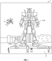
- FIG. 1 An augmented reality scene (1) is depicted wherein a user of an AR technology sees a real-world park-like setting (6) featuring people, trees, buildings in the background, and a concrete platform (1120).
- the user of the AR technology also perceives that he "sees" a robot statue (1110) standing upon the real-world platform (1120), and a cartoon-like avatar character (2) flying by which seems to be a personification of a bumble bee, even though these elements (2, 1110) do not exist in the real world.
- a robot statue 1110 standing upon the real-world platform (1120)
- a cartoon-like avatar character (2) flying by which seems to be a personification of a bumble bee even though these elements (2, 1110) do not exist in the real world.
- the human visual perception system is complex, it is challenging to produce a VR or AR technology that facilitates a comfortable, natural-feeling, rich presentation of virtual image elements amongst other virtual or real-world imagery elements.
- the invention relates to a system according to claim 1.
- Advantageous embodiments of the invention are the subject of the dependent claims.
- a display system in some embodiments, includes a waveguide; and an image injection device configured to direct a multiplexed light stream into the waveguide.
- the multiplexed light stream includes a plurality of light streams having different light properties.
- the waveguide includes in-coupling optical elements configured to selectively in-couple a first of the streams of light while being transmissive to one or more other streams of light.
- the waveguide is part of a stack of waveguides, which can include a second waveguide including in-coupling optical elements configured to selectively turn a second of the streams of light while being transmissive to one or more other streams of light.
- the in-coupling optical elements of the waveguide are configured to transmit at least one of the streams of light to the in-coupling optical elements of the second waveguide.
- liquid crystal devices including jet depositing liquid crystal material on a substrate and using an imprint pattern to align the molecules of the liquid crystal are described herein.
- devices including one or several layers of liquid crystal material can be manufactured.
- Liquid crystal devices manufactured using the methods described herein can include liquid crystal gratings including features and/or patterns that have a size less than about a few microns.
- Liquid crystal devices manufactured using the methods described herein can also include liquid crystal features and/or patterns that have a size less than the wavelength of visible light and may comprise what are referred to as Pancharatnam-Berry Phase Effect (PBPE) structures, metasurfaces, or metamaterials.
- PBPE Pancharatnam-Berry Phase Effect
- the small patterned features in these structures can be about 10 nm to about 100 nm wide and about 100 nm to about 1 micron high. In some cases, the small patterned features in these structures can be about 10 nm to about 1 micron wide and about 10 nm to about 1 micron high.
- Structures for manipulating light can include liquid crystal gratings with metasurface, otherwise referred to herein as metamaterials liquid crystal gratings or liquid crystal gratings with Pancharatnam-Berry Phase Effect (PBPE) structures.
- PBPE Pancharatnam-Berry Phase Effect
- Liquid crystal gratings with PBPE structures can combine the high diffraction efficiency and low sensitivity to angle of incidence of liquid crystal gratings with the high wavelength sensitivity of the PBPE structures.
- liquid crystal gratings with PBPE structures can be mass-produced which may not be possible using the existing methods of disposing PBPE structures on liquid crystal materials.
- the methods discussed herein can also be used to fabricate polarizers that are more transparent than existing polarizers.
- An innovative aspect of the subject matter disclosed herein includes a display system comprising a waveguide and an image injection device configured to direct a multiplexed light stream into the waveguide.
- the multiplexed light stream provided by the image injection device can comprise a plurality of light streams having different light properties.
- the waveguide comprises in-coupling optical elements that are configured to selectively in-couple a first of the streams of light while being transmissive to one or more other streams of light.
- the in-coupling optical elements can comprise at least one of diffractive structures, liquid crystal material, meta-surfaces, metamaterials, PBPE structures, liquid crystal polarization grating comprising PBPE structures or liquid crystal polarization grating comprising metasurface.
- the in-coupling optical elements can be switchable between transmissive and actively light redirecting states.
- Various embodiments of the waveguide can be included in an eyepiece of a head mounted display.
- the waveguide is a part of a stack of waveguides.
- the stack of waveguides can include a second waveguide comprising in-coupling optical elements that can be configured to selectively turn a second of the streams of light while being transmissive to one or more other streams of light.
- the in-coupling optical elements of the waveguide can be configured to transmit at least one of the streams of light to the in-coupling optical elements of the second waveguide.
- the light streams can have different wavelengths, different polarizations, or combinations thereof.
- the image injection device can be configured to simultaneously provide all of the light streams of the plurality of light streams to the waveguide.
- the image injection device can be configured to provide at least some of the light streams of the plurality of light streams to the waveguide at different times.
- the image injection device can be a scanning optical fiber.
- the image injection device can comprise a light modulating device.
- the waveguide and/or the second waveguide can comprise out-coupling elements that are configured to output the in-coupled first stream of light propagating in the waveguide.
- the out-coupling elements can comprise a first group of light redirecting elements configured to increase dimensions of an eyebox along at least one axis.
- the out-coupling element can further comprise a second group of light redirecting elements configured to increase dimensions of the eyebox along an axis that is orthogonal to the at least one axis.
- a display system comprising a plurality of stacked waveguides and an image injection device.
- the image injection device is configured to direct a multiplexed light stream into the plurality of stacked waveguides.
- the multiplexed light stream comprises a plurality of light streams having different light properties.
- Each waveguide in the plurality of stacked waveguides comprises in-coupling optical elements.
- Each waveguide is configured to selectively in-couple one or more of the plurality of light streams while being transmissive to one or more other of the plurality of light streams.
- the plurality of stacked waveguides can be included in an eyepiece of a head mounted display.
- Each waveguide comprises out-coupling elements that are configured to output the in-coupled one or more of the plurality of light streams propagating in the waveguide.
- the in-coupling optical elements can comprise at least one of diffractive structures, liquid crystal material, meta-surfaces, metamaterials, PBPE structures, liquid crystal polarization grating comprising PBPE structures or liquid crystal polarization grating comprising metasurface.
- the in-coupling optical elements can be switchable between transmissive and actively light redirecting states.
- the different light properties can have different wavelengths respectively, different polarizations respectively, or combinations thereof.
- the image injection device can be configured to simultaneously provide all of the light streams of the plurality of light streams to the waveguide.
- the image injection device can be configured to provide at least some of the light streams of the plurality of light streams to the waveguide at different times.
- the image injection device can be a scanning optical fiber.
- the image injection device can comprise a light modulating device.
- An innovative aspect of the subject matter disclosed herein includes a display system comprising a waveguide; and an image injection device configured to direct a multiplexed light stream into the waveguide.
- the multiplexed light stream can comprise a plurality of light streams having different light properties.
- the waveguide comprises first in-coupling optical elements configured to selectively in-couple a first of the stream of light while being transmissive to one or more other streams of light.
- the waveguide can comprise second in-coupling optical elements configured to selectively in-couple a second of the stream of light while being transmissive to one or more other streams of light.
- the waveguide can comprise third in-coupling optical elements configured to selectively in-couple a third of the stream of light while being transmissive to one or more other streams of light.
- the first, second or third in-coupling optical elements can include a liquid crystal layer comprising a metasurface.
- the waveguide can be included in an eyepiece of a head mounted display.
- Embodiments disclosed herein include optical systems, including display systems, generally.
- the display systems are wearable, which may advantageously provide a more immersive VR or AR experience.
- displays containing a stack of waveguides may be configured to be worn positioned in front of the eyes of a user, or viewer.
- two stacks of waveguides, one for each eye of a viewer may be utilized to provide different images to each eye.
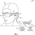
- FIG. 2 illustrates an example of wearable display system (80).
- the display system (80) includes a display (62), and various mechanical and electronic modules and systems to support the functioning of that display (62).
- the display (62) may be coupled to a frame (64), which is wearable by a display system user or viewer (60) and which is configured to position the display (62) in front of the eyes of the user (60).
- a speaker (66) is coupled to the frame (64) and positioned adjacent the ear canal of the user (in some embodiments, another speaker, not shown, is positioned adjacent the other ear canal of the user to provide for stereo/shapeable sound control).
- the display (62) is operatively coupled (68), such as by a wired lead or wireless connectivity, to a local data processing module (70) which may be mounted in a variety of configurations, such as fixedly attached to the frame (64), fixedly attached to a helmet or hat worn by the user, embedded in headphones, or otherwise removably attached to the user (60) (e.g., in a backpack-style configuration, in a belt-coupling style configuration).
- the local processing and data module (70) may comprise a processor, as well as digital memory, such as non-volatile memory (e.g., flash memory), both of which may be utilized to assist in the processing, caching, and storage of data.
- the data include data a) captured from sensors (which may be, e.g., operatively coupled to the frame (64) or otherwise attached to the user (60)), such as image capture devices (such as cameras), microphones, inertial measurement units, accelerometers, compasses, GPS units, radio devices, and/or gyros; and/or b) acquired and/or processed using remote processing module (72) and/or remote data repository (74), possibly for passage to the display (62) after such processing or retrieval.
- sensors which may be, e.g., operatively coupled to the frame (64) or otherwise attached to the user (60)
- image capture devices such as cameras
- microphones such as cameras
- inertial measurement units such as cameras
- accelerometers compasses
- GPS units GPS units
- the local processing and data module (70) may be operatively coupled by communication links (76, 78), such as via a wired or wireless communication links, to the remote processing module (72) and remote data repository (74) such that these remote modules (72, 74) are operatively coupled to each other and available as resources to the local processing and data module (70).
- the remote processing module (72) may comprise one or more processors configured to analyze and process data and/or image information.
- the remote data repository (74) may comprise a digital data storage facility, which may be available through the internet or other networking configuration in a "cloud" resource configuration. In some embodiments, all data is stored and all computations are performed in the local processing and data module, allowing fully autonomous use from a remote module.
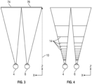
- FIG. 3 illustrates a conventional display system for simulating three-dimensional imagery for a user.
- Two distinct images 74 and 76, one for each eye 4 and 6, are outputted to the user.
- the images 74 and 76 are spaced from the eyes 4 and 6 by a distance 10 along an optical or z-axis parallel to the line of sight of the viewer.
- the images 74 and 76 are flat and the eyes 4 and 6 may focus on the images by assuming a single accommodated state.
- Such systems rely on the human visual system to combine the images 74 and 76 to provide a perception of depth for the combined image.
- Figure 4 illustrates aspects of an approach for simulating three-dimensional imagery using multiple depth planes.
- objects at various distances from eyes 4 and 6 on the z-axis are accommodated by the eyes (4, 6) so that those objects are in focus.
- the eyes 4 and 6 assume particular accommodated states to bring into focus objects at different distances along the z-axis. Consequently, a particular accommodated state may be said to be associated with a particular one of depth planes (14), such that objects or parts of objects in a particular depth plane are in focus when the eye is in the accommodated state for that depth plane.
- three-dimensional imagery may be simulated by providing different presentations of an image for each of the eyes (4, 6), and also by providing different presentations of the image corresponding to each of the depth planes.
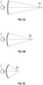
- Figs. 5A-5C illustrates relationships between distance and the divergence of light rays.
- the distance between the object and the eye (4) is represented by, in order of decreasing distance, R1, R2, and R3.
- R1, R2, and R3 As shown in Figs. 5A-5C , the light rays become more divergent as distance to the object decreases. As distance increases, the light rays become more collimated. Stated another way, it may be said that the light field produced by a point (the object or a part of the object) has a spherical wavefront curvature, which is a function of how far away the point is from the eye of the user.
- the human eye typically can interpret a finite of depth planes to provide depth perception. Consequently, a highly believable simulation of perceived depth may be achieved by providing, to the eye, different presentations of an image corresponding to each of these limited number of depth planes.
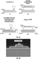
- FIG. 6 illustrates an example of a waveguide stack for outputting image information to a user.
- a display system 1000 includes a stack of waveguides, or stacked waveguide assembly, (178) that may be utilized to provide three-dimensional perception to the eye/brain using a plurality of waveguides (182, 184, 186, 188, 190).
- the display system (1000) is the system (80) of Figure 2 , with Figure 6 schematically showing some parts of that system (80) in greater detail.
- the waveguide assembly (178) may be integrated into the display (62) of Figure 2 .
- the waveguide assembly (178) may also include a plurality of features (198, 196, 194, 192) between the waveguides.
- the features (198, 196, 194, 192) may be lens.
- the waveguides (182, 184, 186, 188, 190) and/or the plurality of lenses (198, 196, 194, 192) may be configured to send image information to the eye with various levels of wavefront curvature or light ray divergence. Each waveguide level may be associated with a particular depth plane and may be configured to output image information corresponding to that depth plane.
- Image injection devices may be utilized to inject image information into the waveguides (182, 184, 186, 188, 190), each of which may be configured, as described herein, to distribute incoming light across each respective waveguide, for output toward the eye 4.
- a single beam of light e.g.
- a collimated beam may be injected into each waveguide to output an entire field of cloned collimated beams that are directed toward the eye (4) at particular angles (and amounts of divergence) corresponding to the depth plane associated with a particular waveguide.
- the image injection devices (200, 202, 204, 206, 208) are discrete displays that each produce image information for injection into a corresponding waveguide (182, 184, 186, 188, 190, respectively).
- the image injection devices (200, 202, 204, 206, 208) are the output ends of a single multiplexed display which may, e.g., pipe image information via one or more optical conduits (such as fiber optic cables) to each of the image injection devices (200, 202, 204, 206, 208).
- a controller 210 controls the operation of the stacked waveguide assembly (178) and the image injection devices (200, 202, 204, 206, 208).
- the controller 210 includes programming (e.g., instructions in a non-transitory medium) that regulates the timing and provision of image information to the waveguide (182, 184, 186, 188, 190) according to, e.g., any of the various schemes disclosed herein.
- the controller may be a single integral device, or a distributed system connected by wired or wireless communication channels.
- the controller 210 may be part of the processing modules (70 or 72) ( Figure 2 ) in some embodiments.
- the waveguides (182, 184, 186, 188, 190) may be configured to propagate light within each respective waveguide by total internal reflection (TIR).
- the waveguides (182, 184, 186, 188, 190) may each be planar, with major top and bottom surfaces and edges extending between those major top and bottom surfaces.
- the waveguides (182, 184, 186, 188, 190) may each include light redirecting elements (282, 284, 286, 288, 290) that are configured to redirect light, propagating within each respective waveguide, out of the waveguide to output image information to the eye 4.
- a beam of light is outputted by the waveguide at locations at which the light propagating in the waveguide strikes a light redirecting element.
- the light redirecting elements (282, 284, 286, 288, 290) may be reflective and/or diffractive optical features. While illustrated disposed at the bottom major surfaces of the waveguides (182, 184, 186, 188, 190) for ease of description and drawing clarity, in some embodiments, the light redirecting elements (282, 284, 286, 288, 290) may be disposed at the top and/or bottom major surfaces, and/or may be disposed directly in the volume of the waveguides (182, 184, 186, 188, 190). In some embodiments, the light redirecting elements (282, 284, 286, 288, 290) may be formed in a layer of material that is attached to a transparent substrate to form the waveguides (182, 184, 186, 188, 190).
- the waveguides (182, 184, 186, 188, 190) may be a monolithic piece of material and the light redirecting elements (282, 284, 286, 288, 290) may be formed on a surface and/or in the interior of that piece of material.
- each waveguide (182, 184, 186, 188, 190) is configured to output light to form an image corresponding to a particular depth plane.
- the waveguide (182) nearest the eye may be configured to deliver collimated light, as injected into such waveguide (182), to the eye (4).
- the collimated light may be representative of the optical infinity focal plane.
- the next waveguide up (184) may be configured to send out collimated light which passes through the first lens (192; e.g., a negative lens) before it can reach the eye (4); such first lens (192) may be configured to create a slight convex wavefront curvature so that the eye/brain interprets light coming from that next waveguide up (184) as coming from a first focal plane closer inward toward the eye (4) from optical infinity.
- first lens e.g., a negative lens
- the third up waveguide (186) passes its output light through both the first (192) and second (194) lenses before reaching the eye (4); the combined optical power of the first (192) and second (194) lenses may be configured to create another incremental amount of wavefront curvature so that the eye/brain interprets light coming from the third waveguide (186) as coming from a second focal plane that is even closer inward toward the person from optical infinity than was light from the next waveguide up (184).
- the other waveguide layers (188, 190) and lenses (196, 198) are similarly configured, with the highest waveguide (190) in the stack sending its output through all of the lenses between it and the eye for an aggregate focal power representative of the closest focal plane to the person.
- a compensating lens layer (180) may be disposed at the top of the stack to compensate for the aggregate power of the lens stack (198, 196, 194, 192) below.
- Such a configuration provides as many perceived focal planes as there are available waveguide/lens pairings.
- Both the light redirecting elements of the waveguides and the focusing aspects of the lenses may be static (i.e., not dynamic or electro-active). In some alternative embodiments, they may be dynamic using electro-active features.
- the light redirecting elements (282, 284, 286, 288, 290) may be configured to both redirect light out of their respective waveguides and to output this light with the appropriate amount of divergence or collimation for a particular depth plane associated with the waveguide.
- waveguides having different associated depth planes may have different configurations of light redirecting elements (282, 284, 286, 288, 290), which output light with a different amount of divergence depending on the associated depth plane.
- the light redirecting elements (282, 284, 286, 288, 290) may be volumetric or surface features, which may be configured to output light at specific angles.
- the light redirecting elements (282, 284, 286, 288, 290) may be volume holograms, surface holograms, and/or diffraction gratings.
- Light redirecting elements, such as diffraction gratings, are described in U.S. Patent Application No. 14/641,376, filed March 7, 2015 .
- the features (198, 196, 194, 192) may not be lenses; rather, they may simply be spacers (e.g., cladding layers and/or structures for forming air gaps).
- the light redirecting elements (282, 284, 286, 288, 290) are diffractive features that form a diffraction pattern, or "diffractive optical element" (also referred to herein as a "DOE").
- the DOE's have a relatively low diffraction efficiency so that only a portion of the light of the beam is deflected away toward the eye (4) with each intersection of the DOE, while the rest continues to move through a waveguide via total internal reflection.
- the light carrying the image information is thus divided into a number of related exit beams that exit the waveguide at a multiplicity of locations and the result is a fairly uniform pattern of exit emission toward the eye (4) for this particular collimated beam bouncing around within a waveguide.
- one or more DOEs may be switchable between "on” states in which they actively diffract, and "off” states in which they do not significantly diffract.
- a switchable DOE may comprise a layer of polymer dispersed liquid crystal, in which microdroplets comprise a diffraction pattern in a host medium, and the refractive index of the microdroplets can be switched to substantially match the refractive index of the host material (in which case the pattern does not appreciably diffract incident light) or the microdroplet can be switched to an index that does not match that of the host medium (in which case the pattern actively diffracts incident light).
- Figure 7 shows an example of exit beams outputted by a waveguide.
- One waveguide is illustrated, but it will be appreciated that other waveguides in the stack of waveguides (178) may function similarly.
- Light (400) is injected into the waveguide (182) at the input edge (382) of the waveguide (182) and propagates within the waveguide (182) by TIR.
- the DOE (282) At points where the light (400) impinges on the DOE (282), a portion of the light exits the waveguide as exit beams (402).
- the exit beams (402) are illustrated as substantially parallel but, as discussed herein, they may also be redirected to propagate to the eye (4) at an angle (e.g., forming divergent exit beans), depending on the depth plane associated with the waveguide (182).
- substantially parallel exit beams may be indicative of a waveguide that corresponds to a depth plane at a large distance (e.g., optical infinity) from the eye (4).
- Other waveguides may output an exit beam pattern that is more divergent, which would require the eye (4) to accommodate to a closer distance to bring it into focus on the retina and would be interpreted by the brain as light from a distance closer to the eye (4) than optical infinity.
- utilizing a dedicated image injection device (200, 202, 204, 206, or 208) for each waveguide (182, 184, 186, 188, or 190) may be mechanically complex and may require a large volume to accommodate all of the image injection devices and their related connections. A smaller form factor may be desirable for some applications, such as wearable displays.
- a smaller form factor may be achieved by using a single image injection device to inject information into a plurality of the waveguides.
- the image injection device delivers multiple image information streams (also referred to herein as information streams) to the waveguides, and these information streams may be considered to be multiplexed.
- Each waveguide includes in-coupling optical elements that interact with the information streams to selectively in-couple image information from a particular information stream into that waveguide.
- the in-coupling optical elements selectively redirect light from a particular information stream into its associated waveguide, while allowing light for other information streams to continue to propagate to other waveguides. The redirected light is redirected at angles such that it propagates through its associated waveguide by TIR.
- a single image injection device provides a multiplexed information stream to a plurality of waveguides, and each waveguide of that plurality of waveguides has an associated information stream that it selectively in-couples using in-coupling optical elements.
- each information stream may be formed by light of different colors (different wavelengths) and/or different polarizations (preferably different circular polarizations).
- the in-coupling optical elements are configured to selectively redirect light of a particular polarization and/or of one or more particular wavelengths, thereby allowing a specific correspondence, e.g., one-to-one correspondence, between an information stream and a waveguide.
- the in-coupling optical elements are diffractive optical elements configured to selectively redirect light based upon the properties of that light, e.g., the wavelength and/or polarization of that light.
- each image injection device provides image information to a plurality of two, three, four, or more waveguides by providing, respectively, two, three, four, or more information streams to that plurality of waveguides.
- multiple such image injection devices may be used to provide information to each of multiple pluralities of waveguides.
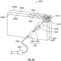
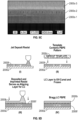
- a stack 3000 includes waveguides 3002 and 3004, which include in-coupling optical elements 3012 and 3014, respectively.
- the waveguides 3002 and 3004 may be substantially planar plates, each having a front and rear major surface and edges extending between these front and rear major surfaces.
- waveguide 3002 has front major surface 3002a and rear major surface 3002b.
- the major surfaces of the waveguides may include a cladding layer (not illustrated) to facilitate the TIR of light within each waveguide.
- the stack 3000 of waveguides corresponds to the stack 178 of Figure 6 and may be utilized to replace the stack 178 in the display systems disclosed herein
- light streams A and B have different light properties, e.g., different wavelengths and/or different polarizations (preferably different circular polarizations).
- the light streams A and B include distinct image information streams.
- Light A and B and their information streams are propagated through optical conduit 3024 (e.g., an optical fiber) as a multiplexed information stream to an image injection device 3021.
- the image injection device injects light 3040 (containing the multiplexed information stream as combined light streams A and B) into the waveguide stack 3000.
- the image injection device 3021 includes an actuator 3020 (such as a piezoelectric actuator) that is coupled to an optical fiber 352, which may be used to scan the fiber tip of the fiber 352 across an area of the stack 3000. Examples of such scanning fiber image injection devices are disclosed in U.S. Patent Application No. 14/641,376, filed March 7, 2015 .
- the image injection device 3021 may be stationary and, in some embodiments, may direct light towards the stack 3000 from multiple angles.
- each waveguide includes in-coupling optical elements.
- waveguide 3002 includes in-coupling optical elements 3012
- waveguide 3004 includes in-coupling optical elements 3014.
- the in-coupling optical elements 3012 and 3014 are configured to selectively redirect one of light streams A and B.
- in-coupling optical elements 3012 may selectively redirect at least a portion of light stream A to in-couple that light stream into the light guide 3002.
- the in-coupled portion of light stream A propagates through the waveguide 3002 as light 3042.
- the light 3042 propagates through the waveguide 3002 by TIR off the major surfaces 3002a and 3002b of that waveguide.
- in-coupling optical elements 3014 may selectively redirect at least a portion of light stream B to in-couple that light stream into the light guide 3004.
- the in-coupled portion of light stream B propagates through the waveguide 3004 as light 3044.
- the light 3044 propagates through the waveguide 3004 by TIR off the major surfaces 3004a and 3004b of that waveguide.
- the multiplexed light stream 3040 includes both light streams A and B simultaneously, and light stream A may be in-coupled to waveguide 3002 while light stream B is in-coupled to waveguide 3004, as discuss above.
- light streams A and B may be provided to the waveguide stack 3000 at different times. In such embodiments, only a single waveguide may be utilized to receive these information streams, as discussed herein. In either case, the light streams A and B may be coupled to the optical conduit 3024 by the optical coupler 3050. In some embodiments, the optical coupler 3050 may combine light streams A and B for propagation through the optical conduit 3024.
- optics 3030 may be disposed between the image injection device 3021 and the in-coupling optical elements 3012 and 3014.
- the optics 3030 may include, e.g., lens that facilitating directing light rays onto the various in-coupling optical elements 3012 and 3014, e.g., by focusing the light onto in-coupling optical elements 3012 and 3014.
- the optics are part of the image injection device 3021 and may be, e.g., a lens at the end of the image injection device 3021.
- optics 3030 may be omitted completely.
- the in-coupling optical elements 3012 and 3014 are configured to selectively redirect the light streams A and B based upon one or more light properties that differ between those light streams.
- light stream A may have a different wavelength than light stream B and the in-coupling optical elements 3012 and 3014 may be configured to selectively redirect light based on wavelength.
- the different wavelengths correspond to different colors, which can improve the selectivity of the in-coupling optical elements relative to using different wavelengths of the same color.
- light stream A may have a different polarization than light stream B and the in-coupling optical elements 3012 and 3014 may be configured to selectively redirect light based on polarization.
- the in-coupling optical elements 3012 and 3014 may be configured to selectively redirect light based on polarization.
- the light streams A and B have different circular polarization.
- the light streams A and B may have multiple differences in light properties, including, e.g., both different wavelengths and different polarizations.
- in-coupling optical elements 3012 and 3014 are diffractive optical elements, including diffractive gratings (e.g., a grating comprising liquid crystal such as a liquid crystal polarization grating).
- the optical element may include a meta-surface (e.g., comprise a PBPE), such as a surface have a pattern with feature sizes on the order of one's or tens of nanometers.
- suitable in-coupling optical elements 3012 and 3014 include the optical elements 2000b, 2000d ( Figure 9A ) and the optical elements of Figures 9E-9H .
- such optical elements are highly efficient at selectively redirecting light of different polarizations and/or different wavelengths.
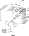
- the stack 3000 can include more than two waveguides, e.g., 4, 6, 8, 10, 12, or other numbers of waveguides, so long as image information can be adequately provided to individual waveguides and to a user's eyes through the stack 3000.
- the illustrated stack 3000 includes waveguides 3006 and 3008 in addition to the waveguides 3002 and 3004.
- the waveguides 3006 and 3008 include in-coupling optical elements 3012 and 3014, respectively.
- the waveguides 3002, 3004, 3006, and 3008 may be similar, except for the in-coupling optical elements, which may each be configured to redirect and in-couple light having different light properties.
- in-coupling optical elements for multiple waveguides may be similar. It will be appreciated that all the disclosure herein related to Figure 8A apply to Figure 8B , except that the number of waveguides in Figure 8B is greater than in Figure 8A .
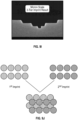
- light streams A, B, C, and D have different light properties, e.g., different wavelengths and/or different polarizations (preferably different circular polarizations).
- light streams A, B, C, and D may each include light of different wavelengths.
- various combinations of different wavelengths and polarizations are possible.
- a and B may have similar wavelengths and different polarizations
- C and D may have similar wavelengths and different polarizations, with A and B different from C and D.
- Light streams A, B, C, and D are propagated through optical conduit 3024 as a multiplexed information stream to the image injection device 3021, which injects light 3040 of the multiplexed information stream into the waveguide stack 3000.
- the multiplexed information stream may include all light streams simultaneously, or one or more of the light streams may be directed to the stack 3000 at different times.
- each waveguide includes in-coupling optical elements that selectively in-couple light into that waveguide.
- waveguide 3002 includes in-coupling optical elements 3012, which may be configured to in-couple light stream A into that waveguide, so that it propagates by TIR in that waveguide as light 3042; waveguide 3004 includes in-coupling optical elements 3014, which may be configured to in-couple light stream B into that waveguide, so that it propagates by TIR in that waveguide as light 3044; waveguide 3006 includes in-coupling optical elements 3016, which may be configured to in-couple light stream C into that waveguide, so that it propagates by TIR in that waveguide as light 3046; and waveguide 3008 includes in-coupling optical elements 3018, which may be configured to in-couple light stream D into that waveguide, so that it propagates by TIR in that waveguide as light 3048.
- a single light stream (e.g., light stream A, B, C, or D) may be in-coupled to a single waveguide.
- multiple light streams may be in-coupled to the same waveguide.
- the light streams are in-coupled at different times.
- such temporally separated in-coupling may be achieved using in-coupling optical elements that selectively turn light based on multiple different light properties (e.g., multiple different wavelengths or multiple different polarizations), while the image injection device provides the information streams for a particular waveguide at different times.
- both light streams A and B may be in-coupled to waveguide 3002, with the in-coupling optical elements 3012 selectively in-coupling light streams A and B while allowing light streams C and D to pass through, and with the light streams A and B providing light to the in-coupling optical elements 3012 at different times while simultaneously providing light streams C and/or D to the in-coupling optical elements 3012.
- one or more other waveguides may be similarly configured to in-couple multiple light streams to those waveguides.
- multiple light streams may be provided simultaneously to the in-coupling optical elements (e.g., in-coupling optical elements 3012), and the in-coupling optical elements may be configured to change states to choose between in-coupling light stream A or B.
- the in-coupling optical elements may be a grating formed of liquid crystal material disposed between electrodes (e.g., transparent electrodes such as ITO).
- the liquid crystal may change states (e.g., orientations) with the application of a voltage potential, with one state configured to selectively in-couple one light stream (e.g., light stream A) and another state configured to be transparent to all light streams (e.g., both light stream A and B).
- another layer of switchable liquid crystal material, forming a different grating may be provided between electrodes, with one state configured to selectively in-couple a different light stream (e.g., light stream B) and another state configured to be transparent to all light streams (e.g., both light stream A and B).
- both types of liquid crystal material may be disposed on the same level, but in different areas.
- the liquid crystal material may be configured such that when one type of material is transparent to the light streams, the other type selectively in-couples light of a particular light stream, and vice versa.
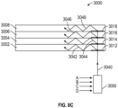
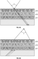
- FIG. 8C a top-down schematic view of the display system of Figure 8B is illustrated.
- the top-down view is taken looking down along a top edge of the stack 3000 of Figure 8B .
- portions of multiplexed light stream 3040 are selectively in-coupled into each of waveguides 3002, 3004, 3006, and 3008 as in-coupled light 3042, 3044, 3046, and 3048.
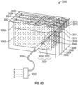
- the waveguides may include light redirecting elements (e.g., light redirecting elements (282, 284, 286, 288, 290)) that output or out-couple light, which has been propagating inside the waveguide, so that the out-coupled light propagates towards the eyes 4 of a viewer ( Figure 6 ).
- Figure 8D illustrates the display system of Figure 8C , with light redirecting elements to out-couple light from each waveguide.
- waveguide 3002 includes out-coupling light redirecting elements 3062
- waveguide 3004 includes out-coupling light redirecting elements 3064
- waveguide 3006 includes out-coupling light redirecting elements 3066
- waveguide 3008 includes out-coupling light redirecting elements 3068.
- out-coupling light redirecting elements may include different groups of light redirecting elements, each of which functions differently.
- out-coupling light redirecting elements 3062 may include a first group of light redirecting elements 3062a and a second group of light redirecting elements 3062b.
- light redirecting elements 3062b may be exit pupil expanders (EPEs; to increase the dimensions of the eye box in at least one axis)
- light redirecting elements 3062a may be orthogonal pupil expanders (OPEs; to increase the eye box in an axis crossing, e.g., orthogonal to, the axis of the EPEs).
- EPEs and OPEs are disclosed in U.S. Provisional Patent Application No. 62/005,807, filed May 30, 2014 .
- images are formed by the waveguides using information streams with encoded x-y pixel information.
- the information streams of different colors may each indicate the intensity of light for a particular location on an x-y grid corresponding to the x-y pixel information for the image.
- the matching of information streams to waveguides is achieved using the properties of light and is not necessarily dependent upon the x-y pixel information provided by that light. Consequently, the x-y pixel information may be encoded at any suitable location using any suitable device along the path of the light before the light impinges on the in-coupling optical elements 3012, 3014, 3016, and 3018.
- a light source e.g., LED or OLED
- the desired light properties e.g., desired wavelengths and/or polarizations
- an information stream may be formed having both the desired light properties and encoded x-y pixel information as it is emitted from the light source.
- light having the desired light properties is passed through a light modulation device in which the x-y pixel information is encoded.
- Figure 8E illustrates the display system of Figure 8B and shows a light modulation device 3070 for providing x-y pixel information to the image information stream.
- the light modulation device 3070 may be part of the image injection device 3021, and may be configured to provide image information using a scanning fiber, or one or more stationary aperture display devices for providing image information to the waveguides.
- the light modulation device 3070 modifies the light as it passes through the device (e.g., the intensity of the light may be modified by being passed through pixel elements having controllable variable light transmission).
- the light modulation device may modify light by selectively redirecting (e.g., reflecting) light to propagate into the waveguide stack 3000. Examples of light modulation devices include transmissive liquid crystal displays and micro-mirror devices (such as a "digital light processing", or "DLP" system, such as those available from Texas Instruments, Inc.).
- This section relates to liquid crystals, polarization gratings, and Pancharatnam-Berry Phase Effect (PBPE) structures, methods of fabrication thereof as well as other structures and methods.
- methods and apparatus are provided for manufacturing liquid crystal grating structures that have high diffraction efficiency, low sensitivity to angle of incident and high wavelength sensitivity.
- Various methods described herein include disposing a layer of liquid crystal material using inkjet technology and using an imprint template to align the liquid crystal material.
- the liquid crystals, polarization gratings, and Pancharatnam-Berry Phase Effect (PBPE) structures disclosed in this Part II may be utilized to form light redirecting elements for the various waveguides of the waveguide stacks 178 ( Figure 6 ) or 3000 ( Figures 8A-8E ).
- PBPE Pancharatnam-Berry Phase Effect
- such liquid crystals, polarization gratings, and Pancharatnam-Berry Phase Effect (PBPE) structures may advantageously be applied to form the various in-coupling optical elements disclosed herein, including the in-coupling optical elements 3012, 3014, 3016, and/or 3018 ( Figure 8A-8E ).
- a variety of imaging systems and optical signal processing systems can include liquid crystal devices to control/manipulate an optical wavefront, wavelength, polarization, phase, intensity, angle and/or other properties of light.
- Liquid crystals are partly ordered materials whose molecules are often shaped like rods or plates or some other forms that can be aligned along a certain direction. The direction along which the molecules of the liquid crystal are oriented can be manipulated by application of electromagnetic forces which can be used to control/manipulate the properties of light incident on the liquid crystal material.
- the following detailed description is directed to certain embodiments for the purposes of describing the innovative aspects.
- teachings herein can be applied in a multitude of different ways.
- the innovative aspects may be implemented in any optical component or device that is configured to manipulate one or more characteristics of incident light.
- a layer of liquid crystal material is deposited on a substrate using jet deposition technology (e.g., inkjet technology).
- Jet deposition technology e.g., inkjet technology
- Surface relief features e.g., PBPE structures
- the surface relief features may be configured (e.g., with particular spacing and/or heights) to achieve particular light redirecting properties.
- imprinting can be repeated on different levels to produce successive layered cross-sections that, in combination, can behave as volumetric features such as exists in "bulk" volume-phase materials and devices.
- these surface relief features can be modeled as "Bragg" structures.
- such structures can be used to produce binary surface-relief features in which there exists a material-to-air interface, resist-to-air interface, resin-to-air interface or a liquid crystal material-to-air interface that produces diffraction, or a material-to-lower index resist interface, resist-to-lower index resist interface, resin-to-lower index resist interface or a liquid crystal material-to-lower index resist interface that does the same.
- the gratings can be modeled as "raman-nath” structures, rather than Bragg structures.
- the molecules of the liquid crystal material are aligned through the process of imprinting due to the physical shape of the nanostructures and their electrostatic interaction with the liquid crystal (LC) material. Alignment of the liquid crystal layer using the imprint pattern is discussed in greater detail below.
- a layer of material, (e.g., a polymer), to serve as a photo-alignment layer may be deposited using jet deposition technology (in which a jet or stream of material is directed onto a substrate), e.g., via ink-jet onto a substrate or pre-coated substrate.
- the photo-alignment layer is patterned by nano-imprinting using a template incorporating the desired LC orientation pattern.
- this pattern is a PBPE pattern
- the template, comprising a physical relief may be made with interferometric and/or lithographic techniques. The template is lowered on to the soft polymer resin and UV light is used to cure the resin to a fixed state.
- capillary action fills the template with the polymer material before it is cured.
- the template is retracted, leaving the patterned, cured resin in place on the substrate.
- a second step, using a deposition process e.g., jet or spin coating
- applies a layer of LC e.g., LC suspended in resin
- the LC aligns to the photo-alignment layer pattern below it, and when this occurs, the resin is fixed in place using UV light, heat, or a combination of both.
- LC suspended in solvent e.g., resin
- the template containing the nanoimprint pattern e.g., a PBPE pattern
- the LC material is fixed in place using a cure process (e.g., UV, heat or a combination of both).
- a cure process e.g., UV, heat or a combination of both.
- the resulting structure may be used directly as a functional element, or in some cases, a low refractive index material can be deposited over the imprinted liquid crystal material to fill the interstitial areas between the surface features imprinted in the liquid crystal material.
- the low refractive index material can be configured as a planarization layer by tuning the viscoelastic and chemical properties of the liquid crystals based resist (e.g., a liquid crystal polymer or a resin comprising a liquid crystal) or by contacting the top surface of the low refractive index material with a planarization imprint template (e.g., a template having a substantially planar surface).
- the low refractive index material can be planarized by a chemical and/or mechanical planarization process.
- the planarization process is preferably chosen to form a planarized surface that is smooth, to reduce optical artifacts that may be caused by a rough surface. Additional layers such as additional liquid crystal layers can be deposited using the jet technology over the liquid crystal layer.
- the PBPE structures in the different layers of liquid crystal can be configured to diffract, steer, and/or disperse or combine different wavelengths of light. For example, red, green and blue wavelengths can be diffracted, dispersed, or redirected along different directions by the PBPE structures in the different liquid crystal layers.
- the different liquid crystal layers are preferably formed with materials that provide sufficient structural stability and adhesion to allow layers to be stacked over one another.
- organic or inorganic imprint resist materials including polymerizable materials that form optically transmissive cured structures, may be used.
- the liquid crystal layers can include an acrylic liquid crystal formulation. Acrylic liquid crystal layers can provide adhesive properties that facilitate the stacking of layers on top of each other.
- both the liquid crystal material and the low refractive index material may be flowable materials.
- these materials may be subjected to a process to immobilize them after contact with the imprint templates and before removing the contacting template.
- the immobilization process may include a curing process, as discussed herein.
- a layer of a photoresist material (e.g., a resin or a polymer) is deposited on a substrate.
- the deposition may be accomplished by various deposition methods, including spin coating. More preferably, in some embodiments, the deposition is accomplished using jet technology (e.g., inkjet technology).
- the photoresist is imprinted with an imprint template or mold having surface relief features (e.g., PBPE structures).
- a layer of liquid crystal material can be deposited using jet technology on the imprinted layer of photoresist.
- the imprinted photoresist layer can serve as an aligning layer to align the molecules of the liquid crystal material as it is deposited. Additional layers such as additional liquid crystal layers or layers not comprising liquid crystal can be deposited using the jet technology over the liquid crystal layer.
- a planarization layer can be deposited over the deposited liquid crystal layer.
- liquid crystal materials such as, for example, doped liquid crystal, un-doped liquid crystal, and other non-liquid crystal materials can be deposited using inkjet technology.
- Inkjet technology can provide thin controlled (e.g., uniform) thickness of the deposited liquid crystal layer or planarization layer.
- Inkjet technology can also provide layers of different thickness such as layers of liquid crystal or other layers having a different thickness in different areas on the surface and can accommodate different pattern height and keep a constant residual layer thickness underneath the imprinted patterns.
- Inkjet technology is advantageously capable of providing thin layers, for example between about 10 nm and 1 micron; or between about 10 nm and about 10 microns in thickness and can reduce waste in comparison with other techniques such as spin coating.
- inkjet technology can facilitate deposition of different liquid crystal compositions on the same substrate.
- inkjet nano-imprinting can produce a very thin residual layer thickness.
- the uniform area below the imprint pattern can correspond to the residual layer.
- PBPE and other diffractive structures can exhibit variable and sometimes enhanced performance with very thin or zero residual layer thickness.
- Inkjet nano-imprinting approaches can be used to deposit different types of materials across a given substrate simultaneously, and can be used to produce variable thickness materials in different areas of a single substrate simultaneously. This may be beneficial to PBPE structures, particularly when they are combined in a single substrate with more conventional diffractive structures which may require other materials and/or thicknesses of resist.
- the liquid crystal layers deposited by jet technology can be cured using UV curing, thermal methods, freezing, annealing and other methods.
- the imprint template can include complex groove geometries (e.g., grooves with multiple steps, gratings with different orientations, etc.).
- Liquid crystal devices manufactured using the methods described herein can include liquid crystal layers comprising gratings with different orientations and different PBPE structures.
- the manufacturing methods using inkjet technology described herein can also be configured to manufacture polarizers having increased transmissivity and/or wave plates comprising subwavelength features and/or metamaterials. These and other aspects are discussed in detail below.
- Figure 9A illustrates an embodiment of a method of fabricating a liquid crystal device, preferably using inkjet technology.
- a layer 2000b of liquid crystal material is deposited on a substrate 2000a, e.g., using inkjet technology, as shown in panel (i).
- the liquid crystal material can include a doped or an un-doped liquid crystal material.
- the liquid crystal material can be a polymer stabilized nematic liquid crystal material.
- the substrate 2000a can include glass, plastic, sapphire, a polymer or any other substrate material.
- the layer 2000b of the liquid crystal material can have a thickness between about 20 nanometers and 2 microns. In some embodiments, the layer 2000b of the liquid crystal material can have a thickness between about 0.5 microns and about 10 microns.
- the layer 2000b of the liquid crystal material can be imprinted with an imprint pattern 2000c including wavelength and sub-wavelength scale surface features, as shown in panel (ii).
- the surface features can include PBPE structures that can directly manipulate the phase of the incoming light. Without any loss of generality, a PBPE structure can be thought of as a type of polarization grating structure.
- the imprint pattern 2000c can include an array of grooves comprising PBPE structures.
- the array of grooves can form a liquid crystal grating structure that can have high diffraction efficiency and low sensitivity to incident angle.
- the grooves can have a depth between about 20 nm and about lmicron and a width between about 20 nm and about 1 micron.
- the grooves can have a depth between about 100 nm and about 500 nm and a width between about 200 nm and about 5000 nm. In some embodiments, the grooves can have a depth between about 20 nm and about 500 nm and a width between about 10 nm and about 10 microns.
- the PBPE structures can include sub-wavelength patterns that encode phase profile directly onto the local orientation of the optical axis.
- the PBPE structures can be disposed on the surface of the liquid crystal grating structures.
- the PBPE structures can have feature sizes between about 20 nm and about 1 micron. In some embodiments, the PBPE structures can have feature sizes between about 10 nm and about 200 nm.
- the PBPE structures can have feature sizes between about 10 nm and about 800 nm.
- an underlying PBPE structure can be used as an alignment layer for volumetric orientation of LC. The volumetric component in this case happens automatically, as the LCs naturally align themselves to the alignment layer.
- the imprint pattern 2000c can include a simple geometric pattern, such as, for example, a plurality of grooves or more complicated pattern such as multi-tier geometry including a plurality of grooves and recesses as shown in figure 9B .
- the imprint pattern 2000c can include a plurality of imprint layers, each imprint layer including a different imprint pattern as shown in figure 9C .
- the imprint layers 2000c-1, 2000c-2 and 2000c-3 include a plurality of grooves with progressively decreasing space between adjacent grooves.
- the imprint pattern can include patterns such as chevron, spirals, arcs, etc.
- the imprint pattern can be fabricated on a semiconductor material or other structure using methods such as e-beam lithography or other lithography methods.
- the layer 2000b of the liquid crystal material is aligned to the imprinted pattern.
- the spaces between adjacent grooves can be filled with a material 2000d.
- filling material may comprise a transparent material having a lower refractive index less than the refractive index of the liquid crystal material, as shown in panel (iii).
- Such a configuration can be used, for example, in a waveguide structure. In this manner a high refractive index difference can be obtained between the liquid crystal grating structures and its surrounding such that the liquid crystal gratings can have high diffraction efficiency.
- the PBPE LC grating may be made with a material-to-air interface, a resist-to-air interface, resin-to-air interface or liquid crystal material-to-air interface, where air is the low index "material".
- the liquid crystal gratings can be configured as Bragg liquid crystal gratings.
- the layer of low refractive index material 2000d can be configured as a planarization layer.
- the layer of low refractive index material 2000d can be configured to be planarized by another imprint pattern 2000e, as shown in panel (iv).
- Figure 9D illustrates another embodiment of a method of fabricating a liquid crystal device, preferably using inkjet technology.
- a layer 2000f of a resist is deposited on a substrate 2000a using inkjet technology, as shown in panel (i).
- the resist can include materials such as, for example, organic and inorganic based imprint materials, resins or polymers.
- the resist can include materials disclosed in U.S. Patent No. 8,076,386 .
- the resist layer 9F can have a thickness between about 20 nm and about 1 micron. In some embodiments, the resist layer 9F can have a thickness between about 10 nm and about 5 microns.
- the resist layer 2000f can be imprinted with an imprint pattern 2000c including volume and/or surface features, as shown in panel (ii).
- a layer 2000b of liquid crystal material can be disposed by inkjet on the imprinted resist layer 2000f, as shown in panel (iii).
- the imprinted resist layer can serve to align the liquid crystal material as it is jet deposited onto the imprinted resist layer 2000f.
- liquid crystal devices fabricated using above described methods can be cured using UV curing, thermal curing, freezing or other curing methods.
- Another embodiment of a method to fabricate liquid crystal devices includes imprinting a desired alignment structure in UV curable resist using Jet and Flash TM Imprint Lithography (J-FIL); and dispensing a liquid crystal polymer formulation from inkjet.
- the liquid crystal polymer can have a high solvent content, for example, to provide sufficiently low viscosity to enable efficient egress through the inkjets.
- the liquid crystal polymer can be in an isotropic state as it is dispensed.
- the liquid crystal polymer can be configured to align along the alignment structure in the resist by driving off the solvent. Additional liquid crystal polymer layers can be disposed on top of the disposed liquid crystal polymer layer by following the method described above. The formulation and the viscosity of the liquid crystal material in the solvent may also be adjusted to achieve rapid drying process for the dispensed liquid crystal materials.
- Figures 9E-9H illustrate embodiments of liquid crystal gratings fabricated using the methods described above.
- Figure 9E illustrates a single layer liquid crystal grating including PBPE structures that have high diffraction efficiency, high wavelength sensitivity and low sensitivity to incident angle.
- the liquid crystal gratings illustrated in Figure 9E can be manufactured using the process depicted in Figure 9A .
- a liquid crystal polymer LCP1 can be deposited on a substrate and an imprint template can be used to imprint a pattern on the liquid crystal polymer LCP1 such that the molecules of the liquid crystal polymer LCP1 are self-aligned to the imprinted pattern.
- the pattern can include a metasurface (e.g., PBPE structures).
- Figure 9F illustrates a liquid crystal grating including PBPE structures that have high diffraction efficiency, high wavelength sensitivity and low sensitivity to incident angle.
- the liquid crystal gratings can be manufactured using the process depicted in Figure 9D .
- an alignment layer comprising a polymer (e.g., a resist or a resin) can be deposited on a substrate and an imprint template can be used to imprint a pattern on the polymer.
- a layer of liquid crystal material is deposited on the alignment layer such that the molecules of the liquid crystal layer are aligned to the pattern imprinted on the alignment layer.
- the pattern can be part of a metasurface (e.g., PBPE structures).
- PBPE structure of the first liquid crystal layer (LCP1) can serve as the alignment structure for the second liquid layer (LCP2).
- Figure 9G illustrates a three-layer liquid crystal grating including PBPE structures that have high diffraction efficiency, high wavelength sensitivity and low sensitivity to incident angle.
- the multilayer liquid crystal gratings can be manufactured using the processes depicted in Figures 9A or 9D .
- the multi-layer liquid crystal gratings illustrated in Figure 9G can be manufactured by aligning the molecules of a first liquid crystal layer (LCP1) using a first alignment layer comprising a first imprint pattern deposited on the substrate, aligning the molecules of a second liquid crystal layer (LCP2) using a second alignment layer comprising a second imprint pattern deposited on the first alignment layer and aligning the molecules of a third liquid crystal layer (LCP3) using a third alignment layer comprising a third imprint pattern deposited on the second alignment layer.
- the process of Figure 9A may be utilized to form one or more of the first, second, and third liquid crystal layers have aligned liquid crystal molecules (LCP1, LCP2, and LCP3, respectively).
- each of LCP1, LCP2, and LCP3 may be formed by imprinting a pattern in a liquid crystal layer deposited over the substrate.
- the imprinting may be accomplished using an imprint template having a pattern that causes the liquid crystal molecules to align to the pattern.
- the imprint template may subsequently be removed and a filler may be deposited into the gaps left by the imprint template removal.
- the first, second and third imprint patterns can each be a metasurface (e.g., PBPE structures).
- the first, second and third imprint patterns can be different such that each imprint pattern is configured to selectively diffract/redirect different wavelengths of light in an incident beam to couple each of the different wavelengths in one or more waveguides.
- the different wavelengths of light in an incident beam can be coupled into the one or more waveguides at the same angle.
- the different wavelengths of light in an incident beam can be coupled into the one or more waveguides at different wavelengths.
- the PBPE structure of the first liquid crystal layer (LCP1) can serve as the alignment structure for the second liquid layer (LCP2) which in turn can serve as the alignment structure for the third liquid layer (LCP3).
- the embodiment illustrated in Figure 9G can include different PBPE structures such that different wavelengths of light in an incident beam of light are diffracted or redirected at different output angles such that they are spatially separated.
- the incident beam of light can be monochromatic or polychromatic.
- the multi-layer liquid crystal structure can be used to combine different wavelengths of light as illustrated in Figure 9H .
- Figure 9I illustrates a cross-section of a resist layer imprinted with an imprint pattern illustrated in figure 9B .
- the liquid crystal layer can be formed with a variety of materials.
- an acrylate liquid crystal formulation can be disposed over the polymer align imprint structure using inkjet and imprint technology.
- Acrylate composition can facilitate stacking different liquid crystal layers on top of each other that can adhere to each other without adhesive layers thereby making process simpler.
- Different liquid crystal layers can be stacked to achieve a desired effect, for example, the desired polarization, diffraction, steering, or dispersion effect.
- the method described above can be used to fabricate liquid crystal polarization gratings and patterned guiding layers using linear sub masters with jet dispensing technology (e.g., J-FIL).
- Different liquid crystal grating structures can be fabricated by combining structure with different shapes, orientations, and/or pitches. This process is described in more detail with reference to Figure 9J which illustrates a first imprint structure having discrete droplets or sections that are oriented along a first direction and a second imprint structure having discrete droplets or sections that are oriented along a second direction.
- the discrete droplets or sections of the first and the second imprint structures can be dispersed using inkjet technology.
- the discrete droplets or sections of the first and the second imprint structures can merge or not merge in different embodiments.
- the discrete droplets or sections in the first and the second imprint structures can be combined to produce an imprint structure with discrete droplets or sections having different orientations.
- Liquid crystal material can be disposed on the combined imprint pattern to produce liquid crystal gratings with molecules aligned along different orientations.
- the different orientations of the separate sections together can produce a more complex grating pattern, similar, for example, to that of a PBPE, in the aggregate.
- the inkjet and imprint methods discussed herein can be used to fabricate other optical elements such as waveguide plates, optical retarders, polarizers, etc.
- a polarizer that is more transparent than existing polarizers can be fabricated using the methods described herein.
- the method includes disposing a transparent or substantially transparent material that is patterned such as a polymer imprint and depositing a polarizer material, such as, for example, an iodine solution containing dichroic dye.
- the method includes imprinting a pattern on the transparent polymer.
- the pattern can be linear grooves, chevrons, spirals, arcs, or any other simple or complicated pattern.
- the pattern can be a periodic linear grating structure.
- the polarizer material can then be deposited on the patterned transparent polymer using the jet technology (such as, for example, J-FIL) described above, imprint planarization or by spin coating.
- Figure 9K and 9L illustrate different polarizer configurations that can be fabricated using the methods described above.
- the polarizers fabricated using the technology described herein can be more transparent than existing polarizers. Such a component may be useful for devices that utilize low extinction ratio polarizers such as a waveguide stack for head mounted display eyepieces for augmented and virtual reality as described elsewhere herein.
- Subwavelength scale grating structures can induce birefringence in materials.
- single dimensional grating can act as artificial negative uniaxial materials whose optical axes are parallel to the grating vector.
- Such birefringence can be referred to as form birefringence.
- substrates including subwavelength scale grating structures can function as wave plates.
- the amount of retardation provided by substrates including subwavelength scale grating structures can depend on the dimension (e.g., height, width, pitch, etc.) of the grating patterns as well as the material refractive index.
- a material with higher index comprising a pattern of subwavelength scale features can provide higher retardation than a material with lower index comprising a similar pattern of subwavelength scale features.
- Inkjet and imprint technology such as, for example, J-FIL allows high throughput Ultra Violet Nano-Imprint Lithography (UV-NIL) patterning capabilities with very low waste of material over any defined area.
- Inkjet and imprint technology such as, for example, J-FIL can also facilitate repeated stacking of imprinted layers.
- Imprint layers single or multi-layered with such subwavelength scale grating structures with or without varying geometry / orientation can provide varying degrees of phase-shift.
- Embodiments of patterned birefringent materials can enhance thin film integration capabilities in various optical applications.
- the polarization of light output from substrates including subwavelength scale grating structures can depend on the orientation, shape and/or pitch of the subwavelength scale grating structures.
- Embodiments of wave plates including subwavelength scale grating structures can also be fabricated using the inkjet and imprint methods described herein.
- Figure 9M illustrates an embodiment of a waveguide plate 2005 having a light entrance surface 2006 and a light exit surface 2007.
- the waveguide plate 2005 can include a plurality of subwavelength scale grating features with varying shapes, orientations and/or pitches such that incident unpolarized light is output as a polarized light.
- the wave plate 2005 can include multiple stacks of thin transparent films 2009a, 2009b and 2009c that are imprinted with subwavelength scale grating features with varying shapes, orientations and/or pitches.
- the grating features can be imprinted on the transparent films using an imprint template as shown in Figure 9C .
- the transparent films 2009a, 2009b and 2009c can comprise imprintable resists having refractive index between about 1.45 and 1.75.
- the polarization of the light output from a multilayer structure can depend on the shapes, orientations and/or pitches of the grating structures as well as refractive index difference between the different layers.
- incident unpolarized light is converted to right circularly polarized light by the waveguide plate 2005.
- the waveguide plate can be configured to provide linearly polarized light, left circularly polarized light or light with any other polarization characteristic.
- the innovative aspects may be implemented in or associated with a variety of applications such as imaging systems and devices, display systems and devices, spatial light modulators, liquid crystal-based devices, polarizers, wave guide plates, etc.
- the structures, devices and methods described herein may particularly find use in displays such as wearable displays (e.g., head mounted displays) that can be used for augmented and/or virtually reality.
- the described embodiments may be implemented in any device, apparatus, or system that can be configured to display an image, whether in motion (such as video) or stationary (such as still images), and whether textual, graphical or pictorial.
- the described embodiments may be included in or associated with a variety of electronic devices such as, but not limited to: mobile telephones, multimedia Internet enabled cellular telephones, mobile television receivers, wireless devices, smartphones, Bluetooth ® devices, personal data assistants (PDAs), wireless electronic mail receivers, hand-held or portable computers, netbooks, notebooks, smartbooks, tablets, printers, copiers, scanners, facsimile devices, global positioning system (GPS) receivers/navigators, cameras, digital media players (such as MP3 players), camcorders, game consoles, wrist watches, clocks, calculators, television monitors, flat panel displays, electronic reading devices (e.g., e-readers), computer monitors, auto displays (including odometer and speedometer displays, etc.), cockpit controls and/or displays, camera view displays (such as the display of a rear view camera in a vehicle), electronic photographs, electronic billboards or signs, projectors, architectural structures, microwaves, refrigerators, stereo systems, cassette recorders or players, DVD
- the invention includes methods that may be performed using the subject devices.
- the methods may comprise the act of providing such a suitable device. Such provision may be performed by the end user.
- the "providing" act merely requires the end user obtain, access, approach, position, set-up, activate, power-up or otherwise act to provide the requisite device in the subject method.
- Methods recited herein may be carried out in any order of the recited events which is logically possible, as well as in the recited order of events.
- any optional feature of the inventive variations described may be set forth and claimed independently, or in combination with any one or more of the features described herein.
- Reference to a singular item includes the possibility that there are plural of the same items present. More specifically, as used herein and in claims associated hereto, the singular forms “a,” “an,” “said,” and “the” include plural referents unless the specifically stated otherwise.
- use of the articles allow for "at least one" of the subject item in the description above as well as claims associated with this disclosure.
- claims may be drafted to exclude any optional element. As such, this statement is intended to serve as antecedent basis for use of such exclusive terminology as “solely,” “only” and the like in connection with the recitation of claim elements, or use of a “negative” limitation.
Landscapes
- Physics & Mathematics (AREA)
- General Physics & Mathematics (AREA)
- Optics & Photonics (AREA)
- Nonlinear Science (AREA)
- Chemical & Material Sciences (AREA)
- Crystallography & Structural Chemistry (AREA)
- Engineering & Computer Science (AREA)
- Manufacturing & Machinery (AREA)
- Diffracting Gratings Or Hologram Optical Elements (AREA)
- Liquid Crystal (AREA)
- Processing Or Creating Images (AREA)
- Polarising Elements (AREA)
- Mechanical Optical Scanning Systems (AREA)
- Optical Communication System (AREA)
- Crystals, And After-Treatments Of Crystals (AREA)
- Optical Couplings Of Light Guides (AREA)
- Optical Integrated Circuits (AREA)
Claims (14)
- Ein Anzeigesystem das Folgendes umfasst:eine Vielzahl von Wellenleitern (3002, 3004, 3006, 3008), die einen Stapel von Wellenleitern (3000) bilden; undeine Bildinjektionsvorrichtung (3021), die so konfiguriert ist, dass sie einen Multiplex-Lichtstrom (3040) in die Wellenleiter (3002, 3004, 3006, 3008) leitet, wobei der Multiplex-Lichtstrom (3040) eine Vielzahl von Lichtströmen (A, B, C, D) mit unterschiedlichen Lichteigenschaften umfasst,wobei die Vielzahl von Wellenleitern (3002, 3004, 3006, 3008) einen ersten Wellenleiter (3002) umfasst, der erste einkoppelnde optische Elemente (3012) enthält, die so gestaltet sind, dass sie einen ersten der Lichtströme (A) selektiv einkoppeln, während sie für einen oder mehrere andere Lichtströme (B, C, D) durchlässig sind, undwobei die ersten einkoppelnden optischen Elemente (3012) eine Meta-Oberfläche enthalten.
- Das Anzeigesystem nach Anspruch 1, wobei die Vielzahl von Wellenleitern (3002, 3004, 3006, 3008) einen zweiten Wellenleiter (3004) umfasst, der zweite einkoppelnde optische Elemente (3014) umfasst, die so gestaltet sind, dass sie einen zweiten Lichtstrom (B) selektiv einkoppeln, während sie für einen oder mehrere andere Lichtströme (C, D) durchlässig sind, wobei die zweiten einkoppelnden optischen Elemente (3014) eine Meta-Oberfläche umfassen.
- Das Anzeigesystem nach Anspruch 2, wobei die zweiten einkoppelnden optischen Elemente (3014) über den ersten einkoppelnden optischen Elementen (3012) angeordnet sind.
- Das Anzeigesystem nach Anspruch 3, wobei die Vielzahl von Wellenleitern (3002, 3004, 3006, 3008) einen dritten Wellenleiter (3006) umfasst, der dritte einkoppelnde optische Elemente (3016) umfasst, die so gestaltet sind, dass sie ein Drittel der Lichtströme (C) selektiv einkoppeln, während sie für einen oder mehrere andere Lichtströme (D) durchlässig sind, wobei die dritten einkoppelnden optischen Elemente (3016) eine Meta-Oberfläche aufweisen.
- Das Anzeigesystem nach Anspruch 4, wobei die dritten einkoppelnden optischen Elemente (3016) über den zweiten einkoppelnden optischen Elementen (3014) angeordnet sind.
- Das Anzeigesystem nach Anspruch 4 oder 5, wobei die ersten einkoppelnden optischen Elemente (3012), die zweiten einkoppelnden optischen Elemente (3014) und die dritten einkoppelnden optischen Elemente (3016) so gestaltet sind, dass sie Licht, das verschiedenen Farben entspricht, so umlenken, dass sich das umgelenkte Licht durch einen jeweiligen Wellenleiter (3002, 3004, 3006, 3008) durch totale interne Reflexion ausbreitet.
- Das Anzeigesystem nach Anspruch 1, wobei verschiedene Wellenleiter (3002, 3004, 3006, 3008) des Stapels von Wellenleitern (3000) Licht mit unterschiedlicher Wellenfront-Krümmung entsprechend verschiedenen Tiefenebenen ausstrahlen.
- Das Anzeigesystem nach einem der Ansprüche 1-7, wobei der erste Wellenleiter (3002) orthogonale Pupillenerweiterungen (3062a) und Ausgangs-Pupillenerweiterungen (3062b) umfasst, wobei das erste einkoppelnde optische Element (3012) so gestaltet ist, dass es den ersten der Lichtströme (A) zu den orthogonalen Pupillenerweiterungen (3002a) umlenkt.
- Das Anzeigesystem nach einem der Ansprüche 1-8, wobei die Bildinjektionsvorrichtung (3021) eine Vorrichtung zur Abtastung der Faser ist.
- Das Anzeigesystem nach einem der Ansprüche 1-9, wobei die Bildinjektionsvorrichtung (3021) eine Lichtmodulationsvorrichtung mit Pixelelementen umfasst, die eine steuerbare variable Übertragung von Licht auf den Wellenleiter bereitstellen.
- Das Anzeigesystem nach einem der Ansprüche 1-10, wobei die Lichteigenschaften die Wellenlänge umfassen.
- Das Anzeigesystem nach einem der Ansprüche 1-10, wobei die Lichteigenschaften die Polarisation umfassen.
- Das Anzeigesystem nach Anspruch 12, wobei die Lichteigenschaften die Polarisation und die Wellenlänge umfassen.
- Das Anzeigesystem nach einem der Ansprüche 1-13, wobei die Meta-Oberfläche eine Pancharatnam-Berry-Phaseneffekt PBPE-Struktur ist.
Priority Applications (1)
| Application Number | Priority Date | Filing Date | Title |
|---|---|---|---|
| EP23190001.0A EP4249965A3 (de) | 2015-06-15 | 2016-06-14 | Anzeigesystem mit optischen elementen zur einkopplung von multiplexing-lichtströmen |
Applications Claiming Priority (4)
| Application Number | Priority Date | Filing Date | Title |
|---|---|---|---|
| US201562175994P | 2015-06-15 | 2015-06-15 | |
| US201562180551P | 2015-06-16 | 2015-06-16 | |
| EP16812263.8A EP3308220B1 (de) | 2015-06-15 | 2016-06-14 | Anzeigesystem mit optischen elementen zur einkopplung von multiplexing-lichtströmen |
| PCT/US2016/037452 WO2016205256A1 (en) | 2015-06-15 | 2016-06-14 | Display system with optical elements for in-coupling multiplexed light streams |
Related Parent Applications (2)
| Application Number | Title | Priority Date | Filing Date |
|---|---|---|---|
| EP16812263.8A Division EP3308220B1 (de) | 2015-06-15 | 2016-06-14 | Anzeigesystem mit optischen elementen zur einkopplung von multiplexing-lichtströmen |
| EP16812263.8A Division-Into EP3308220B1 (de) | 2015-06-15 | 2016-06-14 | Anzeigesystem mit optischen elementen zur einkopplung von multiplexing-lichtströmen |
Related Child Applications (1)
| Application Number | Title | Priority Date | Filing Date |
|---|---|---|---|
| EP23190001.0A Division EP4249965A3 (de) | 2015-06-15 | 2016-06-14 | Anzeigesystem mit optischen elementen zur einkopplung von multiplexing-lichtströmen |
Publications (2)
| Publication Number | Publication Date |
|---|---|
| EP3792682A1 EP3792682A1 (de) | 2021-03-17 |
| EP3792682B1 true EP3792682B1 (de) | 2023-08-09 |
Family
ID=57546169
Family Applications (4)
| Application Number | Title | Priority Date | Filing Date |
|---|---|---|---|
| EP20200714.2A Active EP3792682B1 (de) | 2015-06-15 | 2016-06-14 | Anzeigesystem mit optischen elementen zur einkopplung von multiplexing-lichtströmen |
| EP16812261.2A Pending EP3308219A4 (de) | 2015-06-15 | 2016-06-14 | Systeme und verfahren für virtuelle und erweiterte realitäten |
| EP16812263.8A Active EP3308220B1 (de) | 2015-06-15 | 2016-06-14 | Anzeigesystem mit optischen elementen zur einkopplung von multiplexing-lichtströmen |
| EP23190001.0A Pending EP4249965A3 (de) | 2015-06-15 | 2016-06-14 | Anzeigesystem mit optischen elementen zur einkopplung von multiplexing-lichtströmen |
Family Applications After (3)
| Application Number | Title | Priority Date | Filing Date |
|---|---|---|---|
| EP16812261.2A Pending EP3308219A4 (de) | 2015-06-15 | 2016-06-14 | Systeme und verfahren für virtuelle und erweiterte realitäten |
| EP16812263.8A Active EP3308220B1 (de) | 2015-06-15 | 2016-06-14 | Anzeigesystem mit optischen elementen zur einkopplung von multiplexing-lichtströmen |
| EP23190001.0A Pending EP4249965A3 (de) | 2015-06-15 | 2016-06-14 | Anzeigesystem mit optischen elementen zur einkopplung von multiplexing-lichtströmen |
Country Status (11)
| Country | Link |
|---|---|
| US (7) | US10690826B2 (de) |
| EP (4) | EP3792682B1 (de) |
| JP (7) | JP6975644B2 (de) |
| KR (6) | KR102499306B1 (de) |
| CN (4) | CN113608350A (de) |
| AU (4) | AU2016278013B2 (de) |
| CA (2) | CA2989409A1 (de) |
| IL (4) | IL292858B2 (de) |
| NZ (3) | NZ738352A (de) |
| TW (4) | TWI646375B (de) |
| WO (2) | WO2016205256A1 (de) |
Families Citing this family (161)
| Publication number | Priority date | Publication date | Assignee | Title |
|---|---|---|---|---|
| GB0522968D0 (en) | 2005-11-11 | 2005-12-21 | Popovich Milan M | Holographic illumination device |
| GB0718706D0 (en) | 2007-09-25 | 2007-11-07 | Creative Physics Ltd | Method and apparatus for reducing laser speckle |
| US11726332B2 (en) | 2009-04-27 | 2023-08-15 | Digilens Inc. | Diffractive projection apparatus |
| US9335604B2 (en) | 2013-12-11 | 2016-05-10 | Milan Momcilo Popovich | Holographic waveguide display |
| US9274349B2 (en) | 2011-04-07 | 2016-03-01 | Digilens Inc. | Laser despeckler based on angular diversity |
| US10670876B2 (en) | 2011-08-24 | 2020-06-02 | Digilens Inc. | Waveguide laser illuminator incorporating a despeckler |
| WO2016020630A2 (en) | 2014-08-08 | 2016-02-11 | Milan Momcilo Popovich | Waveguide laser illuminator incorporating a despeckler |
| EP2748670B1 (de) | 2011-08-24 | 2015-11-18 | Rockwell Collins, Inc. | Tragbare datenanzeige |
| US20150010265A1 (en) | 2012-01-06 | 2015-01-08 | Milan, Momcilo POPOVICH | Contact image sensor using switchable bragg gratings |
| CN103562802B (zh) | 2012-04-25 | 2016-08-17 | 罗克韦尔柯林斯公司 | 全息广角显示器 |
| WO2013167864A1 (en) | 2012-05-11 | 2013-11-14 | Milan Momcilo Popovich | Apparatus for eye tracking |
| US9933684B2 (en) | 2012-11-16 | 2018-04-03 | Rockwell Collins, Inc. | Transparent waveguide display providing upper and lower fields of view having a specific light output aperture configuration |
| WO2014188149A1 (en) | 2013-05-20 | 2014-11-27 | Milan Momcilo Popovich | Holographic waveguide eye tracker |
| WO2015015138A1 (en) | 2013-07-31 | 2015-02-05 | Milan Momcilo Popovich | Method and apparatus for contact image sensing |
| WO2016020632A1 (en) | 2014-08-08 | 2016-02-11 | Milan Momcilo Popovich | Method for holographic mastering and replication |
| US10241330B2 (en) | 2014-09-19 | 2019-03-26 | Digilens, Inc. | Method and apparatus for generating input images for holographic waveguide displays |
| WO2016046514A1 (en) | 2014-09-26 | 2016-03-31 | LOKOVIC, Kimberly, Sun | Holographic waveguide opticaltracker |
| KR20240005987A (ko) | 2014-09-29 | 2024-01-12 | 매직 립, 인코포레이티드 | 상이한 파장의 광을 도파관 밖으로 출력하기 위한 아키텍쳐 및 방법 |
| WO2016113533A2 (en) | 2015-01-12 | 2016-07-21 | Milan Momcilo Popovich | Holographic waveguide light field displays |
| EP3245444B1 (de) | 2015-01-12 | 2021-09-08 | DigiLens Inc. | Umweltisolierte wellenleiteranzeige |
| WO2016116733A1 (en) | 2015-01-20 | 2016-07-28 | Milan Momcilo Popovich | Holographic waveguide lidar |
| US9632226B2 (en) | 2015-02-12 | 2017-04-25 | Digilens Inc. | Waveguide grating device |
| US10459145B2 (en) | 2015-03-16 | 2019-10-29 | Digilens Inc. | Waveguide device incorporating a light pipe |
| NZ773822A (en) | 2015-03-16 | 2022-07-29 | Magic Leap Inc | Methods and systems for diagnosing and treating health ailments |
| WO2016156776A1 (en) | 2015-03-31 | 2016-10-06 | Milan Momcilo Popovich | Method and apparatus for contact image sensing |
| NZ738352A (en) | 2015-06-15 | 2019-07-26 | Magic Leap Inc | Method of manufacturing a liquid crystal device |
| US10552676B2 (en) | 2015-08-03 | 2020-02-04 | Facebook Technologies, Llc | Methods and devices for eye tracking based on depth sensing |
| US10297180B2 (en) * | 2015-08-03 | 2019-05-21 | Facebook Technologies, Llc | Compensation of chromatic dispersion in a tunable beam steering device for improved display |
| US10459305B2 (en) | 2015-08-03 | 2019-10-29 | Facebook Technologies, Llc | Time-domain adjustment of phase retardation in a liquid crystal grating for a color display |
| US10338451B2 (en) | 2015-08-03 | 2019-07-02 | Facebook Technologies, Llc | Devices and methods for removing zeroth order leakage in beam steering devices |
| US10042165B2 (en) | 2015-08-03 | 2018-08-07 | Oculus Vr, Llc | Optical system for retinal projection from near-ocular display |
| EP3359999A1 (de) | 2015-10-05 | 2018-08-15 | Popovich, Milan Momcilo | Wellenleiteranzeige |
| US10247858B2 (en) | 2015-10-25 | 2019-04-02 | Facebook Technologies, Llc | Liquid crystal half-wave plate lens |
| US10416454B2 (en) | 2015-10-25 | 2019-09-17 | Facebook Technologies, Llc | Combination prism array for focusing light |
| US11231544B2 (en) * | 2015-11-06 | 2022-01-25 | Magic Leap, Inc. | Metasurfaces for redirecting light and methods for fabricating |
| US10203566B2 (en) | 2015-12-21 | 2019-02-12 | Facebook Technologies, Llc | Enhanced spatial resolution using a segmented electrode array |
| WO2017134412A1 (en) | 2016-02-04 | 2017-08-10 | Milan Momcilo Popovich | Holographic waveguide optical tracker |
| EP3433659A1 (de) | 2016-03-24 | 2019-01-30 | DigiLens, Inc. | Verfahren und vorrichtung zur bereitstellung einer polarisationsselektiven holografischen wellenleitervorrichtung |
| EP3440497B1 (de) | 2016-04-08 | 2023-08-16 | Magic Leap, Inc. | Systeme der erweiterten realität und verfahren mit linsenelementen mit veränderlicher brennweite |
| EP3433658B1 (de) | 2016-04-11 | 2023-08-09 | DigiLens, Inc. | Holographische wellenleitervorrichtung für die projektion von strukturiertem licht |
| JP6961619B2 (ja) | 2016-05-06 | 2021-11-05 | マジック リープ, インコーポレイテッドMagic Leap, Inc. | 光を再指向させるための非対称格子を有するメタ表面および製造方法 |
| EP3455661B1 (de) | 2016-05-12 | 2023-04-26 | Magic Leap, Inc. | Verteilte lichtmanipulation über einen abbildungswellenleiter |
| CA3042554C (en) | 2016-11-16 | 2023-07-18 | Magic Leap, Inc. | Multi-resolution display assembly for head-mounted display systems |
| IL310194A (en) | 2016-11-18 | 2024-03-01 | Magic Leap Inc | Liquid crystal refraction lattices vary spatially |
| KR102506485B1 (ko) | 2016-11-18 | 2023-03-03 | 매직 립, 인코포레이티드 | 넓은 입사 각도 범위들의 광을 방향전환시키기 위한 다중층 액정 회절 격자들 |
| US11067860B2 (en) * | 2016-11-18 | 2021-07-20 | Magic Leap, Inc. | Liquid crystal diffractive devices with nano-scale pattern and methods of manufacturing the same |
| KR20190082303A (ko) | 2016-11-18 | 2019-07-09 | 매직 립, 인코포레이티드 | 교차 격자를 이용한 도파관 광 멀티플렉서 |
| EP3548939A4 (de) | 2016-12-02 | 2020-11-25 | DigiLens Inc. | Wellenleitervorrichtung mit gleichmässiger ausgabebeleuchtung |
| KR102298018B1 (ko) | 2016-12-08 | 2021-09-02 | 매직 립, 인코포레이티드 | 콜레스테릭 액정에 기초한 회절 디바이스들 |
| JP7164525B2 (ja) * | 2016-12-14 | 2022-11-01 | マジック リープ, インコーポレイテッド | 表面整合パターンのソフトインプリント複製を用いた液晶のパターン化 |
| US10371896B2 (en) | 2016-12-22 | 2019-08-06 | Magic Leap, Inc. | Color separation in planar waveguides using dichroic filters |
| US10545346B2 (en) | 2017-01-05 | 2020-01-28 | Digilens Inc. | Wearable heads up displays |
| CN106773064B (zh) | 2017-01-22 | 2020-08-04 | 网易(杭州)网络有限公司 | 影像画面的显示控制方法、装置及头戴式显示设备 |
| KR20230053724A (ko) | 2017-01-23 | 2023-04-21 | 매직 립, 인코포레이티드 | 가상, 증강, 또는 혼합 현실 시스템들을 위한 접안렌즈 |
| CN116540330A (zh) * | 2017-01-27 | 2023-08-04 | 奇跃公司 | 用于超表面的抗反射涂层 |
| KR20230106742A (ko) * | 2017-01-27 | 2023-07-13 | 매직 립, 인코포레이티드 | 상이하게 배향된 나노빔들을 갖는 메타표면들에 의해형성된 회절 격자 |
| CN110300905B (zh) * | 2017-02-16 | 2022-10-28 | 奇跃公司 | 用于具有集成的偏振器的显示设备的方法和系统 |
| IL301881B1 (en) * | 2017-02-23 | 2024-04-01 | Magic Leap Inc | Display system with variable power reflector |
| US10838110B2 (en) * | 2017-03-03 | 2020-11-17 | Microsoft Technology Licensing, Llc | Metasurface optical coupling elements for a display waveguide |
| IL303471B1 (en) | 2017-03-21 | 2024-04-01 | Magic Leap Inc | An eye imaging device that uses optical refractive elements |
| CN114326278A (zh) * | 2017-03-21 | 2022-04-12 | 奇跃公司 | 用于光纤扫描投影仪的方法和系统 |
| CA3056899C (en) * | 2017-03-21 | 2023-09-19 | Magic Leap, Inc. | Low-profile beam splitter |
| CA3056900A1 (en) | 2017-03-21 | 2018-09-27 | Magic Leap, Inc. | Methods, devices, and systems for illuminating spatial light modulators |
| AU2018237168A1 (en) | 2017-03-21 | 2019-10-10 | Magic Leap, Inc. | Display system with spatial light modulator illumination for divided pupils |
| CN110462487B (zh) | 2017-03-21 | 2022-07-01 | 奇跃公司 | 用于组合视场的具有不同衍射光栅的堆叠波导 |
| EP3602583A4 (de) | 2017-03-22 | 2020-07-29 | Magic Leap, Inc. | Anzeigesystem mit dynamischem sichtfeld und variablem fokus |
| CA3055529C (en) * | 2017-04-04 | 2022-08-30 | Leia Inc. | Multilayer multiview display and method |
| IL308323A (en) | 2017-05-16 | 2024-01-01 | Magic Leap Inc | Systems and methods for mixed reality |
| DE112018002670T5 (de) | 2017-05-24 | 2020-03-05 | The Trustees Of Columbia University In The City Of New York | Breitband achromatische flache optische Komponenten durch dispersionstechnische dielektrische Metaoberflächen |
| US11385410B2 (en) * | 2017-06-26 | 2022-07-12 | The Trustees Of Columbia University In The City Of New York | Millimeter scale long grating coupler |
| US10338400B2 (en) | 2017-07-03 | 2019-07-02 | Holovisions LLC | Augmented reality eyewear with VAPE or wear technology |
| US10859834B2 (en) | 2017-07-03 | 2020-12-08 | Holovisions | Space-efficient optical structures for wide field-of-view augmented reality (AR) eyewear |
| CN107277496B (zh) * | 2017-07-17 | 2019-05-10 | 京东方科技集团股份有限公司 | 近眼光场显示系统及控制电路 |
| KR102060551B1 (ko) * | 2017-08-16 | 2020-02-11 | 주식회사 엘지화학 | 회절 격자 도광판용 몰드 기재의 제조방법 및 회절 격자 도광판의 제조방법 |
| US10795168B2 (en) | 2017-08-31 | 2020-10-06 | Metalenz, Inc. | Transmissive metasurface lens integration |
| GB2566274A (en) * | 2017-09-06 | 2019-03-13 | Wave Optics Ltd | Display for use in an augmented reality or virtual reality device |
| CN107561857A (zh) * | 2017-09-20 | 2018-01-09 | 南方科技大学 | 一种基于纳米压印制备光学超构表面的方法 |
| US11841481B2 (en) | 2017-09-21 | 2023-12-12 | Magic Leap, Inc. | Augmented reality display with waveguide configured to capture images of eye and/or environment |
| US10942430B2 (en) | 2017-10-16 | 2021-03-09 | Digilens Inc. | Systems and methods for multiplying the image resolution of a pixelated display |
| JP6968190B2 (ja) * | 2017-11-13 | 2021-11-17 | 富士フイルム株式会社 | 光学素子 |
| CN111480262B (zh) * | 2017-11-21 | 2022-10-25 | 应用材料公司 | 制造波导组合器的方法 |
| CN116520644A (zh) | 2017-11-29 | 2023-08-01 | 应用材料公司 | 波导组合器的直接蚀刻制造的方法 |
| CN111587392A (zh) | 2017-12-11 | 2020-08-25 | 奇跃公司 | 波导照射器 |
| CN111683584A (zh) | 2017-12-15 | 2020-09-18 | 奇跃公司 | 用于增强现实显示系统的目镜 |
| JP6975257B2 (ja) | 2017-12-28 | 2021-12-01 | 富士フイルム株式会社 | 光学素子および導光素子 |
| KR102043261B1 (ko) * | 2017-12-29 | 2019-11-11 | 주식회사 세코닉스 | 이종 렌즈 필름의 제조방법 및 그에 의해 제조된 이종 렌즈 필름 |
| WO2019136476A1 (en) | 2018-01-08 | 2019-07-11 | Digilens, Inc. | Waveguide architectures and related methods of manufacturing |
| US20190212588A1 (en) * | 2018-01-08 | 2019-07-11 | Digilens, Inc. | Systems and Methods for Manufacturing Waveguide Cells |
| CN115356905A (zh) | 2018-01-08 | 2022-11-18 | 迪吉伦斯公司 | 波导单元格中全息光栅高吞吐量记录的系统和方法 |
| US10817052B1 (en) * | 2018-01-09 | 2020-10-27 | Facebook Technologies, Llc | Eye emulator devices |
| CN111742254B (zh) * | 2018-02-09 | 2022-09-02 | 伊奎蒂公司 | 具有圆偏振器的图像光导 |
| US11971549B2 (en) | 2018-03-12 | 2024-04-30 | Magic Leap, Inc. | Very high index eyepiece substrate-based viewing optics assembly architectures |
| US11846779B2 (en) | 2018-03-15 | 2023-12-19 | Meta Platforms Technologies, Llc | Display device with varifocal optical assembly |
| US11175508B2 (en) | 2018-03-15 | 2021-11-16 | Facebook Technologies, Llc | Display device with varifocal optical assembly |
| US11175507B2 (en) | 2018-03-15 | 2021-11-16 | Facebook Technologies, Llc | Polarization-sensitive components in optical systems for large pupil acceptance angles |
| US11327306B2 (en) * | 2018-03-15 | 2022-05-10 | Facebook Technologies, Llc | Angular performance of apochromatic pancharatnam berry phase components using a C-plate |
| EP3765897B1 (de) | 2018-03-16 | 2024-01-17 | Digilens Inc. | Holographische wellenleiter mit doppelbrechungssteuerung und verfahren zu ihrer herstellung |
| US11480467B2 (en) | 2018-03-21 | 2022-10-25 | Magic Leap, Inc. | Augmented reality system and method for spectroscopic analysis |
| FI129359B (en) * | 2018-03-28 | 2021-12-31 | Dispelix Oy | Diffractive grating |
| CN110320588A (zh) * | 2018-03-30 | 2019-10-11 | 中强光电股份有限公司 | 光波导装置及显示器 |
| WO2019195174A1 (en) | 2018-04-02 | 2019-10-10 | Magic Leap, Inc. | Waveguides with integrated optical elements and methods of making the same |
| JP6975321B2 (ja) * | 2018-04-05 | 2021-12-01 | 富士フイルム株式会社 | 光学素子および導光素子 |
| US10894420B2 (en) * | 2018-04-11 | 2021-01-19 | Canon Kabushiki Kaisha | Ejection-material injecting method, ejection-material ejection apparatus, and imprinting apparatus |
| US10955606B2 (en) * | 2018-05-30 | 2021-03-23 | Applied Materials, Inc. | Method of imprinting tilt angle light gratings |
| CN110687678B (zh) * | 2018-07-06 | 2022-03-08 | 成都理想境界科技有限公司 | 一种基于波导的显示模组及其图像生成模组及应用 |
| CN110908109B (zh) * | 2018-09-18 | 2022-03-08 | 成都理想境界科技有限公司 | 一种基于波导的显示模组及显示设备 |
| US11402801B2 (en) | 2018-07-25 | 2022-08-02 | Digilens Inc. | Systems and methods for fabricating a multilayer optical structure |
| KR20200027245A (ko) * | 2018-09-04 | 2020-03-12 | 삼성전자주식회사 | 나노구조체 리플렉터를 구비하는 수직 공진형 표면 발광 레이저 및 이를 채용한 광학 장치 |
| US11141645B2 (en) | 2018-09-11 | 2021-10-12 | Real Shot Inc. | Athletic ball game using smart glasses |
| US11103763B2 (en) | 2018-09-11 | 2021-08-31 | Real Shot Inc. | Basketball shooting game using smart glasses |
| CN114624807A (zh) * | 2018-10-08 | 2022-06-14 | 成都理想境界科技有限公司 | 一种波导模组、基于波导的显示模组及近眼显示设备 |
| US11119280B2 (en) * | 2018-10-26 | 2021-09-14 | Taiwan Semiconductor Manufacturing Co., Ltd. | Grating couplers and methods of making same |
| CN111142256A (zh) * | 2018-11-02 | 2020-05-12 | 成都理想境界科技有限公司 | 一种vr光学显示模组及显示设备 |
| CN111142255A (zh) * | 2018-11-02 | 2020-05-12 | 成都理想境界科技有限公司 | 一种ar光学显示模组及显示设备 |
| WO2020106824A1 (en) | 2018-11-20 | 2020-05-28 | Magic Leap, Inc. | Eyepieces for augmented reality display system |
| US20220075195A1 (en) * | 2019-01-14 | 2022-03-10 | Vuzix Corporation | Digital writing of large diffraction grating patterns |
| GB201900652D0 (en) * | 2019-01-17 | 2019-03-06 | Wave Optics Ltd | Augmented reality system |
| KR20210138609A (ko) | 2019-02-15 | 2021-11-19 | 디지렌즈 인코포레이티드. | 일체형 격자를 이용하여 홀로그래픽 도파관 디스플레이를 제공하기 위한 방법 및 장치 |
| KR102330600B1 (ko) * | 2019-02-22 | 2021-11-26 | 주식회사 엘지화학 | 회절 도광판 및 이를 포함하는 디스플레이 장치 |
| WO2020172610A1 (en) * | 2019-02-22 | 2020-08-27 | Vuzix Corporation | Parallel plate waveguides |
| KR20210134763A (ko) | 2019-03-12 | 2021-11-10 | 디지렌즈 인코포레이티드. | 홀로그래픽 도파관 백라이트 및 관련된 제조 방법 |
| CN109799642B (zh) * | 2019-04-03 | 2022-01-11 | 京东方科技集团股份有限公司 | 显示基板及其制备方法、显示面板 |
| CN114207492A (zh) | 2019-06-07 | 2022-03-18 | 迪吉伦斯公司 | 带透射光栅和反射光栅的波导及其生产方法 |
| US10969675B1 (en) * | 2019-06-10 | 2021-04-06 | Facebook Technologies, Llc | Optical assemblies having scanning reflectors for projecting augmented reality content |
| US11048087B2 (en) | 2019-06-10 | 2021-06-29 | Facebook Technologies, Llc | Optical assemblies having polarization volume gratings for projecting augmented reality content |
| US11181815B1 (en) * | 2019-06-11 | 2021-11-23 | Facebook Technologies, Llc | Optical devices including reflective spatial light modulators for projecting augmented reality content |
| CN114286962A (zh) | 2019-06-20 | 2022-04-05 | 奇跃公司 | 用于增强现实显示系统的目镜 |
| US20200402871A1 (en) * | 2019-06-24 | 2020-12-24 | Magic Leap, Inc. | Polymer patterned disk stack manufacturing |
| CN112130321B (zh) * | 2019-06-24 | 2023-06-27 | 成都理想境界科技有限公司 | 一种波导模组及基于波导的近眼显示模组及设备 |
| US11194080B2 (en) | 2019-07-08 | 2021-12-07 | Samsung Electronics Co., Ltd. | Diffractive optical element and device |
| US11543696B2 (en) | 2019-07-18 | 2023-01-03 | Himax Technologies Limited | Optical surface mapping system |
| WO2021016045A1 (en) * | 2019-07-19 | 2021-01-28 | Magic Leap, Inc. | Display device having diffraction gratings with reduced polarization sensitivity |
| KR20220035971A (ko) | 2019-07-26 | 2022-03-22 | 메탈렌츠 인코포레이티드 | 개구-메타 표면 및 하이브리드 굴절-메타 표면 이미징 시스템 |
| KR20220038452A (ko) | 2019-07-29 | 2022-03-28 | 디지렌즈 인코포레이티드. | 픽셀화된 디스플레이의 이미지 해상도와 시야를 증배하는 방법 및 장치 |
| CN110596895B (zh) * | 2019-08-09 | 2021-10-29 | 成都理想境界科技有限公司 | 一种近眼显示装置及投影反馈方法 |
| CN110618528A (zh) * | 2019-08-09 | 2019-12-27 | 成都理想境界科技有限公司 | 一种近眼显示装置及色彩反馈方法 |
| KR20220054386A (ko) | 2019-08-29 | 2022-05-02 | 디지렌즈 인코포레이티드. | 진공 브래그 격자 및 이의 제조 방법 |
| US11467406B2 (en) | 2019-09-27 | 2022-10-11 | Microsoft Technology Licensing, Llc | Field of view expanding system |
| US11448883B2 (en) | 2019-09-27 | 2022-09-20 | Microsoft Technology Licensing, Llc | Non-linear angular momentum metasurface |
| WO2021092068A1 (en) | 2019-11-08 | 2021-05-14 | Magic Leap, Inc. | Metasurfaces with light-redirecting structures including multiple materials and methods for fabricating |
| US11709363B1 (en) | 2020-02-10 | 2023-07-25 | Avegant Corp. | Waveguide illumination of a spatial light modulator |
| US11669012B2 (en) * | 2020-02-21 | 2023-06-06 | Applied Materials, Inc. | Maskless lithography method to fabricate topographic substrate |
| CN111308717B (zh) * | 2020-03-31 | 2022-03-25 | 京东方科技集团股份有限公司 | 显示模组及显示方法、显示装置 |
| CN115699316A (zh) | 2020-04-01 | 2023-02-03 | 麻省理工学院 | 用于眼部应用的基于元光学件的系统和方法 |
| CN111367004A (zh) * | 2020-04-29 | 2020-07-03 | 刘奡 | 一种偏振体全息光栅的喷墨打印制备方法 |
| US20210356754A1 (en) * | 2020-05-13 | 2021-11-18 | President And Fellows Of Harvard College | Meta-optics for virtual reality and augmented reality systems |
| CN116194821A (zh) * | 2020-05-22 | 2023-05-30 | 奇跃公司 | 具有相关耦入和耦出光学区域的增强和虚拟现实显示系统 |
| CN113703080B (zh) * | 2020-05-22 | 2023-07-28 | 深圳迈塔兰斯科技有限公司 | 一种超透镜和具有其的光学系统 |
| KR20230053605A (ko) * | 2020-08-20 | 2023-04-21 | 크리얼 에스에이 | 근안 이미지 프로젝션 시스템 및 상기 근안 이미지 프로젝션 시스템을 포함하는 웨어러블 디바이스 |
| JP2023545653A (ja) | 2020-09-29 | 2023-10-31 | エイヴギャント コーポレイション | ディスプレイパネルを照明するためのアーキテクチャ |
| US20220146889A1 (en) * | 2020-11-06 | 2022-05-12 | Japan Display Inc. | Liquid crystal optical element |
| US20220299677A1 (en) * | 2021-03-17 | 2022-09-22 | Applied Materials, Inc. | Airgap structures for improved eyepiece efficiency |
| TWI786022B (zh) * | 2021-04-01 | 2022-12-01 | 友達光電股份有限公司 | 顯示裝置 |
| US20240045216A1 (en) * | 2021-04-21 | 2024-02-08 | Magic Leap, Inc. | Imprint lithography using multi-layer coating architecture |
| CN117295560A (zh) * | 2021-04-30 | 2023-12-26 | 奇跃公司 | 弯曲表面上的压印光刻过程和方法 |
| WO2023283715A1 (en) * | 2021-07-12 | 2023-01-19 | 10644137 Canada Inc. | Integrated optoelectronic devices for lighting and display applications |
| US11754870B2 (en) | 2021-11-08 | 2023-09-12 | Meta Platforms Technologies, Llc | Liquid crystal polarization hologram device comprising an optic axis with a spatially varying orientation and compensated wavy structures |
| WO2023081512A1 (en) * | 2021-11-08 | 2023-05-11 | Meta Platforms Technologies, Llc | Liquid crystal polarization hologram device with compensated wavy structures |
| WO2023105052A1 (en) * | 2021-12-10 | 2023-06-15 | Snap Inc. | Waveguide for an augmented reality or virtual reality |
| US11927769B2 (en) | 2022-03-31 | 2024-03-12 | Metalenz, Inc. | Polarization sorting metasurface microlens array device |
| US11933940B1 (en) * | 2022-09-14 | 2024-03-19 | Imagia, Inc. | Materials for metalenses, through-waveguide reflective metasurface couplers, and other metasurfaces |
Family Cites Families (271)
| Publication number | Priority date | Publication date | Assignee | Title |
|---|---|---|---|---|
| JPS556384A (en) | 1978-06-29 | 1980-01-17 | Nitto Electric Ind Co Ltd | Color polarizer |
| EP0107092A3 (de) | 1982-09-29 | 1985-08-21 | Honeywell Inc. | Verfahren und Einrichtung zur Erzeugung von Multifarben- und/oder dreidimensionalen Bildern |
| US4693544A (en) | 1982-12-14 | 1987-09-15 | Nippon Sheet Glass Co., Ltd. | Optical branching device with internal waveguide |
| GB8318863D0 (en) * | 1983-07-12 | 1983-08-10 | Secr Defence | Thermochromic liquid crystal displays |
| JPS62269174A (ja) | 1986-05-18 | 1987-11-21 | Ricoh Co Ltd | カラ−複写機における光路分割・色分解光学装置 |
| US4991924A (en) | 1989-05-19 | 1991-02-12 | Cornell Research Foundation, Inc. | Optical switches using cholesteric or chiral nematic liquid crystals and method of using same |
| JPH0384516A (ja) | 1989-08-29 | 1991-04-10 | Fujitsu Ltd | 3次元表示装置 |
| US5082354A (en) | 1989-08-29 | 1992-01-21 | Kaiser Aerospace And Electronics Corporation | Optical switch and color selection assembly |
| GB2249387B (en) | 1990-10-11 | 1995-01-25 | Holtronic Technologies Ltd | Apparatus for and a method of transverse position measurement in proximity lithographic systems |
| DE69221102T2 (de) | 1991-12-20 | 1998-01-08 | Fujitsu Ltd | Flüssigkristall-Anzeigevorrichtung mit verschiedenen aufgeteilten Orientierungsbereichen |
| US6222525B1 (en) | 1992-03-05 | 2001-04-24 | Brad A. Armstrong | Image controllers with sheet connected sensors |
| US6219015B1 (en) | 1992-04-28 | 2001-04-17 | The Board Of Directors Of The Leland Stanford, Junior University | Method and apparatus for using an array of grating light valves to produce multicolor optical images |
| FR2707781B1 (fr) | 1993-07-16 | 1995-09-01 | Idmatic Sa | Carte souple équipée d'un dispositif de contrôle de validité. |
| JP3326444B2 (ja) | 1993-08-09 | 2002-09-24 | 株式会社ニコン | 位置合わせ方法及びパターンの継ぎ合わせ精度測定方法 |
| US5544268A (en) | 1994-09-09 | 1996-08-06 | Deacon Research | Display panel with electrically-controlled waveguide-routing |
| EP0757806B1 (de) | 1995-02-28 | 2004-04-28 | Philips Electronics N.V. | Elektrooptische vorrichtung |
| US5825448A (en) | 1995-05-19 | 1998-10-20 | Kent State University | Reflective optically active diffractive device |
| US5670988A (en) | 1995-09-05 | 1997-09-23 | Interlink Electronics, Inc. | Trigger operated electronic device |
| JP3649818B2 (ja) | 1996-09-19 | 2005-05-18 | 富士通ディスプレイテクノロジーズ株式会社 | 液晶表示装置 |
| US5915051A (en) | 1997-01-21 | 1999-06-22 | Massascusetts Institute Of Technology | Wavelength-selective optical add/drop switch |
| US6181393B1 (en) * | 1997-12-26 | 2001-01-30 | Kabushiki Kaisha Toshiba | Liquid crystal display device and method of manufacturing the same |
| JP3393072B2 (ja) | 1998-08-27 | 2003-04-07 | 日本電信電話株式会社 | 表示装置 |
| US6188462B1 (en) | 1998-09-02 | 2001-02-13 | Kent State University | Diffraction grating with electrically controlled periodicity |
| US6690845B1 (en) | 1998-10-09 | 2004-02-10 | Fujitsu Limited | Three-dimensional opto-electronic modules with electrical and optical interconnections and methods for making |
| US6785447B2 (en) | 1998-10-09 | 2004-08-31 | Fujitsu Limited | Single and multilayer waveguides and fabrication process |
| US6334960B1 (en) | 1999-03-11 | 2002-01-01 | Board Of Regents, The University Of Texas System | Step and flash imprint lithography |
| GB9917658D0 (en) | 1999-07-29 | 1999-09-29 | Tech 21 Limited | 3D Visualisation methods |
| US6723396B1 (en) | 1999-08-17 | 2004-04-20 | Western Washington University | Liquid crystal imprinting |
| JP2001091715A (ja) | 1999-09-27 | 2001-04-06 | Nippon Mitsubishi Oil Corp | 複合回折素子 |
| US6873087B1 (en) | 1999-10-29 | 2005-03-29 | Board Of Regents, The University Of Texas System | High precision orientation alignment and gap control stages for imprint lithography processes |
| GB9928126D0 (en) | 1999-11-30 | 2000-01-26 | Secr Defence | Bistable nematic liquid crystal device |
| US7460200B2 (en) | 2000-03-27 | 2008-12-02 | Helwett-Packard Development Company, L.P. | Liquid crystal alignment |
| US6577365B1 (en) | 2000-04-14 | 2003-06-10 | International Business Machines Corporation | Method and apparatus to form liquid crystal alignment layer |
| EP1306715B1 (de) | 2000-07-05 | 2008-05-14 | Sony Corporation | Bildanzeigeelement und bildanzeigeeinrichtung |
| IL137625A0 (en) | 2000-08-01 | 2001-10-31 | Sensis Ltd | Detector for an electrophoresis apparatus |
| WO2002042999A2 (en) | 2000-11-03 | 2002-05-30 | Actuality Systems, Inc. | Three-dimensional display systems |
| US6795138B2 (en) | 2001-01-11 | 2004-09-21 | Sipix Imaging, Inc. | Transmissive or reflective liquid crystal display and novel process for its manufacture |
| EP1227347A1 (de) | 2001-01-29 | 2002-07-31 | Rolic AG | Optische Vorrichtung und Verfahren zu deren Herstellung |
| US6735224B2 (en) | 2001-03-01 | 2004-05-11 | Applied Optoelectronics, Inc. | Planar lightwave circuit for conditioning tunable laser output |
| GB2374081B (en) | 2001-04-06 | 2004-06-09 | Central Research Lab Ltd | A method of forming a liquid crystal polymer layer |
| KR100701442B1 (ko) * | 2001-05-10 | 2007-03-30 | 엘지.필립스 엘시디 주식회사 | 잉크젯 방식 액정 도포방법 |
| US20040018501A1 (en) * | 2001-11-21 | 2004-01-29 | Keith Allen | Methods and systems for analyzing complex biological systems |
| US6542671B1 (en) | 2001-12-12 | 2003-04-01 | Super Light Wave Corp. | Integrated 3-dimensional multi-layer thin-film optical couplers and attenuators |
| US6998196B2 (en) | 2001-12-28 | 2006-02-14 | Wavefront Technology | Diffractive optical element and method of manufacture |
| GB0201132D0 (en) * | 2002-01-18 | 2002-03-06 | Epigem Ltd | Method of making patterned retarder |
| JP3768901B2 (ja) | 2002-02-28 | 2006-04-19 | 松下電器産業株式会社 | 立体光導波路の製造方法 |
| US7027671B2 (en) * | 2002-03-18 | 2006-04-11 | Koninklijke Philips Electronics N.V. | Polarized-light-emitting waveguide, illumination arrangement and display device comprising such |
| KR100720887B1 (ko) | 2002-04-26 | 2007-05-22 | 닛토덴코 가부시키가이샤 | 복굴절성 필름의 제조방법 |
| GB0215153D0 (en) | 2002-07-01 | 2002-08-07 | Univ Hull | Luminescent compositions |
| US6900881B2 (en) | 2002-07-11 | 2005-05-31 | Molecular Imprints, Inc. | Step and repeat imprint lithography systems |
| US7070405B2 (en) * | 2002-08-01 | 2006-07-04 | Molecular Imprints, Inc. | Alignment systems for imprint lithography |
| US6982818B2 (en) | 2002-10-10 | 2006-01-03 | Nuonics, Inc. | Electronically tunable optical filtering modules |
| US20060035086A1 (en) | 2002-10-17 | 2006-02-16 | Qinetiq Limited | Liquid crystal alignment layer |
| JP3551187B2 (ja) | 2002-11-28 | 2004-08-04 | セイコーエプソン株式会社 | 光学素子及び照明装置並びに投射型表示装置 |
| TW556031B (en) | 2003-01-17 | 2003-10-01 | Chunghwa Picture Tubes Ltd | Non-rubbing liquid crystal alignment method |
| JP2004247947A (ja) | 2003-02-13 | 2004-09-02 | Olympus Corp | 光学装置 |
| US7341348B2 (en) | 2003-03-25 | 2008-03-11 | Bausch & Lomb Incorporated | Moiré aberrometer |
| US20040224261A1 (en) * | 2003-05-08 | 2004-11-11 | Resnick Douglas J. | Unitary dual damascene process using imprint lithography |
| ES2310744T3 (es) | 2003-06-06 | 2009-01-16 | The General Hospital Corporation | Fuente de luz sintonizable en longitudes de onda. |
| US7400447B2 (en) | 2003-09-03 | 2008-07-15 | Canon Kabushiki Kaisha | Stereoscopic image display device |
| WO2005024469A2 (en) | 2003-09-04 | 2005-03-17 | Sioptical, Inc. | Interfacing multiple wavelength sources to thin optical waveguides utilizing evanescent coupling |
| EP1711854A4 (de) * | 2003-10-17 | 2009-08-19 | Explay Ltd | Optisches system und verfahren zur verwendung in projektionssystemen |
| US7122482B2 (en) | 2003-10-27 | 2006-10-17 | Molecular Imprints, Inc. | Methods for fabricating patterned features utilizing imprint lithography |
| EP1688783B1 (de) | 2003-11-27 | 2009-10-14 | Asahi Glass Company Ltd. | Optisches element mit einem flüssigkristall mit optischer isotropie |
| US7385660B2 (en) | 2003-12-08 | 2008-06-10 | Sharp Kabushiki Kaisha | Liquid crystal display device for transflector having opening in a first electrode for forming a liquid crystal domain and openings at first and second corners of the domain on a second electrode |
| US7430355B2 (en) | 2003-12-08 | 2008-09-30 | University Of Cincinnati | Light emissive signage devices based on lightwave coupling |
| US8053171B2 (en) | 2004-01-16 | 2011-11-08 | Semiconductor Energy Laboratory Co., Ltd. | Substrate having film pattern and manufacturing method of the same, manufacturing method of semiconductor device, liquid crystal television, and EL television |
| US8076386B2 (en) | 2004-02-23 | 2011-12-13 | Molecular Imprints, Inc. | Materials for imprint lithography |
| GB2411735A (en) | 2004-03-06 | 2005-09-07 | Sharp Kk | Control of liquid crystal alignment in an optical device |
| US20050232530A1 (en) | 2004-04-01 | 2005-10-20 | Jason Kekas | Electronically controlled volume phase grating devices, systems and fabrication methods |
| US7140861B2 (en) | 2004-04-27 | 2006-11-28 | Molecular Imprints, Inc. | Compliant hard template for UV imprinting |
| US20050238801A1 (en) | 2004-04-27 | 2005-10-27 | Chia-Te Lin | Method for fabricating an alignment layer for liquid crystal applications |
| JP2005316314A (ja) | 2004-04-30 | 2005-11-10 | Casio Comput Co Ltd | 撮像装置 |
| JP4631308B2 (ja) | 2004-04-30 | 2011-02-16 | ソニー株式会社 | 画像表示装置 |
| DE602005022874D1 (de) * | 2004-06-03 | 2010-09-23 | Molecular Imprints Inc | Fluidausgabe und tropfenausgabe nach bedarf für die herstellung im nanobereich |
| JP2005352321A (ja) | 2004-06-11 | 2005-12-22 | Dainippon Printing Co Ltd | 偏光板、これを用いた液晶表示素子、およびこれらの製造方法 |
| USD514570S1 (en) | 2004-06-24 | 2006-02-07 | Microsoft Corporation | Region of a fingerprint scanning device with an illuminated ring |
| JP2006030752A (ja) | 2004-07-20 | 2006-02-02 | Matsushita Electric Ind Co Ltd | 回折素子の製造方法、光ヘッド装置および光ディスク装置 |
| EP1784988A1 (de) | 2004-08-06 | 2007-05-16 | University of Washington | Rasterlichtdisplays mit betrachtungsdistanz variabler fixierung |
| TWI247136B (en) | 2004-09-17 | 2006-01-11 | Ind Tech Res Inst | Optical device and method of making the same |
| JP2006095722A (ja) | 2004-09-28 | 2006-04-13 | Canon Inc | 光学素子及び光学素子の成形方法 |
| JP4720424B2 (ja) * | 2004-12-03 | 2011-07-13 | コニカミノルタホールディングス株式会社 | 光学デバイスの製造方法 |
| US7206107B2 (en) | 2004-12-13 | 2007-04-17 | Nokia Corporation | Method and system for beam expansion in a display device |
| CN101076747B (zh) | 2004-12-13 | 2012-07-04 | 诺基亚公司 | 在显示器设备中具有短近焦距的光束扩展的系统和方法 |
| WO2006064834A1 (ja) | 2004-12-16 | 2006-06-22 | Fujifilm Corporation | 光学補償シート、その製造方法、偏光板及び液晶表示装置 |
| US7585424B2 (en) | 2005-01-18 | 2009-09-08 | Hewlett-Packard Development Company, L.P. | Pattern reversal process for self aligned imprint lithography and device |
| JP4985799B2 (ja) | 2005-01-31 | 2012-07-25 | 旭硝子株式会社 | 偏光回折素子および積層光学素子 |
| JP2006261088A (ja) * | 2005-02-17 | 2006-09-28 | Mitsubishi Electric Corp | 導光体及びこれを用いた光源装置、液晶表示装置、導光体の製造方法 |
| CN101133348B (zh) | 2005-03-01 | 2010-09-08 | 荷兰聚合物研究所 | 介晶膜中的偏振光栅 |
| US8537310B2 (en) | 2005-03-01 | 2013-09-17 | North Carolina State University | Polarization-independent liquid crystal display devices including multiple polarization grating arrangements and related devices |
| JP2006269770A (ja) | 2005-03-24 | 2006-10-05 | Kyoto Univ | 有機配向膜及びそれを用いた有機半導体デバイス |
| US7573640B2 (en) | 2005-04-04 | 2009-08-11 | Mirage Innovations Ltd. | Multi-plane optical apparatus |
| ES2554859T3 (es) | 2005-05-18 | 2015-12-23 | Visual Physics, Llc | Sistema de presentación de imágenes y de seguridad micro-óptico |
| CN100440000C (zh) * | 2005-08-17 | 2008-12-03 | 财团法人工业技术研究院 | 用于液晶显示器的光学元件及其制作方法 |
| US20080043334A1 (en) | 2006-08-18 | 2008-02-21 | Mirage Innovations Ltd. | Diffractive optical relay and method for manufacturing the same |
| US8696113B2 (en) | 2005-10-07 | 2014-04-15 | Percept Technologies Inc. | Enhanced optical and perceptual digital eyewear |
| US11428937B2 (en) | 2005-10-07 | 2022-08-30 | Percept Technologies | Enhanced optical and perceptual digital eyewear |
| US20070081123A1 (en) | 2005-10-07 | 2007-04-12 | Lewis Scott W | Digital eyewear |
| JP2007265581A (ja) | 2006-03-30 | 2007-10-11 | Fujinon Sano Kk | 回折素子 |
| ITTO20060303A1 (it) * | 2006-04-26 | 2007-10-27 | Consiglio Nazionale Ricerche | Lettera di incarico segue |
| US20080043166A1 (en) * | 2006-07-28 | 2008-02-21 | Hewlett-Packard Development Company Lp | Multi-level layer |
| CN101573665A (zh) | 2006-10-27 | 2009-11-04 | 伊利诺伊大学评议会 | 用于通过油墨光刻生成图案的器件和方法 |
| EP2095171A4 (de) * | 2006-12-14 | 2009-12-30 | Nokia Corp | Anzeigeanordnung mit zwei betriebsarten |
| WO2008081071A1 (en) | 2006-12-28 | 2008-07-10 | Nokia Corporation | Light guide plate and a method of manufacturing thereof |
| US8160411B2 (en) | 2006-12-28 | 2012-04-17 | Nokia Corporation | Device for expanding an exit pupil in two dimensions |
| CN101222009A (zh) | 2007-01-12 | 2008-07-16 | 清华大学 | 发光二极管 |
| US7394841B1 (en) | 2007-01-18 | 2008-07-01 | Epicrystals Oy | Light emitting device for visual applications |
| JP4765962B2 (ja) * | 2007-02-27 | 2011-09-07 | セイコーエプソン株式会社 | 液晶装置の製造方法 |
| JP5306323B2 (ja) | 2007-04-16 | 2013-10-02 | ノース・キャロライナ・ステイト・ユニヴァーシティ | 多層アクロマティク液晶偏光回折格子および関連する作製方法 |
| EP2137558B1 (de) | 2007-04-16 | 2011-10-19 | North Carolina State University | Chirale flüssigkristallpolarisationsgitter mit leichter drehung und herstellungsverfahren dafür |
| EP2158518B1 (de) | 2007-06-14 | 2015-01-14 | Nokia Corporation | Displays mit integrierter rückbeleuchtung |
| US20140300695A1 (en) | 2007-08-11 | 2014-10-09 | Massachusetts Institute Of Technology | Full-Parallax Acousto-Optic/Electro-Optic Holographic Video Display |
| US20100302644A1 (en) * | 2007-09-18 | 2010-12-02 | Mirage Innovations Ltd | Slanted optical device |
| US8355610B2 (en) | 2007-10-18 | 2013-01-15 | Bae Systems Plc | Display systems |
| JP4395802B2 (ja) * | 2007-11-29 | 2010-01-13 | ソニー株式会社 | 画像表示装置 |
| EP2225592B1 (de) | 2007-12-18 | 2015-04-22 | Nokia Technologies OY | Ausgangspupillenerweiterungsvorrichtungen mit grossem sichtfeld |
| KR101330860B1 (ko) | 2007-12-27 | 2013-11-18 | 아사히 가라스 가부시키가이샤 | 액정 소자 및 광 헤드 장치 및 가변 광 변조 소자 |
| JP2009181104A (ja) | 2008-02-01 | 2009-08-13 | Dic Corp | 光配向性基板、光学異方体及び液晶表示素子 |
| JP5189888B2 (ja) | 2008-05-01 | 2013-04-24 | 住友化学株式会社 | 位相差層の製造方法 |
| US8757812B2 (en) * | 2008-05-19 | 2014-06-24 | University of Washington UW TechTransfer—Invention Licensing | Scanning laser projection display devices and methods for projecting one or more images onto a surface with a light-scanning optical fiber |
| US8384861B2 (en) | 2008-07-28 | 2013-02-26 | Pixel Qi Corporation | Diffractive liquid crystal display |
| CN102246089B (zh) | 2008-10-09 | 2016-03-30 | 北卡罗莱纳州立大学 | 包括多个偏振光栅布置和相关器件的偏振无关液晶显示器件 |
| ES2721600T5 (es) | 2008-12-12 | 2022-04-11 | Bae Systems Plc | Mejoras en o relacionadas con guías de onda |
| CN101441367B (zh) | 2008-12-29 | 2011-05-11 | 昆山龙腾光电有限公司 | 一种用于印刷配向膜的压印板 |
| JP5333261B2 (ja) | 2009-03-11 | 2013-11-06 | Jsr株式会社 | 偏光性回折素子 |
| AU2010238336B2 (en) | 2009-04-14 | 2014-02-06 | Bae Systems Plc | Optical waveguide and display device |
| CN101556356B (zh) | 2009-04-17 | 2011-10-19 | 北京大学 | 一种光栅耦合器及其在偏振和波长分束上的应用 |
| JP2010271565A (ja) | 2009-05-22 | 2010-12-02 | Seiko Epson Corp | 頭部装着型表示装置 |
| WO2011004826A1 (ja) | 2009-07-08 | 2011-01-13 | 旭硝子株式会社 | ジ(メタ)アクリレート化合物、重合性液晶性組成物、光学異方性材料、光学素子および光情報記録再生装置 |
| US8178011B2 (en) | 2009-07-29 | 2012-05-15 | Empire Technology Development Llc | Self-assembled nano-lithographic imprint masks |
| JP2011071500A (ja) * | 2009-08-31 | 2011-04-07 | Fujifilm Corp | パターン転写装置及びパターン形成方法 |
| US8233204B1 (en) | 2009-09-30 | 2012-07-31 | Rockwell Collins, Inc. | Optical displays |
| US11320571B2 (en) * | 2012-11-16 | 2022-05-03 | Rockwell Collins, Inc. | Transparent waveguide display providing upper and lower fields of view with uniform light extraction |
| JP5059079B2 (ja) | 2009-10-21 | 2012-10-24 | キヤノン株式会社 | 積層型回折光学素子および光学系 |
| JP2011112831A (ja) | 2009-11-26 | 2011-06-09 | Hitachi Maxell Ltd | 積層グレーティング素子およびその製造方法 |
| US8467133B2 (en) | 2010-02-28 | 2013-06-18 | Osterhout Group, Inc. | See-through display with an optical assembly including a wedge-shaped illumination system |
| US20120206485A1 (en) | 2010-02-28 | 2012-08-16 | Osterhout Group, Inc. | Ar glasses with event and sensor triggered user movement control of ar eyepiece facilities |
| US20110213664A1 (en) | 2010-02-28 | 2011-09-01 | Osterhout Group, Inc. | Local advertising content on an interactive head-mounted eyepiece |
| US20120249797A1 (en) | 2010-02-28 | 2012-10-04 | Osterhout Group, Inc. | Head-worn adaptive display |
| JP5631776B2 (ja) * | 2010-03-03 | 2014-11-26 | 株式会社東芝 | 照明装置およびこれを備えた液晶表示装置 |
| WO2011107831A1 (en) | 2010-03-04 | 2011-09-09 | Nokia Corporation | Optical apparatus and method for expanding an exit pupil |
| JP2011186092A (ja) * | 2010-03-05 | 2011-09-22 | Hyogo Prefecture | 高分子液晶の配向制御方法 |
| WO2011129404A1 (ja) * | 2010-04-15 | 2011-10-20 | 旭硝子株式会社 | 液晶素子を製造する方法及び液晶素子 |
| JP5767858B2 (ja) | 2010-05-21 | 2015-08-19 | 株式会社有沢製作所 | 光回折素子、光ピックアップ及び光回折素子の製造方法 |
| NL2006747A (en) | 2010-07-26 | 2012-01-30 | Asml Netherlands Bv | Imprint lithography alignment method and apparatus. |
| WO2012062681A1 (de) * | 2010-11-08 | 2012-05-18 | Seereal Technologies S.A. | Anzeigegerät, insbesondere ein head-mounted display, basierend auf zeitlichen und räumlichen multiplexing von hologrammkacheln |
| US9304319B2 (en) | 2010-11-18 | 2016-04-05 | Microsoft Technology Licensing, Llc | Automatic focus improvement for augmented reality displays |
| US10156722B2 (en) | 2010-12-24 | 2018-12-18 | Magic Leap, Inc. | Methods and systems for displaying stereoscopy with a freeform optical system with addressable focus for virtual and augmented reality |
| AU2011348122A1 (en) | 2010-12-24 | 2013-07-11 | Magic Leap Inc. | An ergonomic head mounted display device and optical system |
| JP6292879B2 (ja) | 2010-12-30 | 2018-03-14 | ヴィージー スマートグラス エルエルシー | 可変的な透過窓 |
| EP3047949A1 (de) | 2011-01-14 | 2016-07-27 | JX Nippon Oil & Energy Corporation | Diffraktionsgitter, verfahren zur herstellung eines diffraktionsgitters, verfahren zur herstellung einer form |
| JP2012159802A (ja) | 2011-02-02 | 2012-08-23 | Ricoh Co Ltd | 光学素子、光ピックアップ、光情報処理装置、光減衰器、偏光変換素子、プロジェクタ光学系、アイソレータ及び光学機器 |
| KR101942114B1 (ko) * | 2011-02-02 | 2019-01-24 | 플라트프로그 라보라토리즈 에이비 | 접촉 감지 시스템용 광학식 인커플링 |
| US20130321747A1 (en) | 2011-02-15 | 2013-12-05 | Sharp Kabushiki Kaisha | Liquid crystal display device |
| JP2012198261A (ja) | 2011-03-18 | 2012-10-18 | Seiko Epson Corp | 導光板及びこれを備える虚像表示装置 |
| US9046729B2 (en) | 2011-03-24 | 2015-06-02 | The Hong Kong University Of Science And Technology | Cholesteric liquid crystal structure |
| RU2621644C2 (ru) | 2011-05-06 | 2017-06-06 | Мэджик Лип, Инк. | Мир массового одновременного удаленного цифрового присутствия |
| US20120287674A1 (en) | 2011-05-13 | 2012-11-15 | Flex Lighting Ii, Llc | Illumination device comprising oriented coupling lightguides |
| AU2012296482A1 (en) * | 2011-08-17 | 2014-02-27 | Pixeloptics, Inc. | Moisture-resistant electronic spectacle frames |
| US8548290B2 (en) | 2011-08-23 | 2013-10-01 | Vuzix Corporation | Dynamic apertured waveguide for near-eye display |
| US10795448B2 (en) | 2011-09-29 | 2020-10-06 | Magic Leap, Inc. | Tactile glove for human-computer interaction |
| US8903207B1 (en) * | 2011-09-30 | 2014-12-02 | Rockwell Collins, Inc. | System for and method of extending vertical field of view in head up display utilizing a waveguide combiner |
| GB201117480D0 (en) | 2011-10-10 | 2011-11-23 | Palikaras George | Filter |
| US8885161B2 (en) | 2011-10-12 | 2014-11-11 | Spectroclick, Inc. | Energy dispersion device |
| TWI437332B (zh) | 2011-10-27 | 2014-05-11 | Far Eastern New Century Corp | A method for preparing composite phase difference plate |
| WO2013085639A1 (en) | 2011-10-28 | 2013-06-13 | Magic Leap, Inc. | System and method for augmented and virtual reality |
| WO2013066306A1 (en) | 2011-10-31 | 2013-05-10 | Hewlett-Packard Development Company, L.P. | Luminescent stacked waveguide display |
| CA2858208C (en) * | 2011-11-23 | 2019-01-15 | Magic Leap, Inc. | Three dimensional virtual and augmented reality display system |
| JP2013120350A (ja) | 2011-12-08 | 2013-06-17 | Asahi Glass Co Ltd | 光学異方性膜 |
| US9575366B2 (en) | 2011-12-29 | 2017-02-21 | The Hong Kong University Of Science And Technology | Fast switchable and high diffraction efficiency grating ferroelectric liquid crystal cell |
| JP6001874B2 (ja) | 2012-02-17 | 2016-10-05 | 日東電工株式会社 | 光学積層体及び光学積層体の製造方法 |
| JP5957972B2 (ja) * | 2012-03-07 | 2016-07-27 | セイコーエプソン株式会社 | 虚像表示装置 |
| US8848289B2 (en) | 2012-03-15 | 2014-09-30 | Google Inc. | Near-to-eye display with diffractive lens |
| EP2831497A2 (de) | 2012-03-29 | 2015-02-04 | École Polytechnique Fédérale de Lausanne (EPFL) | Verfahren und vorrichtung für bildgebung mit multimodalen glasfasern |
| KR102028732B1 (ko) | 2012-04-05 | 2019-10-04 | 매직 립, 인코포레이티드 | 능동 포비에이션 능력을 갖는 와이드-fov(field of view) 이미지 디바이스들 |
| CN103562802B (zh) | 2012-04-25 | 2016-08-17 | 罗克韦尔柯林斯公司 | 全息广角显示器 |
| CN102683803B (zh) * | 2012-04-28 | 2015-04-22 | 深圳光启高等理工研究院 | 一种基于超材料卫星天线的商业液晶显示屏 |
| US20130314765A1 (en) | 2012-05-25 | 2013-11-28 | The Trustees Of Boston College | Metamaterial Devices with Environmentally Responsive Materials |
| US8989535B2 (en) | 2012-06-04 | 2015-03-24 | Microsoft Technology Licensing, Llc | Multiple waveguide imaging structure |
| US9671566B2 (en) | 2012-06-11 | 2017-06-06 | Magic Leap, Inc. | Planar waveguide apparatus with diffraction element(s) and system employing same |
| WO2013188464A1 (en) | 2012-06-11 | 2013-12-19 | Magic Leap, Inc. | Multiple depth plane three-dimensional display using a wave guide reflector array projector |
| CN102768439B (zh) | 2012-06-14 | 2014-12-10 | 北京京东方光电科技有限公司 | 一种母板取向膜的制作方法及转印版、取向液 |
| WO2014016403A1 (de) | 2012-07-27 | 2014-01-30 | Seereal Technologies S.A. | Polarisationsgitter für schräge einfallswinkel |
| US8911080B2 (en) | 2012-08-27 | 2014-12-16 | Johnson & Johnson Vision Care, Inc. | Usage compliance indicator for contact lenses |
| US8885997B2 (en) * | 2012-08-31 | 2014-11-11 | Microsoft Corporation | NED polarization system for wavelength pass-through |
| WO2014037036A1 (en) | 2012-09-05 | 2014-03-13 | Seereal Technologies S.A. | Controllable diffraction device for a light modulator device |
| WO2014043196A1 (en) | 2012-09-11 | 2014-03-20 | Magic Leap, Inc | Ergonomic head mounted display device and optical system |
| US9345402B2 (en) | 2012-09-11 | 2016-05-24 | Augmented Vision, Inc. | Compact eye imaging and eye tracking apparatus |
| EP2906974B1 (de) | 2012-10-15 | 2023-01-04 | ImagineOptix Corporation | Direktbeschreibbare lithografie zur herstellung von geometrischen phasenhologrammen |
| JP2014092611A (ja) | 2012-11-01 | 2014-05-19 | Polatechno Co Ltd | 有機el表示装置用円偏光板及び有機el表示装置 |
| US9933684B2 (en) * | 2012-11-16 | 2018-04-03 | Rockwell Collins, Inc. | Transparent waveguide display providing upper and lower fields of view having a specific light output aperture configuration |
| WO2014120325A2 (en) | 2012-11-19 | 2014-08-07 | The Arizona Board Of Regents On Behalf Of The Universiy Of Arizona | Optical elements comprising cholesteric liquid crystal polymers |
| WO2014091204A1 (en) | 2012-12-10 | 2014-06-19 | Bae Systems Plc | Display comprising an optical waveguide and switchable diffraction gratings and method of producing the same |
| US9134526B2 (en) | 2012-12-19 | 2015-09-15 | Pixtronix, Inc. | Display device incorporating multiple dielectric layers |
| KR102507206B1 (ko) | 2013-01-15 | 2023-03-06 | 매직 립, 인코포레이티드 | 초고해상도 스캐닝 섬유 디스플레이 |
| US8873149B2 (en) | 2013-01-28 | 2014-10-28 | David D. Bohn | Projection optical system for coupling image light to a near-eye display |
| KR102067759B1 (ko) | 2013-02-15 | 2020-01-17 | 삼성전자주식회사 | 파이버 스캐닝 프로젝터 |
| KR102516124B1 (ko) | 2013-03-11 | 2023-03-29 | 매직 립, 인코포레이티드 | 증강 및 가상 현실을 위한 시스템 및 방법 |
| NZ751593A (en) | 2013-03-15 | 2020-01-31 | Magic Leap Inc | Display system and method |
| EP3296797B1 (de) | 2013-03-25 | 2019-11-06 | North Inc. | Verfahren zur anzeige eines projizierten bildes aus einer am kopf getragenen anzeige mit mehrfachen ausgangspupillen |
| JP6241762B2 (ja) | 2013-03-28 | 2017-12-06 | パナソニックIpマネジメント株式会社 | 画像表示装置 |
| US10150918B2 (en) * | 2013-04-15 | 2018-12-11 | Kent State University | Patterned liquid crystal alignment using ink-jet printed nanoparticles and use thereof to produce patterned, electro-optically addressable devices; ink-jet printable compositions |
| JP2014224846A (ja) * | 2013-05-15 | 2014-12-04 | セイコーエプソン株式会社 | 表示装置 |
| DE102013105246B4 (de) | 2013-05-22 | 2017-03-23 | Leonhard Kurz Stiftung & Co. Kg | Optisch variables Element |
| US9874749B2 (en) | 2013-11-27 | 2018-01-23 | Magic Leap, Inc. | Virtual and augmented reality systems and methods |
| US10262462B2 (en) | 2014-04-18 | 2019-04-16 | Magic Leap, Inc. | Systems and methods for augmented and virtual reality |
| US9664905B2 (en) | 2013-06-28 | 2017-05-30 | Microsoft Technology Licensing, Llc | Display efficiency optimization by color filtering |
| US10408613B2 (en) | 2013-07-12 | 2019-09-10 | Magic Leap, Inc. | Method and system for rendering virtual content |
| KR102089661B1 (ko) * | 2013-08-27 | 2020-03-17 | 삼성전자주식회사 | 와이어 그리드 편광판 및 이를 구비하는 액정 표시패널 및 액정 표시장치 |
| JP6187045B2 (ja) * | 2013-08-30 | 2017-08-30 | セイコーエプソン株式会社 | 光学デバイス及び画像表示装置 |
| KR102547756B1 (ko) | 2013-10-16 | 2023-06-23 | 매직 립, 인코포레이티드 | 조절가능한 동공간 거리를 가지는 가상 또는 증강 현실 헤드셋들 |
| JP6268941B2 (ja) * | 2013-11-06 | 2018-01-31 | 凸版印刷株式会社 | 偽造防止用デバイスおよびその製造方法 |
| JP6287095B2 (ja) * | 2013-11-19 | 2018-03-07 | セイコーエプソン株式会社 | 光学デバイス及び電子機器 |
| KR102493498B1 (ko) | 2013-11-27 | 2023-01-27 | 매직 립, 인코포레이티드 | 가상 및 증강 현실 시스템들 및 방법들 |
| KR102067229B1 (ko) | 2013-11-27 | 2020-02-12 | 엘지디스플레이 주식회사 | 액정표시장치 및 그 제조방법 |
| US9857591B2 (en) | 2014-05-30 | 2018-01-02 | Magic Leap, Inc. | Methods and system for creating focal planes in virtual and augmented reality |
| US9874667B2 (en) | 2013-12-19 | 2018-01-23 | Bae Systems Plc | Waveguides |
| US9836122B2 (en) | 2014-01-21 | 2017-12-05 | Osterhout Group, Inc. | Eye glint imaging in see-through computer display systems |
| KR102177133B1 (ko) | 2014-01-31 | 2020-11-10 | 매직 립, 인코포레이티드 | 멀티-포컬 디스플레이 시스템 및 방법 |
| EP4099274B1 (de) | 2014-01-31 | 2024-03-06 | Magic Leap, Inc. | Multifokales anzeigesystem und verfahren |
| US10203762B2 (en) | 2014-03-11 | 2019-02-12 | Magic Leap, Inc. | Methods and systems for creating virtual and augmented reality |
| AU2015297035B2 (en) | 2014-05-09 | 2018-06-28 | Google Llc | Systems and methods for biomechanically-based eye signals for interacting with real and virtual objects |
| USD759657S1 (en) | 2014-05-19 | 2016-06-21 | Microsoft Corporation | Connector with illumination region |
| AU2015266586B2 (en) | 2014-05-30 | 2020-07-23 | Magic Leap, Inc. | Methods and systems for generating virtual content display with a virtual or augmented reality apparatus |
| USD752529S1 (en) | 2014-06-09 | 2016-03-29 | Comcast Cable Communications, Llc | Electronic housing with illuminated region |
| EP3123215B1 (de) | 2014-07-31 | 2023-03-29 | ImagineOptix Corporation | Bragg-flüssigkristallpolarisationsgitter |
| US10746994B2 (en) | 2014-08-07 | 2020-08-18 | Microsoft Technology Licensing, Llc | Spherical mirror having a decoupled aspheric |
| KR102213662B1 (ko) | 2014-08-22 | 2021-02-08 | 삼성전자주식회사 | 음향광학 소자 어레이 |
| KR102508041B1 (ko) | 2014-08-29 | 2023-03-08 | 스미또모 가가꾸 가부시키가이샤 | 광학 필름의 제조 방법 |
| US20160077338A1 (en) | 2014-09-16 | 2016-03-17 | Steven John Robbins | Compact Projection Light Engine For A Diffractive Waveguide Display |
| US9494799B2 (en) | 2014-09-24 | 2016-11-15 | Microsoft Technology Licensing, Llc | Waveguide eye tracking employing switchable diffraction gratings |
| KR20240005987A (ko) | 2014-09-29 | 2024-01-12 | 매직 립, 인코포레이티드 | 상이한 파장의 광을 도파관 밖으로 출력하기 위한 아키텍쳐 및 방법 |
| US20160097930A1 (en) | 2014-10-06 | 2016-04-07 | Steven John Robbins | Microdisplay optical system having two microlens arrays |
| CN107209437B (zh) | 2014-11-24 | 2021-06-22 | 兰斯维克托公司 | 具有改进的区域过渡的液晶光束控制装置及其制造方法 |
| US20160161648A1 (en) | 2014-12-03 | 2016-06-09 | Teledyne Scienlific & Imaging. LLC | Method of fabricating large area birefringent grating films |
| WO2016113533A2 (en) | 2015-01-12 | 2016-07-21 | Milan Momcilo Popovich | Holographic waveguide light field displays |
| CN104597565A (zh) * | 2015-01-25 | 2015-05-06 | 上海理湃光晶技术有限公司 | 增强现实的齿形镶嵌平面波导光学器件 |
| EP3062142B1 (de) | 2015-02-26 | 2018-10-03 | Nokia Technologies OY | Vorrichtung für augennahe Anzeige |
| JP2016170315A (ja) | 2015-03-13 | 2016-09-23 | 日本電信電話株式会社 | 領域分割波長板およびその製造方法 |
| NZ773822A (en) | 2015-03-16 | 2022-07-29 | Magic Leap Inc | Methods and systems for diagnosing and treating health ailments |
| US10591869B2 (en) | 2015-03-24 | 2020-03-17 | Light Field Lab, Inc. | Tileable, coplanar, flat-panel 3-D display with tactile and audio interfaces |
| CN107771297B (zh) | 2015-04-02 | 2021-04-06 | 罗切斯特大学 | 用于虚拟和增强现实近眼显示器的自由曲面型纳米结构表面 |
| USD758367S1 (en) | 2015-05-14 | 2016-06-07 | Magic Leap, Inc. | Virtual reality headset |
| NZ738352A (en) | 2015-06-15 | 2019-07-26 | Magic Leap Inc | Method of manufacturing a liquid crystal device |
| KR20170000656A (ko) | 2015-06-24 | 2017-01-03 | 안동대학교 산학협력단 | 누리관총채벌레의 사육방법 및 이를 이용한 총채벌레류의 방제방법 |
| KR102390375B1 (ko) | 2015-08-26 | 2022-04-25 | 삼성전자주식회사 | 백라이트 유닛 및 이를 포함한 입체 영상 표시 장치 |
| CA3170692A1 (en) | 2015-09-23 | 2017-03-30 | Magic Leap, Inc. | Eye imaging with an off-axis imager |
| CN113358045A (zh) | 2015-11-04 | 2021-09-07 | 奇跃公司 | 光场显示度量 |
| KR102404944B1 (ko) | 2015-11-06 | 2022-06-08 | 삼성디스플레이 주식회사 | 표시 기판 및 이를 포함하는 액정 표시 장치 |
| DE102015122055B4 (de) | 2015-12-17 | 2018-08-30 | Carl Zeiss Ag | Optisches System sowie Verfahren zum Übertragen eines Quellbildes |
| USD805734S1 (en) | 2016-03-04 | 2017-12-26 | Nike, Inc. | Shirt |
| USD794288S1 (en) | 2016-03-11 | 2017-08-15 | Nike, Inc. | Shoe with illuminable sole light sequence |
| CN105842897B (zh) | 2016-05-30 | 2019-01-29 | 深圳市华星光电技术有限公司 | 液晶显示母板及其配向方法 |
| US20170373459A1 (en) | 2016-06-27 | 2017-12-28 | University Of Central Florida Research Foundation, Inc. | Volume polarization grating, methods of making, and applications |
| JP2018004950A (ja) | 2016-07-01 | 2018-01-11 | フォーブ インコーポレーテッド | 映像表示システム、映像表示方法、映像表示プログラム |
| US10551622B2 (en) | 2016-10-26 | 2020-02-04 | Microsoft Technology Licensing, Llc | Field of view tiling in waveguide-based near-eye displays |
| KR20190082303A (ko) | 2016-11-18 | 2019-07-09 | 매직 립, 인코포레이티드 | 교차 격자를 이용한 도파관 광 멀티플렉서 |
| IL310194A (en) | 2016-11-18 | 2024-03-01 | Magic Leap Inc | Liquid crystal refraction lattices vary spatially |
| KR102506485B1 (ko) | 2016-11-18 | 2023-03-03 | 매직 립, 인코포레이티드 | 넓은 입사 각도 범위들의 광을 방향전환시키기 위한 다중층 액정 회절 격자들 |
| US11067860B2 (en) | 2016-11-18 | 2021-07-20 | Magic Leap, Inc. | Liquid crystal diffractive devices with nano-scale pattern and methods of manufacturing the same |
| KR102298018B1 (ko) | 2016-12-08 | 2021-09-02 | 매직 립, 인코포레이티드 | 콜레스테릭 액정에 기초한 회절 디바이스들 |
| JP7164525B2 (ja) | 2016-12-14 | 2022-11-01 | マジック リープ, インコーポレイテッド | 表面整合パターンのソフトインプリント複製を用いた液晶のパターン化 |
| US10746999B2 (en) | 2016-12-28 | 2020-08-18 | Magic Leap, Inc. | Dual depth exit pupil expander |
| US10545346B2 (en) | 2017-01-05 | 2020-01-28 | Digilens Inc. | Wearable heads up displays |
| CN116540330A (zh) | 2017-01-27 | 2023-08-04 | 奇跃公司 | 用于超表面的抗反射涂层 |
| US11243450B2 (en) | 2017-01-30 | 2022-02-08 | The Charles Stark Draper Laboratory, Inc. | Saw modulator having optical power component for extended angular redirection of light |
| IL301881B1 (en) | 2017-02-23 | 2024-04-01 | Magic Leap Inc | Display system with variable power reflector |
| IL303471B1 (en) | 2017-03-21 | 2024-04-01 | Magic Leap Inc | An eye imaging device that uses optical refractive elements |
| CN110462487B (zh) | 2017-03-21 | 2022-07-01 | 奇跃公司 | 用于组合视场的具有不同衍射光栅的堆叠波导 |
| US11841481B2 (en) | 2017-09-21 | 2023-12-12 | Magic Leap, Inc. | Augmented reality display with waveguide configured to capture images of eye and/or environment |
| JP7444861B2 (ja) | 2018-09-26 | 2024-03-06 | マジック リープ, インコーポレイテッド | 屈折力を有する回折光学要素 |
-
2016
- 2016-06-14 NZ NZ738352A patent/NZ738352A/en unknown
- 2016-06-14 NZ NZ754828A patent/NZ754828A/en unknown
- 2016-06-14 KR KR1020227003439A patent/KR102499306B1/ko active IP Right Grant
- 2016-06-14 IL IL292858A patent/IL292858B2/en unknown
- 2016-06-14 KR KR1020247002587A patent/KR20240014621A/ko active Search and Examination
- 2016-06-14 WO PCT/US2016/037452 patent/WO2016205256A1/en active Application Filing
- 2016-06-14 CN CN202110622287.1A patent/CN113608350A/zh active Pending
- 2016-06-14 KR KR1020237004438A patent/KR20230025933A/ko not_active Application Discontinuation
- 2016-06-14 JP JP2017564904A patent/JP6975644B2/ja active Active
- 2016-06-14 CN CN201680047945.6A patent/CN107924085B/zh active Active
- 2016-06-14 EP EP20200714.2A patent/EP3792682B1/de active Active
- 2016-06-14 KR KR1020227033592A patent/KR102630100B1/ko active IP Right Grant
- 2016-06-14 AU AU2016278013A patent/AU2016278013B2/en active Active
- 2016-06-14 CN CN201680047957.9A patent/CN107924103B/zh active Active
- 2016-06-14 NZ NZ738362A patent/NZ738362A/en unknown
- 2016-06-14 EP EP16812261.2A patent/EP3308219A4/de active Pending
- 2016-06-14 KR KR1020187001368A patent/KR102359038B1/ko active IP Right Grant
- 2016-06-14 US US15/182,511 patent/US10690826B2/en active Active
- 2016-06-14 JP JP2017564900A patent/JP6851992B2/ja active Active
- 2016-06-14 IL IL256276A patent/IL256276B/en unknown
- 2016-06-14 IL IL295566A patent/IL295566B2/en unknown
- 2016-06-14 AU AU2016278006A patent/AU2016278006B2/en active Active
- 2016-06-14 CA CA2989409A patent/CA2989409A1/en not_active Abandoned
- 2016-06-14 CA CA2989414A patent/CA2989414A1/en not_active Abandoned
- 2016-06-14 US US15/182,528 patent/US10254454B2/en active Active
- 2016-06-14 KR KR1020187001370A patent/KR102449800B1/ko active IP Right Grant
- 2016-06-14 WO PCT/US2016/037443 patent/WO2016205249A1/en active Application Filing
- 2016-06-14 EP EP16812263.8A patent/EP3308220B1/de active Active
- 2016-06-14 EP EP23190001.0A patent/EP4249965A3/de active Pending
- 2016-06-14 CN CN202211072717.8A patent/CN115390250A/zh active Pending
- 2016-06-15 TW TW105118766A patent/TWI646375B/zh active
- 2016-06-15 TW TW107133828A patent/TWI702448B/zh active
- 2016-06-15 TW TW105118765A patent/TWI644150B/zh active
- 2016-06-15 TW TW107130444A patent/TWI702451B/zh active
-
2017
- 2017-12-12 IL IL256272A patent/IL256272B/en unknown
-
2019
- 2019-03-29 US US16/369,890 patent/US10948642B2/en active Active
-
2020
- 2020-05-13 US US15/931,481 patent/US11067732B2/en active Active
-
2021
- 2021-03-10 JP JP2021038065A patent/JP7119150B2/ja active Active
- 2021-03-12 US US17/200,697 patent/US11789189B2/en active Active
- 2021-07-19 US US17/379,939 patent/US11733443B2/en active Active
- 2021-11-08 JP JP2021181747A patent/JP7203927B2/ja active Active
- 2021-11-25 AU AU2021273613A patent/AU2021273613A1/en not_active Abandoned
-
2022
- 2022-01-10 AU AU2022200110A patent/AU2022200110A1/en not_active Abandoned
- 2022-08-03 JP JP2022124125A patent/JP7352702B2/ja active Active
- 2022-12-27 JP JP2022209705A patent/JP7403622B2/ja active Active
-
2023
- 2023-08-14 US US18/449,268 patent/US20230384499A1/en active Pending
- 2023-09-15 JP JP2023149980A patent/JP2023165782A/ja active Pending
Also Published As
Similar Documents
| Publication | Publication Date | Title |
|---|---|---|
| US11733443B2 (en) | Virtual and augmented reality systems and methods |
Legal Events
| Date | Code | Title | Description |
|---|---|---|---|
| PUAI | Public reference made under article 153(3) epc to a published international application that has entered the european phase |
Free format text: ORIGINAL CODE: 0009012 |
|
| STAA | Information on the status of an ep patent application or granted ep patent |
Free format text: STATUS: THE APPLICATION HAS BEEN PUBLISHED |
|
| AC | Divisional application: reference to earlier application |
Ref document number: 3308220 Country of ref document: EP Kind code of ref document: P |
|
| AK | Designated contracting states |
Kind code of ref document: A1 Designated state(s): AL AT BE BG CH CY CZ DE DK EE ES FI FR GB GR HR HU IE IS IT LI LT LU LV MC MK MT NL NO PL PT RO RS SE SI SK SM TR |
|
| STAA | Information on the status of an ep patent application or granted ep patent |
Free format text: STATUS: REQUEST FOR EXAMINATION WAS MADE |
|
| 17P | Request for examination filed |
Effective date: 20210913 |
|
| RBV | Designated contracting states (corrected) |
Designated state(s): AL AT BE BG CH CY CZ DE DK EE ES FI FR GB GR HR HU IE IS IT LI LT LU LV MC MK MT NL NO PL PT RO RS SE SI SK SM TR |
|
| GRAP | Despatch of communication of intention to grant a patent |
Free format text: ORIGINAL CODE: EPIDOSNIGR1 |
|
| STAA | Information on the status of an ep patent application or granted ep patent |
Free format text: STATUS: GRANT OF PATENT IS INTENDED |
|
| INTG | Intention to grant announced |
Effective date: 20230220 |
|
| GRAS | Grant fee paid |
Free format text: ORIGINAL CODE: EPIDOSNIGR3 |
|
| GRAA | (expected) grant |
Free format text: ORIGINAL CODE: 0009210 |
|
| STAA | Information on the status of an ep patent application or granted ep patent |
Free format text: STATUS: THE PATENT HAS BEEN GRANTED |
|
| P01 | Opt-out of the competence of the unified patent court (upc) registered |
Effective date: 20230622 |
|
| AC | Divisional application: reference to earlier application |
Ref document number: 3308220 Country of ref document: EP Kind code of ref document: P |
|
| AK | Designated contracting states |
Kind code of ref document: B1 Designated state(s): AL AT BE BG CH CY CZ DE DK EE ES FI FR GB GR HR HU IE IS IT LI LT LU LV MC MK MT NL NO PL PT RO RS SE SI SK SM TR |
|
| REG | Reference to a national code |
Ref country code: GB Ref legal event code: FG4D |
|
| REG | Reference to a national code |
Ref country code: CH Ref legal event code: EP |
|
| REG | Reference to a national code |
Ref country code: IE Ref legal event code: FG4D |
|
| REG | Reference to a national code |
Ref country code: DE Ref legal event code: R096 Ref document number: 602016081893 Country of ref document: DE |
|
| REG | Reference to a national code |
Ref country code: NL Ref legal event code: FP |
|
| REG | Reference to a national code |
Ref country code: LT Ref legal event code: MG9D |
|
| REG | Reference to a national code |
Ref country code: AT Ref legal event code: MK05 Ref document number: 1598195 Country of ref document: AT Kind code of ref document: T Effective date: 20230809 |
|
| PG25 | Lapsed in a contracting state [announced via postgrant information from national office to epo] |
Ref country code: GR Free format text: LAPSE BECAUSE OF FAILURE TO SUBMIT A TRANSLATION OF THE DESCRIPTION OR TO PAY THE FEE WITHIN THE PRESCRIBED TIME-LIMIT Effective date: 20231110 |
|
| PG25 | Lapsed in a contracting state [announced via postgrant information from national office to epo] |
Ref country code: IS Free format text: LAPSE BECAUSE OF FAILURE TO SUBMIT A TRANSLATION OF THE DESCRIPTION OR TO PAY THE FEE WITHIN THE PRESCRIBED TIME-LIMIT Effective date: 20231209 |
|
| PG25 | Lapsed in a contracting state [announced via postgrant information from national office to epo] |
Ref country code: SE Free format text: LAPSE BECAUSE OF FAILURE TO SUBMIT A TRANSLATION OF THE DESCRIPTION OR TO PAY THE FEE WITHIN THE PRESCRIBED TIME-LIMIT Effective date: 20230809 Ref country code: RS Free format text: LAPSE BECAUSE OF FAILURE TO SUBMIT A TRANSLATION OF THE DESCRIPTION OR TO PAY THE FEE WITHIN THE PRESCRIBED TIME-LIMIT Effective date: 20230809 Ref country code: PT Free format text: LAPSE BECAUSE OF FAILURE TO SUBMIT A TRANSLATION OF THE DESCRIPTION OR TO PAY THE FEE WITHIN THE PRESCRIBED TIME-LIMIT Effective date: 20231211 Ref country code: NO Free format text: LAPSE BECAUSE OF FAILURE TO SUBMIT A TRANSLATION OF THE DESCRIPTION OR TO PAY THE FEE WITHIN THE PRESCRIBED TIME-LIMIT Effective date: 20231109 Ref country code: LV Free format text: LAPSE BECAUSE OF FAILURE TO SUBMIT A TRANSLATION OF THE DESCRIPTION OR TO PAY THE FEE WITHIN THE PRESCRIBED TIME-LIMIT Effective date: 20230809 Ref country code: LT Free format text: LAPSE BECAUSE OF FAILURE TO SUBMIT A TRANSLATION OF THE DESCRIPTION OR TO PAY THE FEE WITHIN THE PRESCRIBED TIME-LIMIT Effective date: 20230809 Ref country code: IS Free format text: LAPSE BECAUSE OF FAILURE TO SUBMIT A TRANSLATION OF THE DESCRIPTION OR TO PAY THE FEE WITHIN THE PRESCRIBED TIME-LIMIT Effective date: 20231209 Ref country code: HR Free format text: LAPSE BECAUSE OF FAILURE TO SUBMIT A TRANSLATION OF THE DESCRIPTION OR TO PAY THE FEE WITHIN THE PRESCRIBED TIME-LIMIT Effective date: 20230809 Ref country code: GR Free format text: LAPSE BECAUSE OF FAILURE TO SUBMIT A TRANSLATION OF THE DESCRIPTION OR TO PAY THE FEE WITHIN THE PRESCRIBED TIME-LIMIT Effective date: 20231110 Ref country code: FI Free format text: LAPSE BECAUSE OF FAILURE TO SUBMIT A TRANSLATION OF THE DESCRIPTION OR TO PAY THE FEE WITHIN THE PRESCRIBED TIME-LIMIT Effective date: 20230809 Ref country code: AT Free format text: LAPSE BECAUSE OF FAILURE TO SUBMIT A TRANSLATION OF THE DESCRIPTION OR TO PAY THE FEE WITHIN THE PRESCRIBED TIME-LIMIT Effective date: 20230809 |
|
| PG25 | Lapsed in a contracting state [announced via postgrant information from national office to epo] |
Ref country code: PL Free format text: LAPSE BECAUSE OF FAILURE TO SUBMIT A TRANSLATION OF THE DESCRIPTION OR TO PAY THE FEE WITHIN THE PRESCRIBED TIME-LIMIT Effective date: 20230809 |
|
| PG25 | Lapsed in a contracting state [announced via postgrant information from national office to epo] |
Ref country code: ES Free format text: LAPSE BECAUSE OF FAILURE TO SUBMIT A TRANSLATION OF THE DESCRIPTION OR TO PAY THE FEE WITHIN THE PRESCRIBED TIME-LIMIT Effective date: 20230809 |
|
| PG25 | Lapsed in a contracting state [announced via postgrant information from national office to epo] |
Ref country code: SM Free format text: LAPSE BECAUSE OF FAILURE TO SUBMIT A TRANSLATION OF THE DESCRIPTION OR TO PAY THE FEE WITHIN THE PRESCRIBED TIME-LIMIT Effective date: 20230809 Ref country code: RO Free format text: LAPSE BECAUSE OF FAILURE TO SUBMIT A TRANSLATION OF THE DESCRIPTION OR TO PAY THE FEE WITHIN THE PRESCRIBED TIME-LIMIT Effective date: 20230809 Ref country code: ES Free format text: LAPSE BECAUSE OF FAILURE TO SUBMIT A TRANSLATION OF THE DESCRIPTION OR TO PAY THE FEE WITHIN THE PRESCRIBED TIME-LIMIT Effective date: 20230809 Ref country code: EE Free format text: LAPSE BECAUSE OF FAILURE TO SUBMIT A TRANSLATION OF THE DESCRIPTION OR TO PAY THE FEE WITHIN THE PRESCRIBED TIME-LIMIT Effective date: 20230809 Ref country code: DK Free format text: LAPSE BECAUSE OF FAILURE TO SUBMIT A TRANSLATION OF THE DESCRIPTION OR TO PAY THE FEE WITHIN THE PRESCRIBED TIME-LIMIT Effective date: 20230809 Ref country code: CZ Free format text: LAPSE BECAUSE OF FAILURE TO SUBMIT A TRANSLATION OF THE DESCRIPTION OR TO PAY THE FEE WITHIN THE PRESCRIBED TIME-LIMIT Effective date: 20230809 Ref country code: SK Free format text: LAPSE BECAUSE OF FAILURE TO SUBMIT A TRANSLATION OF THE DESCRIPTION OR TO PAY THE FEE WITHIN THE PRESCRIBED TIME-LIMIT Effective date: 20230809 |