EP3779583B1 - Lichtsteuereinheit - Google Patents
Lichtsteuereinheit Download PDFInfo
- Publication number
- EP3779583B1 EP3779583B1 EP19782459.2A EP19782459A EP3779583B1 EP 3779583 B1 EP3779583 B1 EP 3779583B1 EP 19782459 A EP19782459 A EP 19782459A EP 3779583 B1 EP3779583 B1 EP 3779583B1
- Authority
- EP
- European Patent Office
- Prior art keywords
- light control
- layer
- wiring
- region
- transparent electrode
- Prior art date
- Legal status (The legal status is an assumption and is not a legal conclusion. Google has not performed a legal analysis and makes no representation as to the accuracy of the status listed.)
- Active
Links
Images


Classifications
-
- G—PHYSICS
- G02—OPTICS
- G02F—OPTICAL DEVICES OR ARRANGEMENTS FOR THE CONTROL OF LIGHT BY MODIFICATION OF THE OPTICAL PROPERTIES OF THE MEDIA OF THE ELEMENTS INVOLVED THEREIN; NON-LINEAR OPTICS; FREQUENCY-CHANGING OF LIGHT; OPTICAL LOGIC ELEMENTS; OPTICAL ANALOGUE/DIGITAL CONVERTERS
- G02F1/00—Devices or arrangements for the control of the intensity, colour, phase, polarisation or direction of light arriving from an independent light source, e.g. switching, gating or modulating; Non-linear optics
- G02F1/01—Devices or arrangements for the control of the intensity, colour, phase, polarisation or direction of light arriving from an independent light source, e.g. switching, gating or modulating; Non-linear optics for the control of the intensity, phase, polarisation or colour
- G02F1/13—Devices or arrangements for the control of the intensity, colour, phase, polarisation or direction of light arriving from an independent light source, e.g. switching, gating or modulating; Non-linear optics for the control of the intensity, phase, polarisation or colour based on liquid crystals, e.g. single liquid crystal display cells
- G02F1/133—Constructional arrangements; Operation of liquid crystal cells; Circuit arrangements
- G02F1/1333—Constructional arrangements; Manufacturing methods
- G02F1/133308—Support structures for LCD panels, e.g. frames or bezels
- G02F1/133311—Environmental protection, e.g. against dust or humidity
-
- G—PHYSICS
- G02—OPTICS
- G02F—OPTICAL DEVICES OR ARRANGEMENTS FOR THE CONTROL OF LIGHT BY MODIFICATION OF THE OPTICAL PROPERTIES OF THE MEDIA OF THE ELEMENTS INVOLVED THEREIN; NON-LINEAR OPTICS; FREQUENCY-CHANGING OF LIGHT; OPTICAL LOGIC ELEMENTS; OPTICAL ANALOGUE/DIGITAL CONVERTERS
- G02F1/00—Devices or arrangements for the control of the intensity, colour, phase, polarisation or direction of light arriving from an independent light source, e.g. switching, gating or modulating; Non-linear optics
- G02F1/01—Devices or arrangements for the control of the intensity, colour, phase, polarisation or direction of light arriving from an independent light source, e.g. switching, gating or modulating; Non-linear optics for the control of the intensity, phase, polarisation or colour
- G02F1/13—Devices or arrangements for the control of the intensity, colour, phase, polarisation or direction of light arriving from an independent light source, e.g. switching, gating or modulating; Non-linear optics for the control of the intensity, phase, polarisation or colour based on liquid crystals, e.g. single liquid crystal display cells
- G02F1/133—Constructional arrangements; Operation of liquid crystal cells; Circuit arrangements
- G02F1/136—Liquid crystal cells structurally associated with a semi-conducting layer or substrate, e.g. cells forming part of an integrated circuit
- G02F1/1362—Active matrix addressed cells
- G02F1/136286—Wiring, e.g. gate line, drain line
-
- E—FIXED CONSTRUCTIONS
- E06—DOORS, WINDOWS, SHUTTERS, OR ROLLER BLINDS IN GENERAL; LADDERS
- E06B—FIXED OR MOVABLE CLOSURES FOR OPENINGS IN BUILDINGS, VEHICLES, FENCES OR LIKE ENCLOSURES IN GENERAL, e.g. DOORS, WINDOWS, BLINDS, GATES
- E06B9/00—Screening or protective devices for wall or similar openings, with or without operating or securing mechanisms; Closures of similar construction
- E06B9/24—Screens or other constructions affording protection against light, especially against sunshine; Similar screens for privacy or appearance; Slat blinds
-
- G—PHYSICS
- G02—OPTICS
- G02F—OPTICAL DEVICES OR ARRANGEMENTS FOR THE CONTROL OF LIGHT BY MODIFICATION OF THE OPTICAL PROPERTIES OF THE MEDIA OF THE ELEMENTS INVOLVED THEREIN; NON-LINEAR OPTICS; FREQUENCY-CHANGING OF LIGHT; OPTICAL LOGIC ELEMENTS; OPTICAL ANALOGUE/DIGITAL CONVERTERS
- G02F1/00—Devices or arrangements for the control of the intensity, colour, phase, polarisation or direction of light arriving from an independent light source, e.g. switching, gating or modulating; Non-linear optics
- G02F1/01—Devices or arrangements for the control of the intensity, colour, phase, polarisation or direction of light arriving from an independent light source, e.g. switching, gating or modulating; Non-linear optics for the control of the intensity, phase, polarisation or colour
- G02F1/13—Devices or arrangements for the control of the intensity, colour, phase, polarisation or direction of light arriving from an independent light source, e.g. switching, gating or modulating; Non-linear optics for the control of the intensity, phase, polarisation or colour based on liquid crystals, e.g. single liquid crystal display cells
- G02F1/133—Constructional arrangements; Operation of liquid crystal cells; Circuit arrangements
- G02F1/1333—Constructional arrangements; Manufacturing methods
- G02F1/1345—Conductors connecting electrodes to cell terminals
- G02F1/13452—Conductors connecting driver circuitry and terminals of panels
-
- G—PHYSICS
- G02—OPTICS
- G02F—OPTICAL DEVICES OR ARRANGEMENTS FOR THE CONTROL OF LIGHT BY MODIFICATION OF THE OPTICAL PROPERTIES OF THE MEDIA OF THE ELEMENTS INVOLVED THEREIN; NON-LINEAR OPTICS; FREQUENCY-CHANGING OF LIGHT; OPTICAL LOGIC ELEMENTS; OPTICAL ANALOGUE/DIGITAL CONVERTERS
- G02F1/00—Devices or arrangements for the control of the intensity, colour, phase, polarisation or direction of light arriving from an independent light source, e.g. switching, gating or modulating; Non-linear optics
- G02F1/01—Devices or arrangements for the control of the intensity, colour, phase, polarisation or direction of light arriving from an independent light source, e.g. switching, gating or modulating; Non-linear optics for the control of the intensity, phase, polarisation or colour
- G02F1/13—Devices or arrangements for the control of the intensity, colour, phase, polarisation or direction of light arriving from an independent light source, e.g. switching, gating or modulating; Non-linear optics for the control of the intensity, phase, polarisation or colour based on liquid crystals, e.g. single liquid crystal display cells
- G02F1/137—Devices or arrangements for the control of the intensity, colour, phase, polarisation or direction of light arriving from an independent light source, e.g. switching, gating or modulating; Non-linear optics for the control of the intensity, phase, polarisation or colour based on liquid crystals, e.g. single liquid crystal display cells characterised by the electro-optical or magneto-optical effect, e.g. field-induced phase transition, orientation effect, guest-host interaction or dynamic scattering
- G02F1/139—Devices or arrangements for the control of the intensity, colour, phase, polarisation or direction of light arriving from an independent light source, e.g. switching, gating or modulating; Non-linear optics for the control of the intensity, phase, polarisation or colour based on liquid crystals, e.g. single liquid crystal display cells characterised by the electro-optical or magneto-optical effect, e.g. field-induced phase transition, orientation effect, guest-host interaction or dynamic scattering based on orientation effects in which the liquid crystal remains transparent
-
- H—ELECTRICITY
- H01—ELECTRIC ELEMENTS
- H01B—CABLES; CONDUCTORS; INSULATORS; SELECTION OF MATERIALS FOR THEIR CONDUCTIVE, INSULATING OR DIELECTRIC PROPERTIES
- H01B9/00—Power cables
- H01B9/02—Power cables with screens or conductive layers, e.g. for avoiding large potential gradients
-
- E—FIXED CONSTRUCTIONS
- E06—DOORS, WINDOWS, SHUTTERS, OR ROLLER BLINDS IN GENERAL; LADDERS
- E06B—FIXED OR MOVABLE CLOSURES FOR OPENINGS IN BUILDINGS, VEHICLES, FENCES OR LIKE ENCLOSURES IN GENERAL, e.g. DOORS, WINDOWS, BLINDS, GATES
- E06B9/00—Screening or protective devices for wall or similar openings, with or without operating or securing mechanisms; Closures of similar construction
- E06B9/24—Screens or other constructions affording protection against light, especially against sunshine; Similar screens for privacy or appearance; Slat blinds
- E06B2009/2464—Screens or other constructions affording protection against light, especially against sunshine; Similar screens for privacy or appearance; Slat blinds featuring transparency control by applying voltage, e.g. LCD, electrochromic panels
-
- G—PHYSICS
- G02—OPTICS
- G02F—OPTICAL DEVICES OR ARRANGEMENTS FOR THE CONTROL OF LIGHT BY MODIFICATION OF THE OPTICAL PROPERTIES OF THE MEDIA OF THE ELEMENTS INVOLVED THEREIN; NON-LINEAR OPTICS; FREQUENCY-CHANGING OF LIGHT; OPTICAL LOGIC ELEMENTS; OPTICAL ANALOGUE/DIGITAL CONVERTERS
- G02F1/00—Devices or arrangements for the control of the intensity, colour, phase, polarisation or direction of light arriving from an independent light source, e.g. switching, gating or modulating; Non-linear optics
- G02F1/01—Devices or arrangements for the control of the intensity, colour, phase, polarisation or direction of light arriving from an independent light source, e.g. switching, gating or modulating; Non-linear optics for the control of the intensity, phase, polarisation or colour
- G02F1/13—Devices or arrangements for the control of the intensity, colour, phase, polarisation or direction of light arriving from an independent light source, e.g. switching, gating or modulating; Non-linear optics for the control of the intensity, phase, polarisation or colour based on liquid crystals, e.g. single liquid crystal display cells
- G02F1/133—Constructional arrangements; Operation of liquid crystal cells; Circuit arrangements
- G02F1/1333—Constructional arrangements; Manufacturing methods
- G02F1/133302—Rigid substrates, e.g. inorganic substrates
-
- G—PHYSICS
- G02—OPTICS
- G02F—OPTICAL DEVICES OR ARRANGEMENTS FOR THE CONTROL OF LIGHT BY MODIFICATION OF THE OPTICAL PROPERTIES OF THE MEDIA OF THE ELEMENTS INVOLVED THEREIN; NON-LINEAR OPTICS; FREQUENCY-CHANGING OF LIGHT; OPTICAL LOGIC ELEMENTS; OPTICAL ANALOGUE/DIGITAL CONVERTERS
- G02F1/00—Devices or arrangements for the control of the intensity, colour, phase, polarisation or direction of light arriving from an independent light source, e.g. switching, gating or modulating; Non-linear optics
- G02F1/01—Devices or arrangements for the control of the intensity, colour, phase, polarisation or direction of light arriving from an independent light source, e.g. switching, gating or modulating; Non-linear optics for the control of the intensity, phase, polarisation or colour
- G02F1/13—Devices or arrangements for the control of the intensity, colour, phase, polarisation or direction of light arriving from an independent light source, e.g. switching, gating or modulating; Non-linear optics for the control of the intensity, phase, polarisation or colour based on liquid crystals, e.g. single liquid crystal display cells
- G02F1/133—Constructional arrangements; Operation of liquid crystal cells; Circuit arrangements
- G02F1/1333—Constructional arrangements; Manufacturing methods
- G02F1/133305—Flexible substrates, e.g. plastics, organic film
-
- G—PHYSICS
- G02—OPTICS
- G02F—OPTICAL DEVICES OR ARRANGEMENTS FOR THE CONTROL OF LIGHT BY MODIFICATION OF THE OPTICAL PROPERTIES OF THE MEDIA OF THE ELEMENTS INVOLVED THEREIN; NON-LINEAR OPTICS; FREQUENCY-CHANGING OF LIGHT; OPTICAL LOGIC ELEMENTS; OPTICAL ANALOGUE/DIGITAL CONVERTERS
- G02F1/00—Devices or arrangements for the control of the intensity, colour, phase, polarisation or direction of light arriving from an independent light source, e.g. switching, gating or modulating; Non-linear optics
- G02F1/01—Devices or arrangements for the control of the intensity, colour, phase, polarisation or direction of light arriving from an independent light source, e.g. switching, gating or modulating; Non-linear optics for the control of the intensity, phase, polarisation or colour
- G02F1/13—Devices or arrangements for the control of the intensity, colour, phase, polarisation or direction of light arriving from an independent light source, e.g. switching, gating or modulating; Non-linear optics for the control of the intensity, phase, polarisation or colour based on liquid crystals, e.g. single liquid crystal display cells
- G02F1/133—Constructional arrangements; Operation of liquid crystal cells; Circuit arrangements
- G02F1/1333—Constructional arrangements; Manufacturing methods
- G02F1/1345—Conductors connecting electrodes to cell terminals
- G02F1/13456—Cell terminals located on one side of the display only
-
- G—PHYSICS
- G02—OPTICS
- G02F—OPTICAL DEVICES OR ARRANGEMENTS FOR THE CONTROL OF LIGHT BY MODIFICATION OF THE OPTICAL PROPERTIES OF THE MEDIA OF THE ELEMENTS INVOLVED THEREIN; NON-LINEAR OPTICS; FREQUENCY-CHANGING OF LIGHT; OPTICAL LOGIC ELEMENTS; OPTICAL ANALOGUE/DIGITAL CONVERTERS
- G02F1/00—Devices or arrangements for the control of the intensity, colour, phase, polarisation or direction of light arriving from an independent light source, e.g. switching, gating or modulating; Non-linear optics
- G02F1/01—Devices or arrangements for the control of the intensity, colour, phase, polarisation or direction of light arriving from an independent light source, e.g. switching, gating or modulating; Non-linear optics for the control of the intensity, phase, polarisation or colour
- G02F1/13—Devices or arrangements for the control of the intensity, colour, phase, polarisation or direction of light arriving from an independent light source, e.g. switching, gating or modulating; Non-linear optics for the control of the intensity, phase, polarisation or colour based on liquid crystals, e.g. single liquid crystal display cells
- G02F1/133—Constructional arrangements; Operation of liquid crystal cells; Circuit arrangements
- G02F1/1333—Constructional arrangements; Manufacturing methods
- G02F1/1345—Conductors connecting electrodes to cell terminals
- G02F1/13458—Terminal pads
-
- G—PHYSICS
- G02—OPTICS
- G02F—OPTICAL DEVICES OR ARRANGEMENTS FOR THE CONTROL OF LIGHT BY MODIFICATION OF THE OPTICAL PROPERTIES OF THE MEDIA OF THE ELEMENTS INVOLVED THEREIN; NON-LINEAR OPTICS; FREQUENCY-CHANGING OF LIGHT; OPTICAL LOGIC ELEMENTS; OPTICAL ANALOGUE/DIGITAL CONVERTERS
- G02F2201/00—Constructional arrangements not provided for in groups G02F1/00 - G02F7/00
- G02F2201/50—Protective arrangements
- G02F2201/503—Arrangements improving the resistance to shock
-
- G—PHYSICS
- G02—OPTICS
- G02F—OPTICAL DEVICES OR ARRANGEMENTS FOR THE CONTROL OF LIGHT BY MODIFICATION OF THE OPTICAL PROPERTIES OF THE MEDIA OF THE ELEMENTS INVOLVED THEREIN; NON-LINEAR OPTICS; FREQUENCY-CHANGING OF LIGHT; OPTICAL LOGIC ELEMENTS; OPTICAL ANALOGUE/DIGITAL CONVERTERS
- G02F2202/00—Materials and properties
- G02F2202/16—Materials and properties conductive
-
- G—PHYSICS
- G02—OPTICS
- G02F—OPTICAL DEVICES OR ARRANGEMENTS FOR THE CONTROL OF LIGHT BY MODIFICATION OF THE OPTICAL PROPERTIES OF THE MEDIA OF THE ELEMENTS INVOLVED THEREIN; NON-LINEAR OPTICS; FREQUENCY-CHANGING OF LIGHT; OPTICAL LOGIC ELEMENTS; OPTICAL ANALOGUE/DIGITAL CONVERTERS
- G02F2202/00—Materials and properties
- G02F2202/28—Adhesive materials or arrangements
-
- H—ELECTRICITY
- H01—ELECTRIC ELEMENTS
- H01B—CABLES; CONDUCTORS; INSULATORS; SELECTION OF MATERIALS FOR THEIR CONDUCTIVE, INSULATING OR DIELECTRIC PROPERTIES
- H01B7/00—Insulated conductors or cables characterised by their form
- H01B7/17—Protection against damage caused by external factors, e.g. sheaths or armouring
- H01B7/18—Protection against damage caused by wear, mechanical force or pressure; Sheaths; Armouring
- H01B7/24—Devices affording localised protection against mechanical force or pressure
-
- H—ELECTRICITY
- H01—ELECTRIC ELEMENTS
- H01R—ELECTRICALLY-CONDUCTIVE CONNECTIONS; STRUCTURAL ASSOCIATIONS OF A PLURALITY OF MUTUALLY-INSULATED ELECTRICAL CONNECTING ELEMENTS; COUPLING DEVICES; CURRENT COLLECTORS
- H01R4/00—Electrically-conductive connections between two or more conductive members in direct contact, i.e. touching one another; Means for effecting or maintaining such contact; Electrically-conductive connections having two or more spaced connecting locations for conductors and using contact members penetrating insulation
- H01R4/04—Electrically-conductive connections between two or more conductive members in direct contact, i.e. touching one another; Means for effecting or maintaining such contact; Electrically-conductive connections having two or more spaced connecting locations for conductors and using contact members penetrating insulation using electrically conductive adhesives
-
- H—ELECTRICITY
- H05—ELECTRIC TECHNIQUES NOT OTHERWISE PROVIDED FOR
- H05K—PRINTED CIRCUITS; CASINGS OR CONSTRUCTIONAL DETAILS OF ELECTRIC APPARATUS; MANUFACTURE OF ASSEMBLAGES OF ELECTRICAL COMPONENTS
- H05K1/00—Printed circuits
- H05K1/18—Printed circuits structurally associated with non-printed electric components
- H05K1/189—Printed circuits structurally associated with non-printed electric components characterised by the use of flexible or folded printed circuits
-
- H—ELECTRICITY
- H05—ELECTRIC TECHNIQUES NOT OTHERWISE PROVIDED FOR
- H05K—PRINTED CIRCUITS; CASINGS OR CONSTRUCTIONAL DETAILS OF ELECTRIC APPARATUS; MANUFACTURE OF ASSEMBLAGES OF ELECTRICAL COMPONENTS
- H05K3/00—Apparatus or processes for manufacturing printed circuits
- H05K3/30—Assembling printed circuits with electric components, e.g. with resistors
- H05K3/32—Assembling printed circuits with electric components, e.g. with resistors electrically connecting electric components or wires to printed circuits
- H05K3/321—Assembling printed circuits with electric components, e.g. with resistors electrically connecting electric components or wires to printed circuits by conductive adhesives
- H05K3/323—Assembling printed circuits with electric components, e.g. with resistors electrically connecting electric components or wires to printed circuits by conductive adhesives by applying an anisotropic conductive adhesive layer over an array of pads
Definitions
- the present invention relates to a light control unit that includes a light control sheet and connection members for connecting the light control sheet to a power supply.
- a light control sheet includes a light control layer containing a liquid crystal composition and a pair of transparent electrode layers sandwiching the light control layer. Applying a driving voltage across the pair of transparent electrode layers changes alignment of the liquid crystal molecules in the light control layer, thereby changing the light transmittance of the light control sheet (see, for example, Patent Literature 1).
- Such a light control sheet and a connection member for connecting the transparent electrode layers to a power supply constitute a light control unit.
- a light control unit 100 is attached to a transparent plate 200 such as a window pane.
- the light control sheet 110 includes a pair of electrode sheets 130A and 130B.
- a connection member 160A is connected to the electrode sheet 130A, while a connection member 160B is connected to the electrode sheet 130B.
- the electrode sheet 130A is a laminate consisting of a transparent electrode layer 140A and a transparent support layer 150A, as shown in Fig. 12 .
- the transparent electrode layer 140A is in contact with one side of the light control layer 120.
- the transparent support layer 150A is attached to the transparent plate 200 via an adhesive layer 210.
- connection member 160A is connected to a region of the transparent electrode layer 140A not covered by the light control layer 120 and the electrode sheet 130B.
- the electrode sheet 130B is a laminate formed of a transparent electrode layer 140B and a transparent support layer 150B.
- the transparent electrode layer 140B is in contact with the other side of the light control layer 120.
- the connection member 160B is connected to a region of the transparent electrode layer 140B not covered by the light control layer 120 and the electrode sheet 130A, and faces the transparent plate 200.
- connection members 160A and 160B each include a conductive adhesive layer 161 joined to the respective transparent electrode layers 140A and 140B, and a conductive tape 162 joined to the conductive adhesive layer 161.
- the conductive adhesive layer 161 is formed of a conductive paste such as a silver paste.
- the conductive tape 162 is, for example, a copper tape.
- the connection members 160A and 160B further include a solder ball 163, which is disposed on a surface of the conductive tape 162, and a lead wire 164 connected to the conductive tape 162 with the solder ball 163.
- the lead wire 164 is connected to a driver circuit that converts a voltage supplied from the power supply into a driving voltage. The driving voltage is applied across the transparent electrode layers 140A and 140B through the connection members 160A and 160B.
- connection member 160B During, for example, transportation of the light control unit 100 or attachment of the light control unit 100 to the transparent sheet 200, the lead wire 164 moves against the light control sheet 110 or a shock caused by collision of the solder ball 163 with the transparent sheet 200 is applied to the connection member 160B.
- the connection members 160A and 160B the conductive tape 162 and the lead wire 164 are connected to each other with the solder ball 163 to form a dot-like joint structure, so that the joint can hardly be said to be highly durable against the movement or shock described above.
- An object of the present invention is to provide a light control unit that enables a more reliable joint at a connection member connected to a transparent electrode layer.
- a light control unit for solving the problem described above is defined by claim 1.
- the configuration described above has a planar joint part between between the first conductive adhesive layer and the first wiring member. This achieves a more reliable joint at the first connection member, compared with the case where the first connection member includes a dot-like joint structure formed with solder and lead wire.
- the first wiring member has a conductive patterned end, and is joined to the first conductive adhesive layer at the end. Accordingly, the first conductive adhesive layer is joined to the first wiring member so as to be in contact with a resin part between metal parts. This improves joint strength between the first conductive adhesive layer and the first wiring member, compared with the case where the first conductive adhesive layer is joined to a uniform metal surface, thus further increasing the reliability of joint at the first connection member.
- an area ratio per unit area between the conductive patterned end and an opening defined by the conductive patterned end may be constant.
- the configuration described above prevents unevenness in joint strength in a part where the first conductive adhesive layer is joined to the first wiring member.
- the conductive patterned end may have a striped or mesh form.
- the configuration described above makes it easy for the area ratio per unit area between the conductive patterned end and the opening to be a desired value.
- the light control sheet may include a first transparent support layer supporting the first transparent electrode layer and a second transparent support layer supporting the second transparent electrode layer, and the first connection member may have a thickness less than the total thickness of the light control layer, the second transparent electrode layer, and the second transparent support layer.
- the thickness of the light control unit in a part where the first connection member is located is less than the thickness of the light control sheet in the light control region. This prevents the first connection member from protruding from a surface of the light control sheet or the first region from being raised relative to the light control region.
- the light control unit described above includes a second connection member configured to connect the second transparent electrode layer and the power supply.
- the second transparent electrode layer includes a second region contiguous to the light control region in plan view of the light control sheet.
- the second connection member includes a second conductive adhesive layer joined to the second region and a second wiring member joined to the second conductive adhesive layer.
- the configuration described above readily provides a large light control area, and prevents expansion of a path from each connection member to a driver circuit or of a region required to arrange each connection member outside the light control sheet.
- the first region is formed by removing, for example, the light control layer and the transparent electrode layer from a multilayered laminate including the light control layer and each transparent electrode layer, thus facilitating manufacture of the light control sheet.
- the first connection member and the second connection member may extend toward the outside of the light control sheet, and the first wiring member and the second wiring member may be separate from each other outside the light control sheet.
- the configuration described above allows the first connection member and the second connection member to be attached to the light control sheet as separate members. This facilitates assembly of the light control unit, as compared with the case where the first connection member and the second connection member are connected to each other.
- the first connection member and the second connection member may extend toward the outside of the light control sheet and be connected to each other outside the light control sheet.
- This configuration reduces an area occupied by the first connection member and the second connection member outside the light control sheet.
- the light control unit described above includes a second connection member configured to connect the second transparent electrode layer to the power supply.
- the second transparent electrode layer includes a second region contiguous to the light control region in plan view of the light control sheet.
- the second connection member includes a second conductive adhesive layer joined to the second region and a second wiring member joined to the second conductive adhesive layer.
- the configuration described above allows a higher degree of freedom in arranging the first connection member and the second connection member, and also facilitates adjustment of positions of the first connection member and the second connection member according to the size, location of installation, etc. of the light control sheet.
- the first transparent electrode layer may include a plurality of the first regions, and the light control unit may include a plurality of the first connection members, each of which may be connected to any one of the plurality of first regions.
- the configuration described above reduces the amount of load required for a driver circuit to control the first transparent electrode layer at a predetermined potential.
- the first wiring member may be a flexible printed circuit board
- the first conductive adhesive layer may be composed of any of an anisotropic conductive film, an anisotropic conductive paste, an isotropic conductive film, and an isotropic conductive paste.
- the configuration described above provides a first wiring member suitable for the first connection member.
- the configuration also offers a sufficiently reliable joint at the first connection member in a cold, hot, or humid environment.
- the present invention offers a more reliable joint at a connection member of a light control unit.
- a light control unit 10 includes a light control sheet 20, and a first connection member 30A and a second connection member 30B.
- the light control unit 10 is attached to a transparent plate 50 for use.
- the transparent plate 50 is a transparent plate member made of glass, resin, or the like.
- the transparent plate 50 may be, for example, a building material such as a window pane, a partition, and a glass wall, or a vehicle member such as a window pane of an automobile.
- the light control sheet 20 is substantially rectangular and includes a light control region Si, and a first wiring region SA and a second wiring region SB.
- a first connection member 30A is connected to the first wiring region SA, while a second connection member 30B is connected to the second wiring region SB.
- These two wiring regions SA and SB are each located at an end of the light control sheet 20 and aligned along one side of the sheet 20.
- the wiring regions SA and SB may be disposed on any side according to how the transparent plate 50, the driver circuit, etc. are arranged.
- the first wiring region SA and the second wiring region SB are disposed, for example, in part of the light control sheet 20 including a corner thereof.
- the first wiring region SA extends from a corner of the light control sheet 20 including one end of the above-mentioned side
- the second wiring region SB extends from a corner of the light control sheet 20 including the other end of the above-mentioned side.
- An inter-terminal region Se which is a part of the light control region Si, is located between the first wiring region SA and the second wiring region SB.
- the first wiring region SA, the inter-terminal region Se, and the second wiring region SB are disposed in this order along the above-mentioned side of the light control sheet 20, with the inter-terminal region Se located between the first connection member 30A and the second connection member 30B.
- the region other than the inter-terminal region Se is a main region Sm.
- the inter-terminal region Se and the main region Sm have an identical layer structure, the former protruding from the main region Sm to a space between the first connection member 30A and the second connection member 30B.
- the first connection member 30A extends from the first wiring region SA toward the outside of the light control sheet 20 while the second connection member 30B extends from the second wiring region SB toward the outside of the light control sheet 20.
- the first connection member 30A and the second connection member 30B are separate from each other outside the light control sheet 20 and are separately connected to the driver circuit.
- Fig. 2 is a cross-sectional view taken along the line II-II in Fig. 1 .
- Fig. 3 is a cross-sectional view taken along the line III-III in Fig. 1 .
- the light control sheet 20 has a light control layer 21, a first electrode sheet 22A, and a second electrode sheet 22B.
- the first electrode sheet 22A consists of a first transparent electrode layer 23A and a first transparent support layer 24A, which supports the first transparent electrode layer 23A.
- a surface of the first transparent support layer 24A facing away from a surface in contact with the first transparent electrode layer 23A is attached to a transparent plate 50 via an adhesive layer 60.
- the second electrode sheet 22B consists of a second transparent electrode layer 23B and a second transparent support layer 24B, which supports the second transparent electrode layer 23B.
- the light control layer 21 is sandwiched between the first electrode sheet 22A and the second electrode sheet 22B.
- the light control layer 21 is located between the first transparent electrode layer 23A and the second transparent electrode layer 23B facing each other.
- the light control region Si is thus a region where the light control layer 21 is located.
- the light control layer 21 contains a liquid crystal composition.
- the light control layer 21 is composed of, for example, a polymer network liquid crystal (PNLC), a polymer dispersed liquid crystal (PDLC), a nematic curvilinear aligned phase (NCAP) liquid crustal, or the like.
- PNLC polymer network liquid crystal
- PDLC polymer dispersed liquid crystal
- NCAP nematic curvilinear aligned phase
- a polymer network liquid crystal has a three-dimensional mesh polymer network, and holds liquid crystal molecules in voids in the polymer network.
- the liquid crystal molecules contained in the light control layer 21 have, for example, positive dielectric anisotropy, and have a higher dielectric constant in a major axis direction than in a minor axis direction of the liquid crystal molecules.
- the liquid crystal molecules are, for example, liquid crystal molecules based on a Schiff base, azo, azoxy, biphenyl, terphenyl, benzoic acid ester, tolan, pyrimidine, cyclohexanecarboxylic acid ester, phenylcyclohexane, or dioxane molecules.
- the transparent electrode layer 23A and 23B is a conductive transparent layer.
- the transparent electrode layer 23A and 23B may be composed of, for example, indium tin oxide (ITO), fluorine doped tin oxide (FTO), tin oxide, zinc oxide, carbon nanotubes (CNT), or a polymer such as poly(3,4-ethylenedioxythiophene) (PEDOT).
- ITO indium tin oxide
- FTO fluorine doped tin oxide
- CNT carbon nanotubes
- PEDOT poly(3,4-ethylenedioxythiophene)
- the transparent support layers 24A and 24B are a transparent substrate.
- the transparent support layers 24A and 24B may be, for example, a glass substrate, a silicon substrate, or a polymer film made of polyethylene, polystyrene, polyethylene terephthalate, polyvinyl alcohol, polycarbonate, polyvinyl chloride, polyimide, polysulfone, cyclo-olefin polymer, triacetyl cellulose, or the like.
- the adhesive layer 60 is transparent, and may be composed of an adhesive that does or does not need solidification when joined to an object.
- the adhesive layer 60 is composed of, for example, an adhesive made of an acrylic resin, an epoxy resin, or the like.
- the major axes of the liquid crystal molecules are irregularly oriented. Accordingly, light incident on the light control layer 21 is scattered and the light control region Si appears whitish. Thus, when no driving voltage is applied to the light control layer 21, the light control region Si is opaque.
- a driving voltage is applied across the first transparent electrode layer 23A and the second transparent electrode layer 23B through the connection members 30A and 30B, the liquid crystal molecules are aligned, and the major axes of the liquid crystal molecules are oriented in the direction of an electric field between the transparent electrode layers 23A and 23B. As a result, light is more likely to be transmitted through the light control layer 21 and the light control region Si becomes transparent.
- the first electrode sheet 22A is present, while the light control layer 21 and the second electrode sheet 22B are not present.
- the first transparent electrode layer 23A has a surface exposed from another layer of the light control sheet 20.
- the first connection member 30A is connected to this surface of the first transparent electrode layer 23A.
- the first electrode sheet 22A continuously extends from the main region Sm of the light control region Si to the first wiring region SA.
- the first electrode sheet 22A includes a region corresponding to the light control region Si and a region contiguous to this region and corresponding to the first wiring region SA.
- the light control layer 21 and the second electrode sheet 22B are located only in the main region Sm. At an edge of the main region Sm contiguous to the first wiring region SA, end faces of the light control layer 21, the second transparent electrode layer 23B, and the second transparent support layer 24B are aligned along a thickness direction of the light control sheet 20.
- the first wiring region SA is a region of the light control sheet 20 from which the light control layer 21 and the second electrode sheet 22B are removed.
- the first connection member 30A is connected to the region of the first transparent electrode layer 23A which corresponds to the first wiring region SA.
- the first connection member 30A includes a first conductive adhesive layer 31A; a first wiring member 32A which has a conductive patterned end; and a first sealing member 36A.
- the first conductive adhesive layer 31A is joined to a surface of the first transparent electrode layer 23A.
- the first wiring member 32A is joined to a surface of the first conductive adhesive layer 31A facing away from the surface in contact with the first transparent electrode layer 23A. In other words, the first wiring member 32Ais fixed to the first transparent electrode layer 23A via the first conductive adhesive layer 31A.
- the first wiring member 32A is joined to the first conductive adhesive layer 31A at an end of the first wiring member 32A, and extends toward an outside of the light control 20 from this joint part.
- the first conductive adhesive layer 31A may be, for example, an anisotropic conductive film (ACF), an anisotropic conductive paste (ACP), an isotropic conductive film (ICF), or an isotropic conductive paste (ICP).
- ACF anisotropic conductive film
- ACP anisotropic conductive paste
- ICF isotropic conductive film
- ICP isotropic conductive paste
- Using the anisotropic material among these allows a conductive path along a conductive pattern to be formed within the first conductive adhesive layer 31A, which helps to obtain electrical characteristics as designed.
- using the isotropic material among them allows a resistance value to be kept low all over the first conductive adhesive layer 31A. It is therefore appropriate to use an isotropic material especially if a large amount of current needs to be applied to the light control sheet 20 through the connection members 30A and 30B.
- the anisotropic conductive film is preferable as the first conductive adhesive layer 31A from the viewpoint of ease of handling in manufacturing processes or the like
- the first wiring member 32A includes an insulating resin layer 33A, which is a flexible substrate composed of an insulating resin such as polyimide, a wiring layer 34A composed of a metal thin film of copper or the like, and a protective layer 35A composed of an insulating resin. More specifically, a flexible printed circuit (FPC) is used as the first wiring member 32A.
- FPC flexible printed circuit
- the wiring layer 34A is supported by the insulating resin layer 33A, and more specifically is attached to one of the two major surfaces of the insulating resin layer 33Avia an adhesive layer (not shown).
- a protective layer 35A covers part of the wiring layer 34A on an opposite side of the wiring layer 34A from the insulating resin layer 33A.
- the wiring layer 34A has an end exposed from the protective layer 35A.
- the first wiring member 32A is arranged so that the surface of the insulating resin layer 33A on which the wiring layer 34A is located faces the conductive adhesive layer 31A, and the part of the surface of the wiring layer 34A exposed from the protective layer 35A is joined to the first conductive adhesive layer 31A.
- the part of the wiring layer 34A covered by the protective layer 35A may also be partially joined to the first conductive adhesive layer 31A.
- the first sealing member 36A is made of an insulating resin.
- the first sealing member 36A covers a periphery of a joint part between the first conductive adhesive layer 31A and the first wiring member 32A, and a periphery of a joint part between the first connection member 30A and the first transparent electrode layer 23A. More specifically, the first sealing member 36A includes a part that fills a gap between the first connection member 30A and the light control layer 21 in the light control region Si.
- the first sealing member 36A also includes a part that fills a gap between the first transparent electrode layer 23A and a part of the first wiring member 32A extending from the joint part with the first conductive adhesive layer 31A toward the outside of the light control sheet 20.
- the first sealing member 36A protects a joint part between the first conductive adhesive layer 31A and the first wiring member 32A and a joint part between the first connection member 30A and the first transparent electrode layer 23A from dirt, etc., thereby preventing deterioration of joining the respective members to each other.
- the first sealing member 36A fills the gap between the first connection member 30A and the light control layer 21 in the light control region Si, thereby preventing the light control sheet 20 from being crushed at an edge of the light control region Si and causing a short circuit between the first transparent electrode layer 23A and the second transparent electrode layer 23B.
- a total thickness Te1 of the first wiring member 32A and the first conductive adhesive layer 31A at the joint part between the first wiring member 32A and the first conductive adhesive layer 31A is less than a total thickness Ts2 of the light control layer 21 and the second electrode sheet 22B.
- a maximum thickness of a part of the first connection member 30A joined to the first wiring region SA is less than the thickness Ts2.
- a second electrode sheet 22B is present, while the light control layer 21 and the first electrode sheet 22A are not present.
- the second transparent electrode layer 23B has a surface exposed from another layer of the light control sheet 20. This surface faces a surface of the transparent plate 50.
- the second connection member 30B is connected to the above-mentioned surface of the second transparent electrode layer 23B.
- the second electrode sheet 22B continuously extends from the main region Sm of the light control region Si to the second wiring region SB.
- the second electrode sheet 22B includes a region corresponding to the light control region Si and a region contiguous to this region and corresponding to the second wiring region SB.
- the light control layer 21 and the second electrode sheet 22B are located only in the main region Sm. At an edge of the main region Sm contiguous to the second wiring region SB, end faces of the light control layer 21, the first transparent electrode layer 23A, and the first transparent support layer 24A are aligned along the thickness direction of the light control sheet 20.
- the second wiring region SB is the region of the light control sheet 20 from which the light control layer 21 and the first electrode sheet 22A are removed.
- the second connection member 30B is connected to the region of the second transparent electrode layer 23B which corresponds to the second wiring region SB.
- the adhesive layer 60 may not be disposed in a part facing the second wiring region SB.
- the second connection member 30B includes a second conductive adhesive layer 31B; a second wiring member 32B which has a conductive patterned end; and a second sealing member 36B.
- the second conductive adhesive layer 31B for example, any of an anisotropic conductive film, an anisotropic conductive paste, an isotropic conductive film, or an isotropic conductive paste is used, as with the first conductive adhesive layer 31A.
- the second wiring member 32B is also composed of a flexible printed circuit board.
- the second wiring member 32B includes an insulating resin layer 33B, a wiring layer 34B composed of a metal thin film attached to one side of the insulating resin layer 33B, and a protective layer 35B partially covering the wiring layer 34B.
- the second conductive adhesive layer 31B is joined to a surface of the second transparent electrode layer 23B.
- the second wiring member 32B is arranged such that the wiring layer 34B faces the second conductive adhesive layer 31B, and an end of the surface of the wiring layer 34B exposed from the protective layer 35B is joined to the second conductive adhesive layer 31B.
- the surface of the second wiring member 32B on a side opposite to that joined to the second conductive adhesive layer 31B faces the transparent plate 50.
- the second wiring member 32B is joined to the second conductive adhesive layer 31B at an end thereof, and extends toward the outside of the light control sheet 20 from this joint part.
- the second sealing member 36B is made of an insulating resin.
- the second sealing member 36B includes a part that fills a gap between the second connection member 30B and the light control layer 21 in the light control region Si.
- the second sealing member 36B also includes a part that fills a gap between the second transparent electrode layer 23B and a part of the second wiring member 32B extending from the joint part with the second conductive adhesive layer 31B toward the outside of the light control sheet 20.
- a total thickness Te2 of the second wiring member 32B and the second conductive adhesive layer 31B at the joint part between the second wiring member 32B and the second conductive adhesive layer 31B is less than a total thickness Ts1 of the light control layer 21 and the first electrode sheet 22A.
- the maximum thickness of the part of the second connection member 30B connected to the second wiring region SB is less than the thickness Ts1, and even less than a total thickness T3 of the light control layer 21, first electrode sheet 22A, and adhesive layer 60.
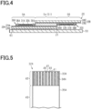
- Fig. 4 is a cross-sectional view taken along the line IV-IV of Fig. 1 .
- the light control sheet 20 includes the light control layer 21, the first electrode sheet 22A, and the second electrode sheet 22B in the inter-terminal region Se located between the first wiring region SA and the second wiring region SB.
- the light control sheet 20 in the inter-terminal region Se and the light control sheet 20 in the main region Sm have the same layer structure.
- Each of the light control layer 21, the first electrode sheet 22A, and the second electrode sheet 22B extends continuously from the main region Sm to the inter-terminal region Se.
- the first electrode sheet 22A extends continuously from the inter-terminal region Se to the first wiring region SA.
- the second electrode sheet 22B extends continuously from the inter-terminal region Se to the second wiring region SB.
- end faces of the light control layer 21, the second transparent electrode layer 23B, and the second transparent support layer 24B are aligned along the thickness direction of the light control sheet 20.
- end faces of the light control layer 21, the first transparent electrode layer 23A, and the first transparent support layer 24A are aligned along the thickness direction of the light control sheet 20.
- the wiring layer 34A of the first wiring member 32A has a conductive patterned end, and is joined to the first conductive adhesive layer 31A at the end.
- the wiring layer 34B of the second wiring member 32B has a conductive patterned end, and is joined to the second conductive adhesive layer 31B at the end.
- Such a conductive pattern is formed, for example, by etching a thin metal film.
- a specific example of this conductive pattern will be described taking the first wiring member 32A as an example.
- dotted regions are used to indicate the position of the pattern of the conductor of the wiring layer 34A.
- the pattern of the conductor may be striped.
- conductive parts 40 where a conductor is located, each have a strip shape extending along the direction of extension of the first wiring member 32A, and the conductive parts 40 are aligned at a fixed interval along a width direction of the first wiring member 32A.
- the conductive pattern has openings 41A, each being a part between two conductive parts 40 adjacent to each other. Each of the openings 41 also has a strip shape extending along the direction of extension of the first wiring member 32A.
- the pattern of the conductor may have a mesh form.
- a conductive part 40 includes a plurality of strips extending along the direction of extension of the first wiring member 32A and a plurality of strips extending along the width direction thereof, with these strips crossing each other to form a mesh pattern.
- Parts of the conductive pattern surrounded by the conductive part 40 are openings 41.
- the openings 41 form dots in the conductive pattern.
- the mesh pattern may be inclined relative to the direction of extension of the first wiring member 32A.
- the conductive part 40 includes a plurality of first strips extending obliquely to the direction of extension of the first wiring member 32A and a plurality of second strips extending along a direction crossing the first strips to form a mesh form.
- the conductive pattern is not limited to the example described above, but may be a pattern in which openings are defined between the conductors.
- the openings 41 may each be sandwiched by the conductive parts 40 along at least one direction. More specifically, the entire periphery of the openings 41 may be surrounded by the conductive parts 40, or be sandwiched by the conductive parts 40 in one direction and not in another direction.
- the insulating resin layer 33A is exposed from the wiring layer 34A. These exposed parts are joined to the first conductive adhesive layer 31A.
- the first conductive adhesive layer 31A is in contact with metal at the conductive part 40 and with a resin at the opening 41.
- the first conductive adhesive layer 31A is thus in partial contact with the resin at the joint part between the first wiring member 32A and the first conductive adhesive layer 31A, thereby strengthening the joint between the first wiring member 32A and the first conductive adhesive layer 31A, compared with the case where the first conductive adhesive layer 31A is in contact only with the metal, that is, the conductive part 40 spreads without any openings 41.
- the ratio of the openings 41 there is no limitation on the ratio of the openings 41, but preferably the openings 41 are evenly arranged.
- the area ratio of the openings 41 to the conductive part 40 is preferably constant per unit area in plan view of a region where the pattern of the conductor is located. Such a configuration prevents unevenness in j oint strength in a j oint part between the first wiring member 32A and the first conductive adhesive layer 31A.
- first wiring member 32A and the first conductive adhesive layer 31A are joined by thermocompression bonding, evenly arranging the openings 41 prevents unevenness in the strength of a force applied to the first conductive adhesive layer 31A during thermocompression bonding. This in turn prevents unevenness in joint strength and in formation of a conductive path in the first conductive adhesive layer 31A.
- the first conductive adhesive layer 31A is composed of an anisotropic conductive adhesive material, a preferable conductive path is formed along the conductive pattern in the first conductive adhesive layer 31A.
- the wiring layer 34A preferably has a patterned part 42 that constitutes the conductive pattern described above and an unpatterned part 43 that spreads without any openings 41.
- the patterned part 42 and the unpatterned part 43 are connected to each other and form a contiguous layer.
- the patterned part 42 and the unpatterned part 43 are electrically connected to each other.
- the unpatterned part 43 is located in a portion of the wiring layer 34A extending from an end thereof where the patterned part 42 is located, that is, in a portion of the first wiring member 32A not connected to the first conductive adhesive layer 31A.
- An end of the first wiring member 32A on a side opposite to that joined to the first conductive adhesive layer 31A is connected to a driver circuit, whereby the first transparent electrode layer 23A and a power supply are electrically connected to each other.
- the driver circuit converts a voltage supplied from the power supply into a driving voltage and applies it to the first transparent electrode layer 23A through the first connection member 30A. It is sufficient that the wiring layer 34A serves as a single wire as a whole. Thus the load required for patterning can be alleviated and a resistance value in the wiring layer 34A can be inhibited from increasing if a part of the wiring layer 34A not connected to the first conductive adhesive layer 31A is unpatterned.
- a portion of the unpatterned part 43 may be located in the part of the first wiring member 32A joined to the first conductive adhesive layer 31A.
- a portion of the patterned part 42 may be located in the part of the first wiring member 32A not connected to the first conductive adhesive layer 31A.
- the wiring layer 34A of the first wiring member 32A and the wiring layer 34B of the second wiring member 32B may have the same or different conductive pattern.
- the light control unit 10 is manufactured, for example, by the following manufacturing method.
- a multilayer sheet having the light control layer 21 and the electrode sheets 22A and 22B is formed.
- the multilayer sheet is then cut or stamped out into a shape corresponding to that of the transparent plate 50 to form a multilayer having the light control layer 21 and the electrode sheets 22A and 22B.
- wiring regions SA and SB are formed and the connection members 30A and 30B are connected thereto.
- the first wiring region SA is formed by removing the second electrode sheet 22B and the light control layer 21 from a part of the multilayer described above.
- the second wiring region SB is formed by removing the first electrode sheet 22A and the light control layer 21 from a part of the multilayer described above.
- the removal of the parts in the electrode sheets 22A and 22B are performed by, for example, cutting off them from the remaining part.
- the removal of the part in the light control layer 21 is performed by, for example, wiping off it.
- the light control 20 is thus formed. With this manufacturing method, arranging the wiring regions SA and SB to include a corner of the light control sheet 20 allows the wiring regions SA and SB to be easily formed.
- connection members 30A and 30B are then arranged and joined on the exposed surface of the transparent electrode layers 23A and 23B, whereby the light control unit 10 is formed.
- a sealant may be formed as necessary on an outer circumference of the light control sheet 20 on the transparent plate 50.
- This manufacturing method aligns end faces of the light control layer 21 and the electrode sheets 22A and 22B in the thickness direction of the light control sheet 20 at an edge of the light control region Si in the light control sheet 20, that is, at an edge that constitutes an outer edge of the light control sheet 20 and at an edge contiguous to the wiring regions SA and SB.
- the above manufacturing method improves the efficiency of manufacturing the light control sheet 20 as compared with a manufacturing method in which for each light control sheet 20, a sealing structure is formed between the electrode sheets 22A and 22B, followed by injecting liquid crystals between the electrode sheets 22A and 22B to form the light control layer 21. Furthermore, since the outer shape of the light control sheet 20 is formed by cutting out or stamping out a multilayer sheet, the manufacturing method facilitates formation of the light control sheet 20 having a shape corresponding to the shape of the transparent plate 50.
- the wiring regions SA and SB are formed by partially removing the light control layer 21 and the electrode sheets 22A and 22B, the light control layer 21 and the electrode sheets 22A and 22B are easily formed as compared with a manufacturing method in which the light control layer 21 and the electrode sheets 22A and 22B are formed that have parts of the wiring regions SA and SB removed. It is also easy to adjust a size and arrangement of the wiring regions SA and SB.
- connection members 30A and 30B are structured such that the wiring layers 34A and 34B of the wiring members 32A and 32B are joined to surfaces of the conductive adhesive layers 31A and 31B, respectively.
- the part where the conductive adhesive layers 31A and 31B are joined to the wiring members 32A and 32B extends in a planar shape.
- Ajoint part between each member constituting the connection members 30A and 30B does not include a dot-like joint structure, such as a lead wire and solder joint. The reliability of connection at the connection members 30A and 30B thus increases.
- connection members 30A and 30B This consequently prevents poor joints at the connection members 30A and 30B even if an external force acts on the connection members 30A and 30B when, for example, the light control unit 10 is mounted on the transparent plate 50 or when the light control unit 10 is moved along with the transparent plate 50, such as when the light control unit 10 is used on a window or the like.
- the wiring layers 34A and 34B have a conductive pattern in a part joined to the adhesive layers 31A and 31B, which enables a more reliable joint at the connection members 30A and 30B, as described above.
- the transparent electrode layers 23A and 23B, to which a signal from the driver circuit is supplied are unpatterned, that is, have no openings, in a joint part with the connection members 30A and 30B.
- the conductive pattern of the wiring layers 34A and 34B does not serve as mutually insulated wiring for supplying separate signals to a plurality of elements.
- the wiring layers 34A and 34B do not need to be patterned in terms of wiring for supplying signals to the transparent electrode layers 23A and 23B.
- forming a conductive pattern on the wiring layers 34A and 34B in the light control unit 10 increases the joint strength between the wiring members 32A and 32B and the conductive adhesive layers 31A and 31B due to the presence of openings between conductors.
- connection members 30A and 30B have sufficient joint reliability in a cool, hot, or humid environment.
- connection members 30A and 30B of the present embodiment are thinner at a part connected to the wiring regions SA and SB than conventional connection members including lead wire and solder. This readily makes it possible to make the first connection member 30A thinner than the total thickness of the light control layer 21 and the second electrode sheet 22B, and also to make the second connection member 30B thinner than the total thickness of the light control layer 21 and the first electrode sheet 22A, as described above. This in turn makes it possible to prevent the connection members 30A and 30B from protruding and suffering an impact upon coming into contact with other members, and also the second electrode sheet 22B from distorting due to a bump of the second wiring region SB in the light control sheet 20.
- the light control unit 10 of the present embodiment achieves the following effects.
- the first wiring member 32A and the second wiring member 32B may be connected to each other outside the light control sheet 20.
- an insulating resin layer 33A of the first wiring member 32A and an insulating resin layer 33B of the second wiring member 32B constitute a single substrate 33, which bifurcates near the light control sheet 20.
- the wiring layer 34A is located on one side of the substrate 33.
- the substrate 33 and the wiring layer 34A constitute the first wiring member 32A.
- the wiring layer 34B is located on the other side of the substrate 33.
- the substrate 33 and the wiring layer 34B constitute the second wiring member 32B. That is, the above embodiment uses a flexible printed circuit board having a metal thin film disposed on both sides of the substrate 33, with the metal film serving as a wiring layer.
- the first modification reduces an area occupied by the connection members 30A and 30B outside the light control sheet 20.
- the first wiring region SA and the second wiring region SB may be disposed along different sides of the light control sheet 20.
- the first connection member 30A and the second connection member 30B may not be aligned along one side of the light control sheet 20.
- the configuration of the second modification allows a higher degree of freedom in arranging the first connection member 30A and the second connection member 30B, and also enables adjustment of the positions of the first connection member 30A and the second connection member 30B depending on the size, location of installation, etc. of the light control sheet 20.
- the light control sheet 20 may have a plurality of first wiring regions SA, to each of which a first connection member 30A may be connected.
- the light control unit 10 may have a plurality of first connection members 30A.
- the plurality of first connection members 30A may be controlled at the same potential, and also be separately connected to the driver circuit.
- the plurality of first connection members 30A may be connected to each other outside the light control sheet 20.
- the plurality of first connection members 30A may constitute a connection member having a single terminal to which a signal is applied from the driver circuit and a plurality of terminals for outputting the signal to the light control sheet 20.
- the configuration described above reduces the load on the driver circuit when controlling the first transparent electrode layer 23A at a predetermined potential.
- the light control sheet 20 may have a plurality of second wiring regions SB
- the light control unit 10 may have a plurality of second connection members 30B, each of which may be connected to a respective one of the second wiring regions SB.
- the plurality of second connection members 30B may be separately connected to the driver circuit and be connected to each other outside the light control sheet 20.
- the configuration described above reduces the load on the driver circuit when controlling the second transparent electrode layer 23B at a predetermined potential.
- the configuration of the third modification is particularly effective when the light control region Si is large.
- the wiring layer 34A may not be patterned in a part of the first wiring member 32A joined to the first conductive adhesive layer 31A.
- the wiring layer 34A may extend without any openings 41, in a part joined to the first conductive adhesive layer 31A.
- the wiring layer 34B may not be patterned in a part of the second wiring member 32B joined to the second conductive adhesive layer 31B.
- the configuration of the fourth, not claimed modification also has a planar joint part between the conductive adhesive layers 31A and 31B and the wiring members 32A and 32B. This improves joint reliability at the connection members 30A and 30B, compared with the case where the connection members 30A and 30B include a dot-like joint structure with solder and lead wire. That is, the effect (1) described above can be obtained.
- the first connection member 30A may not include the first sealing member 36A.
- the second connection member 30B may not include the second sealing member 36B.
- an edge 21a of the light control layer 21 may protrude from an edge of the second electrode sheet 22B at the edge of the light control region Si contiguous to the first wiring region SA, as shown in Fig. 10 .
- an edge of the light control layer 21 may protrude from an edge of the first electrode sheet 22A at the edge of the light control region Si contiguous to the second wiring region SB.
- the protrusion of the light control layer 21 makes it hard for the first transparent electrode layer 23A and the second transparent electrode layer 23B to come into contact with each other even if the light control sheet 20 is crushed at the end of the light control region Si, thereby preventing a short circuit.
- Each end face of the electrode sheets 22A and 22B may not be aligned with a corresponding end face of the light control layer 21 at the edges of the light control region Si, regardless of whether the sealing members 36A and 36B are present.
- Flexible flat cables may be used as the wiring members 32A and 32B.
- a flexible flat cable is structured such that a plurality of conductor strips arranged in parallel are sandwiched by two insulating resin films. At an end of the flexible flat cable, the conductor strips are exposed from the insulating resin films, and these exposed parts are joined to the conductive adhesive layers 31A and 31B.
- the plurality of conductor strips correspond to wiring layers
- the array pattern of the plurality of conductor strips corresponds to a pattern of a conductor
- the insulating resin film corresponds to an insulating resin layer.
- a conductive pattern is formed by etching a metal thin film, which allows a higher degree of freedom in pattern shape and makes it possible to form a fine pattern.
- a flexible flat cable is used as the wiring members 32A and 32B, the wiring members 32A and 32B can be provided at a low cost. Flexible flat cables only allow a limited degree of freedom in pattern shape but still allow adjustment of the ratio of a conductor to an opening through adjustment of the width and array interval of conductor strips, thereby improving the joint strength.
- the wiring members 32A and 32B include at least the wiring layers 34A and 34B and the insulating resin layers 33A and 33B.
- the wiring members 32A and 32B may be, for example, a flexible printed circuit board having a metal thin film on a surface of the insulating resin layers 33A and 33B facing away from the surface joined to the conductive adhesive layers 31A and 31B, respectively.
- the wiring layers 34A and 34B are metal layers and may be composed of a plurality of layers including a plating layer, etc.
- the insulating resin layers 33A and 33B are resin layers and may be composed of a plurality of layers.
- the conductive adhesive layers 31A and 31B are layers that are conductive and adhesive, and may be composed of a plurality of layers.
- the light control sheet 20 may include an additional layer as well as the light control layer 21 and the electrode sheets 22A and 22B.
- additional layers include a layer for protecting the light control layer 21 and the transparent electrode layers 23A and 23B, such as a layer having a UV barrier function; a layer contributing to control optical transparency of the light control sheet 20; and a layer improving characteristics such as strength or heat resistance of the light control sheet 20.
- the light control sheet 20 may include a pair of orientation layers that are located between the light control layer 21 and the electrode sheets 22A and 22B and that sandwich the light control layer 21.
- the orientation layer is a layer that controls orientation of the liquid crystal molecules contained in the light control layer 21. When no driving voltage is applied, the orientation layer orients the liquid crystal molecules in a normal direction thereof. In the configuration including the orientation layer, when no driving voltage is applied across the transparent electrode layers 23A and 23B, the light control region Si is transparent, and when a driving voltage is applied across the transparent electrode layers 23A and 23B, the light control region Si is opaque.
- the light control sheet 20 further includes a layer other than the light control layer 21 and electrode sheets 22A and 22B, in the first wiring region SA, a surface of the first transparent electrode layer 23A is exposed from the other layers and the first connection member 30A is connected to this surface, while in the second wiring region SB, a surface of the second transparent electrode layer 23B is exposed from the other layers and the second connection member 30B is connected to this surface.
- the light control layer 21 may include a dye that has a predetermined color and does not hinder movement of the liquid crystal molecules according to a magnitude of the voltage applied to the light control layer 21. Such a configuration provides a light control sheet 20 having a predetermined color.
- the wiring regions SA and SB may be disposed at a location that does not include a corner of the light control sheet 20. If the light control unit is formed by the manufacturing method of the embodiment described above, the entire region other than the wiring regions SA and SB in the light control sheet 20 serves as the light control region Si.
- the light control sheet 20 may not be rectangular.
- a surface of the transparent plate 50 to which the light control sheet 20 is attached may be flat or curved.
- Using a flexible printed circuit board or a flexible flat cable as the wiring members 32A and 32B keeps the wiring members 32A and 32B highly flexible while improving joint reliability at the connection members 30A and 30B.
- the light control unit 10 thus readily fits with a curved surface, and is therefore suitable for being mounted on a curved surface.
- first electrode sheet 22A or the second electrode sheet 22B may be attached to the transparent plate 50.
- the light control sheet 20 may be sandwiched between two transparent plates 50.
Landscapes
- Physics & Mathematics (AREA)
- Nonlinear Science (AREA)
- Optics & Photonics (AREA)
- Chemical & Material Sciences (AREA)
- Crystallography & Structural Chemistry (AREA)
- General Physics & Mathematics (AREA)
- Engineering & Computer Science (AREA)
- Mathematical Physics (AREA)
- Structural Engineering (AREA)
- Liquid Crystal (AREA)
- Microelectronics & Electronic Packaging (AREA)
- Architecture (AREA)
- Civil Engineering (AREA)
- Health & Medical Sciences (AREA)
- Life Sciences & Earth Sciences (AREA)
- Biodiversity & Conservation Biology (AREA)
- Ecology (AREA)
- Environmental & Geological Engineering (AREA)
- Environmental Sciences (AREA)
- Toxicology (AREA)
- Combinations Of Printed Boards (AREA)
Claims (10)
- Lichtsteuerungseinheit (10), die aufweist:eine Lichtsteuerungsplatte (20), die eine Lichtsteuerungsschicht (21), die eine Flüssigkristallzusammensetzung, eine erste transparente Elektrodenschicht (23A) und eine zweite transparente Elektrodenschicht (23B) aufweist, enthält; undein erstes Verbindungsbauteil (30A), das mit der ersten transparenten Elektrodenschicht verbunden ist und konfiguriert ist, eine elektrische Leistung zu der ersten transparenten Elektrode zu leiten, wobeidie Lichtsteuerungsschicht (21) zwischen der ersten transparenten Elektrodenschicht (23A) und der zweiten transparenten Elektrodenschicht (23B) eingebettet ist;die erste transparente Elektrodenschicht (23A) und die zweite transparente Elektrodenschicht (23B) ungemustert sind;in einer Draufsicht auf die Lichtsteuerungsplatte die erste transparente Elektrodenschicht das erste Verbindungsgebiet (SA), das sich an ein Lichtsteuerungsgebiet (Si) anschließt, enthält, wobei das Lichtsteuerungsgebiet ein Gebiet ist, wo die Lichtsteuerungsschicht lokalisiert ist;das erste Verbindungsbauteil eine erste leitfähige Haftschicht (31A), die mit dem ersten Verbindungsgebiet (SA) und einem ersten Verdrahtungsbauteil (32A), das mit der ersten leitfähigen Haftschicht (31A) verbunden ist, enthält;dadurch gekennzeichnet, dassdas erste Verdrahtungsbauteil eine Verdrahtungsschicht (34A) und eine isolierende Harzschicht (33A), die die Verdrahtungsschicht stützt, enthält, wobei die Verdrahtungsschicht ein leitfähiges gemustertes Ende (42), das leitfähige Teile (40) mit Öffnungen (41) zwischen den leitfähigen Teilen aufweist, aufweist, die Verdrahtungsschicht in Kontakt mit der ersten leitfähigen Haftschicht (31A) an dem gemusterten Ende (42) ist;die isolierende Harzschicht (33A) an den Öffnungen (41) außen liegt, unddie erste leitfähige Haftschicht (31A) in partiellem Kontakt mit der isolierenden Harzschicht (33A) an den Öffnungen (41) ist.
- Lichtsteuerungseinheit nach Anspruch 1, wobei in einer Draufsicht auf ein Gebiet, in dem das leitfähige gemusterte Ende (42) lokalisiert ist, ein Verhältnis zwischen einer Fläche des leitfähigen gemusterten Endes (42) und einer Fläche der Öffnungen (41), die durch das leitfähige gemusterte Ende definiert werden, konstant pro Einheitsfläche ist.
- Lichtsteuerungseinheit nach Anspruch 1 oder 2, wobei das leitfähige gemusterte Ende (42) eine Streifen- oder Maschenform hat.
- Lichtsteuerungseinheit nach einem der Ansprüche 1 bis 3, wobei:die Lichtsteuerungsplatte (20) ferner eine erste transparente Stützschicht (24A), die die erste transparente Elektrodenschicht (23A) stützt, und eine zweite transparente Stützschicht (24B), die die zweite transparente Elektrodenschicht (23B) stützt, enthält; unddas erste Verbindungsbauteil (30A) eine Dicke von weniger als einer gesamten Dicke der Lichtsteuerungsschicht, der zweiten transparenten Elektrodenschicht, und der zweiten transparenten Stützschicht hat.
- Lichtsteuerungseinheit nach einem der Ansprüche 1 bis 4, wobei:die zweite transparente Elektrodenschicht (23B) das zweite Verbindungsgebiet (SB), das sich an das Lichtsteuerungsgebiet (Si) in einer Draufsicht auf die Lichtsteuerungsplatte (20) anschließt, enthält;das zweite Verbindungsbauteil (30B) eine zweite leitfähige Haftschicht (31B), die mit dem zweiten Verbindungsgebiet (SB) verbunden ist, und ein zweites Verdrahtungsbauteil (32B), das mit der zweiten leitfähigen Haftschicht (31B) verbunden ist, enthält; undin einer Draufsicht auf die Lichtsteuerungsplatte (20), das erste Verbindungsgebiet (SA) und das zweite Verbindungsgebiet (SB) entlang einer Seite der Lichtsteuerungsplatte ausgerichtet sind, wobei ein Teil des Lichtsteuerungsgebiets (Se) zwischen dem ersten Verbindungsgebiet und dem zweiten Verbindungsgebiet lokalisiert ist.
- Lichtsteuerungseinheit nach Anspruch 5, wobei:das erste Verbindungsbauteil (30A) und das zweite Verbindungsbauteil (30B) sich zu einer Außenseite der Lichtsteuerungsplatte (20) in einer Draufsicht auf die Lichtsteuerungsplatte erstrecken; unddas erste Verdrahtungsbauteil (32A) und das zweite Verdrahtungsbauteil (32B) außerhalb der Lichtsteuerungsplatte voneinander getrennt sind.
- Lichtsteuerungseinheit nach Anspruch 5, wobei:das erste Verbindungsbauteil und das zweite Verbindungsbauteil sich außerhalb der Lichtsteuerungsplatte in einer Draufsicht auf die Lichtsteuerungsplatte erstrecken; unddas erste Verdrahtungsbauteil und das zweite Verdrahtungsbauteil miteinander außerhalb der Lichtsteuerungsplatte verbunden sind.
- Lichtsteuerungseinheit nach einem der Ansprüche 1 bis 4, wobei:die zweite transparente Elektrodenschicht (23B) das zweite Verbindungsgebiet (SB), das sich an das Lichtsteuerungsgebiet (Si) in einer Draufsicht auf die Lichtsteuerungsplatte (20) anschließt, enthält;das zweite Verbindungsbauteil (30B) eine zweite leitfähige Haftschicht (31B), die mit dem zweiten Verbindungsgebiet und einem zweiten Verdrahtungsbauteil (32B), das mit der zweiten Haftschicht verbunden ist, verbunden ist, enthält; unddas erste Verbindungsgebiet (SA) und das zweite Verbindungsgebiet (SB) entlang unterschiedlicher Seiten der Lichtsteuerungsplatte in einer Draufsicht auf die Lichtsteuerungsplatte angeordnet sind.
- Lichtsteuerungseinheit nach einem der Ansprüche 1 bis 4, wobei:die erste transparente Elektrodenschicht eine Vielzahl von ersten Verbindungsgebieten enthält; unddie Lichtsteuerungseinheit eine Vielzahl von ersten Verbindungsbauteilen enthält,wobei jedes von ihnen mit einer jeweiligen der Vielzahl von ersten Verbindungsgebieten verbunden ist.
- Lichtsteuerungseinheit nach einem der Ansprüche 1 bis 9, wobei:das erste Verdrahtungsbauteil (32A) eine flexible Platine ist;die erste leitfähige Haftschicht (31A) aus einer anisotropen leitfähigen Schicht, einer anisotropen leitfähigen Paste, einer isotropen leitfähigen Schicht, oder einer isotropen leitfähigen Paste zusammengesetzt ist.
Applications Claiming Priority (2)
| Application Number | Priority Date | Filing Date | Title |
|---|---|---|---|
| JP2018073242 | 2018-04-05 | ||
| PCT/JP2019/014972 WO2019194278A1 (ja) | 2018-04-05 | 2019-04-04 | 調光ユニット |
Publications (3)
| Publication Number | Publication Date |
|---|---|
| EP3779583A1 EP3779583A1 (de) | 2021-02-17 |
| EP3779583A4 EP3779583A4 (de) | 2021-06-02 |
| EP3779583B1 true EP3779583B1 (de) | 2023-12-06 |
Family
ID=68100762
Family Applications (1)
| Application Number | Title | Priority Date | Filing Date |
|---|---|---|---|
| EP19782459.2A Active EP3779583B1 (de) | 2018-04-05 | 2019-04-04 | Lichtsteuereinheit |
Country Status (5)
| Country | Link |
|---|---|
| US (1) | US11543719B2 (de) |
| EP (1) | EP3779583B1 (de) |
| JP (2) | JP6939985B2 (de) |
| CN (1) | CN111919165A (de) |
| WO (1) | WO2019194278A1 (de) |
Families Citing this family (12)
| Publication number | Priority date | Publication date | Assignee | Title |
|---|---|---|---|---|
| CN111856830A (zh) * | 2019-09-29 | 2020-10-30 | 法国圣戈班玻璃公司 | 具有分区段调控功能的玻璃以及玻璃分区段调控系统 |
| JP7415638B2 (ja) * | 2020-02-13 | 2024-01-17 | Toppanホールディングス株式会社 | 給電機構および調光体 |
| JP7120291B2 (ja) * | 2020-11-17 | 2022-08-17 | 凸版印刷株式会社 | 調光シート及び調光シートの製造方法 |
| JP7615685B2 (ja) * | 2021-01-06 | 2025-01-17 | Toppanホールディングス株式会社 | 給電部材および給電部材付き調光フィルム |
| JP7585860B2 (ja) * | 2021-02-22 | 2024-11-19 | Toppanホールディングス株式会社 | 調光フィルム及び調光フィルム製造方法 |
| JP7732254B2 (ja) * | 2021-07-14 | 2025-09-02 | Toppanホールディングス株式会社 | 可撓性配線基板、および調光ユニット |
| JP7743768B2 (ja) * | 2021-11-10 | 2025-09-25 | Toppanホールディングス株式会社 | 調光シート |
| JP7743767B2 (ja) * | 2021-11-10 | 2025-09-25 | Toppanホールディングス株式会社 | 調光シート |
| JP7256485B1 (ja) * | 2022-04-13 | 2023-04-12 | 凸版印刷株式会社 | 調光シートの梱包体 |
| EP4531501A4 (de) * | 2022-05-23 | 2026-02-25 | Toppan Holdings Inc | Flexible leiterplatteneinheit und dimmereinheit |
| JP7480219B2 (ja) * | 2022-05-23 | 2024-05-09 | Toppanホールディングス株式会社 | 可撓性配線基板ユニット、及び調光ユニット |
| CN116945717A (zh) * | 2023-07-26 | 2023-10-27 | 览锐光电(镇江)有限公司 | 一种夹层玻璃的制备方法 |
Citations (1)
| Publication number | Priority date | Publication date | Assignee | Title |
|---|---|---|---|---|
| US20110100709A1 (en) * | 2009-10-30 | 2011-05-05 | Dongyan Wang | Spd films and light valve laminates with improved bus-bar connections |
Family Cites Families (27)
| Publication number | Priority date | Publication date | Assignee | Title |
|---|---|---|---|---|
| JPS60140791A (ja) * | 1983-12-27 | 1985-07-25 | ソニ−ケミカル株式会社 | 配線基板 |
| JPH081496B2 (ja) * | 1984-08-22 | 1996-01-10 | シャープ株式会社 | 平面型表示パネルの電極端子取出し構造 |
| JPS6394700A (ja) * | 1986-10-09 | 1988-04-25 | 日東電工株式会社 | 導電性接着テ−プ |
| JP2724471B2 (ja) * | 1988-09-16 | 1998-03-09 | タキロン株式会社 | 調光材及びその製造方法 |
| US5180888A (en) * | 1989-08-10 | 1993-01-19 | Casio Computer Co., Ltd. | Conductive bonding agent and a conductive connecting method |
| JP2847831B2 (ja) * | 1989-12-13 | 1999-01-20 | 富士通株式会社 | フラットディスプレイパルネルの電極端子部接続構造及び電極端子部接続方法 |
| JPH0468317A (ja) * | 1990-07-09 | 1992-03-04 | Semiconductor Energy Lab Co Ltd | 高密着型電極 |
| JP2548484B2 (ja) * | 1992-04-21 | 1996-10-30 | 松下電器産業株式会社 | 液晶表示装置およびその製造方法 |
| WO1995004387A1 (en) * | 1993-07-27 | 1995-02-09 | Citizen Watch Co., Ltd. | An electrical connecting structure and a method for electrically connecting terminals to each other |
| JP2000250060A (ja) * | 1999-02-26 | 2000-09-14 | Toshiba Corp | 液晶表示装置 |
| JP3792554B2 (ja) * | 2001-03-26 | 2006-07-05 | シャープ株式会社 | 表示モジュール及びフレキシブル配線板の接続方法 |
| JP2005107169A (ja) * | 2003-09-30 | 2005-04-21 | Petroleum Energy Center | 熱線遮断素子のリード線取り出し方法 |
| KR101049252B1 (ko) * | 2004-08-23 | 2011-07-13 | 삼성전자주식회사 | 테이프 배선 기판, 그 테이프 배선 기판을 포함하는반도체 칩 패키지 및 그 반도체 칩 패키지를 포함하는액정 표시 장치 |
| JP4387931B2 (ja) | 2004-12-06 | 2009-12-24 | 九州ナノテック光学株式会社 | ポリマーネットワーク型液晶表示装置、及び、その製造方法 |
| JP4579074B2 (ja) * | 2005-07-15 | 2010-11-10 | 三菱電機株式会社 | フレキシブル回路基板及びこれを用いた表示装置 |
| JP4480646B2 (ja) * | 2005-08-25 | 2010-06-16 | 日本電気株式会社 | 光学素子、光源及び表示装置 |
| KR20080031091A (ko) * | 2006-10-03 | 2008-04-08 | 삼성전자주식회사 | 표시장치 및 이의 제조 방법 |
| FR2965641B1 (fr) | 2010-10-04 | 2013-10-11 | Saint Gobain | Vitrage multiple a diffusion variable par cristaux liquides, son procede de fabrication |
| JP6019745B2 (ja) * | 2012-05-21 | 2016-11-02 | 日立化成株式会社 | 導電材付き調光フィルム、及び導電材付き調光フィルムの製造方法 |
| JP6456170B2 (ja) * | 2015-02-02 | 2019-01-23 | デクセリアルズ株式会社 | 接続方法、及び接合体 |
| TWI559826B (zh) * | 2015-12-14 | 2016-11-21 | 財團法人工業技術研究院 | 接合結構及可撓式裝置 |
| JP2018036293A (ja) * | 2016-08-29 | 2018-03-08 | 大日本印刷株式会社 | 調光フィルム |
| JP6094915B1 (ja) | 2016-03-28 | 2017-03-15 | 大日本印刷株式会社 | 液晶セル |
| JP6094916B1 (ja) * | 2016-03-28 | 2017-03-15 | 大日本印刷株式会社 | 液晶セル |
| US10816862B2 (en) * | 2016-05-17 | 2020-10-27 | Merck Patent Gmbh | Device for controlling transmission of radiation |
| JP7119305B2 (ja) * | 2016-07-25 | 2022-08-17 | 凸版印刷株式会社 | 調光体 |
| JP6770859B2 (ja) * | 2016-09-16 | 2020-10-21 | 株式会社ジャパンディスプレイ | 表示装置の製造方法 |
-
2019
- 2019-04-04 EP EP19782459.2A patent/EP3779583B1/de active Active
- 2019-04-04 WO PCT/JP2019/014972 patent/WO2019194278A1/ja not_active Ceased
- 2019-04-04 JP JP2020512320A patent/JP6939985B2/ja active Active
- 2019-04-04 CN CN201980022924.2A patent/CN111919165A/zh active Pending
-
2020
- 2020-10-05 US US17/063,074 patent/US11543719B2/en active Active
-
2021
- 2021-09-02 JP JP2021143448A patent/JP7151843B2/ja active Active
Patent Citations (1)
| Publication number | Priority date | Publication date | Assignee | Title |
|---|---|---|---|---|
| US20110100709A1 (en) * | 2009-10-30 | 2011-05-05 | Dongyan Wang | Spd films and light valve laminates with improved bus-bar connections |
Also Published As
| Publication number | Publication date |
|---|---|
| JP6939985B2 (ja) | 2021-09-22 |
| US11543719B2 (en) | 2023-01-03 |
| US20210018809A1 (en) | 2021-01-21 |
| CN111919165A (zh) | 2020-11-10 |
| EP3779583A4 (de) | 2021-06-02 |
| JP7151843B2 (ja) | 2022-10-12 |
| EP3779583A1 (de) | 2021-02-17 |
| WO2019194278A1 (ja) | 2019-10-10 |
| JPWO2019194278A1 (ja) | 2020-12-03 |
| JP2021185436A (ja) | 2021-12-09 |
Similar Documents
| Publication | Publication Date | Title |
|---|---|---|
| EP3779583B1 (de) | Lichtsteuereinheit | |
| JP3025257B1 (ja) | 表示パネル | |
| JP7377412B2 (ja) | 調光装置 | |
| JP7151137B2 (ja) | 調光ユニット | |
| EP0307231A2 (de) | Anzeigevorrichtung | |
| US8334961B2 (en) | Electrooptical display with electrical crossover | |
| JP4014639B2 (ja) | 液晶表示装置及びそれを用いた電子機器 | |
| JP2007193275A (ja) | 液晶表示装置及びその製造方法 | |
| JP6635156B1 (ja) | 調光ユニット、および、調光板 | |
| KR100856151B1 (ko) | 고분자 분산형 액정표시장치의 전극 단자부 제조방법 | |
| JP7206633B2 (ja) | 調光ユニット | |
| JP2008203448A (ja) | 液晶表示装置 | |
| KR20030077966A (ko) | 1개의 구동ic에 의해 구동되는 액정표시장치 | |
| JP2001042353A (ja) | 積層型液晶表示装置及びその製造方法 | |
| JP6669218B2 (ja) | 調光ユニット、および、透明板付調光ユニット | |
| KR20040011353A (ko) | 액정표시장치 | |
| JPH0452732Y2 (de) | ||
| JP7480219B2 (ja) | 可撓性配線基板ユニット、及び調光ユニット | |
| JP3954152B2 (ja) | パネルの基板とフレキシブル配線板の接続構成及びそれを用いた液晶表示装置 | |
| JP7239902B2 (ja) | 可撓性配線基板、および調光ユニット | |
| JP4201052B2 (ja) | 液晶表示装置及びそれを用いた電子機器 | |
| WO2025216292A1 (ja) | 調光ユニット、および、調光板 | |
| JP2020177040A (ja) | 調光ユニット | |
| JP2024030338A (ja) | 調光装置 | |
| WO2025216293A1 (ja) | 調光ユニット |
Legal Events
| Date | Code | Title | Description |
|---|---|---|---|
| STAA | Information on the status of an ep patent application or granted ep patent |
Free format text: STATUS: THE INTERNATIONAL PUBLICATION HAS BEEN MADE |
|
| PUAI | Public reference made under article 153(3) epc to a published international application that has entered the european phase |
Free format text: ORIGINAL CODE: 0009012 |
|
| STAA | Information on the status of an ep patent application or granted ep patent |
Free format text: STATUS: REQUEST FOR EXAMINATION WAS MADE |
|
| 17P | Request for examination filed |
Effective date: 20200907 |
|
| AK | Designated contracting states |
Kind code of ref document: A1 Designated state(s): AL AT BE BG CH CY CZ DE DK EE ES FI FR GB GR HR HU IE IS IT LI LT LU LV MC MK MT NL NO PL PT RO RS SE SI SK SM TR |
|
| AX | Request for extension of the european patent |
Extension state: BA ME |
|
| A4 | Supplementary search report drawn up and despatched |
Effective date: 20210430 |
|
| RIC1 | Information provided on ipc code assigned before grant |
Ipc: G02F 1/1345 20060101AFI20210426BHEP Ipc: G02F 1/13 20060101ALI20210426BHEP Ipc: G02F 1/1334 20060101ALI20210426BHEP Ipc: G02F 1/1333 20060101ALI20210426BHEP Ipc: E06B 9/24 20060101ALI20210426BHEP Ipc: H01B 7/00 20060101ALI20210426BHEP Ipc: H01B 7/02 20060101ALI20210426BHEP Ipc: H01B 7/18 20060101ALI20210426BHEP Ipc: H01B 7/24 20060101ALI20210426BHEP Ipc: H01B 9/02 20060101ALI20210426BHEP Ipc: H01R 4/02 20060101ALI20210426BHEP Ipc: H01R 4/04 20060101ALI20210426BHEP Ipc: H05K 1/02 20060101ALI20210426BHEP Ipc: H05K 1/14 20060101ALI20210426BHEP Ipc: H01L 23/00 20060101ALI20210426BHEP Ipc: H01R 12/62 20110101ALI20210426BHEP Ipc: H05K 3/32 20060101ALI20210426BHEP |
|
| DAV | Request for validation of the european patent (deleted) | ||
| DAX | Request for extension of the european patent (deleted) | ||
| GRAP | Despatch of communication of intention to grant a patent |
Free format text: ORIGINAL CODE: EPIDOSNIGR1 |
|
| STAA | Information on the status of an ep patent application or granted ep patent |
Free format text: STATUS: GRANT OF PATENT IS INTENDED |
|
| RIC1 | Information provided on ipc code assigned before grant |
Ipc: H05K 1/18 20060101ALN20230517BHEP Ipc: H05K 3/32 20060101ALI20230517BHEP Ipc: H01R 12/62 20110101ALI20230517BHEP Ipc: H01L 23/00 20060101ALI20230517BHEP Ipc: H05K 1/14 20060101ALI20230517BHEP Ipc: H05K 1/02 20060101ALI20230517BHEP Ipc: H01R 4/04 20060101ALI20230517BHEP Ipc: H01R 4/02 20060101ALI20230517BHEP Ipc: H01B 9/02 20060101ALI20230517BHEP Ipc: H01B 7/24 20060101ALI20230517BHEP Ipc: H01B 7/18 20060101ALI20230517BHEP Ipc: H01B 7/02 20060101ALI20230517BHEP Ipc: H01B 7/00 20060101ALI20230517BHEP Ipc: E06B 9/24 20060101ALI20230517BHEP Ipc: G02F 1/1333 20060101ALI20230517BHEP Ipc: G02F 1/1334 20060101ALI20230517BHEP Ipc: G02F 1/13 20060101ALI20230517BHEP Ipc: G02F 1/1345 20060101AFI20230517BHEP |
|
| RIC1 | Information provided on ipc code assigned before grant |
Ipc: H05K 1/18 20060101ALN20230525BHEP Ipc: H05K 3/32 20060101ALI20230525BHEP Ipc: H01R 12/62 20110101ALI20230525BHEP Ipc: H01L 23/00 20060101ALI20230525BHEP Ipc: H05K 1/14 20060101ALI20230525BHEP Ipc: H05K 1/02 20060101ALI20230525BHEP Ipc: H01R 4/04 20060101ALI20230525BHEP Ipc: H01R 4/02 20060101ALI20230525BHEP Ipc: H01B 9/02 20060101ALI20230525BHEP Ipc: H01B 7/24 20060101ALI20230525BHEP Ipc: H01B 7/18 20060101ALI20230525BHEP Ipc: H01B 7/02 20060101ALI20230525BHEP Ipc: H01B 7/00 20060101ALI20230525BHEP Ipc: E06B 9/24 20060101ALI20230525BHEP Ipc: G02F 1/1333 20060101ALI20230525BHEP Ipc: G02F 1/1334 20060101ALI20230525BHEP Ipc: G02F 1/13 20060101ALI20230525BHEP Ipc: G02F 1/1345 20060101AFI20230525BHEP |
|
| RIC1 | Information provided on ipc code assigned before grant |
Ipc: H05K 1/18 20060101ALN20230605BHEP Ipc: H05K 3/32 20060101ALI20230605BHEP Ipc: H01R 12/62 20110101ALI20230605BHEP Ipc: H01L 23/00 20060101ALI20230605BHEP Ipc: H05K 1/14 20060101ALI20230605BHEP Ipc: H05K 1/02 20060101ALI20230605BHEP Ipc: H01R 4/04 20060101ALI20230605BHEP Ipc: H01R 4/02 20060101ALI20230605BHEP Ipc: H01B 9/02 20060101ALI20230605BHEP Ipc: H01B 7/24 20060101ALI20230605BHEP Ipc: H01B 7/18 20060101ALI20230605BHEP Ipc: H01B 7/02 20060101ALI20230605BHEP Ipc: H01B 7/00 20060101ALI20230605BHEP Ipc: E06B 9/24 20060101ALI20230605BHEP Ipc: G02F 1/1333 20060101ALI20230605BHEP Ipc: G02F 1/1334 20060101ALI20230605BHEP Ipc: G02F 1/13 20060101ALI20230605BHEP Ipc: G02F 1/1345 20060101AFI20230605BHEP |
|
| INTG | Intention to grant announced |
Effective date: 20230621 |
|
| GRAS | Grant fee paid |
Free format text: ORIGINAL CODE: EPIDOSNIGR3 |
|
| GRAA | (expected) grant |
Free format text: ORIGINAL CODE: 0009210 |
|
| STAA | Information on the status of an ep patent application or granted ep patent |
Free format text: STATUS: THE PATENT HAS BEEN GRANTED |
|
| AK | Designated contracting states |
Kind code of ref document: B1 Designated state(s): AL AT BE BG CH CY CZ DE DK EE ES FI FR GB GR HR HU IE IS IT LI LT LU LV MC MK MT NL NO PL PT RO RS SE SI SK SM TR |
|
| REG | Reference to a national code |
Ref country code: GB Ref legal event code: FG4D |
|
| REG | Reference to a national code |
Ref country code: CH Ref legal event code: EP |
|
| REG | Reference to a national code |
Ref country code: DE Ref legal event code: R096 Ref document number: 602019042865 Country of ref document: DE |
|
| REG | Reference to a national code |
Ref country code: IE Ref legal event code: FG4D |
|
| REG | Reference to a national code |
Ref country code: LT Ref legal event code: MG9D |
|
| PG25 | Lapsed in a contracting state [announced via postgrant information from national office to epo] |
Ref country code: GR Free format text: LAPSE BECAUSE OF FAILURE TO SUBMIT A TRANSLATION OF THE DESCRIPTION OR TO PAY THE FEE WITHIN THE PRESCRIBED TIME-LIMIT Effective date: 20240307 |
|
| REG | Reference to a national code |
Ref country code: NL Ref legal event code: MP Effective date: 20231206 |
|
| PG25 | Lapsed in a contracting state [announced via postgrant information from national office to epo] |
Ref country code: LT Free format text: LAPSE BECAUSE OF FAILURE TO SUBMIT A TRANSLATION OF THE DESCRIPTION OR TO PAY THE FEE WITHIN THE PRESCRIBED TIME-LIMIT Effective date: 20231206 |
|
| PG25 | Lapsed in a contracting state [announced via postgrant information from national office to epo] |
Ref country code: ES Free format text: LAPSE BECAUSE OF FAILURE TO SUBMIT A TRANSLATION OF THE DESCRIPTION OR TO PAY THE FEE WITHIN THE PRESCRIBED TIME-LIMIT Effective date: 20231206 |
|
| PG25 | Lapsed in a contracting state [announced via postgrant information from national office to epo] |
Ref country code: LT Free format text: LAPSE BECAUSE OF FAILURE TO SUBMIT A TRANSLATION OF THE DESCRIPTION OR TO PAY THE FEE WITHIN THE PRESCRIBED TIME-LIMIT Effective date: 20231206 Ref country code: GR Free format text: LAPSE BECAUSE OF FAILURE TO SUBMIT A TRANSLATION OF THE DESCRIPTION OR TO PAY THE FEE WITHIN THE PRESCRIBED TIME-LIMIT Effective date: 20240307 Ref country code: ES Free format text: LAPSE BECAUSE OF FAILURE TO SUBMIT A TRANSLATION OF THE DESCRIPTION OR TO PAY THE FEE WITHIN THE PRESCRIBED TIME-LIMIT Effective date: 20231206 Ref country code: BG Free format text: LAPSE BECAUSE OF FAILURE TO SUBMIT A TRANSLATION OF THE DESCRIPTION OR TO PAY THE FEE WITHIN THE PRESCRIBED TIME-LIMIT Effective date: 20240306 |
|
| REG | Reference to a national code |
Ref country code: AT Ref legal event code: MK05 Ref document number: 1638960 Country of ref document: AT Kind code of ref document: T Effective date: 20231206 |
|
| PG25 | Lapsed in a contracting state [announced via postgrant information from national office to epo] |
Ref country code: NL Free format text: LAPSE BECAUSE OF FAILURE TO SUBMIT A TRANSLATION OF THE DESCRIPTION OR TO PAY THE FEE WITHIN THE PRESCRIBED TIME-LIMIT Effective date: 20231206 |
|
| PG25 | Lapsed in a contracting state [announced via postgrant information from national office to epo] |
Ref country code: SE Free format text: LAPSE BECAUSE OF FAILURE TO SUBMIT A TRANSLATION OF THE DESCRIPTION OR TO PAY THE FEE WITHIN THE PRESCRIBED TIME-LIMIT Effective date: 20231206 Ref country code: RS Free format text: LAPSE BECAUSE OF FAILURE TO SUBMIT A TRANSLATION OF THE DESCRIPTION OR TO PAY THE FEE WITHIN THE PRESCRIBED TIME-LIMIT Effective date: 20231206 Ref country code: NO Free format text: LAPSE BECAUSE OF FAILURE TO SUBMIT A TRANSLATION OF THE DESCRIPTION OR TO PAY THE FEE WITHIN THE PRESCRIBED TIME-LIMIT Effective date: 20240306 Ref country code: NL Free format text: LAPSE BECAUSE OF FAILURE TO SUBMIT A TRANSLATION OF THE DESCRIPTION OR TO PAY THE FEE WITHIN THE PRESCRIBED TIME-LIMIT Effective date: 20231206 Ref country code: LV Free format text: LAPSE BECAUSE OF FAILURE TO SUBMIT A TRANSLATION OF THE DESCRIPTION OR TO PAY THE FEE WITHIN THE PRESCRIBED TIME-LIMIT Effective date: 20231206 Ref country code: HR Free format text: LAPSE BECAUSE OF FAILURE TO SUBMIT A TRANSLATION OF THE DESCRIPTION OR TO PAY THE FEE WITHIN THE PRESCRIBED TIME-LIMIT Effective date: 20231206 |
|
| PG25 | Lapsed in a contracting state [announced via postgrant information from national office to epo] |
Ref country code: IS Free format text: LAPSE BECAUSE OF FAILURE TO SUBMIT A TRANSLATION OF THE DESCRIPTION OR TO PAY THE FEE WITHIN THE PRESCRIBED TIME-LIMIT Effective date: 20240406 |
|
| PG25 | Lapsed in a contracting state [announced via postgrant information from national office to epo] |
Ref country code: AT Free format text: LAPSE BECAUSE OF FAILURE TO SUBMIT A TRANSLATION OF THE DESCRIPTION OR TO PAY THE FEE WITHIN THE PRESCRIBED TIME-LIMIT Effective date: 20231206 Ref country code: CZ Free format text: LAPSE BECAUSE OF FAILURE TO SUBMIT A TRANSLATION OF THE DESCRIPTION OR TO PAY THE FEE WITHIN THE PRESCRIBED TIME-LIMIT Effective date: 20231206 |
|
| PG25 | Lapsed in a contracting state [announced via postgrant information from national office to epo] |
Ref country code: SK Free format text: LAPSE BECAUSE OF FAILURE TO SUBMIT A TRANSLATION OF THE DESCRIPTION OR TO PAY THE FEE WITHIN THE PRESCRIBED TIME-LIMIT Effective date: 20231206 |
|
| PG25 | Lapsed in a contracting state [announced via postgrant information from national office to epo] |
Ref country code: SM Free format text: LAPSE BECAUSE OF FAILURE TO SUBMIT A TRANSLATION OF THE DESCRIPTION OR TO PAY THE FEE WITHIN THE PRESCRIBED TIME-LIMIT Effective date: 20231206 Ref country code: SK Free format text: LAPSE BECAUSE OF FAILURE TO SUBMIT A TRANSLATION OF THE DESCRIPTION OR TO PAY THE FEE WITHIN THE PRESCRIBED TIME-LIMIT Effective date: 20231206 Ref country code: RO Free format text: LAPSE BECAUSE OF FAILURE TO SUBMIT A TRANSLATION OF THE DESCRIPTION OR TO PAY THE FEE WITHIN THE PRESCRIBED TIME-LIMIT Effective date: 20231206 Ref country code: IS Free format text: LAPSE BECAUSE OF FAILURE TO SUBMIT A TRANSLATION OF THE DESCRIPTION OR TO PAY THE FEE WITHIN THE PRESCRIBED TIME-LIMIT Effective date: 20240406 Ref country code: EE Free format text: LAPSE BECAUSE OF FAILURE TO SUBMIT A TRANSLATION OF THE DESCRIPTION OR TO PAY THE FEE WITHIN THE PRESCRIBED TIME-LIMIT Effective date: 20231206 Ref country code: CZ Free format text: LAPSE BECAUSE OF FAILURE TO SUBMIT A TRANSLATION OF THE DESCRIPTION OR TO PAY THE FEE WITHIN THE PRESCRIBED TIME-LIMIT Effective date: 20231206 Ref country code: AT Free format text: LAPSE BECAUSE OF FAILURE TO SUBMIT A TRANSLATION OF THE DESCRIPTION OR TO PAY THE FEE WITHIN THE PRESCRIBED TIME-LIMIT Effective date: 20231206 |
|
| PG25 | Lapsed in a contracting state [announced via postgrant information from national office to epo] |
Ref country code: PL Free format text: LAPSE BECAUSE OF FAILURE TO SUBMIT A TRANSLATION OF THE DESCRIPTION OR TO PAY THE FEE WITHIN THE PRESCRIBED TIME-LIMIT Effective date: 20231206 Ref country code: PT Free format text: LAPSE BECAUSE OF FAILURE TO SUBMIT A TRANSLATION OF THE DESCRIPTION OR TO PAY THE FEE WITHIN THE PRESCRIBED TIME-LIMIT Effective date: 20240408 |
|
| PG25 | Lapsed in a contracting state [announced via postgrant information from national office to epo] |
Ref country code: PT Free format text: LAPSE BECAUSE OF FAILURE TO SUBMIT A TRANSLATION OF THE DESCRIPTION OR TO PAY THE FEE WITHIN THE PRESCRIBED TIME-LIMIT Effective date: 20240408 Ref country code: PL Free format text: LAPSE BECAUSE OF FAILURE TO SUBMIT A TRANSLATION OF THE DESCRIPTION OR TO PAY THE FEE WITHIN THE PRESCRIBED TIME-LIMIT Effective date: 20231206 |
|
| REG | Reference to a national code |
Ref country code: DE Ref legal event code: R097 Ref document number: 602019042865 Country of ref document: DE |
|
| PG25 | Lapsed in a contracting state [announced via postgrant information from national office to epo] |
Ref country code: DK Free format text: LAPSE BECAUSE OF FAILURE TO SUBMIT A TRANSLATION OF THE DESCRIPTION OR TO PAY THE FEE WITHIN THE PRESCRIBED TIME-LIMIT Effective date: 20231206 |
|
| PLBE | No opposition filed within time limit |
Free format text: ORIGINAL CODE: 0009261 |
|
| STAA | Information on the status of an ep patent application or granted ep patent |
Free format text: STATUS: NO OPPOSITION FILED WITHIN TIME LIMIT |
|
| PG25 | Lapsed in a contracting state [announced via postgrant information from national office to epo] |
Ref country code: SI Free format text: LAPSE BECAUSE OF FAILURE TO SUBMIT A TRANSLATION OF THE DESCRIPTION OR TO PAY THE FEE WITHIN THE PRESCRIBED TIME-LIMIT Effective date: 20231206 |
|
| PG25 | Lapsed in a contracting state [announced via postgrant information from national office to epo] |
Ref country code: SI Free format text: LAPSE BECAUSE OF FAILURE TO SUBMIT A TRANSLATION OF THE DESCRIPTION OR TO PAY THE FEE WITHIN THE PRESCRIBED TIME-LIMIT Effective date: 20231206 Ref country code: DK Free format text: LAPSE BECAUSE OF FAILURE TO SUBMIT A TRANSLATION OF THE DESCRIPTION OR TO PAY THE FEE WITHIN THE PRESCRIBED TIME-LIMIT Effective date: 20231206 |
|
| 26N | No opposition filed |
Effective date: 20240909 |
|
| PG25 | Lapsed in a contracting state [announced via postgrant information from national office to epo] |
Ref country code: MC Free format text: LAPSE BECAUSE OF FAILURE TO SUBMIT A TRANSLATION OF THE DESCRIPTION OR TO PAY THE FEE WITHIN THE PRESCRIBED TIME-LIMIT Effective date: 20231206 |
|
| PG25 | Lapsed in a contracting state [announced via postgrant information from national office to epo] |
Ref country code: MC Free format text: LAPSE BECAUSE OF FAILURE TO SUBMIT A TRANSLATION OF THE DESCRIPTION OR TO PAY THE FEE WITHIN THE PRESCRIBED TIME-LIMIT Effective date: 20231206 |
|
| REG | Reference to a national code |
Ref country code: CH Ref legal event code: PL |
|
| PG25 | Lapsed in a contracting state [announced via postgrant information from national office to epo] |
Ref country code: LU Free format text: LAPSE BECAUSE OF NON-PAYMENT OF DUE FEES Effective date: 20240404 |
|
| PG25 | Lapsed in a contracting state [announced via postgrant information from national office to epo] |
Ref country code: LU Free format text: LAPSE BECAUSE OF NON-PAYMENT OF DUE FEES Effective date: 20240404 |
|
| PG25 | Lapsed in a contracting state [announced via postgrant information from national office to epo] |
Ref country code: CH Free format text: LAPSE BECAUSE OF NON-PAYMENT OF DUE FEES Effective date: 20240430 |
|
| PG25 | Lapsed in a contracting state [announced via postgrant information from national office to epo] |
Ref country code: IE Free format text: LAPSE BECAUSE OF NON-PAYMENT OF DUE FEES Effective date: 20240404 |
|
| PGFP | Annual fee paid to national office [announced via postgrant information from national office to epo] |
Ref country code: BE Payment date: 20250318 Year of fee payment: 7 |
|
| PGFP | Annual fee paid to national office [announced via postgrant information from national office to epo] |
Ref country code: FR Payment date: 20250310 Year of fee payment: 7 |
|
| PGFP | Annual fee paid to national office [announced via postgrant information from national office to epo] |
Ref country code: GB Payment date: 20250227 Year of fee payment: 7 Ref country code: IT Payment date: 20250320 Year of fee payment: 7 |
|
| PGFP | Annual fee paid to national office [announced via postgrant information from national office to epo] |
Ref country code: DE Payment date: 20250305 Year of fee payment: 7 |
|
| PG25 | Lapsed in a contracting state [announced via postgrant information from national office to epo] |
Ref country code: CY Free format text: LAPSE BECAUSE OF FAILURE TO SUBMIT A TRANSLATION OF THE DESCRIPTION OR TO PAY THE FEE WITHIN THE PRESCRIBED TIME-LIMIT; INVALID AB INITIO Effective date: 20190404 |
|
| PG25 | Lapsed in a contracting state [announced via postgrant information from national office to epo] |
Ref country code: HU Free format text: LAPSE BECAUSE OF FAILURE TO SUBMIT A TRANSLATION OF THE DESCRIPTION OR TO PAY THE FEE WITHIN THE PRESCRIBED TIME-LIMIT; INVALID AB INITIO Effective date: 20190404 |
|
| PG25 | Lapsed in a contracting state [announced via postgrant information from national office to epo] |
Ref country code: FI Free format text: LAPSE BECAUSE OF FAILURE TO SUBMIT A TRANSLATION OF THE DESCRIPTION OR TO PAY THE FEE WITHIN THE PRESCRIBED TIME-LIMIT Effective date: 20231207 |
|
| PG25 | Lapsed in a contracting state [announced via postgrant information from national office to epo] |
Ref country code: TR Free format text: LAPSE BECAUSE OF FAILURE TO SUBMIT A TRANSLATION OF THE DESCRIPTION OR TO PAY THE FEE WITHIN THE PRESCRIBED TIME-LIMIT Effective date: 20231206 |