EP3778570B1 - Stark polarisiertes molekül und daraus hergestellter einzelmolekül-feldeffekttransistor - Google Patents
Stark polarisiertes molekül und daraus hergestellter einzelmolekül-feldeffekttransistor Download PDFInfo
- Publication number
- EP3778570B1 EP3778570B1 EP19780897.5A EP19780897A EP3778570B1 EP 3778570 B1 EP3778570 B1 EP 3778570B1 EP 19780897 A EP19780897 A EP 19780897A EP 3778570 B1 EP3778570 B1 EP 3778570B1
- Authority
- EP
- European Patent Office
- Prior art keywords
- molecule
- compound
- field effect
- graphene
- effect transistor
- Prior art date
- Legal status (The legal status is an assumption and is not a legal conclusion. Google has not performed a legal analysis and makes no representation as to the accuracy of the status listed.)
- Active
Links
Images

Classifications
-
- C—CHEMISTRY; METALLURGY
- C07—ORGANIC CHEMISTRY
- C07D—HETEROCYCLIC COMPOUNDS
- C07D487/00—Heterocyclic compounds containing nitrogen atoms as the only ring hetero atoms in the condensed system, not provided for by groups C07D451/00 - C07D477/00
- C07D487/02—Heterocyclic compounds containing nitrogen atoms as the only ring hetero atoms in the condensed system, not provided for by groups C07D451/00 - C07D477/00 in which the condensed system contains two hetero rings
- C07D487/04—Ortho-condensed systems
-
- C—CHEMISTRY; METALLURGY
- C07—ORGANIC CHEMISTRY
- C07C—ACYCLIC OR CARBOCYCLIC COMPOUNDS
- C07C209/00—Preparation of compounds containing amino groups bound to a carbon skeleton
- C07C209/44—Preparation of compounds containing amino groups bound to a carbon skeleton by reduction of carboxylic acids or esters thereof in presence of ammonia or amines, or by reduction of nitriles, carboxylic acid amides, imines or imino-ethers
- C07C209/52—Preparation of compounds containing amino groups bound to a carbon skeleton by reduction of carboxylic acids or esters thereof in presence of ammonia or amines, or by reduction of nitriles, carboxylic acid amides, imines or imino-ethers by reduction of imines or imino-ethers
-
- C—CHEMISTRY; METALLURGY
- C07—ORGANIC CHEMISTRY
- C07C—ACYCLIC OR CARBOCYCLIC COMPOUNDS
- C07C15/00—Cyclic hydrocarbons containing only six-membered aromatic rings as cyclic parts
- C07C15/20—Polycyclic condensed hydrocarbons
-
- C—CHEMISTRY; METALLURGY
- C07—ORGANIC CHEMISTRY
- C07C—ACYCLIC OR CARBOCYCLIC COMPOUNDS
- C07C211/00—Compounds containing amino groups bound to a carbon skeleton
- C07C211/01—Compounds containing amino groups bound to a carbon skeleton having amino groups bound to acyclic carbon atoms
- C07C211/26—Compounds containing amino groups bound to a carbon skeleton having amino groups bound to acyclic carbon atoms of an unsaturated carbon skeleton containing at least one six-membered aromatic ring
- C07C211/30—Compounds containing amino groups bound to a carbon skeleton having amino groups bound to acyclic carbon atoms of an unsaturated carbon skeleton containing at least one six-membered aromatic ring the six-membered aromatic ring being part of a condensed ring system formed by two rings
-
- C—CHEMISTRY; METALLURGY
- C07—ORGANIC CHEMISTRY
- C07C—ACYCLIC OR CARBOCYCLIC COMPOUNDS
- C07C211/00—Compounds containing amino groups bound to a carbon skeleton
- C07C211/01—Compounds containing amino groups bound to a carbon skeleton having amino groups bound to acyclic carbon atoms
- C07C211/26—Compounds containing amino groups bound to a carbon skeleton having amino groups bound to acyclic carbon atoms of an unsaturated carbon skeleton containing at least one six-membered aromatic ring
- C07C211/31—Compounds containing amino groups bound to a carbon skeleton having amino groups bound to acyclic carbon atoms of an unsaturated carbon skeleton containing at least one six-membered aromatic ring the six-membered aromatic ring being part of a condensed ring system formed by at least three rings
-
- C—CHEMISTRY; METALLURGY
- C07—ORGANIC CHEMISTRY
- C07D—HETEROCYCLIC COMPOUNDS
- C07D209/00—Heterocyclic compounds containing five-membered rings, condensed with other rings, with one nitrogen atom as the only ring hetero atom
- C07D209/02—Heterocyclic compounds containing five-membered rings, condensed with other rings, with one nitrogen atom as the only ring hetero atom condensed with one carbocyclic ring
- C07D209/52—Heterocyclic compounds containing five-membered rings, condensed with other rings, with one nitrogen atom as the only ring hetero atom condensed with one carbocyclic ring condensed with a ring other than six-membered
-
- C—CHEMISTRY; METALLURGY
- C07—ORGANIC CHEMISTRY
- C07D—HETEROCYCLIC COMPOUNDS
- C07D333/00—Heterocyclic compounds containing five-membered rings having one sulfur atom as the only ring hetero atom
- C07D333/50—Heterocyclic compounds containing five-membered rings having one sulfur atom as the only ring hetero atom condensed with carbocyclic rings or ring systems
- C07D333/78—Heterocyclic compounds containing five-membered rings having one sulfur atom as the only ring hetero atom condensed with carbocyclic rings or ring systems condensed with rings other than six-membered or with ring systems containing such rings
-
- C—CHEMISTRY; METALLURGY
- C07—ORGANIC CHEMISTRY
- C07F—ACYCLIC, CARBOCYCLIC OR HETEROCYCLIC COMPOUNDS CONTAINING ELEMENTS OTHER THAN CARBON, HYDROGEN, HALOGEN, OXYGEN, NITROGEN, SULFUR, SELENIUM OR TELLURIUM
- C07F15/00—Compounds containing elements of Groups 8, 9, 10 or 18 of the Periodic Table
- C07F15/0006—Compounds containing elements of Groups 8, 9, 10 or 18 of the Periodic Table compounds of the platinum group
- C07F15/0046—Ruthenium compounds
- C07F15/0053—Ruthenium compounds without a metal-carbon linkage
-
- C—CHEMISTRY; METALLURGY
- C07—ORGANIC CHEMISTRY
- C07F—ACYCLIC, CARBOCYCLIC OR HETEROCYCLIC COMPOUNDS CONTAINING ELEMENTS OTHER THAN CARBON, HYDROGEN, HALOGEN, OXYGEN, NITROGEN, SULFUR, SELENIUM OR TELLURIUM
- C07F15/00—Compounds containing elements of Groups 8, 9, 10 or 18 of the Periodic Table
- C07F15/02—Iron compounds
- C07F15/025—Iron compounds without a metal-carbon linkage
-
- C—CHEMISTRY; METALLURGY
- C07—ORGANIC CHEMISTRY
- C07F—ACYCLIC, CARBOCYCLIC OR HETEROCYCLIC COMPOUNDS CONTAINING ELEMENTS OTHER THAN CARBON, HYDROGEN, HALOGEN, OXYGEN, NITROGEN, SULFUR, SELENIUM OR TELLURIUM
- C07F15/00—Compounds containing elements of Groups 8, 9, 10 or 18 of the Periodic Table
- C07F15/02—Iron compounds
- C07F15/03—Sideramines; The corresponding desferri compounds
-
- C—CHEMISTRY; METALLURGY
- C07—ORGANIC CHEMISTRY
- C07F—ACYCLIC, CARBOCYCLIC OR HETEROCYCLIC COMPOUNDS CONTAINING ELEMENTS OTHER THAN CARBON, HYDROGEN, HALOGEN, OXYGEN, NITROGEN, SULFUR, SELENIUM OR TELLURIUM
- C07F15/00—Compounds containing elements of Groups 8, 9, 10 or 18 of the Periodic Table
- C07F15/06—Cobalt compounds
-
- C—CHEMISTRY; METALLURGY
- C07—ORGANIC CHEMISTRY
- C07F—ACYCLIC, CARBOCYCLIC OR HETEROCYCLIC COMPOUNDS CONTAINING ELEMENTS OTHER THAN CARBON, HYDROGEN, HALOGEN, OXYGEN, NITROGEN, SULFUR, SELENIUM OR TELLURIUM
- C07F3/00—Compounds containing elements of Groups 2 or 12 of the Periodic Table
- C07F3/003—Compounds containing elements of Groups 2 or 12 of the Periodic Table without C-Metal linkages
-
- C—CHEMISTRY; METALLURGY
- C07—ORGANIC CHEMISTRY
- C07F—ACYCLIC, CARBOCYCLIC OR HETEROCYCLIC COMPOUNDS CONTAINING ELEMENTS OTHER THAN CARBON, HYDROGEN, HALOGEN, OXYGEN, NITROGEN, SULFUR, SELENIUM OR TELLURIUM
- C07F3/00—Compounds containing elements of Groups 2 or 12 of the Periodic Table
- C07F3/06—Zinc compounds
-
- H—ELECTRICITY
- H10—SEMICONDUCTOR DEVICES; ELECTRIC SOLID-STATE DEVICES NOT OTHERWISE PROVIDED FOR
- H10K—ORGANIC ELECTRIC SOLID-STATE DEVICES
- H10K10/00—Organic devices specially adapted for rectifying, amplifying, oscillating or switching; Organic capacitors or resistors having potential barriers
- H10K10/701—Organic molecular electronic devices
-
- H—ELECTRICITY
- H10—SEMICONDUCTOR DEVICES; ELECTRIC SOLID-STATE DEVICES NOT OTHERWISE PROVIDED FOR
- H10K—ORGANIC ELECTRIC SOLID-STATE DEVICES
- H10K85/00—Organic materials used in the body or electrodes of devices covered by this subclass
- H10K85/30—Coordination compounds
- H10K85/331—Metal complexes comprising an iron-series metal, e.g. Fe, Co, Ni
-
- H—ELECTRICITY
- H10—SEMICONDUCTOR DEVICES; ELECTRIC SOLID-STATE DEVICES NOT OTHERWISE PROVIDED FOR
- H10K—ORGANIC ELECTRIC SOLID-STATE DEVICES
- H10K85/00—Organic materials used in the body or electrodes of devices covered by this subclass
- H10K85/30—Coordination compounds
- H10K85/341—Transition metal complexes, e.g. Ru(II)polypyridine complexes
- H10K85/344—Transition metal complexes, e.g. Ru(II)polypyridine complexes comprising ruthenium
-
- H—ELECTRICITY
- H10—SEMICONDUCTOR DEVICES; ELECTRIC SOLID-STATE DEVICES NOT OTHERWISE PROVIDED FOR
- H10K—ORGANIC ELECTRIC SOLID-STATE DEVICES
- H10K85/00—Organic materials used in the body or electrodes of devices covered by this subclass
- H10K85/30—Coordination compounds
- H10K85/381—Metal complexes comprising a group IIB metal element, e.g. comprising cadmium, mercury or zinc
-
- H—ELECTRICITY
- H10—SEMICONDUCTOR DEVICES; ELECTRIC SOLID-STATE DEVICES NOT OTHERWISE PROVIDED FOR
- H10K—ORGANIC ELECTRIC SOLID-STATE DEVICES
- H10K85/00—Organic materials used in the body or electrodes of devices covered by this subclass
- H10K85/60—Organic compounds having low molecular weight
- H10K85/615—Polycyclic condensed aromatic hydrocarbons, e.g. anthracene
- H10K85/624—Polycyclic condensed aromatic hydrocarbons, e.g. anthracene containing six or more rings
-
- H—ELECTRICITY
- H10—SEMICONDUCTOR DEVICES; ELECTRIC SOLID-STATE DEVICES NOT OTHERWISE PROVIDED FOR
- H10K—ORGANIC ELECTRIC SOLID-STATE DEVICES
- H10K85/00—Organic materials used in the body or electrodes of devices covered by this subclass
- H10K85/60—Organic compounds having low molecular weight
- H10K85/649—Aromatic compounds comprising a hetero atom
- H10K85/655—Aromatic compounds comprising a hetero atom comprising only sulfur as heteroatom
-
- H—ELECTRICITY
- H10—SEMICONDUCTOR DEVICES; ELECTRIC SOLID-STATE DEVICES NOT OTHERWISE PROVIDED FOR
- H10K—ORGANIC ELECTRIC SOLID-STATE DEVICES
- H10K85/00—Organic materials used in the body or electrodes of devices covered by this subclass
- H10K85/60—Organic compounds having low molecular weight
- H10K85/649—Aromatic compounds comprising a hetero atom
- H10K85/657—Polycyclic condensed heteroaromatic hydrocarbons
- H10K85/6572—Polycyclic condensed heteroaromatic hydrocarbons comprising only nitrogen in the heteroaromatic polycondensed ring system, e.g. phenanthroline or carbazole
-
- H—ELECTRICITY
- H10—SEMICONDUCTOR DEVICES; ELECTRIC SOLID-STATE DEVICES NOT OTHERWISE PROVIDED FOR
- H10K—ORGANIC ELECTRIC SOLID-STATE DEVICES
- H10K10/00—Organic devices specially adapted for rectifying, amplifying, oscillating or switching; Organic capacitors or resistors having potential barriers
- H10K10/40—Organic transistors
- H10K10/46—Field-effect transistors, e.g. organic thin-film transistors [OTFT]
Definitions
- This application relates to the technical field of single molecule electronic devices, in particular to a strongly-polarized molecule and a single molecule field effect transistor prepared therefrom.
- transistors In the current semiconductor industry, the core of electronic circuits is transistors, which are the cornerstone of the contemporary digital revolution. Since the first model of transistors was proposed in 1947, researchers have developed various types of transistors.
- the fundamental principle of transistors is that: , as the capacitance effect of the dielectric layer can change the carrier concentration at the interface between the insulation layer and the semiconductor layer, the current between source electrodes and drain electrodes can be modulated by applying an appropriate voltage to the gate. Therefore, on the one hand, the logic function of the switch can be realized, and on the other hand, since the output power is higher than the input power, the transistor has an amplifier function .
- single molecule field effect transistors have also aroused great interest among researchers.
- the electrostatic potential of a molecule in a single molecule heterojunction can be modulated by applying gate voltage, and thereby energy levels of the molecules are changed, which is different from traditional field-effect transistors. Therefore, on the one hand, the conductive properties of the molecule can be modulated, and on the other hand, certain information related to the vibration mode and excited state of the molecule and vibration-related information can be obtained.
- single molecule field effect transistors are still only at the conceptual stage and have not been implemented in the prior art CN102456702 deals with materials for graphene based transistor devices.
- the examples of the present application aim to provide a strongly-polarized molecule and a single molecule field effect transistor prepared therefrom.
- the specific technical solutions are as follows:
- Ph phenyl
- halogen refers to fluorine, chlorine, bromine or iodine.
- C 1-12 alkyl refers to a linear or branched saturated hydrocarbon group containing 1-12 carbon atoms, including but not limited to methyl, ethyl, n-propyl, isopropyl, n-butyl, isobutyl, 3-ethylheptyl and n-dodecyl.
- the " in the structural formula of a group represents the attachment site of the group to the other parts of the molecule.
- the strongly-polarized molecules represented by the aforementioned general formulae (II) has one of the following structural formulae:
- the inventor found that, without being limited to any theory, when a voltage is applied, especially within the gate modulation voltage of -2 V to +2 V, the aforementioned strongly-polarized molecules are prone to polarization so that the molecular orbital energy level shifts for compatible with gate modulation. Therefore, the gate modulation of the single molecule field effect transistor can be effectively realized.
- the present application also provides a strongly-polarized molecule-graphene molecular heterojunction, wherein the molecular heterojunction includes the aforementioned strongly-polarized molecule bridging between layers of the two-dimensional single-layer graphene via amide covalent bonds.
- the two-dimensional single-layer graphene with a nanogap is a two-dimensional single-layer graphene with an array of nanogaps.
- This application also provides a method for preparing a strongly-polarized molecule-graphene molecular heterojunction, which includes the following steps:
- the "two-dimensional single-layer graphene with a nanogap" can be prepared by the method described in the literature (see Angew. Chem. Int. Ed. 2012, 51, 12228 .).
- the "two-dimensional single-layer graphene with a nanogap” or “two-dimensional single-layer graphene with an array of nanogaps” is also referred to as graphene nanogap electrode or graphene nano-electrode in the prior art.
- the two-dimensional single-layer graphene with a nanogap is taken out of the solution, washed with a large amount of acetone and ultrapure water, and dried in N 2 gas stream.
- the ultrapure water used preferably has a resistivity greater than 18 M ⁇ cm.
- This application also provides a single molecule field effect transistor, which may comprise a substrate, a gate, a dielectric layer, and the strongly-polarized molecule-graphene molecule heterojunction.
- the dielectric layer is located between the gate and the strongly-polarized molecule-graphene molecular heterojunction.
- the two-dimensional single-layer graphene on both sides of the gap in the strongly-polarized molecule-graphene molecule heterojunction can be used as source electrodes and drain electrodes of the single-molecule field effect transistor.
- the material of the gate is one of graphene or metallic aluminum.
- the material of the dielectric layer is one of hafnium oxide, zirconium oxide, titanium oxide and aluminum oxide, or any combinations thereof.
- the present application provides a single molecule field effect transistor, wherein:
- the substrate may also be referred to as a base.
- the substrate may be a silicon wafer having a silicon oxide layer, which is commercially available.
- the gate or the strongly-polarized molecule-graphene molecular heterojunction is located on the silicon oxide layer. The inventor found that when the thickness of the silicon oxide layer is 200-400 nm, and preferably 300 nm, the optical contrast of the graphene is better. Of course, those skilled in the art can also use other substrates to implement the technical solutions of the present application.
- the thickness of the dielectric layer is 3-10 nm, preferably 4-7 nm, and more preferably 5 nm.
- the thickness of the gate since it has no substantial influence on the performance of the transistor itself, it is not specifically limited here in the present application.
- the thickness of the gate can be selected by those skilled in the art according to the actual requirements of size of the transistor itself.
- the thickness of aluminum can be selected from 20 to 30 nm, when the metal aluminum is used as the gate material; the thickness of the single-layer graphene itself is less than 1 nm, when graphene is used as the gate material.
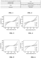
- the present application provides a single-molecule field effect transistor, wherein the gate is located on the substrate, the dielectric layer is located on the gate, and the strongly-polarized molecule-graphene molecule heterojunction is located on the dielectric layer, to form a bottom gate structure, as shown in FIG. 1 ; or the strongly-polarized molecule-graphene molecule heterojunction is located on the substrate, the dielectric layer is located on the strongly-polarized molecule-graphene molecule heterojunction, and the gate is located on the dielectric layer, to form a top gate structure, as shown in FIG. 2 .
- Table 1 Combination of gate and dielectric layer Combination No. 1 2 3 4 5 Gate Graphene Graphene Graphene Aluminum Aluminum Dielectric layer Hafnium oxide Zirconium oxide Titanium oxide Aluminum oxide Aluminum oxide +Hafnium oxide
- the single molecule field effect transistor with a bottom gate structure can be prepared by the following method:
- electron beam evaporation deposition and “atomic layer deposition” herein are both conventional micro-nano processing techniques.
- electron beam evaporation deposition of a metal layer or metal oxide layer with a certain thickness, or atomic layer deposition of a metal layer or metal oxide layer with a certain thickness is very easy to implement for those skilled in the art, which will not be repeated in this application.
- the gate and the dielectric layer when preparing a single molecule field effect transistor with a top gate structure, can also use the 5 combinations in Table 1. Nevertheless, the first three combinations are preferred from the perspective of the simplicity of preparation process.
- a two-dimensional single-layer graphene with a nanogap array is firstly constructed on the substrate. After forming the strongly-polarized molecule-graphene molecule heterojunction by chemical self-assembly method, PMMA (polymethyl methacrylate) is used as a support to transfer the dielectric layer and the gate onto the monomolecular heterojunction.
- PMMA polymethyl methacrylate
- the transfering process of the dielectric layer and the gate may specifically include: firstly, preparing a dielectric layer on a silicon wafer, which may be implemented by using the dielectric layer preparation method in the preparation method of the bottom gate structure, then transferring the graphene grown by chemical vapor deposition on the dielectric layer, further spin-coating PMMA thereon, etching the silicon wafer having hydrofluoric acid, rinsing the dielectric layer/graphene/PMMA film with deionized water and isopropanol three times, and then locatedplacing it on the molecular heterojunction (see ACS Nano 2011, 5, 6916 .).
- support refers to the carrier used to transfer the graphene gate.
- the present application also provides a molecular switch, which includes the aforementioned single molecule field effect transistor.
- the present application also provides a semiconductor chip, which includes the aforementioned single molecule field effect transistor.
- This application provides a strongly-polarized molecule as shown in general formula (II).
- Single molecule field effect transistors are prepared with these molecules for the first time, which is a breakthrough. Since graphene is used as source electrodes and drain electrodes, and the graphene has the matching size with the molecules, which greatly improves the coupling efficiency between the molecules and the gate, and , the efficient gate modulation can be realized cooperating with the strongly-polarized molecule structure.
- the size of the single molecule field effect transistor provided by the present application is within the molecular size range, which strongly promotes the miniaturization of the field effect transistor. Therefore, the semiconductor chip prepared by the single molecule field effect transistor provided by the present application can greatly improve integration. Furthermore, the single molecule field effect transistor provided in the present application has good performance reproducibility, which is more conducive to the application of single molecule field effect transistors.
- the strongly-polarized molecule-graphene molecule heterojunction can be produced in batches
- the single molecule field effect transistor device constructed based on the strongly-polarized molecule-graphene molecule heterojunction provided in this application can be produced in batches.
- the single molecule field effect transistor provided in this application is of epoch-making significance in the technological field of semiconductor.
- the synthetic route is as follows:
- the resultant was circulated 3 times by a freezing and thawing pump circulation method to remove oxygen, and then heated and stirred at 90 °C under the protection of argon for 24 h. After cooling, the reaction mixture was poured into water (50 mL) and extracted with dichloromethane (3 ⁇ 30 mL). After the organic phases were combined and dried over anhydrous sodium sulfate, the solvent was removed under reduced pressure. The crude product was analyzed and purified by silica gel column chromatography to obtain compound B as a purple solid.
- Trifluoroacetic acid (1.0 mL, 0.34 g, 3.73 mmol) was added dropwise to compound B (0.120 g, 0.13 mmol) in dichloromethane (10 mL). After stirring for 2 hours at room temperature, the reaction mixture was added dropwise to saturated aqueous sodium bicarbonate solution (20 mL), and extracted with dichloromethane (50 mL). The organic layer was washed with saturated aqueous sodium bicarbonate solution (30 mL) and saturated sodium chloride solution, and dried over anhydrous sodium sulfate. The solvent was evaporated in vacuo to obtain interested compound 1 as a dark purple solid.
- Graphene was used as the gate electrode, and hafnium oxide with a thickness of 5 nm was used as the dielectric layer to construct a field effect transistor with a bottom gate structure.
- the single-layer graphene grown by chemical vapor deposition was transferred onto a silicon wafer having a oxide layer of 300 nm, as the bottom gate.
- a hafnium oxide layer with a thickness of 5 nm was deposited on the bottom gate by the sol-gel method.
- a two-dimensional single-layer graphene with a nanogap was constructed on the dielectric layer to obtain a molecule device to be assembled.
- a strongly-polarized molecule-graphene molecule heterojunction was constructed on the molecule device to be assembled to obtain a single molecule field effect transistor device.
- the specific process is as follows.
- the compound of formula 1 and the carbodiimide dehydrator-activator 1-ethyl-3-(3-dimethylaminopropyl) carbodiimide hydrochloric acid (EDCI) were dissolved in pyridine.
- the concentrations were 10 -4 mol/L and 3 ⁇ 10 -3 mol/L, respectively.
- the molecule device to be assembled was added into the above solution, and reacted for 48 h in argon atmosphere in dark. After that, the device was taken out of the solution, washed with acetone and ultrapure water three times, respectively, and dried with a nitrogen stream to obtain the compound 1 based single molecule field effect transistor.
- the synthetic route is as follows:
- Compound A was synthesized according to the method of Example 1.
- the resultant was circulated 3 times by a freezing and thawing pump circulation method to remove oxygen, and then heated and stirred at 90 °C under the protection of argon for 24 h. After cooling, the reaction mixture was poured into water (50 mL) and extracted with dichloromethane (3 ⁇ 30 mL). After the organic phases were combined and dried over anhydrous sodium sulfate, the solvent was removed under reduced pressure. The crude product was analyzed and purified by silica gel column chromatography to obtain compound C as a purple solid.
- the locatedreaction was carried out according to the method of Example 1, except that compound B was relocated with compound C (0.120 g, 0.13 mmol), to obtain the interested compound 2 as a dark purple solid.
- a strongly-polarized molecule-graphene molecular heterojunction was constructed to obtain a compound 2 based field effect transistor with bottom gate structure according to the preparation method of transistor in Example 1, in which graphene was used as the gate electrode, hafnium oxide with a thickness of 5 nm was used as the dielectric layer, and compound 2 was used to replace compound 1.
- the synthetic route is as follows:
- Compound A was synthesized according to the method of Example 1.
- the resultant was circulated 3 times by a freezing and thawing pump circulation method to remove oxygen, and then heated and stirred at 90 °C under the protection of argon for 24 h. After cooling, the reaction mixture was poured into water (50 mL) and extracted with dichloromethane (3 ⁇ 30 mL). After the organic phases were and combined and dried over anhydrous sodium sulfate, the solvent was removed under reduced pressure. The crude product was analyzed and purified by silica gel column chromatography to obtain compound D as a purple solid.
- the located reaction was carried out according to the method of Example 1, except that compound B was relocated with compound D (0.127 g, 0.13 mmol), to obtain the interested compound 3 as a dark purple solid.
- a strongly-polarized molecule-graphene molecular heterojunction was constructed to obtain a compound 3 based field effect transistor with bottom gate structure according to the preparation method of transistor in Example 1, in which graphene was used as the gate electrode, hafnium oxide with a thickness of 5 nm was used as the dielectric layer, and compound 3 was used to replace compound 1.
- the synthetic route was as follows.
- reaction solution was poured into dichloromethane (30 mL) and washed with water (2 ⁇ 20 mL) and saturated sodium chloride solution (20 mL), and then dried over anhydrous sodium sulfate. The solvent was removed under reduced pressure. The crude product was analyzed and purified by silica gel column chromatography to obtain compound E as a colorless oily liquid.
- the locatedreaction was carried out according to the method of Example 1, except that compound B was relocated with compound G (0.131g, 0.13mmol), to obtain the interested compound 4 as a dark purple solid.
- a strongly-polarized molecule-graphene molecular heterojunction was constructed to obtain a compound 4 based field effect transistor with bottom gate structure according to the preparation method of transistor in Example 1, in which graphene was used as the gate electrode, hafnium oxide with a thickness of 5 nm was used as the dielectric layer, and compound 4 was used to replace compound 1.
- the synthetic route is as follows:
- Trifluoroacetic acid (1.0 mL, 0.34 g, 3.73 mmol) was added dropwise to compound H (0.173 g, 0.13 mmol) in dichloromethane (10 mL). After stirring for 20 hours at room temperature, the reaction mixture was added dropwise to saturated aqueous sodium bicarbonate solution (20 mL), and extracted with dichloromethane (50 mL). The organic layer was washed with saturated aqueous sodium bicarbonate solution (30 mL) and saturated sodium chloride solution, and dried over anhydrous sodium sulfate. The solvent was evaporated in vacuo to obtain interested compound 5 as a yellow solid.
- a strongly-polarized molecule-graphene molecular heterojunction was constructed to obtain a compound 5 based field effect transistor with bottom gate structure based on compound 5 with reference to the preparation method of transistor in Example 1, in which graphene was used as the gate electrode, hafnium oxide with a thickness of 5 nm was used as the dielectric layer, and compound 5 was used to replace compound 1.
- the synthetic route is as follows:
- a strongly-polarized molecule-graphene molecular heterojunction was constructed to obtain a compound 6 based field effect transistor with bottom gate structure according to the preparation method of transistor in Example 1, in which graphene was used as the gate electrode, hafnium oxide with a thickness of 5 nm was used as the dielectric layer, and compound 6 was used to replace compound 1.
- the synthetic route is as follows:
- a strongly-polarized molecule-graphene molecular heterojunction was constructed to obtain a compound 7 based field effect transistor with bottom gate structure according to the preparation method of transistor in Example 1, in which graphene was used as the gate electrode, hafnium oxide with a thickness of 5 nm was used as the dielectric layer, and compound 7 was used to replace compound 1.
- the synthetic route is as follows:
- reaction solution was poured into dichloromethane (30 mL) and washed with water (2 ⁇ 20 mL) and saturated sodium chloride solution (20 mL) in turn, and then dried over anhydrous sodium sulfate. The solvent was removed under reduced pressure. The crude product was analyzed and purified by silica gel column chromatography to obtain compound N as a white solid.
- Trifluoroacetic acid (1.0 mL, 0.34 g, 3.73 mmol) was added dropwise to compound Q (0.135 g, 0.13 mmol) in dichloromethane (10 mL). After stirring for 20 hours at room temperature, the reaction mixture was added dropwise to saturated aqueous sodium bicarbonate solution (20 mL), and extracted with dichloromethane (50 mL). The organic layer was washed with saturated aqueous sodium bicarbonate solution (30 mL) and saturated sodium chloride solution, and dried over anhydrous sodium sulfate. The solvent was evaporated in vacuo to obtain interested compound 8 as a purple solid.
- a strongly-polarized molecule-graphene molecular heterojunction was constructed to obtain a compound 8 based field effect transistor with bottom gate structure according to the preparation method of transistor in Example 1, in which graphene was used as the gate electrode, hafnium oxide with a thickness of 5 nm was used as the dielectric layer, and compound 8 was used to replace compound 1.
- the synthetic route is as follows:
- a strongly-polarized molecule-graphene molecular heterojunction was constructed to obtain a compound 9 based field effect transistor with bottom gate structure accordingto the preparation method of transistor in Example 1, in which graphene was used as the gate electrode, hafnium oxide with a thickness of 5 nm was used as the dielectric layer, and compound 9 was used to replace compound 1.
- the synthetic route is as follows:
- the locatedreaction was carried out according to the method of Example 8, except that compound Q was relocated with compound S (0.164 g, 0.13 mmol), to obtain the interested compound 10 as a red solid.
- a strongly-polarized molecule-graphene molecular heterojunction was constructed to obtain a compound 10 based field effect transistor with bottom gate structure accordingto the preparation method of transistor in Example 1, in which graphene was used as the gate electrode, hafnium oxide with a thickness of 5 nm was used as the dielectric layer, and compound 10 was used to replace compound 1.
- the synthetic route is as follows:
- reaction was carried out locatedaccording to the method of Example 8, except that compound Q was relocated with compound X (0.283 g, 0.13 mmol), to obtain the interested compound 11 as a red solid.
- a strongly-polarized molecule-graphene molecular heterojunction was constructed to obtain a compound 11 based field effect transistor with bottom gate structure accordingto the preparation method of transistor in Example 1, in which graphene was used as the gate electrode, hafnium oxide with a thickness of 5 nm was used as the dielectric layer, and compound 11 was used to replace compound 1.
- the synthetic route is as follows:
- 1,3-dibromo-5-iodobenzene (1.092 g, 3.02 mmol), 4-(Boc-amino)phenylboronic acid (455 mg, 3.32 mmol), palladium tetrakis(triphenylphosphine) (34.9 mg, 30.3 ⁇ mol), and anhydrous potassium carbonate (3.93 g, 28.5 mmol) were added to a 250 mL Schlenk bottle in sequence, and then 60 mL of tetrahydrofuran and 15 mL of distilled water were injected.
- the resultant was circulated 3 times by a freezing and thawing pump circulation method to remove oxygen, and then heated and stirred at 90 °C under the protection of argon for 24 h. After cooling, the reaction mixture was poured into water (200 mL) and extracted with dichloromethane (3 ⁇ 60 mL). After the organic phases were combined and dried over anhydrous sodium sulfate, the solvent was removed under reduced pressure. The crude product was analyzed and purified by silica gel column chromatography to obtain compound Y.
- reaction was carried out locatedaccording to the method of Example 8, except that compound Q was relocated with compound Z2 (0.282 g, 0.13 mmol), to obtain the interested compound 12 as a purple solid.
- a strongly-polarized molecule-graphene molecular heterojunction was constructed to obtain a compound 12 based field effect transistor with bottom gate structure according to the preparation method of transistor in Example 1, in which graphene was used as the gate electrode, hafnium oxide with a thickness of 5 nm was used as the dielectric layer, and compound 12 was used to replace compound 1.
- the synthetic route is as follows:
- a strongly-polarized molecule-graphene molecular heterojunction was constructed to obtain a compound 13 based field effect transistor with bottom gate structure according to the preparation method of transistor in Example 1, in which graphene was used as the gate electrode, hafnium oxide with a thickness of 5 nm was used as the dielectric layer, and compound 13 was used to replace compound 1.
- the synthetic route is as follows:
- a strongly-polarized molecule-graphene molecular heterojunction was constructed to obtain a compound 14 based field effect transistor with bottom gate structure according to the preparation method of transistor in Example 1, in which graphene was used as the gate electrode, hafnium oxide with a thickness of 5 nm was used as the dielectric layer, and compound 14 was used to replace compound 1.
- Graphene was used as the gate electrode, and zirconium oxide with a thickness of 5 nm was used as the dielectric layer to construct a field effect transistor with a bottom gate structure.
- a bottom gate was formed on the silicon wafer according to the method described in Example 1.
- a zirconium oxide layer with a thickness of 5 nm was deposited on the bottom gate by the electron beam evaporation deposition method.
- Example 1 According to the method described in Example 1, a strongly-polarized molecule-graphene molecule heterojunction was constructed on the dielectric layer to obtain a single molecule field effect transistor device.
- Graphene was used as the gate electrode, and titanium oxide with a thickness of 5 nm was used as the dielectric layer to construct a field effect transistor with a bottom gate structure.
- a bottom gate was formed on the silicon wafer according to the method described in Example 1.
- a titanium oxide layer with a thickness of 5 nm was deposited on the bottom gate by the electron beam evaporation deposition method.
- Example 1 According to the method described in Example 1, a strongly-polarized molecule-graphene molecule heterojunction was constructed on the dielectric layer to obtain a single molecule field effect transistor device.
- Aluminum was used as the gate electrode, and aluminium oxide with a thickness of 5 nm was used as the dielectric layer to construct a field effect transistor with a bottom gate structure.
- an aluminum layer with a thickness of 35 nm was deposited on the silicon wafer by electron beam evaporation deposition method. After that, it was heated at 180 °C for 1 hour to prepare an aluminum oxide layer with a thickness of 5 nm.
- Example 1 According to the method described in Example 1, a strongly-polarized molecule-graphene molecule heterojunction was constructed on the dielectric layer to obtain a single molecule field effect transistor device.
- Aluminum was used as the gate electrode, and aluminium oxide with a thickness of 3 nm and hafnium oxide with a thickness of 2 nm were used as the dielectric layer to construct a field effect transistor with a bottom gate structure.
- an aluminum layer with a thickness of 35 nm was deposited on the silicon wafer by electron beam evaporation deposition method. After that, it was located in the atmosphere for 24 hours, and naturally oxidized to obtain an aluminum oxide layer with a thickness of 3 nm, and then a hafnium oxide layer with a thickness of 2 nm was deposited by atomic layer deposition.
- Example 1 According to the method described in Example 1, a strongly-polarized molecule-graphene molecule heterojunction was constructed on the hafnium oxide layer to obtain a single molecule field effect transistor device.
- Example 19 differs from Example 15 in that the thickness of zirconium oxide was 3 nm.
- Example 20 differs from Example 15 in that the thickness of zirconium oxide was 10 nm.
- Graphene was used as the gate electrode, and hafnium oxide with a thickness of 5 nm was used as the dielectric layer to construct a field effect transistor with a top gate structure.
- hafnium oxide layer with a thickness of 5 nm was prepared by the sol-gel method. After that, the graphene grown by chemical vapor deposition was transferred thereon, on which PMMA was further spin-coated. Finally, the silicon wafer was etched with hydrofluoric acid. The hafnium oxide/graphene/PMMA film was rinsed with deionized water and isopropanol three times, respectively, which was then located on the molecule heterojunction to obtain a single molecule field effect transistor device with a top gate structure based on compound 2.
- Example 22 differs from Example 21 in that: a zirconium oxide layer with a thickness of 5 nm prepared by the electron beam evaporation method was used as the dielectric layer.
- Example 23 differs from Example 21 in that: a titanium oxide layer with a thickness of 5 nm prepared by the atomic layer deposition method was used as the dielectric layer.
- the gate voltage is changed within the range of -2 V to +2 V.
- the source-drain bias voltage (-1 V ⁇ +1 V) was applied with fixing a certain gate voltage.
- I-V characteristic curve of the above-mentioned single molecule field effect transistor modulated by the gate voltage was determined (as shown in FIGs. 3-9 ). It can be seen from FIGs. 3-9 that the single molecule field effect transistor prepared in Examples 1-7 exhibits the conductivity characteristic that it varies with the gate voltage. Specifically, the I-V curves under different gate voltages are significantly different. As the gate voltage changes from negative to positive, the conductivity characteristics significantly change by gradually decreasing. This indicates that the single molecular field effect transistors prepared in Examples 1-7 have efficient gate modulation characteristics. At the same time, it is fully proved that the single molecule field effect transistors provided by the present application have indeed realized the characteristics of industrial transistors and have a wide range of application prospects.
- the single molecule field effect transistors prepared in Examples 8-23 can also fit I-V characteristic curves similar to those of the single molecule field effect transistor prepared in Example 1-7. Therefore, they can achieve the same technical effect of the single molecule field effect transistors prepared in Example 1-7.
Landscapes
- Chemical & Material Sciences (AREA)
- Organic Chemistry (AREA)
- Engineering & Computer Science (AREA)
- Materials Engineering (AREA)
- Physics & Mathematics (AREA)
- Spectroscopy & Molecular Physics (AREA)
- Inorganic Chemistry (AREA)
- Crystallography & Structural Chemistry (AREA)
- Thin Film Transistor (AREA)
- Nitrogen Condensed Heterocyclic Rings (AREA)
- Pyridine Compounds (AREA)
- Organic Low-Molecular-Weight Compounds And Preparation Thereof (AREA)
Claims (12)
- Stark-polarisiertes Molekül, dargestellt durch die allgemeine Formel (II):
 wobei R3 bzw. R4 ausgewählt sind aus Wasserstoff, Halogen, Hydroxyl, Amino, Cyano, Nitro, Carboxyl, C1-12 Alkyl, C1-12 Alkoxy, halogeniertes C1-12 Alkyl, halogeniertes C1-12 Alkoxy, Hydroxyl C1-12 Alkyl, Hydroxyl C1-12 Alkoxy, und C1-12 Alkyl-Amino;x1 und x2 0 sind, bzw. eine positive Zahl, wobei vorzugsweise 0≤x1≤3; 0≤x2≤3.
 - Stark-polarisiertes Molekül gemäss Anspruch 1, aufweisend eine der folgenden Strukturformeln:


- Molekül-Heteroübergang zwischen einem stark-polarisierten Molekül und Graphen, wobei der Molekül-Heteroübergang das stark-polarisierte Molekül gemäss Anspruch 1 oder 2 aufweist, welches via Amid-Kovalentbindungen eine Brücke bildet zwischen Schichten von zweidimensionalem einschichtigem Graphen mit einer Nanolücke; wobei vorzugsweise das zweidimensionale einschichtige Graphen mit einer Nanolücke ein zweidimensionales einschichtiges Graphen mit einem Nanolücken-Array ist.
- Einzelmolekül-Feldeffekttransistor, aufweisend ein Substrat, ein Gate, eine dielektrische Schicht, und den Molekül-Heteroübergang zwischen dem stark-polarisierten Molekül und Graphen gemäss Anspruch 3, wobei die dielektrische Schicht zwischen dem Gate und dem Molekül-Heteroübergang zwischen dem stark-polarisierten Molekül und Graphen angeordnet ist.
- Einzelmolekül-Feldeffekttransistor gemäss Anspruch 4, wobei das Material des Gates ausgewählt ist aus Graphen oder metallischem Aluminium.
- Einzelmolekül-Feldeffekttransistor gemäss Anspruch 4 oder 5, wobei das Material der dielektrischen Schicht ausgewählt ist aus Hafniumoxid, Zirkoniumoxid, Titanoxid, und Aluminiumoxid, oder jeglichen Kombinationen davon.
- Einzelmolekül-Feldeffekttransistor gemäss einem der Ansprüche 4-6, wobei:die dielektrische Schicht eine Hafniumoxidschicht ist und das Gate eine Graphenschicht ist; oderdie dielektrische Schicht eine Zirkoniumoxidschicht ist und das Gate eine Graphenschicht ist; oderdie dielektrische Schicht eine Titanoxidschicht ist und das Gate eine Graphenschicht ist; oderdie dielektrische Schicht eine Aluminiumoxidschicht ist und das Gate eine metallische Aluminiumschicht ist; oderdie dielektrische Schicht eine Kompositschicht ist aus Aluminiumoxid und Hafniumoxid, und das Gate eine metallische Aluminiumschicht ist.
- Einzelmolekül-Feldeffekttransistor gemäss einem der Ansprüche 4-7, wobei das Substrat eine Siliziumscheibe mit einer Siliziumoxidschicht ist, wobei vorzugsweise die Dicke der Siliziumoxidschicht 200-400 nm beträgt und insbesondere bevorzugt 300 nm.
- Einzelmolekül-Feldeffekttransistor gemäss einem der Ansprüche 4-8, wobei die Dicke der dielektrischen Schicht 3-10 nm beträgt, vorzugsweise 4-7 nm, und insbesondere bevorzugt 5 nm.
- Einzelmolekül-Feldeffekttransistor gemäss einem der Ansprüche 4-9, wobei das Gate auf dem Substrat angeordnet ist, die dielektrische Schicht auf dem Gate angeordnet ist und der Molekül-Heteroübergang zwischen dem stark-polarisierten Molekül und Graphen auf der dielektrischen Schicht angeordnet ist; oder
wobei der Molekül-Heteroübergang zwischen dem stark-polarisierten Molekül und Graphen auf dem Substrat angeordnet ist, die dielektrische Schicht auf dem Molekül-Heteroübergang zwischen dem stark-polarisierten Molekül und Graphen angeordnet ist, und das Gate auf der dielektrischen Schicht angeordnet ist. - Molekül-Schalter, aufweisend den Einzelmolekül-Feldeffekttransistor gemäss einem der Ansprüche 4-10.
- Halbleiterchip, aufweisend den Einzelmolekül-Feldeffekttransistor gemäss einem der Ansprüche 4-10.
Applications Claiming Priority (2)
| Application Number | Priority Date | Filing Date | Title |
|---|---|---|---|
| CN201810283361.XA CN110343110B (zh) | 2018-04-02 | 2018-04-02 | 强极化分子及应用其制备的单分子场效应晶体管 |
| PCT/CN2019/080347 WO2019192395A1 (zh) | 2018-04-02 | 2019-03-29 | 强极化分子及应用其制备的单分子场效应晶体管 |
Publications (3)
| Publication Number | Publication Date |
|---|---|
| EP3778570A1 EP3778570A1 (de) | 2021-02-17 |
| EP3778570A4 EP3778570A4 (de) | 2021-09-15 |
| EP3778570B1 true EP3778570B1 (de) | 2023-10-04 |
Family
ID=68100050
Family Applications (1)
| Application Number | Title | Priority Date | Filing Date |
|---|---|---|---|
| EP19780897.5A Active EP3778570B1 (de) | 2018-04-02 | 2019-03-29 | Stark polarisiertes molekül und daraus hergestellter einzelmolekül-feldeffekttransistor |
Country Status (6)
| Country | Link |
|---|---|
| US (1) | US12173016B2 (de) |
| EP (1) | EP3778570B1 (de) |
| JP (1) | JP7083981B2 (de) |
| KR (1) | KR102507357B1 (de) |
| CN (2) | CN110343110B (de) |
| WO (1) | WO2019192395A1 (de) |
Families Citing this family (13)
| Publication number | Priority date | Publication date | Assignee | Title |
|---|---|---|---|---|
| CN111420708B (zh) * | 2020-04-30 | 2021-08-20 | 林贤贵 | 一种石墨烯共价接枝的氨基苯三联吡啶-铁配合物芬顿催化剂及其制备方法 |
| CN112582541B (zh) * | 2020-12-06 | 2022-07-29 | 南开大学 | 一种基于二维叠层异质结构的垂直单分子膜场效应晶体管及其制备方法 |
| CN112582540B (zh) * | 2020-12-06 | 2022-09-30 | 南开大学 | 具有量子干涉效应的化合物及包含其的垂直单分子场效应晶体管集成器件的制备方法 |
| CN112582542B (zh) * | 2020-12-06 | 2022-09-30 | 南开大学 | 一种基于二维范德华异质结构的单分子场效应晶体管及其制备方法 |
| US11390160B2 (en) * | 2020-12-09 | 2022-07-19 | Ford Global Technologies, Llc | Wheel disconnect clutch |
| CN114031753B (zh) * | 2020-12-31 | 2023-11-03 | 广东聚华印刷显示技术有限公司 | 有机聚合物及其应用 |
| CN112898582B (zh) * | 2021-01-19 | 2022-12-20 | 南开大学 | 一种基于超分子的单分子场效应晶体管及其制备方法 |
| CN114213258B (zh) * | 2021-12-13 | 2024-06-18 | 北京未名元上分子技术有限公司 | 一种平面共轭分子化合物及包含其的单分子场效应晶体管 |
| CN114230378B (zh) * | 2021-12-27 | 2022-11-15 | 复旦大学 | 一种氧化还原驱动的超组装智能门控系统的制备方法 |
| CN114292201B (zh) * | 2021-12-27 | 2024-05-28 | 北京未名元上分子技术有限公司 | 一种具有量子干涉效应的化合物及包含其的单分子场效应晶体管 |
| CN117285549A (zh) * | 2023-10-20 | 2023-12-26 | 南开大学 | 金属纳米团簇化合物和石墨烯单分子场效应晶体管 |
| CN118234253B (zh) * | 2024-05-24 | 2024-09-10 | 南开大学 | 一种基于双栅调控的单分子场效应晶体管及其制备方法 |
| CN119947557B (zh) * | 2025-04-07 | 2025-06-03 | 南开大学 | 基于飞秒双光子吸收的双色光源单分子器件及其制备方法 |
Family Cites Families (9)
| Publication number | Priority date | Publication date | Assignee | Title |
|---|---|---|---|---|
| CN102456702B (zh) * | 2010-10-14 | 2014-03-19 | 北京大学 | 一种基于石墨烯电极的功能化分子电子器件及其制备方法与应用 |
| CN102775273B (zh) * | 2012-07-05 | 2014-09-10 | 北京大学 | 一种分叉烷基链及其制备和在有机共轭分子中的应用 |
| CN104177366A (zh) | 2013-05-27 | 2014-12-03 | 海洋王照明科技股份有限公司 | 含吡咯并吡咯烷酮单元的有机半导体材料及其制备方法和太阳能电池器件 |
| JP6158013B2 (ja) * | 2013-09-24 | 2017-07-05 | 株式会社東芝 | 有機分子メモリ |
| KR102254014B1 (ko) * | 2013-12-19 | 2021-05-20 | 메르크 파텐트 게엠베하 | 염료 화합물 |
| KR101608579B1 (ko) * | 2014-04-22 | 2016-04-04 | 한국생산기술연구원 | 전자 수송 재료 및 이를 이용한 유기 전기 발광 소자 |
| CN107098814A (zh) | 2015-03-04 | 2017-08-29 | 湖南工业大学 | 具有高平面性的含萘和酰胺结构功能二胺单体及其合成方法和应用 |
| KR101703118B1 (ko) | 2015-10-14 | 2017-02-07 | 한국생산기술연구원 | 전자 수송 재료 및 이를 이용한 유기 전기 발광 소자 |
| CN107011317B (zh) * | 2016-05-24 | 2020-03-20 | 北京大学 | 光致异构化合物及包含其的器件 |
-
2018
- 2018-04-02 CN CN201810283361.XA patent/CN110343110B/zh active Active
- 2018-04-02 CN CN202011405289.7A patent/CN112538085B/zh active Active
-
2019
- 2019-03-29 WO PCT/CN2019/080347 patent/WO2019192395A1/zh not_active Ceased
- 2019-03-29 EP EP19780897.5A patent/EP3778570B1/de active Active
- 2019-03-29 US US17/042,800 patent/US12173016B2/en active Active
- 2019-03-29 KR KR1020207031057A patent/KR102507357B1/ko active Active
- 2019-03-29 JP JP2020550619A patent/JP7083981B2/ja active Active
Also Published As
| Publication number | Publication date |
|---|---|
| CN112538085A (zh) | 2021-03-23 |
| JP7083981B2 (ja) | 2022-06-14 |
| CN110343110B (zh) | 2021-05-28 |
| EP3778570A4 (de) | 2021-09-15 |
| WO2019192395A1 (zh) | 2019-10-10 |
| EP3778570A1 (de) | 2021-02-17 |
| CN110343110A (zh) | 2019-10-18 |
| JP2021516868A (ja) | 2021-07-08 |
| US20210024560A1 (en) | 2021-01-28 |
| CN112538085B (zh) | 2022-04-05 |
| KR20200138784A (ko) | 2020-12-10 |
| KR102507357B1 (ko) | 2023-03-08 |
| US12173016B2 (en) | 2024-12-24 |
Similar Documents
| Publication | Publication Date | Title |
|---|---|---|
| EP3778570B1 (de) | Stark polarisiertes molekül und daraus hergestellter einzelmolekül-feldeffekttransistor | |
| Rudebusch et al. | Quinoidal diindenothienoacenes: synthesis and properties of new functional organic materials | |
| EP2368892A1 (de) | Neuartige verbindung, verfahren zur herstellung der verbindung, organisches halbleitermaterial und organisches halbleiterbauelement | |
| Yu et al. | Designed synthesis and supramolecular architectures of furan-substituted perylene diimide | |
| CN106366084A (zh) | 一种三重对称三氮杂纳米石墨烯分子及其制备方法 | |
| CN107628924A (zh) | 一种蒽类衍生物及其制备方法与应用 | |
| Fang et al. | Chalcogen bridged pyrene derivatives: Synthesis, crystal− packing structures and field effect transistors properties | |
| Alam et al. | Comparing the impact of trifluoromethyl versus methoxy group on optoelectronic properties of novel 9, 9′-spirobifluorene-based hole transporting materials: Synthesis and computational studies | |
| Rajwar et al. | Synthesis and 2D self-assembly at the liquid-solid interface of end-substituted star-shaped oligophenylenes | |
| Wang et al. | Facile and versatile access to substituted hexabenzoovalene derivatives: characterization and optoelectronic properties | |
| Werner et al. | Reductive O-triflylation of naphthalene diimide: access to alkyne-and amine-functionalized 2, 7-diazapyrenes | |
| CN115626911B (zh) | 反式二噻吩乙烯类衍生物及其制备方法和应用 | |
| Nakano et al. | Synthesis and intramolecular magnetic interaction of triphenylamine derivatives with nitronyl nitroxide radicals | |
| CN108997404A (zh) | 一种光敏剂、制备方法及其应用 | |
| Hallani et al. | The effect of regioisomerism on the crystal packing and device performance of desymmetrized anthradithiophenes | |
| CN107033152A (zh) | 一种多聚酞菁化合物、有机场效应晶体管及其制备方法 | |
| JP4612443B2 (ja) | 機能性有機薄膜、有機薄膜トランジスタ及びそれらの製造方法 | |
| CN101353352A (zh) | 并六噻吩及其衍生物和它们的制备方法与应用 | |
| CN119947557B (zh) | 基于飞秒双光子吸收的双色光源单分子器件及其制备方法 | |
| Carcel et al. | Synthesis and redox properties of several new oligoTTF containing functional spacer | |
| US9773988B2 (en) | Diindenoanthracene and diindenopentacene | |
| CN113735876B (zh) | 一种不对称结构的苯并噻吩并噻吩并苯(btbt)衍生物及其制备方法与应用 | |
| CN102977084A (zh) | 噻吩吡咯醌型结构n-型半导体材料的合成及包含该材料的半导体设备 | |
| JP2003300982A (ja) | 分子集合体、及び分子集合体の製造方法 | |
| CN102007112A (zh) | 有机半导体化合物、半导体器件、太阳能电池及有机半导体化合物的制造方法 |
Legal Events
| Date | Code | Title | Description |
|---|---|---|---|
| STAA | Information on the status of an ep patent application or granted ep patent |
Free format text: STATUS: THE INTERNATIONAL PUBLICATION HAS BEEN MADE |
|
| PUAI | Public reference made under article 153(3) epc to a published international application that has entered the european phase |
Free format text: ORIGINAL CODE: 0009012 |
|
| STAA | Information on the status of an ep patent application or granted ep patent |
Free format text: STATUS: REQUEST FOR EXAMINATION WAS MADE |
|
| 17P | Request for examination filed |
Effective date: 20201001 |
|
| AK | Designated contracting states |
Kind code of ref document: A1 Designated state(s): AL AT BE BG CH CY CZ DE DK EE ES FI FR GB GR HR HU IE IS IT LI LT LU LV MC MK MT NL NO PL PT RO RS SE SI SK SM TR |
|
| AX | Request for extension of the european patent |
Extension state: BA ME |
|
| RIC1 | Information provided on ipc code assigned before grant |
Ipc: C07D 209/52 20060101AFI20210508BHEP Ipc: C07C 15/20 20060101ALI20210508BHEP Ipc: C07D 333/78 20060101ALI20210508BHEP Ipc: C07F 15/00 20060101ALI20210508BHEP Ipc: H01L 51/05 20060101ALI20210508BHEP Ipc: C07C 209/52 20060101ALI20210508BHEP Ipc: C07F 15/06 20060101ALI20210508BHEP |
|
| DAV | Request for validation of the european patent (deleted) | ||
| DAX | Request for extension of the european patent (deleted) | ||
| A4 | Supplementary search report drawn up and despatched |
Effective date: 20210817 |
|
| RIC1 | Information provided on ipc code assigned before grant |
Ipc: C07F 15/06 20060101ALI20210811BHEP Ipc: C07C 209/52 20060101ALI20210811BHEP Ipc: H01L 51/05 20060101ALI20210811BHEP Ipc: C07F 15/00 20060101ALI20210811BHEP Ipc: C07D 333/78 20060101ALI20210811BHEP Ipc: C07C 15/20 20060101ALI20210811BHEP Ipc: C07D 209/52 20060101AFI20210811BHEP |
|
| GRAP | Despatch of communication of intention to grant a patent |
Free format text: ORIGINAL CODE: EPIDOSNIGR1 |
|
| STAA | Information on the status of an ep patent application or granted ep patent |
Free format text: STATUS: GRANT OF PATENT IS INTENDED |
|
| RIC1 | Information provided on ipc code assigned before grant |
Ipc: C07C 211/30 20060101ALN20230330BHEP Ipc: C07C 15/20 20060101ALN20230330BHEP Ipc: C07D 333/78 20060101ALN20230330BHEP Ipc: C07C 209/52 20060101ALN20230330BHEP Ipc: C07F 15/03 20060101ALN20230330BHEP Ipc: H10K 10/46 20230101ALN20230330BHEP Ipc: H10K 10/00 20230101ALI20230330BHEP Ipc: C07F 3/06 20060101ALI20230330BHEP Ipc: C07F 15/06 20060101ALI20230330BHEP Ipc: C07D 487/04 20060101ALI20230330BHEP Ipc: C07C 211/31 20060101ALI20230330BHEP Ipc: C07F 15/00 20060101ALI20230330BHEP Ipc: C07C 5/00 20060101ALI20230330BHEP Ipc: C07D 209/52 20060101AFI20230330BHEP |
|
| INTG | Intention to grant announced |
Effective date: 20230502 |
|
| GRAS | Grant fee paid |
Free format text: ORIGINAL CODE: EPIDOSNIGR3 |
|
| GRAA | (expected) grant |
Free format text: ORIGINAL CODE: 0009210 |
|
| STAA | Information on the status of an ep patent application or granted ep patent |
Free format text: STATUS: THE PATENT HAS BEEN GRANTED |
|
| AK | Designated contracting states |
Kind code of ref document: B1 Designated state(s): AL AT BE BG CH CY CZ DE DK EE ES FI FR GB GR HR HU IE IS IT LI LT LU LV MC MK MT NL NO PL PT RO RS SE SI SK SM TR |
|
| REG | Reference to a national code |
Ref country code: GB Ref legal event code: FG4D |
|
| REG | Reference to a national code |
Ref country code: CH Ref legal event code: EP |
|
| REG | Reference to a national code |
Ref country code: DE Ref legal event code: R096 Ref document number: 602019038724 Country of ref document: DE |
|
| REG | Reference to a national code |
Ref country code: IE Ref legal event code: FG4D |
|
| P01 | Opt-out of the competence of the unified patent court (upc) registered |
Effective date: 20231130 |
|
| REG | Reference to a national code |
Ref country code: LT Ref legal event code: MG9D |
|
| REG | Reference to a national code |
Ref country code: NL Ref legal event code: MP Effective date: 20231004 |
|
| REG | Reference to a national code |
Ref country code: AT Ref legal event code: MK05 Ref document number: 1617656 Country of ref document: AT Kind code of ref document: T Effective date: 20231004 |
|
| PG25 | Lapsed in a contracting state [announced via postgrant information from national office to epo] |
Ref country code: NL Free format text: LAPSE BECAUSE OF FAILURE TO SUBMIT A TRANSLATION OF THE DESCRIPTION OR TO PAY THE FEE WITHIN THE PRESCRIBED TIME-LIMIT Effective date: 20231004 |
|
| PG25 | Lapsed in a contracting state [announced via postgrant information from national office to epo] |
Ref country code: GR Free format text: LAPSE BECAUSE OF FAILURE TO SUBMIT A TRANSLATION OF THE DESCRIPTION OR TO PAY THE FEE WITHIN THE PRESCRIBED TIME-LIMIT Effective date: 20240105 |
|
| PG25 | Lapsed in a contracting state [announced via postgrant information from national office to epo] |
Ref country code: IS Free format text: LAPSE BECAUSE OF FAILURE TO SUBMIT A TRANSLATION OF THE DESCRIPTION OR TO PAY THE FEE WITHIN THE PRESCRIBED TIME-LIMIT Effective date: 20240204 |
|
| PG25 | Lapsed in a contracting state [announced via postgrant information from national office to epo] |
Ref country code: LT Free format text: LAPSE BECAUSE OF FAILURE TO SUBMIT A TRANSLATION OF THE DESCRIPTION OR TO PAY THE FEE WITHIN THE PRESCRIBED TIME-LIMIT Effective date: 20231004 |
|
| PG25 | Lapsed in a contracting state [announced via postgrant information from national office to epo] |
Ref country code: AT Free format text: LAPSE BECAUSE OF FAILURE TO SUBMIT A TRANSLATION OF THE DESCRIPTION OR TO PAY THE FEE WITHIN THE PRESCRIBED TIME-LIMIT Effective date: 20231004 |
|
| PG25 | Lapsed in a contracting state [announced via postgrant information from national office to epo] |
Ref country code: ES Free format text: LAPSE BECAUSE OF FAILURE TO SUBMIT A TRANSLATION OF THE DESCRIPTION OR TO PAY THE FEE WITHIN THE PRESCRIBED TIME-LIMIT Effective date: 20231004 |
|
| PG25 | Lapsed in a contracting state [announced via postgrant information from national office to epo] |
Ref country code: LT Free format text: LAPSE BECAUSE OF FAILURE TO SUBMIT A TRANSLATION OF THE DESCRIPTION OR TO PAY THE FEE WITHIN THE PRESCRIBED TIME-LIMIT Effective date: 20231004 Ref country code: IS Free format text: LAPSE BECAUSE OF FAILURE TO SUBMIT A TRANSLATION OF THE DESCRIPTION OR TO PAY THE FEE WITHIN THE PRESCRIBED TIME-LIMIT Effective date: 20240204 Ref country code: GR Free format text: LAPSE BECAUSE OF FAILURE TO SUBMIT A TRANSLATION OF THE DESCRIPTION OR TO PAY THE FEE WITHIN THE PRESCRIBED TIME-LIMIT Effective date: 20240105 Ref country code: ES Free format text: LAPSE BECAUSE OF FAILURE TO SUBMIT A TRANSLATION OF THE DESCRIPTION OR TO PAY THE FEE WITHIN THE PRESCRIBED TIME-LIMIT Effective date: 20231004 Ref country code: BG Free format text: LAPSE BECAUSE OF FAILURE TO SUBMIT A TRANSLATION OF THE DESCRIPTION OR TO PAY THE FEE WITHIN THE PRESCRIBED TIME-LIMIT Effective date: 20240104 Ref country code: AT Free format text: LAPSE BECAUSE OF FAILURE TO SUBMIT A TRANSLATION OF THE DESCRIPTION OR TO PAY THE FEE WITHIN THE PRESCRIBED TIME-LIMIT Effective date: 20231004 Ref country code: PT Free format text: LAPSE BECAUSE OF FAILURE TO SUBMIT A TRANSLATION OF THE DESCRIPTION OR TO PAY THE FEE WITHIN THE PRESCRIBED TIME-LIMIT Effective date: 20240205 |
|
| PG25 | Lapsed in a contracting state [announced via postgrant information from national office to epo] |
Ref country code: SE Free format text: LAPSE BECAUSE OF FAILURE TO SUBMIT A TRANSLATION OF THE DESCRIPTION OR TO PAY THE FEE WITHIN THE PRESCRIBED TIME-LIMIT Effective date: 20231004 Ref country code: RS Free format text: LAPSE BECAUSE OF FAILURE TO SUBMIT A TRANSLATION OF THE DESCRIPTION OR TO PAY THE FEE WITHIN THE PRESCRIBED TIME-LIMIT Effective date: 20231004 Ref country code: PL Free format text: LAPSE BECAUSE OF FAILURE TO SUBMIT A TRANSLATION OF THE DESCRIPTION OR TO PAY THE FEE WITHIN THE PRESCRIBED TIME-LIMIT Effective date: 20231004 Ref country code: NO Free format text: LAPSE BECAUSE OF FAILURE TO SUBMIT A TRANSLATION OF THE DESCRIPTION OR TO PAY THE FEE WITHIN THE PRESCRIBED TIME-LIMIT Effective date: 20240104 Ref country code: LV Free format text: LAPSE BECAUSE OF FAILURE TO SUBMIT A TRANSLATION OF THE DESCRIPTION OR TO PAY THE FEE WITHIN THE PRESCRIBED TIME-LIMIT Effective date: 20231004 Ref country code: HR Free format text: LAPSE BECAUSE OF FAILURE TO SUBMIT A TRANSLATION OF THE DESCRIPTION OR TO PAY THE FEE WITHIN THE PRESCRIBED TIME-LIMIT Effective date: 20231004 |
|
| REG | Reference to a national code |
Ref country code: DE Ref legal event code: R097 Ref document number: 602019038724 Country of ref document: DE |
|
| PG25 | Lapsed in a contracting state [announced via postgrant information from national office to epo] |
Ref country code: DK Free format text: LAPSE BECAUSE OF FAILURE TO SUBMIT A TRANSLATION OF THE DESCRIPTION OR TO PAY THE FEE WITHIN THE PRESCRIBED TIME-LIMIT Effective date: 20231004 |
|
| PG25 | Lapsed in a contracting state [announced via postgrant information from national office to epo] |
Ref country code: CZ Free format text: LAPSE BECAUSE OF FAILURE TO SUBMIT A TRANSLATION OF THE DESCRIPTION OR TO PAY THE FEE WITHIN THE PRESCRIBED TIME-LIMIT Effective date: 20231004 |
|
| PG25 | Lapsed in a contracting state [announced via postgrant information from national office to epo] |
Ref country code: SK Free format text: LAPSE BECAUSE OF FAILURE TO SUBMIT A TRANSLATION OF THE DESCRIPTION OR TO PAY THE FEE WITHIN THE PRESCRIBED TIME-LIMIT Effective date: 20231004 |
|
| PG25 | Lapsed in a contracting state [announced via postgrant information from national office to epo] |
Ref country code: SM Free format text: LAPSE BECAUSE OF FAILURE TO SUBMIT A TRANSLATION OF THE DESCRIPTION OR TO PAY THE FEE WITHIN THE PRESCRIBED TIME-LIMIT Effective date: 20231004 Ref country code: SK Free format text: LAPSE BECAUSE OF FAILURE TO SUBMIT A TRANSLATION OF THE DESCRIPTION OR TO PAY THE FEE WITHIN THE PRESCRIBED TIME-LIMIT Effective date: 20231004 Ref country code: RO Free format text: LAPSE BECAUSE OF FAILURE TO SUBMIT A TRANSLATION OF THE DESCRIPTION OR TO PAY THE FEE WITHIN THE PRESCRIBED TIME-LIMIT Effective date: 20231004 Ref country code: IT Free format text: LAPSE BECAUSE OF FAILURE TO SUBMIT A TRANSLATION OF THE DESCRIPTION OR TO PAY THE FEE WITHIN THE PRESCRIBED TIME-LIMIT Effective date: 20231004 Ref country code: EE Free format text: LAPSE BECAUSE OF FAILURE TO SUBMIT A TRANSLATION OF THE DESCRIPTION OR TO PAY THE FEE WITHIN THE PRESCRIBED TIME-LIMIT Effective date: 20231004 Ref country code: DK Free format text: LAPSE BECAUSE OF FAILURE TO SUBMIT A TRANSLATION OF THE DESCRIPTION OR TO PAY THE FEE WITHIN THE PRESCRIBED TIME-LIMIT Effective date: 20231004 Ref country code: CZ Free format text: LAPSE BECAUSE OF FAILURE TO SUBMIT A TRANSLATION OF THE DESCRIPTION OR TO PAY THE FEE WITHIN THE PRESCRIBED TIME-LIMIT Effective date: 20231004 |
|
| PLBE | No opposition filed within time limit |
Free format text: ORIGINAL CODE: 0009261 |
|
| STAA | Information on the status of an ep patent application or granted ep patent |
Free format text: STATUS: NO OPPOSITION FILED WITHIN TIME LIMIT |
|
| 26N | No opposition filed |
Effective date: 20240705 |
|
| PG25 | Lapsed in a contracting state [announced via postgrant information from national office to epo] |
Ref country code: SI Free format text: LAPSE BECAUSE OF FAILURE TO SUBMIT A TRANSLATION OF THE DESCRIPTION OR TO PAY THE FEE WITHIN THE PRESCRIBED TIME-LIMIT Effective date: 20231004 |
|
| PG25 | Lapsed in a contracting state [announced via postgrant information from national office to epo] |
Ref country code: SI Free format text: LAPSE BECAUSE OF FAILURE TO SUBMIT A TRANSLATION OF THE DESCRIPTION OR TO PAY THE FEE WITHIN THE PRESCRIBED TIME-LIMIT Effective date: 20231004 |
|
| REG | Reference to a national code |
Ref country code: CH Ref legal event code: PL |
|
| PG25 | Lapsed in a contracting state [announced via postgrant information from national office to epo] |
Ref country code: LU Free format text: LAPSE BECAUSE OF NON-PAYMENT OF DUE FEES Effective date: 20240329 |
|
| PG25 | Lapsed in a contracting state [announced via postgrant information from national office to epo] |
Ref country code: MC Free format text: LAPSE BECAUSE OF FAILURE TO SUBMIT A TRANSLATION OF THE DESCRIPTION OR TO PAY THE FEE WITHIN THE PRESCRIBED TIME-LIMIT Effective date: 20231004 |
|
| PG25 | Lapsed in a contracting state [announced via postgrant information from national office to epo] |
Ref country code: MC Free format text: LAPSE BECAUSE OF FAILURE TO SUBMIT A TRANSLATION OF THE DESCRIPTION OR TO PAY THE FEE WITHIN THE PRESCRIBED TIME-LIMIT Effective date: 20231004 Ref country code: LU Free format text: LAPSE BECAUSE OF NON-PAYMENT OF DUE FEES Effective date: 20240329 |
|
| REG | Reference to a national code |
Ref country code: BE Ref legal event code: MM Effective date: 20240331 |
|
| PG25 | Lapsed in a contracting state [announced via postgrant information from national office to epo] |
Ref country code: BE Free format text: LAPSE BECAUSE OF NON-PAYMENT OF DUE FEES Effective date: 20240331 |
|
| PG25 | Lapsed in a contracting state [announced via postgrant information from national office to epo] |
Ref country code: IE Free format text: LAPSE BECAUSE OF NON-PAYMENT OF DUE FEES Effective date: 20240329 |
|
| PG25 | Lapsed in a contracting state [announced via postgrant information from national office to epo] |
Ref country code: IE Free format text: LAPSE BECAUSE OF NON-PAYMENT OF DUE FEES Effective date: 20240329 Ref country code: BE Free format text: LAPSE BECAUSE OF NON-PAYMENT OF DUE FEES Effective date: 20240331 Ref country code: CH Free format text: LAPSE BECAUSE OF NON-PAYMENT OF DUE FEES Effective date: 20240331 |
|
| PG25 | Lapsed in a contracting state [announced via postgrant information from national office to epo] |
Ref country code: CY Free format text: LAPSE BECAUSE OF FAILURE TO SUBMIT A TRANSLATION OF THE DESCRIPTION OR TO PAY THE FEE WITHIN THE PRESCRIBED TIME-LIMIT; INVALID AB INITIO Effective date: 20190329 |
|
| PG25 | Lapsed in a contracting state [announced via postgrant information from national office to epo] |
Ref country code: HU Free format text: LAPSE BECAUSE OF FAILURE TO SUBMIT A TRANSLATION OF THE DESCRIPTION OR TO PAY THE FEE WITHIN THE PRESCRIBED TIME-LIMIT; INVALID AB INITIO Effective date: 20190329 |
|
| PG25 | Lapsed in a contracting state [announced via postgrant information from national office to epo] |
Ref country code: FI Free format text: LAPSE BECAUSE OF FAILURE TO SUBMIT A TRANSLATION OF THE DESCRIPTION OR TO PAY THE FEE WITHIN THE PRESCRIBED TIME-LIMIT Effective date: 20231004 |
|
| PG25 | Lapsed in a contracting state [announced via postgrant information from national office to epo] |
Ref country code: TR Free format text: LAPSE BECAUSE OF FAILURE TO SUBMIT A TRANSLATION OF THE DESCRIPTION OR TO PAY THE FEE WITHIN THE PRESCRIBED TIME-LIMIT Effective date: 20231004 |
|
| PGFP | Annual fee paid to national office [announced via postgrant information from national office to epo] |
Ref country code: GB Payment date: 20260209 Year of fee payment: 8 |
|
| PGFP | Annual fee paid to national office [announced via postgrant information from national office to epo] |
Ref country code: DE Payment date: 20260204 Year of fee payment: 8 |
|
| PGFP | Annual fee paid to national office [announced via postgrant information from national office to epo] |
Ref country code: FR Payment date: 20260209 Year of fee payment: 8 |