EP3695441B1 - Arraysubstrat, anzeigetafel, anzeigevorrichtung und herstellungsverfahren dafür - Google Patents
Arraysubstrat, anzeigetafel, anzeigevorrichtung und herstellungsverfahren dafür Download PDFInfo
- Publication number
- EP3695441B1 EP3695441B1 EP18780012.3A EP18780012A EP3695441B1 EP 3695441 B1 EP3695441 B1 EP 3695441B1 EP 18780012 A EP18780012 A EP 18780012A EP 3695441 B1 EP3695441 B1 EP 3695441B1
- Authority
- EP
- European Patent Office
- Prior art keywords
- spacing
- parts
- array substrate
- pixel
- layer
- Prior art date
- Legal status (The legal status is an assumption and is not a legal conclusion. Google has not performed a legal analysis and makes no representation as to the accuracy of the status listed.)
- Active
Links
Images


Classifications
-
- H—ELECTRICITY
- H10—SEMICONDUCTOR DEVICES; ELECTRIC SOLID-STATE DEVICES NOT OTHERWISE PROVIDED FOR
- H10K—ORGANIC ELECTRIC SOLID-STATE DEVICES
- H10K59/00—Integrated devices, or assemblies of multiple devices, comprising at least one organic light-emitting element covered by group H10K50/00
- H10K59/10—OLED displays
- H10K59/12—Active-matrix OLED [AMOLED] displays
- H10K59/122—Pixel-defining structures or layers, e.g. banks
-
- H—ELECTRICITY
- H10—SEMICONDUCTOR DEVICES; ELECTRIC SOLID-STATE DEVICES NOT OTHERWISE PROVIDED FOR
- H10K—ORGANIC ELECTRIC SOLID-STATE DEVICES
- H10K50/00—Organic light-emitting devices
- H10K50/80—Constructional details
- H10K50/84—Passivation; Containers; Encapsulations
- H10K50/842—Containers
- H10K50/8428—Vertical spacers, e.g. arranged between the sealing arrangement and the OLED
-
- H—ELECTRICITY
- H10—SEMICONDUCTOR DEVICES; ELECTRIC SOLID-STATE DEVICES NOT OTHERWISE PROVIDED FOR
- H10K—ORGANIC ELECTRIC SOLID-STATE DEVICES
- H10K50/00—Organic light-emitting devices
- H10K50/80—Constructional details
- H10K50/84—Passivation; Containers; Encapsulations
- H10K50/844—Encapsulations
-
- H—ELECTRICITY
- H10—SEMICONDUCTOR DEVICES; ELECTRIC SOLID-STATE DEVICES NOT OTHERWISE PROVIDED FOR
- H10K—ORGANIC ELECTRIC SOLID-STATE DEVICES
- H10K59/00—Integrated devices, or assemblies of multiple devices, comprising at least one organic light-emitting element covered by group H10K50/00
- H10K59/10—OLED displays
- H10K59/17—Passive-matrix OLED displays
- H10K59/173—Passive-matrix OLED displays comprising banks or shadow masks
-
- H—ELECTRICITY
- H10—SEMICONDUCTOR DEVICES; ELECTRIC SOLID-STATE DEVICES NOT OTHERWISE PROVIDED FOR
- H10K—ORGANIC ELECTRIC SOLID-STATE DEVICES
- H10K59/00—Integrated devices, or assemblies of multiple devices, comprising at least one organic light-emitting element covered by group H10K50/00
- H10K59/80—Constructional details
- H10K59/87—Passivation; Containers; Encapsulations
- H10K59/871—Self-supporting sealing arrangements
- H10K59/8722—Peripheral sealing arrangements, e.g. adhesives, sealants
-
- H—ELECTRICITY
- H10—SEMICONDUCTOR DEVICES; ELECTRIC SOLID-STATE DEVICES NOT OTHERWISE PROVIDED FOR
- H10K—ORGANIC ELECTRIC SOLID-STATE DEVICES
- H10K59/00—Integrated devices, or assemblies of multiple devices, comprising at least one organic light-emitting element covered by group H10K50/00
- H10K59/80—Constructional details
- H10K59/87—Passivation; Containers; Encapsulations
- H10K59/871—Self-supporting sealing arrangements
- H10K59/8723—Vertical spacers, e.g. arranged between the sealing arrangement and the OLED
-
- H—ELECTRICITY
- H10—SEMICONDUCTOR DEVICES; ELECTRIC SOLID-STATE DEVICES NOT OTHERWISE PROVIDED FOR
- H10K—ORGANIC ELECTRIC SOLID-STATE DEVICES
- H10K59/00—Integrated devices, or assemblies of multiple devices, comprising at least one organic light-emitting element covered by group H10K50/00
- H10K59/80—Constructional details
- H10K59/87—Passivation; Containers; Encapsulations
- H10K59/873—Encapsulations
-
- G—PHYSICS
- G02—OPTICS
- G02F—OPTICAL DEVICES OR ARRANGEMENTS FOR THE CONTROL OF LIGHT BY MODIFICATION OF THE OPTICAL PROPERTIES OF THE MEDIA OF THE ELEMENTS INVOLVED THEREIN; NON-LINEAR OPTICS; FREQUENCY-CHANGING OF LIGHT; OPTICAL LOGIC ELEMENTS; OPTICAL ANALOGUE/DIGITAL CONVERTERS
- G02F1/00—Devices or arrangements for the control of the intensity, colour, phase, polarisation or direction of light arriving from an independent light source, e.g. switching, gating or modulating; Non-linear optics
- G02F1/01—Devices or arrangements for the control of the intensity, colour, phase, polarisation or direction of light arriving from an independent light source, e.g. switching, gating or modulating; Non-linear optics for the control of the intensity, phase, polarisation or colour
- G02F1/13—Devices or arrangements for the control of the intensity, colour, phase, polarisation or direction of light arriving from an independent light source, e.g. switching, gating or modulating; Non-linear optics for the control of the intensity, phase, polarisation or colour based on liquid crystals, e.g. single liquid crystal display cells
- G02F1/133—Constructional arrangements; Operation of liquid crystal cells; Circuit arrangements
- G02F1/1333—Constructional arrangements; Manufacturing methods
- G02F1/1335—Structural association of cells with optical devices, e.g. polarisers or reflectors
- G02F1/133509—Filters, e.g. light shielding masks
- G02F1/133512—Light shielding layers, e.g. black matrix
-
- G—PHYSICS
- G02—OPTICS
- G02F—OPTICAL DEVICES OR ARRANGEMENTS FOR THE CONTROL OF LIGHT BY MODIFICATION OF THE OPTICAL PROPERTIES OF THE MEDIA OF THE ELEMENTS INVOLVED THEREIN; NON-LINEAR OPTICS; FREQUENCY-CHANGING OF LIGHT; OPTICAL LOGIC ELEMENTS; OPTICAL ANALOGUE/DIGITAL CONVERTERS
- G02F1/00—Devices or arrangements for the control of the intensity, colour, phase, polarisation or direction of light arriving from an independent light source, e.g. switching, gating or modulating; Non-linear optics
- G02F1/01—Devices or arrangements for the control of the intensity, colour, phase, polarisation or direction of light arriving from an independent light source, e.g. switching, gating or modulating; Non-linear optics for the control of the intensity, phase, polarisation or colour
- G02F1/13—Devices or arrangements for the control of the intensity, colour, phase, polarisation or direction of light arriving from an independent light source, e.g. switching, gating or modulating; Non-linear optics for the control of the intensity, phase, polarisation or colour based on liquid crystals, e.g. single liquid crystal display cells
- G02F1/133—Constructional arrangements; Operation of liquid crystal cells; Circuit arrangements
- G02F1/1333—Constructional arrangements; Manufacturing methods
- G02F1/1335—Structural association of cells with optical devices, e.g. polarisers or reflectors
- G02F1/133509—Filters, e.g. light shielding masks
- G02F1/133514—Colour filters
-
- G—PHYSICS
- G02—OPTICS
- G02F—OPTICAL DEVICES OR ARRANGEMENTS FOR THE CONTROL OF LIGHT BY MODIFICATION OF THE OPTICAL PROPERTIES OF THE MEDIA OF THE ELEMENTS INVOLVED THEREIN; NON-LINEAR OPTICS; FREQUENCY-CHANGING OF LIGHT; OPTICAL LOGIC ELEMENTS; OPTICAL ANALOGUE/DIGITAL CONVERTERS
- G02F1/00—Devices or arrangements for the control of the intensity, colour, phase, polarisation or direction of light arriving from an independent light source, e.g. switching, gating or modulating; Non-linear optics
- G02F1/01—Devices or arrangements for the control of the intensity, colour, phase, polarisation or direction of light arriving from an independent light source, e.g. switching, gating or modulating; Non-linear optics for the control of the intensity, phase, polarisation or colour
- G02F1/13—Devices or arrangements for the control of the intensity, colour, phase, polarisation or direction of light arriving from an independent light source, e.g. switching, gating or modulating; Non-linear optics for the control of the intensity, phase, polarisation or colour based on liquid crystals, e.g. single liquid crystal display cells
- G02F1/133—Constructional arrangements; Operation of liquid crystal cells; Circuit arrangements
- G02F1/1333—Constructional arrangements; Manufacturing methods
- G02F1/1339—Gaskets; Spacers; Sealing of cells
- G02F1/13394—Gaskets; Spacers; Sealing of cells spacers regularly patterned on the cell subtrate, e.g. walls, pillars
-
- G—PHYSICS
- G02—OPTICS
- G02F—OPTICAL DEVICES OR ARRANGEMENTS FOR THE CONTROL OF LIGHT BY MODIFICATION OF THE OPTICAL PROPERTIES OF THE MEDIA OF THE ELEMENTS INVOLVED THEREIN; NON-LINEAR OPTICS; FREQUENCY-CHANGING OF LIGHT; OPTICAL LOGIC ELEMENTS; OPTICAL ANALOGUE/DIGITAL CONVERTERS
- G02F1/00—Devices or arrangements for the control of the intensity, colour, phase, polarisation or direction of light arriving from an independent light source, e.g. switching, gating or modulating; Non-linear optics
- G02F1/01—Devices or arrangements for the control of the intensity, colour, phase, polarisation or direction of light arriving from an independent light source, e.g. switching, gating or modulating; Non-linear optics for the control of the intensity, phase, polarisation or colour
- G02F1/13—Devices or arrangements for the control of the intensity, colour, phase, polarisation or direction of light arriving from an independent light source, e.g. switching, gating or modulating; Non-linear optics for the control of the intensity, phase, polarisation or colour based on liquid crystals, e.g. single liquid crystal display cells
- G02F1/133—Constructional arrangements; Operation of liquid crystal cells; Circuit arrangements
- G02F1/136—Liquid crystal cells structurally associated with a semi-conducting layer or substrate, e.g. cells forming part of an integrated circuit
- G02F1/1362—Active matrix addressed cells
- G02F1/136209—Light shielding layers, e.g. black matrix, incorporated in the active matrix substrate, e.g. structurally associated with the switching element
-
- H—ELECTRICITY
- H10—SEMICONDUCTOR DEVICES; ELECTRIC SOLID-STATE DEVICES NOT OTHERWISE PROVIDED FOR
- H10H—INORGANIC LIGHT-EMITTING SEMICONDUCTOR DEVICES HAVING POTENTIAL BARRIERS
- H10H29/00—Integrated devices, or assemblies of multiple devices, comprising at least one light-emitting semiconductor element covered by group H10H20/00
- H10H29/10—Integrated devices comprising at least one light-emitting semiconductor component covered by group H10H20/00
- H10H29/14—Integrated devices comprising at least one light-emitting semiconductor component covered by group H10H20/00 comprising multiple light-emitting semiconductor components
- H10H29/142—Two-dimensional arrangements, e.g. asymmetric LED layout
-
- H—ELECTRICITY
- H10—SEMICONDUCTOR DEVICES; ELECTRIC SOLID-STATE DEVICES NOT OTHERWISE PROVIDED FOR
- H10K—ORGANIC ELECTRIC SOLID-STATE DEVICES
- H10K2102/00—Constructional details relating to the organic devices covered by this subclass
- H10K2102/301—Details of OLEDs
- H10K2102/351—Thickness
-
- H—ELECTRICITY
- H10—SEMICONDUCTOR DEVICES; ELECTRIC SOLID-STATE DEVICES NOT OTHERWISE PROVIDED FOR
- H10K—ORGANIC ELECTRIC SOLID-STATE DEVICES
- H10K30/00—Organic devices sensitive to infrared radiation, light, electromagnetic radiation of shorter wavelength or corpuscular radiation
- H10K30/80—Constructional details
- H10K30/81—Electrodes
- H10K30/82—Transparent electrodes, e.g. indium tin oxide [ITO] electrodes
-
- H—ELECTRICITY
- H10—SEMICONDUCTOR DEVICES; ELECTRIC SOLID-STATE DEVICES NOT OTHERWISE PROVIDED FOR
- H10K—ORGANIC ELECTRIC SOLID-STATE DEVICES
- H10K50/00—Organic light-emitting devices
- H10K50/10—OLEDs or polymer light-emitting diodes [PLED]
- H10K50/14—Carrier transporting layers
-
- H—ELECTRICITY
- H10—SEMICONDUCTOR DEVICES; ELECTRIC SOLID-STATE DEVICES NOT OTHERWISE PROVIDED FOR
- H10K—ORGANIC ELECTRIC SOLID-STATE DEVICES
- H10K50/00—Organic light-emitting devices
- H10K50/10—OLEDs or polymer light-emitting diodes [PLED]
- H10K50/14—Carrier transporting layers
- H10K50/15—Hole transporting layers
-
- H—ELECTRICITY
- H10—SEMICONDUCTOR DEVICES; ELECTRIC SOLID-STATE DEVICES NOT OTHERWISE PROVIDED FOR
- H10K—ORGANIC ELECTRIC SOLID-STATE DEVICES
- H10K50/00—Organic light-emitting devices
- H10K50/10—OLEDs or polymer light-emitting diodes [PLED]
- H10K50/14—Carrier transporting layers
- H10K50/16—Electron transporting layers
-
- H—ELECTRICITY
- H10—SEMICONDUCTOR DEVICES; ELECTRIC SOLID-STATE DEVICES NOT OTHERWISE PROVIDED FOR
- H10K—ORGANIC ELECTRIC SOLID-STATE DEVICES
- H10K50/00—Organic light-emitting devices
- H10K50/80—Constructional details
- H10K50/805—Electrodes
- H10K50/82—Cathodes
- H10K50/824—Cathodes combined with auxiliary electrodes
-
- H—ELECTRICITY
- H10—SEMICONDUCTOR DEVICES; ELECTRIC SOLID-STATE DEVICES NOT OTHERWISE PROVIDED FOR
- H10K—ORGANIC ELECTRIC SOLID-STATE DEVICES
- H10K50/00—Organic light-emitting devices
- H10K50/80—Constructional details
- H10K50/84—Passivation; Containers; Encapsulations
- H10K50/842—Containers
- H10K50/8426—Peripheral sealing arrangements, e.g. adhesives, sealants
-
- H—ELECTRICITY
- H10—SEMICONDUCTOR DEVICES; ELECTRIC SOLID-STATE DEVICES NOT OTHERWISE PROVIDED FOR
- H10K—ORGANIC ELECTRIC SOLID-STATE DEVICES
- H10K59/00—Integrated devices, or assemblies of multiple devices, comprising at least one organic light-emitting element covered by group H10K50/00
- H10K59/10—OLED displays
- H10K59/12—Active-matrix OLED [AMOLED] displays
- H10K59/121—Active-matrix OLED [AMOLED] displays characterised by the geometry or disposition of pixel elements
-
- H—ELECTRICITY
- H10—SEMICONDUCTOR DEVICES; ELECTRIC SOLID-STATE DEVICES NOT OTHERWISE PROVIDED FOR
- H10K—ORGANIC ELECTRIC SOLID-STATE DEVICES
- H10K59/00—Integrated devices, or assemblies of multiple devices, comprising at least one organic light-emitting element covered by group H10K50/00
- H10K59/10—OLED displays
- H10K59/18—Tiled displays
-
- H—ELECTRICITY
- H10—SEMICONDUCTOR DEVICES; ELECTRIC SOLID-STATE DEVICES NOT OTHERWISE PROVIDED FOR
- H10K—ORGANIC ELECTRIC SOLID-STATE DEVICES
- H10K59/00—Integrated devices, or assemblies of multiple devices, comprising at least one organic light-emitting element covered by group H10K50/00
- H10K59/80—Constructional details
- H10K59/805—Electrodes
- H10K59/8052—Cathodes
- H10K59/80522—Cathodes combined with auxiliary electrodes
Definitions
- This invention relates to display technology, and more particularly, to an array substrate, a display panel, a display apparatus, and a fabricating method thereof.
- An Organic Light-Emitting Diode (OLED) display device comprises an anode, an organic layer, and a cathode.
- the organic layer includes a hole transport layer, an electron transport layer, and an organic light-emitting layer located between the hole transport layer and the electron transport layer.
- the OLED display device has advantages such as thin, light, wide visual angle, actively emitting light, continuous and adjustable color of emitting light, low cost, high response speed, low energy consumption, low driving voltage, wide working temperature range, simple production process, high light emitting efficiency, and capable of being flexibly displayed and the like. Because of these incomparable advantages and good application prospect compared to other displays, the OLED display has obtained great attention from industry and the scientific community.
- EP 2151868 A1 discloses an organic EL (OEL) device comprising two or more first banks extending in a line state; a plurality of second banks defining pixel regions by dividing a region between adjacent first banks and having a height lower than that of the first bank; a hole transport layer provided independently for each pixel region; and an insulating inorganic film provided on edges of the pixel region, which edges extend along side faces of the two first banks facing each other and defining the pixel regions.
- OEL organic EL
- US 2014/0191219 A1 discloses an organic light emitting diode display including pixel electrodes formed on a substrate; a pixel definition layer between the pixel electrodes and partitioning a pixel area; organic emission layers of a plurality of colors on the pixel electrodes; and a common electrode on the organic emission layers.
- the pixel definition layer includes a first pattern and a second pattern having different formation materials, thicknesses, and extension directions.
- the array substrate includes a base substrate and a pixel define layer on the base substrate.
- the pixel define layer comprises a plurality of thickness thinning regions.
- the thickness thinning regions have a smaller height than other areas of the pixel define layer on the base substrate, and the plurality of the thickness thinning regions are configured to guide flow of fillers to form an encapsulating layer on the pixel define layer.
- the pixel define layer comprises a plurality of first spacing parts and a plurality of second spacing parts intersecting the plurality of the first spacing parts.
- Each of the plurality of the second spacing parts includes a plurality of second spacing sub-parts.
- a height of each of the plurality of the second spacing sub-parts is smaller than that of each of the plurality of the first spacing parts.
- Each of the thickness thinning regions comprises a plurality of the second spacing sub-parts between two adjacent first spacing parts.
- Each of the plurality of the first spacing parts has a rectangular strip shape.
- a length direction of the first spacing parts is a first direction.
- the plurality of the first spacing parts are distributed at intervals in a second direction.
- One of the first direction and the second direction may be a length direction of the base substrate, and the other may be a width direction of the base substrate.
- the pixel define layer defines a plurality of pixel grids arranged in an array, and at least some of the pixel grids are located between two adjacent second spacing parts.
- Each of the pixel grids may have two pairs of opposite sides. One pair of the opposite sides may be respectively in contact with two adjacent first spacing parts, and the other pair of the opposite sides may be respectively in contact with two adjacent second spacing sub-parts.
- a surface of each of the plurality of the first spacing parts is an arc-shaped surface.
- a surface of each of the plurality of the first spacing parts is a flat surface.
- a surface of each of the plurality of the second spacing sub-parts may be an arc-shaped surface or a flat surface.
- Heights of the plurality of the second spacing sub-parts in a same thickness thinning region gradually decrease or increase along the first direction.
- a distance between any two adjacent second spacing sub-parts in a same thickness thinning region may gradually increase or decrease along the first direction.
- a distance between any two adjacent second spacing sub-parts in a same thickness thinning region is the same along the first direction.
- a thickness of each of the plurality of the second spacing parts may be larger than or equal to 2 micrometers.
- the Display panel includes an array substrate according to claim 1.
- the display panel includes a cover plate stacked above the array substrate.
- the encapsulating layer may be arranged between the cover plate and the array substrate. Spacers may be arranged on one side of the cover plate facing the array substrate, and orthographic projection of the spacers on the array substrate may not overlap the thickness thinning regions.
- the display panel may be an OLED display panel.
- the method of fabricating a display panel includes forming a pixel define layer on a base substrate.
- the pixel define layer defines a plurality of pixel grids arranged in an array mode.
- the pixel define layer further includes a plurality of thickness thinning regions.
- the thickness thinning regions have a smaller height than other areas of the pixel define layer.
- the thickness thinning regions are configured to guide flow of fillers to form an encapsulating layer on the pixel define layer.
- the pixel define layer may be formed by masking and exposure.
- the display apparatus includes an array substrate according to claim 1.
- the terms “length,” “width,” “thickness,” “upper,” “lower,” and “inner,” which indicate orientation or positional relation, are based on the orientation or positional relation shown in the figures. They are only for facilitating describing the present disclosure and simplifying the description. They do not indicate or imply the indicated device or element must have a specific orientation or be constructed and operated in a specific orientation. Therefore, they cannot be construed as a limitation on the present disclosure.
- a “first” or a “second” feature can be explicitly or implicitly include one or more features.
- a plurality means two or more than two.
- the terms “installing,” “connected” and “connection” should be construed broadly. For example, they can be construed as fixedly connected or detachably connected or integrally connected. They can be mechanically connected or electrically connected and can be directly connected or indirectly connected through an intermediate medium. There can also be an internal connection between two elements. A person of ordinary skill in the art would understand the specific meaning of the terms in the disclosure in specific situations.
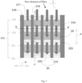
- An array substrate 1 is described according to embodiments of the present disclosure with reference to Figs. 1-4 as below.
- the array substrate 1 includes a base substrate 10 and a pixel define layer 30.
- the pixel define layer 30 is arranged on the base substrate 10.
- the pixel define layer 30 defines a plurality of pixels 20 arranged in an array.
- the pixel define layer 30 may have through holes 25.
- the pixels 20 may be located in the through holes 25 respectively.
- the thickness at different areas of the pixel define layer 30 may be inconsistent.
- the pixel define layer 30 further comprises a plurality of thickness thinning regions 312.
- the thickness thinning region 312 is suitable for guiding fillers for an encapsulating layer to flow.
- a pixel define layer 30 can be laid on a surface of one side of the base substrate 10.
- the pixel define layer 30 includes a plurality of thickness thinning regions 312.
- the thicknesses or heights of the areas defined by the thickness thinning regions 312 on the array substrate 1 are smaller than those of the other areas of the array substrate 1.
- the "thickness" or “height” of the pixel define layer as used herein is measured from the surface of the base substrate facing the pixel define layer.
- An array substrate 1 is provided according to one embodiment of the present disclosure.
- a pixel definition layer 30 is laid on the substrate 10.
- a plurality of pixel grids 20 is defined by the pixel define layer 30.
- the pixel define layer 30 further comprises a plurality of thickness thinning regions 312.
- the thickness thinning regions 312 can guide flow direction of fillers for the encapsulating layer 40 so that fillers for the encapsulating layer 40 can be more uniformly filled, thereby preventing situations in which fillers for the encapsulating layer 40 are excessively filled or not fully filled, which cause poor performance of an OLED or other devices on the array substrate.
- the pixel define layer 30 includes a plurality of first spacing parts 310 and a plurality of second spacing parts 320 intersecting the plurality of the first spacing parts. That is, the first spacing parts 310 are arranged along direction a and the second spacing parts 320 are arranged along direction b. Direction a and direction b are perpendicular to each other. The portion of the second spacing part between two adjacent first spacing parts is termed as a second spacing sub-part 321. Each of the second spacing parts 320 includes a plurality of second spacing sub-parts 321 along direction b.
- the plurality of first spacing parts 310 defines a plurality of arrangement regions 311. The arrangement region 311 is defined by any of two adjacent first spacing parts 310.
- the second spacing sub-parts 321 form thickness thinning regions 312. At least one of the plurality of the arrangement regions 311 includes a plurality of second spacing sub-parts 321 and a plurality of pixels along direction a.
- the plurality of first spacing parts 310 may be distributed at intervals.
- the plurality of the second spacing parts 320 form thickness thinning regions 312 of the array substrate 1. That is, a thickness thinning region includes a plurality of second spacing sub-parts 321 along direction a.
- the pixels 20 may be located between every two adjacent second spacing sub-parts 321. In accordance with the claimed invention, some of the pixels 20 are located between two adjacent second spacing sub-parts 321. Therefore, the positions of the pixels 20 are defined by the plurality of the first spacing parts 310 and the second spacing sub-parts 321.
- the height of the second spacing part 320 is smaller than the height of the first spacing part 310. That is, the distance between the side of the second spacing part 320 away from the base substrate 10 and the base substrate 10 is smaller than the distance between the side of the first spacing part 310 away from the base substrate 10 and the base substrate 10. As such, fillers for the encapsulating layer 40 can flow along the thickness thinning regions 312 defined by the first spacing parts 310.
- the surface of a free end of the first spacing part 310 may have an arc-shaped surface. That is, the surface of one side of the first spacing part 310 away from the base substrate 10 may be formed as an arc-shaped surface. As such, fillers for the encapsulating layer 40 can smoothly flow through the arc-shaped surface, thereby facilitating fillers for the encapsulating layer 40 being fully filled in the whole area needed to be filled. Further, the arc-shaped surface protrudes in a direction away from the base substrate 10. In other words, along a width direction of the first spacing part 310, from the middle to the two sides of the arc-shaped surface, the distance between the arc-shaped surface and the base substrate 10 is gradually reduced. If the first spacing part 310 is cut in a direction perpendicular to the extension direction of the first spacing part 310, the shape of the cross section of the first spacing part 310 at any position may be the same.
- the surface of the free end of the first spacing part 310 may be a plane or a flat surface. That is, the surface of the side of the first spacing part 310 away from the base substrate 10 is formed as a plane or a flat surface. In other words, the distance between any position on the surface of the first spacing part 310 away from the base substrate 10 to the base substrate 10 is equal. Resistance of a plane to a fluid is small, so fillers for the encapsulating layer 40 can quickly flow on the plane, thereby increasing filling rate. Meanwhile, a transition from the first spacing part 310 to the base substrate 10 is not smooth, thereby facilitating fillers for the encapsulating layer 40 being filled into designated areas.
- a surface of a free end of the second spacing part 320 may be an arc surface or a plane.
- the surface of the side of the second spacing part 320 away from the base substrate 10 may be formed as a plane or a flat surface, thereby facilitating fillers for the encapsulating layer 40 being filled into designated areas.
- the surface of the second spacing part 320 away from the side of the base substrate 10 may also be formed as an arc-shaped surface. As such, fillers for the encapsulating layer 40 can smoothly flow through the arc-shaped surface, thereby facilitating the fillers for the encapsulating layer 40 being filled into the whole area needed to be filled.
- the first spacing part 310 is a rectangular strip.
- a length direction of the first spacing part 310 is a first direction a.
- a plurality of the first spacing parts 310 is distributed in parallel at intervals along a second direction b.
- One of the first direction a and the second direction b is the length direction of the substrate 10 and the other is the width direction of the base substrate 10.
- the plurality of first spacing parts 310 can be arranged in parallel at intervals along the width direction of the substrate 10. Any one of the first spacing parts 310 may be rectangular.
- the length direction of the rectangle may extend along the length direction of the base substrate 10.
- the plurality of the first spacing parts 310 may be arranged in parallel at intervals along the length direction of the base substrate 10. Any one of the first spacing parts 310 may be rectangular. The length direction of the rectangle may extend along the width direction of the base substrate 10. As such, fillers for the encapsulating layer 40 can be guided to flow along straight lines.
- the distance between the two adjacent first spacing parts 310 may be gradually changed, for example, increased or decreased. That is, from one end to the other end of the array substrate along the second direction b, the distance between every two adjacent first spacing parts 310 can be gradually increased or gradually decreased.
- first spacing parts 310 can be arranged according to an arrangement of the pixel grids.
- the distance between any two adjacent first spacing parts 310 may be equal.
- a plurality of first spacing parts 310 are uniformly distributed on the substrate 10 at intervals, thereby facilitating uniform arrangement of the pixel grids.
- a plurality of the second spacing parts 320 located in the same arrangement region 311 are distributed at intervals along the first direction a.
- the plurality of the second spacing parts 320 form a plurality of rows.
- the plurality of second spacing parts 320 can guide the encapsulating layer 40 to flow along a straight line.
- the distance between the two adjacent second spacing parts 320 is gradually increased.
- the distance between every two adjacent second spacing parts 320 can be gradually increased or gradually decreased.
- the arrangement mode of the pixel grids can be increased.
- the height of the plurality of the second spacing parts 320 is gradually decreased, as shown in Fig. 2B . From one end to the other end of the base substrate along the first direction a, the heights of the second spacing parts 320 are gradually decreased or gradually increased. Fillers for the encapsulating layer 40 are adapted to flow from one end to the other end of the base substrate along the first direction a. In a flow direction of the encapsulating layer 40, for any two adjacent second spacing parts 320, the height of the second spacing part 320 located downstream is lower than the height of the second spacing part 320 located upstream.
- fillers for the encapsulating layer 40 can be better guided to flow from one side of the base substrate 10 to the other side of the base substrate 10 along the first direction a.
- the height of the second spacing parts 320 is distributed in a stepped mode.
- the distance between any two of the adjacent second spacing parts 320 is equal.
- the plurality of the second spacing parts 320 is uniformly distributed in the arrangement region 311, thereby, improving uniformity of the pixel define layer and facilitating arrangement uniformity of the pixel grids.
- the base substrate 10 may be a rectangular flat plate.
- the first spacing part 310 may be in a strip shape.
- the plurality of first spacing part parts 310 may extend along the length direction (or width direction) of the base substrate 10 and may be arranged in parallel at equal intervals.
- the length extension direction of any of the first spacing parts 310 may be the same as the width direction (or length direction) of the base substrate 10 so that a plurality of strip-shaped arrangement regions 311 can be defined on the base substrate 10.
- the plurality of second spacing parts 320 may be in a strip shape.
- the length extension direction of the second spacing part 320 may be perpendicular to the length extension direction of the arrangement region 311.
- the plurality of the second spacing parts 320 may be distributed at equal intervals on the arrangement region 311.
- the pixel grids 20 may be located in the intervals of either of the two second spacing parts 320. As shown in Fig. 2 and Fig. 4 , the pixel grid 20 may be rectangular.
- the pixel grid 20 has two pairs of opposite sides. One pair of opposite sides may be respectively in contact with two adjacent first spacing parts 310. The other pair of opposite sides may be respectively in contact with two adjacent second spacing parts 320.
- the thickness of the pixel define layer 30 may be greater than or equal to 2 micrometers.
- the thicknesses of the first spacing part 310 and the second spacing part 320 are greater than or equal to 2 micrometers. As such, light emitting elements above the pixel define layer 30 can be prevented from contacting the anode below the pixel define layer 30.
- a display panel is provided according to one embodiment of the present disclosure.
- the display panel includes an array substrate and a cover plate.
- the array substrate may be any one of the array substrates 1 according to one embodiment of the present disclosure.
- the cover plate is stacked on the base substrate 10.
- An encapsulating layer 40 is arranged between the cover plate and the array substrate 1.
- the side of the substrate 10 provided with a pixel define layer 30 is opposite to the cover plate.
- the encapsulating layer 40 can be arranged between the array substrate 1 and the cover plate so that the array substrate 1 is isolated from the cover plate.
- Fillers for the encapsulating layer 40 can have fluidity. Fillers for the encapsulating layer 40 can flow to any gap between the array substrate 1 and the cover plate.
- the encapsulating layer 40 may have adhesion capability so that the array substrate 1 and the cover plate can be packaged together.
- the pixel define layer 30 is laid on the base substrate 10.
- a plurality of pixel grids 20 are defined by the pixel define layer 30.
- the pixel define layer 30 further comprises a plurality of thickness thinning regions 312.
- the thickness thinning regions 312 can guide the flow direction of the fillers for the encapsulating layer 40, so that fillers for the encapsulating layer 40 can be filled uniformly, thereby preventing fillers for the encapsulating layer 40 from being filled excessively or not fully, which causes invalid or poor performance of the display panel.
- spacers may be disposed on a side of the cover plate facing the array substrate 1. Orthographic projections of the spacers on the array substrate 1 do not overlap the thickness thinning regions 312.
- the spacers (PS pattern) are disposed toward the first spacing parts 310.
- the spacers (PS pattern) may be opposite to the first spacing parts 310.
- the spacer (PS pattern) may be in a circular truncated cone shape. In one embodiment, a surface of a free end of the circular truncated cone may protrude towards the first spacing part 310. As such, a packaging height of the OLED can be easily realized.
- the display panel may be an OLED display panel.
- the OLED display panel has advantages such as thin, light, wide viewing angle, active light emitting, continuous and adjustable color of emitting light, low cost, fast response speed, low energy consumption, low driving voltage, wide working temperature range, simple production process, high light emitting efficiency, and flexible display and the like.
- a manufacturing method of the display panel includes the following steps.
- a color filter is formed on the base substrate 10.
- a pixel define layer 30 is then formed on the base substrate 10.
- the pixel define layer 30 defines a plurality of pixel grids 20 arranged in an array.
- the pixel define layer 30 further comprises a plurality of thickness thinning regions 312.
- the thicknesses or heights of the thickness thinning regions 312 are smaller than those of other regions of the pixel define layer 30.
- the thickness thinning regions 312 are suitable for guiding fillers for the encapsulating layer 40 to flow.
- a cover plate and the base substrate are arranged in a layered structure. Fillers for the encapsulating layer 40 are filled between the cover plate and the array substrate 1.
- a pixel define layer 30 is laid on the substrate 10.
- a plurality of pixel grids 20 is defined by the pixel define layer 30.
- the pixel define layer 30 further comprises a plurality of thickness thinning regions 312.
- the thickness thinning regions 312 can guide flow direction of the fillers for the encapsulating layer 40 so that the fillers for the encapsulating layer 40 can be more uniformly filled, thereby preventing fillers for the encapsulating layer 40 from being filled excessively or not fully, which causes poor performance of the display panel such as an OLED display panel.
- the manufacturing method comprises the following steps: A color filter is formed on the base substrate.
- a pixel define layer 30 is manufactured on the base substrate 10.
- an electroluminescence (EL) and a cathode are manufactured on the pixel define layer 30.
- a black matrix (BM) pattern, a color film (CF) graph, an optical adhesive (OC) graph, a metal graph, a PS graph and an ITO graph are manufactured on the cover plate.
- the base substrate 10 and the cover plate are then packaged.
- the ITO pattern on the PS pattern is connected with the cathode to form an auxiliary cathode.
- fillers for an encapsulating layer 40 are filled between the base substrate 10 and the cover plate.
- a color filter is laid on the surface of the substrate 10. Then, a pixel define layer 30 is laid on the color filter. The pixel define layer 30 can define positions of the pixel grids 20. Then, an Electroluminescence (EL) and a cathode are formed on the pixel define layer 30. Separately, a black matrix (BM) pattern and a color film (CF) pattern are manufactured on the cover plate. An Optical Adhesive (OC) pattern is laid on the BM pattern and the CF pattern for encapsulating. Then a metal pattern (metal layer) is manufactured on the surface of OC pattern.
- BM black matrix
- CF color film
- PS patterns spacers
- ITO Indium Tin Oxide
- the side of the base substrate 10 on which the cathode is formed may face the ITO pattern formed on the cover plate so that the cathode may be connected to the ITO.
- the encapsulating layer 40 is then filled in the interval between the array substrate 1 and the cover plate.
- the pixel define layer 30 may be formed by masking and exposure.
- the first spacing part 310 and the second spacing part 320 can both be formed by masking and exposure.
- the masking is to mask a processed image by a selected image, pattern or object, partly or in whole, so as to control the area or process of the image processing, thereby improving manufacturing accuracy of the pixel define layer 30.
- a display apparatus is provided according to one embodiment of the present disclosure.
- the display apparatus comprises an array substrate 1 according to one embodiment of the present disclosure.
- the pixel define layer 30 is laid on the base substrate 10.
- a plurality of pixel grids 20 is defined by the pixel define layer 30.
- the pixel define layer 30 further comprises a plurality of thickness thinning regions 312.
- the thickness thinning regions 312 can guide the flow direction of the fillers for the encapsulating layer 40, so that the fillers for the encapsulating layer 40 can be more uniformly filled, thereby preventing fillers for the encapsulating layer 40 from being filled excessively or not fully, which causes poor performance of the display panel.
- the array substrate 1 is described in detail below with reference to Figs. 1-4 according to one embodiment of the present disclosure.
- the array substrate 1 comprises a base substrate 10 and a pixel define layer 30.
- the base substrate 10 may be a rectangular flat plate.
- the pixel define layer 30 can be formed by masking and polishing.
- the pixel define layer 30 may include a plurality of first spacing parts 310 and a plurality of second spacing parts 320.
- the first spacing part 310 is in a strip shape.
- the plurality of the first spacing parts 310 may be arranged in parallel along the length direction of the base substrate 10 at equal intervals.
- the length extension direction of any of the first spacing parts 310 may be consistent with the width direction of the base substrate 10, so that a plurality of strip-shaped thickness thinning regions 312 can be defined on the base substrate 10.
- the surface of the free end of the first spacing part 310 may be an arc-shaped surface.
- the arc-shaped surface protrudes in a direction away from the base substrate 10.
- the shape of a cross section of the first spacing part 310 cut at any position along the width direction of the base substrate 10 is the same.
- the plurality of the second spacing parts 320 may be in a strip shape.
- the length extension direction of the second spacing parts 320 may be perpendicular to the length extension direction of the thickness thinning regions 312.
- the plurality of the second spacing parts 320 may be distributed at equal intervals in the thickness thinning regions 312.
- the surfaces of the free ends of the second spacing parts 320 may be arc-shaped surfaces or planes.
- a plurality of pixel grids 20 are arranged in the thickness thinning regions 312 and located in intervals between any two second spacing parts 320.
- the pixel grids 20 may be rectangular.
- the pixel grid 20 has two pairs of opposite sides. One pair of opposite sides may be respectively in contact with two adjacent first spacing parts 310, and the other pair of opposite sides may be respectively in contact with two adjacent second spacing parts 320.
- the thickness of the area where the pixel grids 20 are located is smaller than the thickness of the area where the second spacing parts 320 are located.
- the thickness of the area where the second spacing parts 320 are located is smaller than the thickness of the area where the first spacing parts 310 are located.
- the thicknesses of the first spacing parts 310 and the thickness of the second spacing parts 320 are both greater than 2 micrometers.
- the array substrate 1 is provided according to one embodiment of the present disclosure.
- a pixel define layer 30 is laid on the base substrate 10.
- a plurality of pixel grids 20 is defined by the pixel define layer 30.
- the pixel define layer 30 further comprises a plurality of thickness thinning regions 312.
- the thickness thinning regions 312 can guide the flow direction of the fillers for the encapsulating layer 40, so that fillers for the encapsulating layer 40 can be more uniformly filled, thereby preventing the encapsulating layer 40 from being excessively filled or not fully filled, which will cause poor performance of components on the array substrate such as an OLED or other devices.
- references made to the term "one embodiment,” “some embodiments,” and “exemplary embodiments,” “example,” and “specific example,” or “some examples” and the like are intended to refer that specific features and structures, materials or characteristics described in connection with the embodiment or example that are included in at least one embodiment or example of the present disclosure.
- the schematic expression of the terms does not necessarily refer to the same embodiment or example.
- the specific features, structures, materials or characteristics described may be included in any suitable manner in any one or more embodiments or examples.
Landscapes
- Engineering & Computer Science (AREA)
- Microelectronics & Electronic Packaging (AREA)
- Physics & Mathematics (AREA)
- Optics & Photonics (AREA)
- Geometry (AREA)
- Electroluminescent Light Sources (AREA)
- Devices For Indicating Variable Information By Combining Individual Elements (AREA)
Claims (14)
- Array-Substrat, umfassend:ein Basissubstrat (10); undeine Pixeldefinitionsschicht (30) auf dem Basissubstrat, wobei die Pixeldefinitionsschicht eine Vielzahl von dickenausdünnenden Bereichen (312) umfasst,wobei die dickenausdünnenden Bereiche (312) eine geringere Höhe als andere Flächen der Pixeldefinitionsschicht (30) auf dem Basissubstrat aufweisen, und die Vielzahl der dickenausdünnenden Bereiche (312) konfiguriert sind, um den Fluss von Füllstoffen zu leiten, um eine Einkapselungsschicht (40) auf der Pixeldefinitionsschicht (30) auszubilden;wobei die Pixeldefinitionsschicht (30) Folgendes umfasst:eine Vielzahl von ersten Beabstandungselementen (310); undeine Vielzahl von zweiten Beabstandungselementen (320), die die Vielzahl der ersten Beabstandungselemente (310) überschneiden, wobei jedes der Vielzahl der zweiten Beabstandungselemente (320) eine Vielzahl von zweiten Beabstandungsunterelementen (321) umfasst, wobei eine Höhe von jedem der Vielzahl der zweiten Beabstandungsunterelemente (321) kleiner ist als die von jedem der Vielzahl der ersten Beabstandungselemente (310), und jeder der dickenausdünnenden Bereiche (312) eine Vielzahl der zweiten Beabstandungsunterelemente (321) zwischen zwei benachbarten ersten Beabstandungselementen (310) umfasst;wobei jedes der Vielzahl der ersten Beabstandungselemente (310) eine rechteckige Streifenform aufweist, eine Längsrichtung der ersten Beabstandungselemente (310) eine erste Richtung (a) ist und die Vielzahl der ersten Beabstandungselemente (310) in Intervallen in einer zweiten Richtung (b) verteilt sind; unddie Pixeldefinitionsschicht (30) eine Vielzahl von Pixelrastern (20) definiert, die in einem Array angeordnet sind, und zumindest einige der Pixelraster (20) zwischen zwei benachbarten zweiten Beabstandungselementen (320) angeordnet sind, wobei die Höhen der Vielzahl der zweiten Beabstandungsunterelemente (321) in einem gleichen dickenausdünnenden Bereich (312) entlang der ersten Richtung (a) graduell abnehmen oder zunehmen.
- Array-Substrat nach Anspruch 1,
wobei optional eine der ersten Richtung (a) und der zweiten Richtung (b) eine Längsrichtung des Basissubstrats ist und die andere eine Breitenrichtung des Basissubstrats ist. - Array-Substrat nach Anspruch 2, wobei
jedes der Pixelraster (20) zwei Paare gegenüberliegenden Seiten aufweist, wobei ein Paar der gegenüberliegenden Seiten jeweils in Kontakt mit zwei benachbarten ersten Beabstandungselementen (310) steht und das andere Paar der gegenüberliegenden Seiten jeweils in Kontakt mit zwei benachbarten zweiten Beabstandungsunterelementen (321) steht. - Array-Substrat nach Anspruch 2, wobei eine Oberfläche jedes der Vielzahl der ersten Beabstandungselemente (310) eine bogenförmige Oberfläche oder eine flache Oberfläche ist.
- Array-Substrat nach Anspruch 2, wobei eine Oberfläche jedes der Vielzahl der zweiten Beabstandungsunterelemente (321) eine bogenförmige Oberfläche oder eine flache Oberfläche ist.
- Array-Substrat nach Anspruch 1, wobei ein Abstand zwischen zwei beliebigen benachbarten zweiten Beabstandungsunterelementen (321) in einem gleichen dickenausdünnenden Bereich (312) entlang der ersten Richtung (a) graduell zunimmt oder abnimmt.
- Array-Substrat nach Anspruch 1, wobei ein Abstand zwischen zwei beliebigen benachbarten zweiten Beabstandungsunterelementen (321) in einem gleichen dickenausdünnenden Bereich (312) entlang der ersten Richtung (a) gleich ist.
- Array-Substrat nach Anspruch 1, wobei die Dicke jedes der Vielzahl der zweiten Beabstandungselemente (320) größer als oder gleich 2 Mikrometer ist.
- Anzeigetafel, umfassend:das Array-Substrat (1) nach irgendeinem der Ansprüche 1-8 undeine über dem Array-Substrat (1) gestapelte Abdeckplatte, wobei die Einkapselungsschicht (40) zwischen der Abdeckplatte und dem Array-Substrat (1) angeordnet ist.
- Anzeigetafel nach Anspruch 9, wobei Abstandshalter (PS) auf einer Seite der Abdeckplatte angeordnet sind, die dem Array-Substrat (1) zugewandt ist, und die orthographische Projektion der Abstandshalter (PS) auf das Array-Substrat (1) die dickenausdünnenden Bereiche (312) nicht überlappt.
- Anzeigetafel nach Anspruch 9, wobei die Anzeigetafel eine OLED-Anzeigetafel ist.
- Verfahren zur Herstellung einer Anzeigetafel nach Anspruch 1, wobei das Verfahren Folgendes umfasst:Ausbilden einer Pixeldefinitionsschicht (30) auf einem Basissubstrat (10), wobei die Pixeldefinitionsschicht eine Vielzahl von Pixelrastern (20) definiert, die in einem Array-Modus angeordnet sind,wobei die Pixeldefinitionsschicht (30) ferner eine Vielzahl von dickenausdünnenden Bereichen (312) umfasst,wobei die dickenausdünnenden Bereiche (312) eine geringere Höhe als andere Flächen der Pixeldefinitionsschicht (30) aufweisen und die dickenausdünnenden Bereiche (312) konfiguriert sind, um den Fluss von Füllstoffen zu leiten, um eine Einkapselungsschicht (40) auf der Pixeldefinitionsschicht (30) auszubilden;wobei die Pixeldefinitionsschicht (30) Folgendes umfasst:eine Vielzahl von ersten Beabstandungselementen (310); undeine Vielzahl von zweiten Beabstandungselementen (320), die die Vielzahl der ersten Beabstandungselemente (310) überschneiden, wobei jedes der Vielzahl der zweiten Beabstandungselemente (320) eine Vielzahl von zweiten Beabstandungsunterelementen (321) umfasst, wobei eine Höhe von jedem der Vielzahl der zweiten Beabstandungsunterelemente (321) kleiner ist als die von jedem der Vielzahl der ersten Beabstandungselemente (310), und jeder der dickenausdünnenden Bereiche (312) eine Vielzahl der zweiten Beabstandungsunterelemente (321) zwischen zwei benachbarten ersten Beabstandungselementen (310) umfasst;wobei jedes der Vielzahl der ersten Beabstandungselemente (310) eine rechteckige Streifenform aufweist, eine Längsrichtung der ersten Beabstandungselemente (310) eine erste Richtung (a) ist und die Vielzahl der ersten Beabstandungselemente (310) in Intervallen in einer zweiten Richtung (b) verteilt sind; unddie Pixeldefinitionsschicht (30) eine Vielzahl von Pixelrastern (20) definiert, die in einem Array angeordnet sind, und zumindest einige der Pixelraster (20) zwischen zwei benachbarten zweiten Beabstandungselementen (320) angeordnet sind, wobei die Höhen der Vielzahl der zweiten Beabstandungsunterelemente (321) in einem gleichen dickenausdünnenden Bereich (312) entlang der ersten Richtung (a) graduell abnehmen oder zunehmen.
- Verfahren zur Herstellung der Anzeigetafel nach Anspruch 12, wobei die Pixeldefinitionsschicht (30) durch Maskieren und Belichten ausgebildet wird.
- Anzeigevorrichtung umfassend das Array-Substrat (1) nach irgendeinem der Ansprüche 1-8.
Applications Claiming Priority (2)
| Application Number | Priority Date | Filing Date | Title |
|---|---|---|---|
| CN201710954861.7A CN109671738B (zh) | 2017-10-13 | 2017-10-13 | 阵列基板、显示面板及其制作方法和显示装置 |
| PCT/CN2018/079445 WO2019071914A1 (en) | 2017-10-13 | 2018-03-19 | NETWORK SUBSTRATE, DISPLAY PANEL, DISPLAY APPARATUS, AND METHOD FOR MANUFACTURING THE SAME |
Publications (3)
| Publication Number | Publication Date |
|---|---|
| EP3695441A1 EP3695441A1 (de) | 2020-08-19 |
| EP3695441A4 EP3695441A4 (de) | 2021-07-21 |
| EP3695441B1 true EP3695441B1 (de) | 2024-09-11 |
Family
ID=66100365
Family Applications (1)
| Application Number | Title | Priority Date | Filing Date |
|---|---|---|---|
| EP18780012.3A Active EP3695441B1 (de) | 2017-10-13 | 2018-03-19 | Arraysubstrat, anzeigetafel, anzeigevorrichtung und herstellungsverfahren dafür |
Country Status (5)
| Country | Link |
|---|---|
| US (2) | US11424303B2 (de) |
| EP (1) | EP3695441B1 (de) |
| JP (1) | JP7031954B2 (de) |
| CN (1) | CN109671738B (de) |
| WO (1) | WO2019071914A1 (de) |
Families Citing this family (5)
| Publication number | Priority date | Publication date | Assignee | Title |
|---|---|---|---|---|
| CN110323261B (zh) * | 2019-07-04 | 2022-09-13 | 京东方科技集团股份有限公司 | 一种显示基板及其制作方法、显示装置 |
| CN110534547A (zh) * | 2019-08-02 | 2019-12-03 | 武汉天马微电子有限公司 | 显示装置及其制作方法 |
| CN110416433B (zh) * | 2019-08-02 | 2022-04-08 | 京东方科技集团股份有限公司 | 像素界定单元、像素界定结构、显示结构及显示装置 |
| CN116347937A (zh) * | 2023-01-16 | 2023-06-27 | 昆山国显光电有限公司 | 一种显示面板、显示面板制作方法及显示设备 |
| CN117148612B (zh) * | 2023-08-30 | 2025-02-07 | 长沙惠科光电有限公司 | 阵列基板及其显示面板 |
Citations (1)
| Publication number | Priority date | Publication date | Assignee | Title |
|---|---|---|---|---|
| EP2151868B1 (de) * | 2007-05-28 | 2017-08-09 | Joled Inc. | Organische el-vorrichtung und -anzeige |
Family Cites Families (54)
| Publication number | Priority date | Publication date | Assignee | Title |
|---|---|---|---|---|
| US6198093B1 (en) * | 1998-11-19 | 2001-03-06 | Xerox Corporation | Electro optical devices with reduced filter thinning on the edge pixel photosites and method of producing same |
| JP4590663B2 (ja) * | 1999-10-29 | 2010-12-01 | セイコーエプソン株式会社 | カラーフィルタの製造方法 |
| TWI258317B (en) * | 2002-01-25 | 2006-07-11 | Semiconductor Energy Lab | A display device and method for manufacturing thereof |
| JP2003229247A (ja) | 2002-02-04 | 2003-08-15 | Sanyo Electric Co Ltd | 有機エレクトロルミネッセンス装置 |
| US7307381B2 (en) * | 2002-07-31 | 2007-12-11 | Dai Nippon Printing Co., Ltd. | Electroluminescent display and process for producing the same |
| KR100508002B1 (ko) | 2002-09-03 | 2005-08-17 | 엘지.필립스 엘시디 주식회사 | 노즐코팅을 이용한 유기 전계 발광 소자 제조 방법 |
| KR100705312B1 (ko) * | 2004-03-22 | 2007-04-10 | 엘지전자 주식회사 | 유기 전계발광소자 및 그 제조방법 |
| US7276453B2 (en) * | 2004-08-10 | 2007-10-02 | E.I. Du Pont De Nemours And Company | Methods for forming an undercut region and electronic devices incorporating the same |
| KR100683695B1 (ko) * | 2004-11-11 | 2007-02-15 | 삼성에스디아이 주식회사 | 유기전계 발광표시장치 |
| KR20070050685A (ko) | 2005-11-11 | 2007-05-16 | 삼성전자주식회사 | 컬러 필터 기판의 제조 방법 및 이를 포함하는 액정 표시장치의 제조 방법 |
| US7633218B2 (en) * | 2006-09-29 | 2009-12-15 | Eastman Kodak Company | OLED device having improved lifetime and resolution |
| US8154032B2 (en) * | 2007-07-23 | 2012-04-10 | Seiko Epson Corporation | Electrooptical device, electronic apparatus, and method for producing electrooptical device |
| JP2009043499A (ja) * | 2007-08-08 | 2009-02-26 | Canon Inc | 有機el素子用基板及びその製造方法 |
| US8410476B2 (en) * | 2007-09-28 | 2013-04-02 | Sharp Kabushiki Kaisha | Organic electroluminescent display device and production method thereof |
| KR100995066B1 (ko) * | 2009-01-07 | 2010-11-18 | 삼성모바일디스플레이주식회사 | 유기 발광 표시 장치 및 그 제조 방법 |
| KR100989133B1 (ko) * | 2009-01-07 | 2010-10-20 | 삼성모바일디스플레이주식회사 | 유기 발광 표시 장치 |
| KR100989135B1 (ko) | 2009-01-07 | 2010-10-20 | 삼성모바일디스플레이주식회사 | 유기 발광 표시 장치 |
| JP2010287421A (ja) * | 2009-06-11 | 2010-12-24 | Toppan Printing Co Ltd | 有機el装置及びその製造方法 |
| KR101107158B1 (ko) * | 2009-07-10 | 2012-01-25 | 삼성모바일디스플레이주식회사 | 유기 발광 표시 장치 및 그 제조 방법 |
| KR101084274B1 (ko) * | 2009-10-08 | 2011-11-16 | 삼성모바일디스플레이주식회사 | 유기 발광 표시 장치 및 그 제조 방법 |
| JP2011181305A (ja) | 2010-03-01 | 2011-09-15 | Toppan Printing Co Ltd | 有機エレクトロルミネッセンス素子及びその製造方法 |
| TWI503043B (zh) * | 2010-04-13 | 2015-10-01 | Au Optronics Corp | 電激發光顯示面板 |
| EP2618638A4 (de) * | 2011-04-22 | 2013-08-14 | Panasonic Corp | Organische el-anzeigetafel und verfahren zu ihrer herstellung |
| TW201338620A (zh) * | 2012-03-08 | 2013-09-16 | Innocom Tech Shenzhen Co Ltd | 顯示裝置及製造其之方法 |
| KR101955621B1 (ko) * | 2012-09-21 | 2019-05-31 | 삼성디스플레이 주식회사 | 유기발광 표시패널 및 그 제조방법 |
| KR101993331B1 (ko) | 2013-01-03 | 2019-06-27 | 삼성디스플레이 주식회사 | 유기발광표시장치 및 그 제조방법 |
| JP2014132525A (ja) * | 2013-01-04 | 2014-07-17 | Japan Display Inc | 有機el表示装置 |
| KR20140090458A (ko) | 2013-01-09 | 2014-07-17 | 삼성디스플레이 주식회사 | 유기 발광 표시 장치 및 이의 제조 방법 |
| KR20140108025A (ko) * | 2013-02-28 | 2014-09-05 | 삼성디스플레이 주식회사 | 유기발광 디스플레이 장치 및 그 제조방법 |
| JP5991490B2 (ja) * | 2013-03-22 | 2016-09-14 | 株式会社ジャパンディスプレイ | 有機エレクトロルミネッセンス表示装置 |
| CN103311269B (zh) * | 2013-05-29 | 2017-06-09 | 京东方科技集团股份有限公司 | 一种oled像素限定结构及其制作方法 |
| KR102090713B1 (ko) * | 2013-06-25 | 2020-03-19 | 삼성디스플레이 주식회사 | 가요성 표시 패널 및 상기 가요성 표시 패널의 제조 방법 |
| US9494792B2 (en) * | 2013-07-30 | 2016-11-15 | Global Oled Technology Llc | Local seal for encapsulation of electro-optical element on a flexible substrate |
| TWI545735B (zh) * | 2013-09-09 | 2016-08-11 | Japan Display Inc | Organic electroluminescent display device and manufacturing method thereof |
| JP2015138180A (ja) | 2014-01-23 | 2015-07-30 | 凸版印刷株式会社 | カラーフィルタ、液晶表示パネルおよび液晶表示装置 |
| US9755193B2 (en) * | 2014-02-10 | 2017-09-05 | Joled Inc. | Bank repair method, organic EL display device, and production method for same |
| JP6332769B2 (ja) | 2014-02-21 | 2018-05-30 | 株式会社Joled | 有機発光デバイスと有機表示装置 |
| WO2015155971A1 (ja) | 2014-04-08 | 2015-10-15 | 株式会社Joled | 有機発光デバイスおよびその製造方法 |
| JP2015207526A (ja) | 2014-04-23 | 2015-11-19 | 株式会社Joled | 有機発光デバイスの機能層の形成方法 |
| CN104022139B (zh) * | 2014-05-30 | 2016-03-30 | 京东方科技集团股份有限公司 | 一种有机电致发光显示面板及显示装置 |
| CN104409647A (zh) | 2014-11-14 | 2015-03-11 | 京东方科技集团股份有限公司 | 一种像素单元及其制作方法、发光器件、显示装置 |
| KR20160066650A (ko) * | 2014-12-02 | 2016-06-13 | 삼성디스플레이 주식회사 | 표시 장치의 제조 방법 및 표시 장치 |
| KR102381289B1 (ko) * | 2015-02-26 | 2022-03-31 | 삼성디스플레이 주식회사 | 유기 발광 표시 장치 |
| JP6649714B2 (ja) * | 2015-08-04 | 2020-02-19 | 株式会社Joled | バンク補修方法、有機el表示装置の製造方法および有機el表示装置 |
| JP6685675B2 (ja) | 2015-09-07 | 2020-04-22 | 株式会社Joled | 有機el素子、それを用いた有機el表示パネル、及び有機el表示パネルの製造方法 |
| US10304813B2 (en) * | 2015-11-05 | 2019-05-28 | Innolux Corporation | Display device having a plurality of bank structures |
| CN106876424A (zh) * | 2015-12-14 | 2017-06-20 | 上海和辉光电有限公司 | 一种有机发光显示器及其制备方法 |
| CN105470409A (zh) | 2016-01-04 | 2016-04-06 | 京东方科技集团股份有限公司 | 一种oled封装结构及其制作方法、显示器件 |
| JP6741431B2 (ja) * | 2016-01-25 | 2020-08-19 | 株式会社Joled | 表示パネル及びその製造方法 |
| JP6727844B2 (ja) | 2016-02-25 | 2020-07-22 | 株式会社ジャパンディスプレイ | 表示装置 |
| JP2017174553A (ja) * | 2016-03-22 | 2017-09-28 | 株式会社ジャパンディスプレイ | 表示装置 |
| CN105762172B (zh) * | 2016-05-16 | 2019-03-15 | 京东方科技集团股份有限公司 | 一种阵列基板及其制备方法、显示面板及其驱动方法 |
| CN107104127B (zh) * | 2017-04-27 | 2019-11-22 | 上海天马有机发光显示技术有限公司 | 有机发光显示面板和显示装置 |
| CN107104130A (zh) | 2017-05-26 | 2017-08-29 | 京东方科技集团股份有限公司 | 一种oled显示基板及制备方法、显示面板及显示装置 |
-
2017
- 2017-10-13 CN CN201710954861.7A patent/CN109671738B/zh active Active
-
2018
- 2018-03-19 US US16/082,396 patent/US11424303B2/en active Active
- 2018-03-19 WO PCT/CN2018/079445 patent/WO2019071914A1/en not_active Ceased
- 2018-03-19 EP EP18780012.3A patent/EP3695441B1/de active Active
- 2018-03-19 JP JP2018566950A patent/JP7031954B2/ja active Active
-
2022
- 2022-07-27 US US17/874,653 patent/US12048202B2/en active Active
Patent Citations (1)
| Publication number | Priority date | Publication date | Assignee | Title |
|---|---|---|---|---|
| EP2151868B1 (de) * | 2007-05-28 | 2017-08-09 | Joled Inc. | Organische el-vorrichtung und -anzeige |
Also Published As
| Publication number | Publication date |
|---|---|
| US20230042951A1 (en) | 2023-02-09 |
| JP7031954B2 (ja) | 2022-03-08 |
| JP2020537281A (ja) | 2020-12-17 |
| CN109671738B (zh) | 2021-02-05 |
| CN109671738A (zh) | 2019-04-23 |
| US11424303B2 (en) | 2022-08-23 |
| EP3695441A1 (de) | 2020-08-19 |
| US12048202B2 (en) | 2024-07-23 |
| US20210225964A1 (en) | 2021-07-22 |
| WO2019071914A1 (en) | 2019-04-18 |
| EP3695441A4 (de) | 2021-07-21 |
Similar Documents
| Publication | Publication Date | Title |
|---|---|---|
| US12048202B2 (en) | Array substrate including pixel defining layer with spacer parts | |
| KR102420761B1 (ko) | 픽셀 배열 구조 | |
| CN108962953B (zh) | Oled显示面板及oled显示器 | |
| US10886481B2 (en) | Display substrate with angle-adjusting portion, manufacturing method thereof, and display device | |
| CN107068729B (zh) | 像素结构及其制作方法、显示基板和显示装置 | |
| CN108807491B (zh) | 像素排列结构 | |
| CN110047893B (zh) | 一种有机发光二极管显示器及其制作方法 | |
| JP2018170152A (ja) | Oled表示装置の製造方法、マスク及びマスクの設計方法 | |
| CN105552107A (zh) | 一种显示面板、制作方法以及电子设备 | |
| WO2011096030A1 (ja) | 蒸着マスク、蒸着装置及び蒸着方法 | |
| US11024676B2 (en) | Organic light-emitting diode display panel and manufacturing method thereof, and display device | |
| WO2021233070A1 (zh) | 显示基板及其制作方法、显示面板及显示装置 | |
| EP4228017B1 (de) | Anzeigetafel und herstellungsverfahren dafür sowie anzeigevorrichtung | |
| US20200385856A1 (en) | Vapor deposition mask | |
| KR20120041510A (ko) | 유기전계 발광소자 및 이를 제조하기 위한 쉐도우 마스크 | |
| CN113193024A (zh) | 显示面板及其制备方法、显示装置 | |
| CN109817669B (zh) | 一种有机发光二极管显示器 | |
| KR20110108049A (ko) | 유기전계발광소자 및 이의 제조방법 | |
| TWI604600B (zh) | 有機電激發光顯示面板 | |
| KR20090073478A (ko) | 유기전계발광표시장치 및 그의 제조방법 | |
| JP2020510952A (ja) | エレクトロルミネッセンスディスプレイパネル及びその製造方法、表示装置 | |
| CN113299867A (zh) | 显示面板、显示基板及其制备方法 | |
| CN215644554U (zh) | 显示面板及显示基板 | |
| CN101513121A (zh) | 有机发光显示器 | |
| JP2017162547A (ja) | 有機el素子及びその製造方法 |
Legal Events
| Date | Code | Title | Description |
|---|---|---|---|
| STAA | Information on the status of an ep patent application or granted ep patent |
Free format text: STATUS: UNKNOWN |
|
| STAA | Information on the status of an ep patent application or granted ep patent |
Free format text: STATUS: THE INTERNATIONAL PUBLICATION HAS BEEN MADE |
|
| PUAI | Public reference made under article 153(3) epc to a published international application that has entered the european phase |
Free format text: ORIGINAL CODE: 0009012 |
|
| STAA | Information on the status of an ep patent application or granted ep patent |
Free format text: STATUS: REQUEST FOR EXAMINATION WAS MADE |
|
| 17P | Request for examination filed |
Effective date: 20181012 |
|
| AK | Designated contracting states |
Kind code of ref document: A1 Designated state(s): AL AT BE BG CH CY CZ DE DK EE ES FI FR GB GR HR HU IE IS IT LI LT LU LV MC MK MT NL NO PL PT RO RS SE SI SK SM TR |
|
| AX | Request for extension of the european patent |
Extension state: BA ME |
|
| DAV | Request for validation of the european patent (deleted) | ||
| DAX | Request for extension of the european patent (deleted) | ||
| A4 | Supplementary search report drawn up and despatched |
Effective date: 20210617 |
|
| RIC1 | Information provided on ipc code assigned before grant |
Ipc: H01L 27/32 20060101AFI20210611BHEP |
|
| P01 | Opt-out of the competence of the unified patent court (upc) registered |
Effective date: 20230630 |
|
| REG | Reference to a national code |
Ref country code: DE Ref legal event code: R079 Free format text: PREVIOUS MAIN CLASS: H01L0027320000 Ipc: H10K0059800000 Ref country code: DE Ref legal event code: R079 Ref document number: 602018074278 Country of ref document: DE Free format text: PREVIOUS MAIN CLASS: H01L0027320000 Ipc: H10K0059800000 |
|
| GRAP | Despatch of communication of intention to grant a patent |
Free format text: ORIGINAL CODE: EPIDOSNIGR1 |
|
| STAA | Information on the status of an ep patent application or granted ep patent |
Free format text: STATUS: GRANT OF PATENT IS INTENDED |
|
| INTG | Intention to grant announced |
Effective date: 20240507 |
|
| RIC1 | Information provided on ipc code assigned before grant |
Ipc: H10K 102/00 20230101ALN20240423BHEP Ipc: H10K 59/173 20230101ALI20240423BHEP Ipc: H10K 59/122 20230101ALI20240423BHEP Ipc: H10K 59/80 20230101AFI20240423BHEP |
|
| GRAS | Grant fee paid |
Free format text: ORIGINAL CODE: EPIDOSNIGR3 |
|
| GRAA | (expected) grant |
Free format text: ORIGINAL CODE: 0009210 |
|
| STAA | Information on the status of an ep patent application or granted ep patent |
Free format text: STATUS: THE PATENT HAS BEEN GRANTED |
|
| AK | Designated contracting states |
Kind code of ref document: B1 Designated state(s): AL AT BE BG CH CY CZ DE DK EE ES FI FR GB GR HR HU IE IS IT LI LT LU LV MC MK MT NL NO PL PT RO RS SE SI SK SM TR |
|
| REG | Reference to a national code |
Ref country code: GB Ref legal event code: FG4D |
|
| REG | Reference to a national code |
Ref country code: CH Ref legal event code: EP |
|
| REG | Reference to a national code |
Ref country code: DE Ref legal event code: R096 Ref document number: 602018074278 Country of ref document: DE |
|
| REG | Reference to a national code |
Ref country code: IE Ref legal event code: FG4D |
|
| REG | Reference to a national code |
Ref country code: LT Ref legal event code: MG9D |
|
| PG25 | Lapsed in a contracting state [announced via postgrant information from national office to epo] |
Ref country code: NO Free format text: LAPSE BECAUSE OF FAILURE TO SUBMIT A TRANSLATION OF THE DESCRIPTION OR TO PAY THE FEE WITHIN THE PRESCRIBED TIME-LIMIT Effective date: 20241211 |
|
| REG | Reference to a national code |
Ref country code: NL Ref legal event code: MP Effective date: 20240911 |
|
| PG25 | Lapsed in a contracting state [announced via postgrant information from national office to epo] |
Ref country code: GR Free format text: LAPSE BECAUSE OF FAILURE TO SUBMIT A TRANSLATION OF THE DESCRIPTION OR TO PAY THE FEE WITHIN THE PRESCRIBED TIME-LIMIT Effective date: 20241212 Ref country code: FI Free format text: LAPSE BECAUSE OF FAILURE TO SUBMIT A TRANSLATION OF THE DESCRIPTION OR TO PAY THE FEE WITHIN THE PRESCRIBED TIME-LIMIT Effective date: 20240911 |
|
| PG25 | Lapsed in a contracting state [announced via postgrant information from national office to epo] |
Ref country code: BG Free format text: LAPSE BECAUSE OF FAILURE TO SUBMIT A TRANSLATION OF THE DESCRIPTION OR TO PAY THE FEE WITHIN THE PRESCRIBED TIME-LIMIT Effective date: 20240911 |
|
| PG25 | Lapsed in a contracting state [announced via postgrant information from national office to epo] |
Ref country code: LV Free format text: LAPSE BECAUSE OF FAILURE TO SUBMIT A TRANSLATION OF THE DESCRIPTION OR TO PAY THE FEE WITHIN THE PRESCRIBED TIME-LIMIT Effective date: 20240911 |
|
| PG25 | Lapsed in a contracting state [announced via postgrant information from national office to epo] |
Ref country code: HR Free format text: LAPSE BECAUSE OF FAILURE TO SUBMIT A TRANSLATION OF THE DESCRIPTION OR TO PAY THE FEE WITHIN THE PRESCRIBED TIME-LIMIT Effective date: 20240911 |
|
| PG25 | Lapsed in a contracting state [announced via postgrant information from national office to epo] |
Ref country code: ES Free format text: LAPSE BECAUSE OF FAILURE TO SUBMIT A TRANSLATION OF THE DESCRIPTION OR TO PAY THE FEE WITHIN THE PRESCRIBED TIME-LIMIT Effective date: 20240911 Ref country code: RS Free format text: LAPSE BECAUSE OF FAILURE TO SUBMIT A TRANSLATION OF THE DESCRIPTION OR TO PAY THE FEE WITHIN THE PRESCRIBED TIME-LIMIT Effective date: 20241211 |
|
| PG25 | Lapsed in a contracting state [announced via postgrant information from national office to epo] |
Ref country code: RS Free format text: LAPSE BECAUSE OF FAILURE TO SUBMIT A TRANSLATION OF THE DESCRIPTION OR TO PAY THE FEE WITHIN THE PRESCRIBED TIME-LIMIT Effective date: 20241211 Ref country code: NO Free format text: LAPSE BECAUSE OF FAILURE TO SUBMIT A TRANSLATION OF THE DESCRIPTION OR TO PAY THE FEE WITHIN THE PRESCRIBED TIME-LIMIT Effective date: 20241211 Ref country code: LV Free format text: LAPSE BECAUSE OF FAILURE TO SUBMIT A TRANSLATION OF THE DESCRIPTION OR TO PAY THE FEE WITHIN THE PRESCRIBED TIME-LIMIT Effective date: 20240911 Ref country code: HR Free format text: LAPSE BECAUSE OF FAILURE TO SUBMIT A TRANSLATION OF THE DESCRIPTION OR TO PAY THE FEE WITHIN THE PRESCRIBED TIME-LIMIT Effective date: 20240911 Ref country code: GR Free format text: LAPSE BECAUSE OF FAILURE TO SUBMIT A TRANSLATION OF THE DESCRIPTION OR TO PAY THE FEE WITHIN THE PRESCRIBED TIME-LIMIT Effective date: 20241212 Ref country code: FI Free format text: LAPSE BECAUSE OF FAILURE TO SUBMIT A TRANSLATION OF THE DESCRIPTION OR TO PAY THE FEE WITHIN THE PRESCRIBED TIME-LIMIT Effective date: 20240911 Ref country code: ES Free format text: LAPSE BECAUSE OF FAILURE TO SUBMIT A TRANSLATION OF THE DESCRIPTION OR TO PAY THE FEE WITHIN THE PRESCRIBED TIME-LIMIT Effective date: 20240911 Ref country code: BG Free format text: LAPSE BECAUSE OF FAILURE TO SUBMIT A TRANSLATION OF THE DESCRIPTION OR TO PAY THE FEE WITHIN THE PRESCRIBED TIME-LIMIT Effective date: 20240911 |
|
| REG | Reference to a national code |
Ref country code: AT Ref legal event code: MK05 Ref document number: 1723847 Country of ref document: AT Kind code of ref document: T Effective date: 20240911 |
|
| PG25 | Lapsed in a contracting state [announced via postgrant information from national office to epo] |
Ref country code: NL Free format text: LAPSE BECAUSE OF FAILURE TO SUBMIT A TRANSLATION OF THE DESCRIPTION OR TO PAY THE FEE WITHIN THE PRESCRIBED TIME-LIMIT Effective date: 20240911 |
|
| PG25 | Lapsed in a contracting state [announced via postgrant information from national office to epo] |
Ref country code: PT Free format text: LAPSE BECAUSE OF FAILURE TO SUBMIT A TRANSLATION OF THE DESCRIPTION OR TO PAY THE FEE WITHIN THE PRESCRIBED TIME-LIMIT Effective date: 20250113 Ref country code: IS Free format text: LAPSE BECAUSE OF FAILURE TO SUBMIT A TRANSLATION OF THE DESCRIPTION OR TO PAY THE FEE WITHIN THE PRESCRIBED TIME-LIMIT Effective date: 20250111 |
|
| PGFP | Annual fee paid to national office [announced via postgrant information from national office to epo] |
Ref country code: DE Payment date: 20250319 Year of fee payment: 8 |
|
| PG25 | Lapsed in a contracting state [announced via postgrant information from national office to epo] |
Ref country code: SM Free format text: LAPSE BECAUSE OF FAILURE TO SUBMIT A TRANSLATION OF THE DESCRIPTION OR TO PAY THE FEE WITHIN THE PRESCRIBED TIME-LIMIT Effective date: 20240911 Ref country code: RO Free format text: LAPSE BECAUSE OF FAILURE TO SUBMIT A TRANSLATION OF THE DESCRIPTION OR TO PAY THE FEE WITHIN THE PRESCRIBED TIME-LIMIT Effective date: 20240911 |
|
| PG25 | Lapsed in a contracting state [announced via postgrant information from national office to epo] |
Ref country code: EE Free format text: LAPSE BECAUSE OF FAILURE TO SUBMIT A TRANSLATION OF THE DESCRIPTION OR TO PAY THE FEE WITHIN THE PRESCRIBED TIME-LIMIT Effective date: 20240911 Ref country code: AT Free format text: LAPSE BECAUSE OF FAILURE TO SUBMIT A TRANSLATION OF THE DESCRIPTION OR TO PAY THE FEE WITHIN THE PRESCRIBED TIME-LIMIT Effective date: 20240911 |
|
| PG25 | Lapsed in a contracting state [announced via postgrant information from national office to epo] |
Ref country code: CZ Free format text: LAPSE BECAUSE OF FAILURE TO SUBMIT A TRANSLATION OF THE DESCRIPTION OR TO PAY THE FEE WITHIN THE PRESCRIBED TIME-LIMIT Effective date: 20240911 Ref country code: PL Free format text: LAPSE BECAUSE OF FAILURE TO SUBMIT A TRANSLATION OF THE DESCRIPTION OR TO PAY THE FEE WITHIN THE PRESCRIBED TIME-LIMIT Effective date: 20240911 |
|
| PG25 | Lapsed in a contracting state [announced via postgrant information from national office to epo] |
Ref country code: IT Free format text: LAPSE BECAUSE OF FAILURE TO SUBMIT A TRANSLATION OF THE DESCRIPTION OR TO PAY THE FEE WITHIN THE PRESCRIBED TIME-LIMIT Effective date: 20240911 Ref country code: SK Free format text: LAPSE BECAUSE OF FAILURE TO SUBMIT A TRANSLATION OF THE DESCRIPTION OR TO PAY THE FEE WITHIN THE PRESCRIBED TIME-LIMIT Effective date: 20240911 |
|
| REG | Reference to a national code |
Ref country code: DE Ref legal event code: R097 Ref document number: 602018074278 Country of ref document: DE |
|
| PG25 | Lapsed in a contracting state [announced via postgrant information from national office to epo] |
Ref country code: DK Free format text: LAPSE BECAUSE OF FAILURE TO SUBMIT A TRANSLATION OF THE DESCRIPTION OR TO PAY THE FEE WITHIN THE PRESCRIBED TIME-LIMIT Effective date: 20240911 |
|
| PLBE | No opposition filed within time limit |
Free format text: ORIGINAL CODE: 0009261 |
|
| STAA | Information on the status of an ep patent application or granted ep patent |
Free format text: STATUS: NO OPPOSITION FILED WITHIN TIME LIMIT |
|
| 26N | No opposition filed |
Effective date: 20250612 |
|
| PG25 | Lapsed in a contracting state [announced via postgrant information from national office to epo] |
Ref country code: SE Free format text: LAPSE BECAUSE OF FAILURE TO SUBMIT A TRANSLATION OF THE DESCRIPTION OR TO PAY THE FEE WITHIN THE PRESCRIBED TIME-LIMIT Effective date: 20240911 |
|
| PG25 | Lapsed in a contracting state [announced via postgrant information from national office to epo] |
Ref country code: MC Free format text: LAPSE BECAUSE OF FAILURE TO SUBMIT A TRANSLATION OF THE DESCRIPTION OR TO PAY THE FEE WITHIN THE PRESCRIBED TIME-LIMIT Effective date: 20240911 |
|
| REG | Reference to a national code |
Ref country code: CH Ref legal event code: H13 Free format text: ST27 STATUS EVENT CODE: U-0-0-H10-H13 (AS PROVIDED BY THE NATIONAL OFFICE) Effective date: 20251023 |
|
| PG25 | Lapsed in a contracting state [announced via postgrant information from national office to epo] |
Ref country code: LU Free format text: LAPSE BECAUSE OF NON-PAYMENT OF DUE FEES Effective date: 20250319 |
|
| GBPC | Gb: european patent ceased through non-payment of renewal fee |
Effective date: 20250319 |
|
| REG | Reference to a national code |
Ref country code: BE Ref legal event code: MM Effective date: 20250331 |
|
| PG25 | Lapsed in a contracting state [announced via postgrant information from national office to epo] |
Ref country code: GB Free format text: LAPSE BECAUSE OF NON-PAYMENT OF DUE FEES Effective date: 20250319 |
|
| PG25 | Lapsed in a contracting state [announced via postgrant information from national office to epo] |
Ref country code: FR Free format text: LAPSE BECAUSE OF NON-PAYMENT OF DUE FEES Effective date: 20250331 |
|
| PG25 | Lapsed in a contracting state [announced via postgrant information from national office to epo] |
Ref country code: BE Free format text: LAPSE BECAUSE OF NON-PAYMENT OF DUE FEES Effective date: 20250331 |
|
| PG25 | Lapsed in a contracting state [announced via postgrant information from national office to epo] |
Ref country code: CH Free format text: LAPSE BECAUSE OF NON-PAYMENT OF DUE FEES Effective date: 20250331 |
|
| PG25 | Lapsed in a contracting state [announced via postgrant information from national office to epo] |
Ref country code: IE Free format text: LAPSE BECAUSE OF NON-PAYMENT OF DUE FEES Effective date: 20250319 |