EP4228017B1 - Anzeigetafel und herstellungsverfahren dafür sowie anzeigevorrichtung - Google Patents
Anzeigetafel und herstellungsverfahren dafür sowie anzeigevorrichtung Download PDFInfo
- Publication number
- EP4228017B1 EP4228017B1 EP22787587.9A EP22787587A EP4228017B1 EP 4228017 B1 EP4228017 B1 EP 4228017B1 EP 22787587 A EP22787587 A EP 22787587A EP 4228017 B1 EP4228017 B1 EP 4228017B1
- Authority
- EP
- European Patent Office
- Prior art keywords
- layer
- groove
- display panel
- signal cable
- array structure
- Prior art date
- Legal status (The legal status is an assumption and is not a legal conclusion. Google has not performed a legal analysis and makes no representation as to the accuracy of the status listed.)
- Active
Links
Images


Classifications
-
- H—ELECTRICITY
- H10—SEMICONDUCTOR DEVICES; ELECTRIC SOLID-STATE DEVICES NOT OTHERWISE PROVIDED FOR
- H10K—ORGANIC ELECTRIC SOLID-STATE DEVICES
- H10K50/00—Organic light-emitting devices
- H10K50/80—Constructional details
- H10K50/84—Passivation; Containers; Encapsulations
- H10K50/842—Containers
- H10K50/8428—Vertical spacers, e.g. arranged between the sealing arrangement and the OLED
-
- H—ELECTRICITY
- H10—SEMICONDUCTOR DEVICES; ELECTRIC SOLID-STATE DEVICES NOT OTHERWISE PROVIDED FOR
- H10K—ORGANIC ELECTRIC SOLID-STATE DEVICES
- H10K59/00—Integrated devices, or assemblies of multiple devices, comprising at least one organic light-emitting element covered by group H10K50/00
- H10K59/10—OLED displays
- H10K59/12—Active-matrix OLED [AMOLED] displays
- H10K59/124—Insulating layers formed between TFT elements and OLED elements
-
- H—ELECTRICITY
- H10—SEMICONDUCTOR DEVICES; ELECTRIC SOLID-STATE DEVICES NOT OTHERWISE PROVIDED FOR
- H10K—ORGANIC ELECTRIC SOLID-STATE DEVICES
- H10K50/00—Organic light-emitting devices
- H10K50/80—Constructional details
- H10K50/85—Arrangements for extracting light from the devices
-
- H—ELECTRICITY
- H10—SEMICONDUCTOR DEVICES; ELECTRIC SOLID-STATE DEVICES NOT OTHERWISE PROVIDED FOR
- H10K—ORGANIC ELECTRIC SOLID-STATE DEVICES
- H10K59/00—Integrated devices, or assemblies of multiple devices, comprising at least one organic light-emitting element covered by group H10K50/00
- H10K59/10—OLED displays
- H10K59/12—Active-matrix OLED [AMOLED] displays
- H10K59/1201—Manufacture or treatment
-
- H—ELECTRICITY
- H10—SEMICONDUCTOR DEVICES; ELECTRIC SOLID-STATE DEVICES NOT OTHERWISE PROVIDED FOR
- H10K—ORGANIC ELECTRIC SOLID-STATE DEVICES
- H10K59/00—Integrated devices, or assemblies of multiple devices, comprising at least one organic light-emitting element covered by group H10K50/00
- H10K59/10—OLED displays
- H10K59/12—Active-matrix OLED [AMOLED] displays
- H10K59/131—Interconnections, e.g. wiring lines or terminals
-
- H—ELECTRICITY
- H10—SEMICONDUCTOR DEVICES; ELECTRIC SOLID-STATE DEVICES NOT OTHERWISE PROVIDED FOR
- H10K—ORGANIC ELECTRIC SOLID-STATE DEVICES
- H10K59/00—Integrated devices, or assemblies of multiple devices, comprising at least one organic light-emitting element covered by group H10K50/00
- H10K59/80—Constructional details
- H10K59/87—Passivation; Containers; Encapsulations
- H10K59/871—Self-supporting sealing arrangements
-
- H—ELECTRICITY
- H10—SEMICONDUCTOR DEVICES; ELECTRIC SOLID-STATE DEVICES NOT OTHERWISE PROVIDED FOR
- H10K—ORGANIC ELECTRIC SOLID-STATE DEVICES
- H10K59/00—Integrated devices, or assemblies of multiple devices, comprising at least one organic light-emitting element covered by group H10K50/00
- H10K59/80—Constructional details
- H10K59/87—Passivation; Containers; Encapsulations
- H10K59/873—Encapsulations
-
- H—ELECTRICITY
- H10—SEMICONDUCTOR DEVICES; ELECTRIC SOLID-STATE DEVICES NOT OTHERWISE PROVIDED FOR
- H10K—ORGANIC ELECTRIC SOLID-STATE DEVICES
- H10K71/00—Manufacture or treatment specially adapted for the organic devices covered by this subclass
-
- H—ELECTRICITY
- H10—SEMICONDUCTOR DEVICES; ELECTRIC SOLID-STATE DEVICES NOT OTHERWISE PROVIDED FOR
- H10K—ORGANIC ELECTRIC SOLID-STATE DEVICES
- H10K71/00—Manufacture or treatment specially adapted for the organic devices covered by this subclass
- H10K71/851—Division of substrate
-
- H—ELECTRICITY
- H10—SEMICONDUCTOR DEVICES; ELECTRIC SOLID-STATE DEVICES NOT OTHERWISE PROVIDED FOR
- H10K—ORGANIC ELECTRIC SOLID-STATE DEVICES
- H10K77/00—Constructional details of devices covered by this subclass and not covered by groups H10K10/80, H10K30/80, H10K50/80 or H10K59/80
- H10K77/10—Substrates, e.g. flexible substrates
Definitions
- This disclosure generally relates to the field of display technologies, and the invention more specifically relates to a display panel, a fabrication method thereof, and a display apparatus.
- Organic light-emitting diode (organic light emitting diode, OLED) display panels are widely used in display apparatuses such as mobile phones, TVs, and tablet computers due to their advantages such as light weight, thinness, high brightness, fast response, great flexibility, and high luminous efficiency.
- OLEDs are sensitive to water vapor and oxygen. If a device is intruded by water vapor and oxygen because of poor packaging performance, the water vapor and oxygen that enter a display panel may exert an effect on an organic electroluminescent (electroluminescent, EL) material in the OLED device. As a result, the organic EL material changes and cannot emit light, that is, a dark dot problem occurs.
- GDSs growing dark spots
- GDSs are a chronic problem in the dark dot problem.
- GDSs generated at edges of a display region of a display panel account for about 80% of dark dots of the display panel, which seriously affects a service life of the display panel.
- the display panel comprises a flexible substrate, a plurality of crossed gate lines and data lines, a plurality of driving circuit units, at least one bent region, at least two non-bent regions, at least one first insulating layer and a plurality of first signal wires arranged at intervals, wherein the gate lines and the data lines are crossed to define a plurality of pixel units; the driving circuit units are electrically connected with the gate lines in a one-to-one correspondence mode, and the driving circuit units are electrically connected step by step through first connecting lines; the at least two non-bent regions are adjacent to the bent regions, and the driving circuit units are only arranged in non-display regions in the non-bent regions; the at least one first insulating layer is located between the substrate and the data lines; the first signal wires are located in the non-display regions and are electrically connected with the driving circuit units separately; the first signal wires and the first connecting lines
- WO 2021/031463 A1 discloses a display panel comprising a substrate layer, a thin film transistor layer, an auxiliary circuit, and a GOA driver circuit.
- the thin film transistor layer is disposed on the substrate layer, and a bending area is provided on at least one side of the substrate layer close to the thin film transistor layer.
- the GOA driver circuit is disposed on the substrate layer, and is located on at least one side of the thin film transistor layer.
- the bending area is provided between the GOA driver circuit and the thin film transistor layer.
- the auxiliary circuit is disposed on the substrate layer, and is provided corresponding to the bending area.
- US 2021/028393 A1 discloses a flexible display substrate and a method of manufacturing the same, a display panel and a display apparatus.
- the flexible display substrate has a display region and a non-display region.
- the flexible display substrate comprises: a base substrate and an inorganic film layer provided on the base substrate, wherein the inorganic film layer of the non-display region is provided with a groove; and a filling structure for filling the groove.
- CN111261642A discloses a flexible display substrate and a method of manufacturing the same and a display panel.
- the flexible display substrate has a display region and a non-display region.
- the flexible display substrate comprises: a base substrate and an inorganic film layer provided on the base substrate, wherein the inorganic film layer of the non-display region is provided with a groove; and a filling structure for filling the groove.
- the object of the present invention is to provide a display panel, a fabrication method thereof, and a display apparatus, so that a problem of dark dots on an edge of the display panel can be alleviated, a service life of the display panel can be prolonged, and a packaging performance can be improved.
- a display panel includes a display region and a non-display region extending around the display region, and includes: a base; an array structure layer, disposed on the base, where a drive circuit is disposed in the array structure layer, the array structure layer includes a first portion and a second portion, the first portion is a projection portion of the display region on the array structure layer, the second portion is a projection portion of the non-display region on the array structure layer, the second portion is provided with a groove, and the groove is filled with a first organic material; an organic planarization layer, where the organic planarization layer covers the first portion and includes the first organic material; a light-emitting component layer, disposed on the organic planarization layer, where the light-emitting component layer corresponds to the display region and is electrically connected to the drive circuit; and a packaging layer, where the packaging layer covers the light-emitting component layer and extends to the second portion.
- projection portion of the display region on the array structure layer may be understood as a portion that is on the array structure layer and that corresponds to a projection region of the display region on the array structure layer, or as a portion corresponding to the display region; and “projection portion of the non-display region on the array structure layer” may be understood as a portion that is on the array structure layer and that corresponds to a projection region of the non-display region on the array structure layer, or as a portion corresponding to the non-display region.
- the second portion includes an insulation layer, a buffer layer, a gate insulation layer, and an inter-layer dielectric layer that are stacked in sequence, and all of the insulation layer, the buffer layer, the gate insulation layer, and the inter-layer dielectric layer are inorganic film layers.
- a shortest distance between the groove and the edge of the display panel ranges from 200 microns to 250 microns.
- the second portion of the array structure layer is provided with the groove, and the groove is filled with the first organic material, so that a problem of stress concentration caused by a relatively thick inorganic layer in this region can be effectively alleviated.
- a region filled with the first organic material is unlikely to crack, so that intrusion of water and oxygen is unlikely to occur. This can avoid or reduce dark blocks or dark spots, alleviating a dark dot problem of an OLED display screen.
- a region having a relatively thick inorganic layer is filled with an organic material, so that a generated crack can be prevented from continuing to expand, which avoids or reduces dark blocks, or slows down growth of a dark block, and can also alleviate the dark dot problem of an OLED display screen.
- the groove is fabricated in the non-display region of the display panel and is filled with an existing organic film layer such as the organic planarization layer.
- the array structure layer can be filled with the organic material according to a simple fabrication process obtained by slightly changing an existing fabrication process of a display panel, thereby alleviating the dark dot problem.
- the display panel further includes: a signal cable layer, disposed on the array structure layer, where the signal cable layer is provided with a signal cable on the second portion, and the groove corresponds to a position of the signal cable.
- a relatively thick inorganic layer is superimposed under the signal cable in the non-display region. Therefore, a groove may be disposed in a film layer under the signal cable in the non-display region, and filled with the first organic material. This can alleviate stress concentration of the inorganic layer, prevent crack expansion, effectively alleviate the dark dot problem, and prolong a service life of the display panel.
- the signal cable includes a voltage of source series VSS signal cable.
- the groove partially or completely penetrates the array structure layer.
- a depth of the groove may be less than or equal to a thickness of the array structure layer.
- the gate insulation layer includes a first gate insulation layer and a second gate insulation layer that are stacked, the organic planarization layer includes a first planarization layer and a second planarization layer, the first planarization layer includes the first organic material, the first portion of the array structure layer is provided with a thin-film transistor layer, and the thin-film transistor layer includes an active layer, a gate, and a source/drain, where the active layer is disposed between the buffer layer and the first gate insulation layer, and the first gate insulation layer coats the active layer and extends to the buffer layer; the gate is disposed between the first gate insulation layer and the second gate insulation layer, the second gate insulation layer coats the gate and extends to the first gate insulation layer, and the gate is disposed opposite the active layer; the source/drain includes a first source/drain portion and a second source/drain portion, where the first source/drain portion is disposed between the inter-layer dielectric layer and the first planarization layer, the first planarization
- the groove is filled with the first planarization layer in a plurality of planarization layers according to a simple process.
- the light-emitting component layer includes an anode, an organic light-emitting layer, and a cathode that are stacked, where the anode is disposed on the second planarization layer, and is connected to the second source/drain portion after penetrating the second planarization layer; a second signal cable portion is disposed on the first signal cable portion, is connected to the first signal cable portion, and is a signal cable fabricated on the same layer as the anode; and the cathode is disposed on the organic light-emitting layer, covers the organic light-emitting layer, and extends to the second signal cable portion.
- the first signal cable portion and the second signal cable portion are part of the voltage of source series VSS signal cable.
- a shape of a section of the groove in a thickness direction of the display panel is any one of the following shapes: a rectangle, a triangle, a trapezoid, a parallelogram, a polyline, a wave, an ellipse, an arc, or a stair; and/or, an extending direction of the groove in a plane where the display panel is located forms any of the following: a straight line, a curve, or a ring.
- the shape of the section of the groove may be regular or irregular.
- the groove extends along an edge of the first portion, and the groove includes consecutive trenches in the extending direction or intermittent trenches in the extending direction.
- a machining process of a mask plate used for fabricating the grooves is simple, and the grooves can be fabricated according to a process obtained by slightly changing an existing fabrication process of a display panel.
- the consecutive grooves may be filled with a relatively large quantity of organic materials, so that a problem of stress concentration on an edge of the array structure layer can be effectively alleviated.
- the intermittent trenches enable the array structure layer to be filled with the organic material more uniformly.
- an average width of the groove ranges from 15 microns to 25 microns.
- An appropriate width of the groove enables the array structure layer to be filled with an appropriate quantity of organic materials, so that both a packaging performance requirement and a stress improvement capability requirement for the array structure layer can be met.
- the groove includes a plurality of parallel trenches, and the plurality of trenches extend along the edge of the first portion, where a distance between two adjacent trenches in the plurality of trenches ranges from 20 microns to 25 microns.
- An appropriate distance between grooves can meet both the packaging performance requirement and the stress improvement capability requirement for the array structure layer.
- a width of a trench in the plurality of trenches that is close to the edge of the first portion is greater than or equal to a width of a trench in the plurality of trenches that is close to an edge of the display panel.
- the trench close to the first portion has a relatively large width, so that the trench may be filled with a larger quantity of organic materials, which can effectively alleviate stress concentration in this region, and effectively prevent a crack from expanding to the first region and affecting display performance.
- the inorganic layer of the second portion of the array structure layer is mainly used to complete packaging, that is, to prevent intrusion of water and oxygen, there is a sufficient distance between an outermost side of the groove and the edge of the display panel. Therefore, the inorganic layer on the edge of the array structure layer has a sufficient width to ensure packaging performance.
- the base is made of a flexible material.
- the base is made of a polyimide material.
- the display panel is an organic light-emitting diode OLED display panel.
- the invention also provides a display apparatus, including the display panel in any one of the first aspect and the possible implementations of the first aspect.
- an electronic device including the display panel in any one of the first aspect and the possible implementations of the first aspect.
- the invention also provides a fabrication method of a display panel.
- the display panel includes a display region and a non-display region extending around the display region.
- the fabrication method includes: providing a base; forming an array structure layer on the base, where a drive circuit is disposed in the array structure layer, the array structure layer includes a first portion and a second portion, the first portion is a projection portion of the display region on the array structure layer, and the second portion is a projection portion of the non-display region on the array structure layer; forming a groove in the second portion; forming an organic planarization layer on the array structure layer, where the organic planarization layer covers the first portion and further includes a first organic material, and the first organic material is filled in the groove; forming a light-emitting component layer on the organic planarization layer, where the light-emitting component layer corresponds to the display region and is electrically connected to the drive circuit; and forming a packaging layer on the light-emitting component layer, where the packaging layer covers the
- the inventive fabrication method further includes: forming a signal cable layer on the array structure layer, where the signal cable layer is provided with a signal cable on the second portion, and the groove corresponds to a position of the signal cable and a shortest distance between the groove and the edge of the display panel ranges from 200 microns to 250 microns.
- the signal cable includes a voltage of source series VSS signal cable.
- the forming an array structure layer on the base includes: sequentially forming an insulation layer, a buffer layer, an active layer, a gate insulation layer, a gate, and an inter-layer dielectric layer on the base, where the active layer and the gate are disposed on the first portion, the gate insulation layer coats the active layer and extends to the buffer layer, and the inter-layer dielectric layer coats the gate and extends to the gate insulation layer; and the forming a groove in the second portion includes: patterning the array structure layer to form a first hole in the first portion and form the groove in the second portion, where the first hole penetrates the inter-layer dielectric layer and the gate insulation layer and communicates with the active layer, and the groove partially or completely penetrates the inter-layer dielectric layer, the gate insulation layer, the buffer layer, and the insulation layer that are stacked in sequence.
- the forming an organic planarization layer on the array structure layer includes: applying an organic film on the array structure layer, where the organic film covers the first portion and the second portion, and is filled in the groove; and patterning the organic film, to remove the organic film on the second portion of the array structure layer and retain the organic film filled in the groove.
- the groove partially or completely penetrates the array structure layer.
- the second portion includes an insulation layer, a buffer layer, a gate insulation layer, and an inter-layer dielectric layer that are formed and stacked in sequence, and all of the insulation layer, the buffer layer, the gate insulation layer, and the inter-layer dielectric layer are inorganic film layers.
- a shape of a section of the groove in a thickness direction of the display panel is any one of the following shapes: a rectangle, a triangle, a trapezoid, a parallelogram, a polyline, a wave, an ellipse, an arc, or a stair; and/or, an extending direction of the groove in a plane where the display panel is located forms any of the following: a straight line, a curve, or a ring.
- the groove extends along an edge of the first portion, and the groove includes consecutive trenches in the extending direction or intermittent trenches in the extending direction.
- an average width of the groove ranges from 15 microns to 25 microns.
- the groove includes a plurality of parallel trenches, and the plurality of trenches extend along the edge of the first portion, where a distance between two adjacent trenches in the plurality of trenches ranges from 20 microns to 25 microns.
- a width of a trench in the plurality of trenches that is close to the edge of the first portion is greater than or equal to a width of a trench in the plurality of trenches that is close to an edge of the display panel.
- the base is made of a flexible material.
- 01 display module; 02: housing; 101: display panel; 1011: anode; 1012: hole transport layer; 1013: organic light-emitting layer; 1014: electron transport layer; 1015: cathode; 1016: base substrate; 1017: row electrode; 1018: column electrode; 1010: display unit; 102: cover plate; 103: crack; 11: base; 111: first substrate; 112: barrier; 113: second substrate; 12: array structure layer; 1201: drive circuit; 1202: groove; 1203: first hole; 1204: second hole; 1205: third hole; 1206: opening; 121: insulation layer; 122: buffer layer; 123: TFT layer; 1231: active layer; 1232: gate; 1233: first source/drain portion; 1234: second source/drain portion; 124: storage capacitor; 1241: first electrode; 1242: second electrode; 125: gate insulation layer; 1251: first gate insulation layer; 1252: second gate insulation layer;
- first and second are merely used for description, but should not be understood as indicating or implying relative importance or implicitly specifying a quantity of indicated technical features. Therefore, a feature defined by “first”, “second”, or the like can explicitly or implicitly includes one or more of the features.
- orientations or positional relationships indicated by terms “upper”, “lower”, “inside”, “outside”, “perpendicular”, “horizontal”, and the like are defined relative to an orientation or a position in which a component is schematically placed in the accompanying drawings. It should be understood that these directional terms are relative concepts, are used for description and clarification, but are not intended to indicate or imply that the apparatuses or components mentioned must have specific orientations or be constructed and operated in a specific orientation, and may correspondingly change with the orientations in which the components are placed in the accompanying drawings. Therefore, these terms should not be construed as a limitation to this application.
- a same reference numeral indicates a same component or a same part.
- only one part or component may be used as an example in the figure to mark a reference numeral. It should be understood that, for another same part or component, the reference numeral is also applicable.
- FIG. 1 shows a schematic structural diagram of an electronic device 100.
- the electronic device in this embodiment of this application may include a handheld device, a vehicle-mounted device, a wearable device, a computing device, or another processing device connected to a wireless modem.
- the electronic device includes but is not limited to a cellular phone (cellular phone), a television (television), a smart phone (smart phone), a personal digital assistant (personal digital assistant, PDA) computer, a digital camera, a tablet computer, a portable computer, a laptop computer (laptop computer), a smart watch (smart watch), a smart wristband (smart wristband), an on-board computer, a desktop computer, a calculator, and another electronic device with a display function.
- the embodiments of this application do not impose special restrictions on a specific form of the electronic device. For ease of description and understanding, the following is described by using an example in which the electronic device is a terminal device, for example, a mobile phone.
- FIG. 1 only schematically shows some components included in the electronic device 100.
- the components are not limited to shapes, sizes, and constructions shown in FIG. 1 .
- the electronic device 100 may further include more or fewer components than those shown in the figure. This is not limited in this embodiment of this application.
- the electronic device 100 is of a different type, the electronic device 100 includes a different component. A structure of the electronic device in this embodiment of this application is only described for illustration.
- the electronic device 100 may include a display module 01 and a housing 02.
- the housing 02 defines an accommodating space used for accommodating various components of the electronic device 100.
- the housing 02 may also play roles in protecting and supporting the electronic device 100.
- the display module 01 is configured to display an image, disposed in the accommodating space defined by the housing 02, and connected to the housing 02.
- the display module 01 includes a display panel (display panel, DP) 101.
- the display panel 101 is an organic light-emitting diode (organic light emitting diode, OLED) display panel.
- OLED organic light emitting diode
- the OLED display panel can implement self-luminance, so that no backlight is required.
- the embodiments of this application mainly focus on scenarios where the display panel 101 is an OLED display panel, so that unless otherwise specified, the display panel in the following embodiments may be understood as an OLED display panel. Therefore, the OLED display panel may also be referred to as a display panel or a display screen for short in the following embodiments.
- the display module 01 further includes a cover plate 102 on a display side of the display panel 101, for example, cover glass (cover glass, CG).
- cover glass cover glass, CG
- the cover glass has certain flexibility.
- FIG. 3 A schematic diagram of a self-luminance principle of the OLED display panel is shown in FIG. 3 .
- the OLED display panel may include an anode (anode) 1011, a hole transport layer 1012, an organic light-emitting layer 1013, an electron transport layer 1014, and a cathode (cathode) 1015.
- the organic light-emitting layer 1013 is located between the electron transport layer 1014 and the hole transport layer 1012.
- the cathode 1015 is disposed on a side, away from the organic light-emitting layer 1013, of the electron transport layer 1014.
- the anode 1011 is disposed on a side, away from the organic light-emitting layer 1013, of the hole transport layer 1012.
- the cathode 1015 After a voltage is applied to the anode 1011, the cathode 1015 generates an electron, and the anode 1011 generates an electron hole. Under the action of an electric field force, the electron generated by the cathode 1015 and the electron hole generated by the anode 1011 move, respectively pass through the electron transport layer 1014 and the hole transport layer 1012, and migrate to the organic light-emitting layer 1013. Since the electron hole and the electron respectively carry a positive charge and a negative charge, when they meet on the organic light-emitting layer 1013, an organic material is excited to emit light.
- the anode 1011 is made of a transparent material such as indium tin oxide (indium tin oxide, ITO), light emitted by the organic light-emitting layer 1013 is emitted from a side close to the anode 1011. Such structure may also be referred to as a bottom emitting structure.
- the cathode 1015 is made of a transparent material, light emitted by the organic light-emitting layer 1013 is emitted from a side close to the cathode 1015.
- Such structure may also be referred to as a top emitting structure.
- Luminance of the OLED display panel can be adjusted by controlling a magnitude of a voltage or current.
- the display panel 101 includes many tiny display units. Each display unit is driven by a thin-film transistor (thin film transistor, TFT) integrated in the back of the display unit, thereby implementing point-to-point independent control of each display unit. As shown in FIG. 4 , display units 1010 are arranged in an array on a base substrate 1016 of the display panel; and a row electrode 1017 and a column electrode 1018 that are insulated from and perpendicular to each other are disposed between the display units 1010. A thin-film transistor TFT is fabricated near an intersection point of the row electrode 1017 and the column electrode 1018.
- TFT thin film transistor
- the row electrode 1017 is generally arranged horizontally (for example, in an X direction in the figure) and is used to control a row of display units to be on/off, that is, to control TFTs to be on/off.
- a scanning voltage is applied to the row electrode 1017.
- the row electrode 1017 may also be referred to as a scan line (scan line), a gate line, a scan electrode, an X electrode, or the like.
- the column electrode 1018 is generally arranged longitudinally (for example, in a Y direction in the figure) and is used to transmit a voltage to the display unit 1010. The voltage is used to drive the display unit 1010 to emit light. Specifically, a data voltage is applied to the column electrode 1018.
- the data voltage cooperates with a voltage applied to the cathode 1015, thereby making the organic light-emitting layer 1013 emit light.
- the column electrode 1018 may also be referred to as a data line (data line), a signal line, a signal electrode, a Y electrode, or the like.
- the thin-film transistor TFT may actively control each independent display unit 1010 on a screen and is a switch for turning on/off each display unit 1010 on the display screen.
- the TFT is a three-terminal switching transistor, including a gate (gate, G), a source (source, S), and a drain (drain, D).
- the gate G of the TFT is connected to the horizontal row electrode 1017
- the source S is connected to the longitudinal column electrode 1018
- the drain D is connected to the anode 1011.
- the TFT is in an off state, and display of the display unit 1010 cannot be adjusted.
- the TFT electrically connected to the row electrode 1017 When a sufficient voltage is applied to the row electrode 1017, the TFT electrically connected to the row electrode 1017 is turned on, and the data voltage on the column electrode 1018 can control luminance of the display unit 1010 to achieve a display effect.
- the TFT electrically connected to the row electrode 1017
- the data voltage on the column electrode 1018 can control luminance of the display unit 1010 to achieve a display effect.
- a TFT corresponding to the display unit 1010 is turned on, and the display unit 1010 is gated. Times for turning on and turning off the TFT are controlled by the row electrode 1017.
- a structure and a drive circuit of an OLED display panel shown in FIG. 4 are only exemplary, are only used to briefly introduce a basic structure and a working principle of the OLED display panel, and should not be understood as limitations to the embodiments of this application.
- the OLED display panel may also use a panel structure and a drive circuit that are of other forms. This is not limited in this embodiment of this application.
- the display unit 1010 may be fabricated by using independent light-emitting materials to obtain three primary colors of red (red, R), green (green, G), and blue (blue, B), thereby achieving colorization.
- a display unit 1010 is made of a light-emitting material capable of emitting red light
- the display unit 1010 can emit red light
- the display unit 1010 is made of a light-emitting material capable of emitting green light
- the display unit 1010 can emit green light.
- the three primary colors may also be obtained by using a color filter film, that is, each display unit 1010 emits white light
- the three primary colors of R, G, and B may be obtained after the white light passes through the color filter film.
- the three primary colors R, G, and B have different gray-scale changes.
- a display unit including display of three neighboring primary colors R, G, and B may be considered as a basic unit of display, namely, a pixel (pixel).
- the display unit 1010 may also be referred to as a pixel unit, a pixel point, a sub-pixel, or the like. Pixels can mix the three primary colors in different intensity ratios to present different color changes.
- the display panel 101 is provided with drive circuits that are arranged in an array.
- a display unit is disposed on part of a region above the drive circuits. Therefore, the display panel 101 generally does not have a complete light-emitting side.
- FIG. 5 shows a schematic top view of an OLED display panel.
- the display panel 101 includes a display region and a non-display region extending around the display region.
- the display region is provided with a display unit, a pixel circuit used for driving the display unit to emit light, and the like.
- the display region is used for displaying an image.
- the non-display region is not provided with any display units, and is generally provided with a drive circuit of a gate on array (gate on array, GOA), and the like.
- OLED display screens have a dark dot problem, that is, a display region of the display screen is incapable of normally displaying an image due to a dark spot or dark block. This is because most materials of OLED devices are extremely sensitive to water vapor and oxygen. If a device is intruded by water vapor and oxygen because of poor packaging performance, the water vapor and oxygen that enter a display screen may exert an effect on an organic electroluminescent (electroluminescent, EL) material in a display region. As a result, the organic EL material changes and cannot emit light.
- organic electroluminescent electroluminescent
- GDSs are a chronic problem in the dark dot problem. Particularly, GDSs generated at edges of a display region account for about 80% of dark dots of the display screen.
- this embodiment of this application provides an OLED display panel, to obviously alleviate the dark dot problem.
- FIG. 6 shows a schematic sectional view of an OLED display panel according to an embodiment of this application.
- FIG. 6 may be a schematic sectional view along a line A-A of the display panel in FIG. 5 .
- the display panel 200 includes a base 11, an array structure layer 12, a light-emitting component layer 13, a packaging layer 14, and a filling layer 15.
- the base 11 is a matrix for forming another film layer and mainly plays roles in supporting and sealed packaging.
- the base 11 may be made of a flexible material, for example, a flexible resin material, a flexible plastic material, or ultra-thin metal.
- the display panel 200 is a flexible display panel or referred to as a flexible display screen.
- the base 11 may be made of a relatively hard material, for example, glass.
- the display panel 200 is a hard display panel or referred to as a hard display screen.
- the array structure layer 12 is disposed on the base 11 and is configured to form a drive circuit 1201, thereby driving the light-emitting component layer 13 to emit light.
- the drive circuit 1201 is disposed in the array structure layer 12. It should be understood that a position and a form of the drive circuit 1201 in FIG. 6 are merely exemplary and do not form any restriction on a specific structure, form, and position of the drive circuit.
- the light-emitting component layer 13 is disposed on the array structure layer 12 and is configured to form a display unit for displaying an image.
- the light-emitting component layer 13 corresponds to the display region of the display panel and is electrically connected to the drive circuit 1201 in the array structure layer. It may be understood that all regions that are of the light-emitting component layer 13 and that can emit light are the display region of the display panel.
- the array structure layer 12 includes a first portion corresponding to the display region of the display panel and a second portion corresponding to the non-display region of the display panel.
- the first portion corresponding to the display region is a portion, corresponding to the light-emitting component layer 13, of the array structure layer 12.
- the second portion corresponding to the non-display region is another portion, other than the portion corresponding to the light-emitting component layer 13, of the array structure layer 12.
- the first portion corresponds to the display region
- the first portion is a projection portion of the display region on the array structure layer 12.
- the first portion is a portion, corresponding to a projection region of the display region on the array structure layer, of the array structure layer 12.
- That the second portion corresponds to the non-display region may be understood as follows:
- the second portion is a projection portion of the non-display region on the array structure layer 12.
- the second portion is a portion, corresponding to a projection region of the non-display region on the array structure layer, of the array structure layer 12.
- projections of the display region and the non-display region on the array structure layer 12 may be understood as projections of the display region and the non-display region in a thickness direction of the display panel.
- the drive circuit 1201 includes a thin-film transistor TFT layer that is disposed on the first portion, corresponding to the display region, of the array structure layer 12.
- the TFT layer includes a plurality of thin-film transistors. Each of the plurality of thin-film transistors is configured to control, to be on/off, a display unit that is on the light-emitting component layer 13 and that corresponds to the thin-film transistor.
- a second portion, corresponding to the non-display region, of the array structure layer 12 is provided with a groove 1202.
- the filling layer 15 is disposed in the groove 1202.
- the filling layer 15 is an organic material, for example, polyimide, polytetrafluoroethylene, acrylic resin, polyethylene, polyvinyl chloride, polypropylene, phenolic resin, epoxy resin, polybutadiene, polyisoprene, chloroprene rubber, butyl rubber, or the like.
- the groove 1202 is filled with the organic material, and the organic material in the groove 1202 forms the filling layer 15.
- the packaging layer 14 is disposed on the light-emitting component layer 13, covers the light-emitting component layer 13, and extends to the second portion of the array structure layer 12.
- a region, covering the light-emitting component layer 13, of the packaging layer 14 corresponds to the display region of the display panel.
- a region, covering the array structure layer 12, of the packaging layer 14 corresponds to the non-display region of the display panel.
- the packaging layer 14 mainly plays a role in packaging to prevent intrusion of water and oxygen.
- the packaging layer 14 may be fabricated by using a thin-film encapsulation (thin-film encapsulation, TFE) process, so that the packaging layer 14 may also be referred to as a thin-film packaging layer.
- TFE thin-film encapsulation
- a film layer (such as the array structure layer 12) between the base 11 and the light-emitting component layer 13 may also be referred to as a backplane (backplane, BP) layer.
- backplane backplane
- BP backplane
- the backplane process is to superimpose film layers of different patterns and different materials through film formation, exposure, etching, and the like to form the drive circuit 1201, thereby providing a light-emitting component with a lighting signal and power input.
- FIG 7 shows a schematic diagram of a dark dot problem of an OLED display panel, where the second portion of the array structure layer 12 is not provided with the groove 1202 and the filling layer 15 that are shown in FIG 6 .
- the following describes, with reference to FIG 7 , how the OLED display panel provided by the embodiments of this application alleviates the dark dot problem.
- the second portion of the array structure layer 12 has a relatively thick inorganic layer (which may be referred to as a BP inorganic layer in the embodiments of this application); and when the display screen is struck or bent, the BP inorganic layer is easy to crack, causing a dark dot problem.
- the second portion of the array structure layer 12 is provided with the groove, and the groove is filled with the organic material, so that a problem of stress concentration caused by a relatively thick inorganic layer in this region can be effectively alleviated.
- a region filled with the organic material is unlikely to crack, so that intrusion of water and oxygen is unlikely to occur.
- a region having a relatively thick inorganic layer is filled with an organic material, so that a generated crack can be prevented from continuing to expand, which avoids or reduces dark blocks, or slows down growth of a dark block, and can also alleviate the dark dot problem of an OLED display screen.
- the display panel 200 shown in this embodiment of this application is merely exemplary. In some other embodiments, the display panel 200 may have a more specific film layer stacking manner. Detailed examples are given below with reference to the accompanying drawings. Details are not described herein.
- the groove 1202 in the array structure layer 12 may have various shapes, and may be designed accordingly as required in practical application.
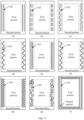
- FIG 8 shows a schematic sectional view of a groove in FIG 6 , namely, a schematic diagram of a shape of a section that is of the groove and that is in a plane where the thickness direction of the display panel is located.
- the shape of the section of the groove 1202 may be a rectangle (as shown in (a) of FIG 8 ), a triangle (as shown in (b) of FIG 8 ), a trapezoid (as shown in (c) of FIG 8 ), a parallelogram (as shown in (d) of FIG 8 ), a polyline (as shown in (e) of FIG 8 ), a wave (as shown in (f) of FIG 8 ), an ellipse (as shown in (g) of FIG 8 ), a flashlight (as shown in (h) of FIG 8 ), a stair, an arc, another regular shape or irregular shape (as shown in (i) of FIG 8 ), or the like.
- FIG 9 shows a schematic top view of a groove in FIG 6 , namely, a schematic diagram of a shape that is of the groove and that is in a plane where the display panel is located.
- the shape that is of the groove 1202 and that is in the plane where the display panel is located may be a straight line (as shown in (a), (b), and (c) of FIG 9 ), a curve (as shown in (d), (e), and (f) of FIG 9 ), a ring (as shown in (g), (h), and (i) of FIG 9 ), another regular shape or irregular shape, or the like.
- the shape that is of the groove and that is in the plane where the display panel is located in this embodiment of this application may be understood as an extending trend or extending direction of the groove in the plane.
- the shape of the section that is of the groove and that is in the plane where the thickness direction of the display panel is located is not limited herein.
- the shape of the section of the groove may be any of the shapes shown in FIG 8 .
- the shape that is of the groove 1202 and that is in the plane where the display panel is located is a straight line. This may also be understood as that the groove 1202 extends in the plane along the straight line.
- a bold line in the second portion of the array structure layer shown in (a) of FIG 9 is a schematic diagram of the extending direction of the groove 1202.
- the groove 1202 may be a long groove whose length is approximately equal to that of the first portion.
- the groove 1202 extends in a length direction of the first portion, and extends from one end to the other end of the first portion in the length direction.
- the groove 1202 is a solid-line groove in the length direction of the first portion.
- the groove 1202 may be a long groove whose width is approximately equal to that of the first portion; or the groove 1202 may be a solid-line groove in a width direction of the first portion. In other words, the groove 1202 may also be a solid-line groove extending in an edge direction of the first portion.
- the groove 1202 may extend along an edge of the first portion of the array structure layer, where the groove 1202 is a continuous groove in the extending direction.
- the second portion of the array structure layer may be provided with one or more solid-line grooves.
- the plurality of solid-line grooves may be arranged in parallel or crosswise.
- a shape of the solid-line grooves is simple, and a machining process of a mask plate used for fabricating the solid-line grooves is simple, so that the grooves can be obtained according to a process obtained by slightly changing an existing fabrication process of a display panel to pattern the array structure layer; and the grooves are filled with the organic material.
- the length of the groove 1202 is approximately equal to that of the first portion, so that the array structure layer may be filled with a relatively large quantity of organic materials, thereby effectively alleviating a problem of stress concentration on an edge of the array structure layer.
- a bold line in the second portion shown in (b) and (c) of FIG 9 is a schematic diagram of the groove 1202.
- the groove 1202 includes a plurality of sub-grooves in the edge direction of the first portion (for example, the length direction or width direction of the first portion), and a tail of a sub-groove is adjacent to but does not communicate with a head of a next sub-groove.
- the groove 1202 is a dashed-line groove extending in the edge direction of the first portion.
- the groove 1202 may extend along an edge of the first portion of the array structure layer.
- the groove 1202 is a groove that is intermittent in the extending direction, and may also be referred to as an intermittent groove.
- the array structure layer can be filled with the organic material uniformly, so that a problem of stress concentration on an edge of the array structure layer can be effectively alleviated.
- the second portion of the array structure layer may be provided with one or more dashed-line grooves.
- the plurality of dashed-line grooves may be arranged in parallel.
- one of two adjacent dashed-line grooves is referred to as a first dashed-line groove, and the other one is referred to as a second dashed-line groove.
- projections, in a direction perpendicular to an edge of the first portion, of a plurality of sub-grooves included in the first dashed-line groove and a plurality of sub-grooves included in the second dashed-line groove may completely overlap, for example, as shown in (b) of FIG 9 .
- the projections, in the direction perpendicular to the edge of the first portion, of the plurality of sub-grooves included in the first dashed-line groove and the plurality of sub-grooves included in the second dashed-line groove may partially overlap, that is, the plurality of sub-grooves included in the first dashed-line groove and the plurality of sub-grooves included in the second dashed-line groove are arranged alternately in the direction perpendicular to the edge of the first portion, for example, as shown in (c) of FIG 9 .
- the plurality of dashed-line grooves may be arranged crosswise.
- the sub-grooves included in the first dashed-line groove may not communicate with the sub-grooves included in the second dashed-line groove; or a first sub-groove in the first dashed-line groove communicates with a second sub-groove in the second dashed-line groove. This is not limited in this embodiment of this application.
- the array structure layer can be filled with the organic material more uniformly, so that a problem of stress concentration on an edge of the array structure layer can be effectively alleviated.
- the shape that is of the groove 1202 and that is in the plane where the display panel is located is a curve. This may also be understood as that the groove extends in the plane along the curve.
- a bold line in the second portion shown in each of (d) to (f) of FIG 9 is a schematic diagram of the groove 1202.
- the groove 1202 extends in the edge direction of the first portion.
- the groove 1202 may be a continuous curved groove (similar to the solid-line groove) or an intermittent curved groove (similar to the dashed-line groove) in the extending direction.
- the second portion of the array structure layer may be provided with one or more curved grooves.
- a distance between a point (hereinafter referred to as a farthest point) that is on the curved groove and that is farthest from the edge of the first portion and a point (hereinafter referred to as a closest point) that is on the curved groove and that is closest to the edge of the first portion may be slightly smaller than a width of the second portion in this direction.
- the distance between the farthest point and the closest point on the curved groove is less than or equal to 80% of the width of the second portion in this direction.
- the edge of the first portion is an outer edge of the first portion, namely, an edge of the display panel.
- the plurality of curved grooves may be arranged in parallel, for example, as shown in (e) of FIG 9 .
- parallel arrangement of the curved grooves herein may be understood as follows: In the direction perpendicular to the edge of the first portion, tangents of positions that correspond to every two curved grooves and that are in a same direction are parallel to each other.
- the plurality of curved grooves may be arranged crosswise, for example, as shown in (f) of FIG. 9 .
- one of two crosswise curved grooves is referred to as a first curved groove
- the other one is referred to as a second curved groove.
- the first curved groove and the second curved groove communicate at an intersection point, and do not communicate at a non-intersection point.
- the first curved groove and the second curved groove look like a fried dough twist as a whole.
- the first curved groove and the second curved groove may also be considered as two groove portions of one curved groove. This is not limited in this embodiment of this application.
- An extension form of the curved groove may be a wave, for example, a sine wave or a cosine wave.
- the array structure layer Due to arrangement of the curved groove in the array structure layer, the array structure layer can be filled with a relatively large quantity of organic materials, so that a problem of stress concentration on an edge of the array structure layer can be effectively alleviated.
- the curved groove is also relatively easy to machine, so that costs are relatively low.
- the shape that is of the groove 1202 and that is in the plane where the display panel is located is a ring. This may also be understood as that a head and an end of the groove 1202 are connected to or communicate with each other as a ring.
- the ring-shaped groove may be a circular ring-shaped groove, an elliptical ring-shaped groove, a square ring-shaped groove, a ring-shaped groove of another regular or irregular shape, or the like.
- the second portion of the array structure layer may be provided with a plurality of ring-shaped grooves.
- the plurality of ring-shaped grooves may be arranged on the array structure layer in the edge direction of the first portion regularly, for example, as shown in (g) of FIG 9 ; or the grooves may be arranged irregularly, for example, as shown in (h) of FIG 9 . This is not limited in this embodiment of this application. Shapes of the plurality of ring-shaped grooves may be the same or different.
- the ring-shaped groove may extend in the edge direction of the first portion, for example, as shown in (i) of FIG 9 .
- the groove may include a plurality of dents that are formed in the array structure layer and that do not communicate with each other.
- the plurality of dents may be arranged regularly or irregularly. This is not limited in this embodiment of this application.
- the non-display region of the display screen is disposed around the display region.
- the second portion of the array structure layer surrounds the first portion of the array structure layer.
- the groove may be disposed in some or all regions of the second portion.
- the display screen is a rectangle.
- the groove may be disposed in a region that is of the second portion and that is on a length side of the rectangle, for example, as shown in (a) to (h) of FIG 9 .
- the array structure layer has a bending deformation on the length side, thereby being prone to crack.
- the groove is disposed in a portion that cracks frequently, and is filled with the organic material, so that stress concentration of this portion can be effectively alleviated, and cracks can be reduced or avoided. Therefore, a dark dot problem is alleviated.
- the groove may alternatively be disposed around the first portion, for example, as shown in (i) of FIG 9 .
- all portions that are of the array structure layer and that have a relatively thick inorganic layer are filled with the organic material, thereby better alleviating a dark dot problem.
- first portion and the second portion in FIG 9 are merely exemplary. In practical application, for different electronic devices, the first portion and the second portion may have different arrangements. This is not limited in this embodiment of this application.
- a shape, a position, and the like of the groove in FIG 9 are merely exemplary. Those skilled in the art may design the groove according to actual needs. This is not particularly limited in this embodiment of this application.
- the above describes the shape of the groove from two aspects separately: the shape of the section of the groove and the extending trend of the groove in the second portion. If the shape of the groove is described from a three-dimensional perspective, the features in the foregoing two aspects may be included.
- the groove 1202 shown in FIG 6 may be a rectangular straight groove, a trapezoidal straight groove, a rectangular curved groove, a trapezoidal curved groove, a rectangular ring-shaped groove, a trapezoidal ring-shaped groove, or the like, which are merely described herein for illustration and are not listed one by one.
- a width of a groove and an interval between grooves may be designed according to actual needs.
- a width of the groove may range from 15 microns ( ⁇ m) to 25 microns ( ⁇ m).
- the width of the groove may be 15 ⁇ m, 18 ⁇ m, 20 ⁇ m, 23 ⁇ m, 25 ⁇ m, or the like.
- the groove may have equal or unequal widths in a depth direction.
- the widths are uniform in the depth direction.
- the widths are different in the depth direction.
- an average width of the groove in the depth direction may be considered as the width of the groove, or a maximum width of the groove in the depth direction may be considered as the width of the groove. This depends on the shape of the groove.
- an average value of radial dimensions of the groove may be considered as the width of the groove.
- an interval between grooves may range from 20 ⁇ m to 25 ⁇ m.
- the interval between the grooves may be 20 ⁇ m, 22 ⁇ m, 23 ⁇ m, 25 ⁇ m, or the like. It should be noted that an interval between grooves in the embodiments of this application may be understood as a shortest distance between two adjacent grooves.
- the groove may include a plurality of parallel trenches.
- the plurality of trenches extend along the edge of the first portion.
- a distance between two adjacent trenches in the plurality of trenches ranges from 20 microns to 25 microns.
- An appropriate distance between grooves can meet both the packaging performance requirement and the stress improvement capability requirement for the array structure layer.
- a width of a trench in the plurality of trenches that is close to the edge of the first portion is greater than or equal to a width of a trench in the plurality of trenches that is close to an edge of the display panel.
- the following describes an arrangement of the plurality of solid-line grooves by using an example in which the second portion of the array structure layer is provided with a plurality of parallel solid-line grooves and the plurality of solid-line grooves extend in the edge direction of the first portion, for example, as shown in (a) of FIG 9 .
- widths of the plurality of solid-line grooves may have a same value, for example, a1.
- Intervals between any two adjacent solid-line grooves in the plurality of solid-line grooves may have a same value, for example, b1.
- the widths of the plurality of solid-line grooves may alternatively be different.
- a width of a solid-line groove in the plurality of solid-line grooves that is close to the first portion may be greater than widths of the other solid-line grooves.
- the width of the solid-line groove close to the first portion is a2
- the widths of the other solid-line grooves are all a1, and a2 is greater than a1.
- the solid-line groove close to the first portion has a relatively large width, so that the solid-line groove may be filled with a large quantity of organic materials, which can effectively alleviate stress concentration in this region, and effectively prevent a crack from expanding to the first region and affecting display performance.
- the plurality of solid-line grooves may include solid-line grooves that are arranged alternately and that have different widths.
- a width of a relatively narrow solid-line groove is a1
- a width of a relatively wide solid-line groove is a2
- the two solid-line grooves are arranged alternately in a direction perpendicular to the edge of the first portion.
- intervals between any two adjacent solid-line grooves in the plurality of solid-line grooves may alternatively be different.
- an interval of two solid-line grooves that are in the plurality of solid-line grooves and that are close to the first portion may be greater than intervals between two adjacent solid-line grooves in the other solid-line grooves.
- the interval between the two solid-line grooves close to the first portion is b2
- the intervals between two adjacent solid-line grooves in the other solid-line grooves are all b1, and b2 is greater than b1.
- a relatively thick inorganic layer is superimposed on a position that is of the array structure layer and that is close to an edge, that is, an edge region of the second portion is more prone to crack.
- a groove having relatively high density is disposed in this region, so that the inorganic layer in this region may be filled with a larger quantity of organic materials. Therefore, stress concentration in this region can be effectively alleviated, and crack expansion can be effectively prevented.
- grooves are a plurality of dashed-line grooves or a plurality of curved grooves, a similar arrangement is used. Details are not described again.
- a shortest distance between the groove and the edge of the display panel ranges from 200 microns to 250 microns.
- a distance between a trench at a position close to the edge of the array structure layer and the edge of the array structure layer may range from 200 ⁇ m to 250 ⁇ m. Since the inorganic layer of the second portion of the array structure layer is mainly used to complete packaging, that is, to prevent intrusion of water and oxygen, there is a sufficient distance between an outermost side of the groove and the edge of the display panel. Therefore, the inorganic layer on the edge of the array structure layer has a sufficient width to ensure packaging performance.
- the distance between the trench and the edge of the array structure layer (which may be understood as the edge of the display panel) may be understood as a distance between the edge of the array structure layer and a point that is of the trench and that is closest to the edge.
- a depth of the groove is less than or equal to a thickness of the array structure layer, that is, the groove may partially or completely penetrate the array structure layer.
- the depth of the groove is greater than or equal to one second of the thickness of the array structure layer.
- the second portion of the array structure layer may be filled with a relatively large quantity of organic materials, to alleviate a stress concentration problem of the second portion.
- the array structure layer (namely, the BP inorganic layer) in the non-display region of the display panel is patterned and is filled with an organic matter, so that stress concentration of the BP inorganic layer can be alleviated, crack expansion can be prevented, and a problem that an inorganic layer at a packaging position on an edge of the display panel cracks can be alleviated effectively. Therefore, a GDS-type dark dot problem caused by cracking of the BP inorganic layer is alleviated, thereby prolonging a service life of the display panel, and improving user's experience.
- FIG 11 shows a schematic sectional view of another OLED display panel according to an embodiment of this application.
- the display panel 300 includes a base 11, an array structure layer 12, an organic planarization layer 16, a light-emitting component layer 13, and a packaging layer 14.
- the base 11 is a matrix for forming another film layer and mainly plays roles in supporting and sealed packaging.
- the array structure layer 12 is disposed on the base 11 and is configured to form a drive circuit 1201 that drives the light-emitting component layer 13 to emit light.
- the array structure layer 12 includes a first portion and a second portion.
- the first portion is a projection portion of the display region on the array structure layer 12.
- the second portion is a projection portion of the non-display region on the array structure layer 12.
- the drive circuit 1201 includes a thin-film transistor layer that is disposed on the first portion of the array structure layer 12.
- the thin-film transistor layer includes a plurality of thin-film transistors. Each of the plurality of thin-film transistors is configured to control, to be on/off, a display unit that is on the light-emitting component layer 13 and that corresponds to the thin-film transistor.
- the second portion of the array structure layer 12 is provided with the groove 1202.
- the organic planarization (planarization, PLN) layer 16 is disposed on the array structure layer 12 and is configured to provide a planarized surface for the light-emitting component layer 13 to facilitate light extraction.
- the organic planarization layer 16 covers the first portion of the array structure layer 12.
- the groove 1202 is filled with a first organic material.
- the organic planarization layer 16 includes the first organic material.
- the organic planarization layer 16 includes an organic material covering the first portion and an organic material (namely, the first organic material) filled in the groove 1202.
- the first organic material is the same as a material of the organic planarization layer 16.
- the light-emitting component layer 13 is disposed on the organic planarization layer 16 and is configured to form a display unit for displaying an image.
- the packaging layer 14 is disposed on the light-emitting component layer 13, covers the light-emitting component layer 13, and extends to the second portion of the array structure layer 12.
- the packaging layer 14 covers the second portion of the array structure layer 12 and covers the first organic material filled in the groove 1202.
- the packaging layer 14 mainly plays a role in packaging to prevent intrusion of water and oxygen.
- the filling layer 15 of the display panel 200 may be a film layer separately disposed for filling the groove 1202, and that the display panel 300 may include the organic planarization layer 16 for providing a planarized surface. Therefore, in the display panel 300, the organic planarization layer 16 may be used to fill the groove 1202. In this way, the first organic material filled in the groove 1202 is equivalent to the filling layer 15 in the display panel 200.
- Functions of the film layers, an arrangement of the groove 1202, and the like in the display panel 300 are similar to those in the display panel 200. For detailed, refer to the foregoing descriptions. For brevity, details are not described herein again.
- the groove is fabricated in the non-display region of the display panel and is filled with an existing organic film layer such as a planarization layer.
- the array structure layer can be filled with the organic material according to a simple fabrication process obtained by slightly changing an existing fabrication process of a display panel, thereby alleviating the dark dot problem.
- the display panel further includes a signal cable layer located on the array structure layer.
- the signal cable layer is provided with a signal cable on the second portion of the array structure layer.
- the groove disposed on the second portion corresponds to a position of the signal cable.
- a relatively thick inorganic layer is superimposed under the signal cable in the non-display region. Therefore, a groove may be disposed in a film layer under the signal cable in the non-display region, and filled with an organic matter. This can alleviate stress concentration of the BP inorganic layer, prevent crack expansion, effectively alleviate the dark dot problem, and prolong a service life of the display panel.
- the signal cable may include a voltage of source series (voltage of source series, VSS) signal cable.
- VSS voltage of source series
- the second portion of the array structure layer includes an insulation layer, a buffer layer, a gate insulation layer, and an inter-layer dielectric layer that are stacked in sequence. All of the insulation layer, the buffer layer, the gate insulation layer, and the inter-layer dielectric layer are inorganic film layers.
- the following describes some specific non-restrictive examples of the embodiments of this application in more detail. It should be understood that the following embodiments merely illustrate a display panel structure that alleviates the dark dot problem in the foregoing manner of disposing a groove and filling the groove with an organic matter. However, the foregoing structure for alleviating the dark dot problem is also applicable to other display panels. Details are not described herein one by one.
- FIG 12 shows a schematic top view of a display panel according to an embodiment of this application.
- the display panel 400 includes a display region and a non-display region extending around the display region.
- the display region is provided with a display unit, used for displaying an image.
- the display region may also be referred to as a pixel area, a pixel light-emitting area, or an array area (array area, AA).
- the non-display region sequentially includes a gate on array (gate on array, GOA) area, a voltage of source series (voltage of source series, VSS) area, an ink jet printing (ink jet printing, IJP) dam (dam) area, a crack (crack) barrier area, and a heat-affected area.
- GOA gate on array
- VSS voltage of source series
- IJP ink jet printing
- dam crack
- Crack crack
- the GOA area is used to provide a row driver for an array substrate, that is, provide a driver for a TFT that controls the display unit to be on/off.
- the array substrate may be understood as a structure obtained after an array structure layer is formed on a base.
- the array substrate includes a drive circuit and the base.
- the VSS area is used to provide a source voltage. Specifically, the VSS area is used to provide a voltage for a cathode (for example, the cathode 1015 in FIG 3 ) in an OLED display panel.
- a cathode for example, the cathode 1015 in FIG 3
- the IJP dam area is used to prevent an ink jet printing layer applied on the display panel from overflowing, thereby achieving a better edge packaging effect.
- the crack barrier area is used to prevent a cutting crack from expanding to the display region during cutting of the display panel, resulting in intrusion of water and oxygen.
- the heat-affected area is an area reserved for a cutting process of the display panel. If a crack is generated in the cutting process, the heat-affected area can block the cutting crack.
- FIG. 12 and subsequent drawings only schematically show approximate positions of the areas, and there are no strict boundaries between the areas.
- FIG 13 shows a schematic sectional view of an OLED display panel according to an embodiment of this application.
- FIG 13 may be a schematic sectional view along a line B-B of the display panel in FIG 12 .
- the base 11 may include a first substrate 111, a barrier 112, and a second substrate 113 that are stacked.
- the barrier 112 is located between the first substrate 111 and the second substrate 113, and is attached to each of the first substrate 111 and the second substrate 113.
- the first substrate 111 and the second substrate 113 are bases used for fabricating the display panel. Subsequently, fabrication of a thin-film transistor TFT, evaporation, packaging, and the like are all performed on the bases.
- the first substrate 111 and the second substrate 113 may be glass substrates. In this case, the display panel is a hard display panel.
- the first substrate 111 and the second substrate 113 may be polyimide (polyimide, PI) substrates (substrates). In this case, the display panel is a flexible display panel.
- Polyimide PI is a flexible plastic material with high tensile strength, bending strength and compressive strength, and has outstanding creep resistance and dimensional stability. Like glass, polyimide PI may be stacked with organic layers on a TFT and PI. An initial state of polyimide PI is liquid. To be used as a base for fabricating a display panel, a PI material may be first applied on a glass base referred to as carrier glass, and is then cured for formation.
- the barrier (barrier) 112 is used to isolate the first substrate 111 from the second substrate 113, and can also play a role in isolating sodium ions and potassium ions in the carrier glass.
- the barrier 112 may be a silica (SiO 2 ) film layer.
- the barrier 112 may alternatively be a silicon nitride (SiNx) film layer.
- the base 11 includes two substrates that can enhance strength of the base 11.
- the base 11 may include one substrate or more than two substrates.
- a structure of the base 11 may vary correspondingly. Specifically, the structure may be flexibly designed according to actual needs, which is not particularly limited herein.
- first substrate 111 and the second substrate 113 may alternatively be made of another flexible material, which is not limited in this embodiment of this application.
- the base 11 may further include another film layer, for example, an amorphous silicon (a-Si) protective film layer that is used to absorb laser lift off (laser lift off, LLO) energy during peeling off of the display panel, thereby preventing damage to a TFT layer.
- a-Si amorphous silicon
- the protective film layer may be disposed between the first substrate 111 and the second substrate 113, for example, the protective film layer is disposed on the barrier 112 and covers the barrier 112.
- the array structure layer 12 is disposed on the base 11 and may include an insulation layer 121, a buffer layer 122, a TFT layer 123, a storage capacitor 124, a gate insulation layer 125, and an inter-layer dielectric layer 126.
- the insulation layer 121 is disposed on the second substrate 113 and covers the second substrate 113.
- the insulation layer 121 is used to isolate the base 11 from the TFT layer 123, and can play a role in isolating sodium ions and potassium ions in the carrier glass.
- the buffer (buffer) layer 122 is disposed on the insulation layer 121, covers the insulation layer 121, and can play roles in buffering and heat preservation.
- the buffer layer 122 may be a composite film layer, for example, a composite film layer of silicon nitride (SiNx) and silica (SiO 2 ), which can play a role in heat preservation in a subsequent annealing process.
- the TFT layer 123 mainly includes an active layer 1231, a gate 1232, and a source/drain.
- the storage capacitor 124 mainly includes a first electrode 1241 and a second electrode 1242.
- the gate insulation (gate insulation, GI) layer 125 includes a first gate insulation layer 1251 and a second gate insulation layer 1252 that are stacked.
- the active layer 1231 is disposed on the buffer layer 122 and used to form a conducting channel.
- the active layer 1231 may be made of amorphous silicon (a-Si) or poly-silicon (poly-silicon, p-Si), where the poly-silicon may be low temperature poly-silicon (low temperature poly-silicon, LTPS).
- a thin-film transistor using an LTPS technology may also be referred to as an LTPS TFT, which has high electron mobility, a small area of a thin-film circuit, a simple structure, and high stability.
- the material of the active layer 1231 may alternatively be a metal oxide, for example, indium gallium zinc oxide (indium gallium zinc oxide, IGZO) or the like.
- the first gate insulation layer 1251 is disposed on the active layer 1231, covers the active layer 1231, and extends to the buffer layer 122. In some embodiments, the first gate insulation layer 1251 covers the active layer 1231 and the buffer layer 122. The first gate insulation layer 1251 is located between the gate 1232 and the active layer 1231, and is used to isolate the active layer 1231 from the gate 1232, thereby preventing conduction between the gate 1232 and the active layer 1231, and playing roles in insulation and static prevention.
- the first gate insulation layer 1251 is made of an insulating material, for example, silica (silica) SiO 2 , a composite stacked layer of SiO 2 and SiNx, or the like.
- the gate 1232 and the first electrode 1241 are disposed on the first gate insulation layer 1251.
- the gate 1232 is disposed adjacent to the first electrode 1241 without conduction.
- the gate 1232 is a gate of the thin-film transistor TFT.
- the gate is connected to a row electrode (which is not shown in the figure and may be learned through reference to the row electrode 1017 in FIG 4 ), and is used to control conduction of a TFT channel, thereby controlling the display unit to be on/off.
- the gate 1232 is located above the active layer 1231.
- the gate 1232 is a conductor made of metal chromium (Cr), an alloy material of chromium, a molybdenum-tantalum (MoTa) alloy, aluminum (Al), molybdenum (Mo), copper (Cu), or another conductor with high electrical conductivity.
- the first electrode 1241 is one of electrodes of the storage capacitor (storage capacitor, Cst) 124, is connected to a column electrode (not shown in the figure), and is used to charge the storage capacitor 124.
- the storage capacitor is used to maintain current, thereby driving the display panel.
- the first electrode 1241 and the gate 1232 may be fabricated in a same fabrication process, and may also be fabricated by using a same mask plate. In other words, the gate 1232 and the first electrode 1241 may be considered as being located on a same film layer without mutual conduction.
- the first electrode 1241 may be made of the same material as the gate 1232, for example, metal chromium (Cr), an alloy material of chromium, a molybdenum-tantalum (MoTa) alloy, aluminum (Al), molybdenum (Mo), copper (Cu), or another conductor with high electrical conductivity.
- metal chromium Cr
- an alloy material of chromium a molybdenum-tantalum (MoTa) alloy
- Al aluminum
- Mo molybdenum
- Cu copper
- the second gate insulation layer 1252 is disposed on the gate 1232 and the first electrode 1241, covers the gate 1232 and the first electrode 1241, and extends to the first gate insulation layer 1251. In some embodiments, the second gate insulation layer 1252 covers the gate 1232, the first electrode 1241, and the first gate insulation layer 1251.
- the second gate insulation layer 1252 serves as an insulation layer between storage capacitors, which is equivalent to a capacitor dielectric layer, to prevent conduction between the first electrode 1241 and the second electrode 1242, so that the first electrode 1241 and the second electrode 1242 form a storage capacitor Cst.
- the second gate insulation layer 1252 is made of an insulating material, for example, silicon nitride (silicon nitride) SiNx.
- the second electrode 1242 is disposed on the second gate insulation layer 1252, located above the first electrode 1241, and opposite the first electrode 1241.
- the second electrode 1242 is another electrode of the storage capacitor 124, and is connected to the gate of the thin-film transistor that drives the display unit to emit light.
- the first electrode 1241 and the second electrode 1242 may provide a stable switch-on voltage to the thin-film transistor that drives the display unit to emit light.
- a structure shown in FIG 13 is used as an example.
- the first electrode 1241 and the second electrode 1242 are arranged opposite each other.
- the first electrode 1241 may be referred to as a lower electrode of the storage capacitor 124
- the second electrode 1242 may be referred to as an upper electrode of the storage capacitor 124.
- the second electrode 1242 may be made of the same material as the first electrode 1241. For details, refer to the foregoing descriptions. Details are not described again.
- the inter-layer dielectric (inter layer dielectric, ILD) layer 126 is disposed on the second electrode 1242, covers the second electrode 1242, and extends to the second gate insulation layer 1252.
- the inter-layer dielectric layer 126 is used to isolate the gate 1232 from the column electrode (which may also be referred to as SD metal), and may provide hydrogen atoms (H atoms) for a poly-silicon conducting channel in the active layer 1231 to fill a defect.
- the inter-layer dielectric layer 126 is a composite film layer, for example, including a first inter-layer dielectric layer 1261 and a second inter-layer dielectric layer 1262 that are stacked.
- the first inter-layer dielectric layer 1261 is located on a side close to the second electrode 1242.
- the second inter-layer dielectric layer 1262 is located on a side away from the second electrode 1242.
- the first inter-layer dielectric layer 1261 and the second inter-layer dielectric layer 1262 are made of different insulating materials.
- the first inter-layer dielectric layer 1261 may be made of silica SiO 2
- the second inter-layer dielectric layer 1262 may be made of silicon nitride SiNx.
- the source/drain (source/drain, S/D) in the TFT may include a first source/drain portion 1233 and a second source/drain portion 1234.
- the first source/drain portion 1233 is disposed on the inter-layer dielectric layer 126, passes through all film layers between the active layer 1231 and the first source/drain portion 1233, and is connected to the active layer 1231.
- a film layer for example, the inter-layer dielectric layer 126 or the gate insulation layer 125, between the active layer 1231 and the first source/drain portion 1233 may be provided with a first hole 1203.
- the first source/drain portion 1233 is disposed on the inter-layer dielectric layer 126 and filled in the first hole 1203, thereby implementing contact with the active layer 1231.
- the first source/drain portion 1233 includes a source (source, S) and a drain (drain, D).
- the source S and the drain D are separated from each other and each are in contact with the active layer 1231, so that part of the active layer 1231 leaks out from a space between the source S and the drain D.
- the gate 1232 is located between the source S and the drain D and is not in contact with the source S and the drain D.
- the source S is connected to the column electrode.
- the drain D is connected to the anode 131 of the display unit through the second source/drain portion 1234, and is used to control luminance of the display unit. A position of the second source/drain portion 1234 is described below in detail. Details are not described herein.
- a relatively thick inorganic layer is superimposed on the base 11.
- the insulation layer 121, the buffer layer 122, the gate insulation layer 125, and the inter-layer dielectric layer 126 are stacked in sequence. Therefore, a relatively thick BP inorganic layer (including the insulation layer 121, the buffer layer 122, the gate insulation layer 125, and the inter-layer dielectric layer 126) is superimposed on the non-display region of the display panel, for example, the VSS area, and has a relatively high elastic modulus.
- the inorganic layer in the non-display region is prone to crack, which easily causes intrusion of water and oxygen, and results in a dark dot problem.
- a groove 1202 is disposed in a region that is of the non-display region and where the inorganic layer is superimposed; and the groove 1202 is filled with the filling layer 15 (or the first organic material described above).
- a material of the filling layer 15 is an organic material, for example, polyimide, polytetrafluoroethylene, acrylic resin, polyethylene, polyvinyl chloride, polypropylene, phenolic resin, epoxy resin, polybutadiene, polyisoprene, chloroprene rubber, butyl rubber, or the like.
- the groove is fabricated by patterning a region that is of the non-display region and that has a relatively thick inorganic layer (for example, the BP inorganic layer in the VSS area), and is filled with an organic matter, thereby playing roles in buffering stress on this region and preventing crack expansion.
- a relatively thick inorganic layer for example, the BP inorganic layer in the VSS area
- An elastic modulus of the material of the filling layer 15 may range from 2 gigapascals (GPa) to 5 GPa, and transmittance of visible light may be 95% ⁇ 3%.
- the groove 1202 in the non-display region may be fabricated in the same process as the first hole 1203 in the display region, or fabricated after fabrication of the inter-layer dielectric layer 126 and before fabrication of the first hole 1203, or fabricated in a process next to fabrication of the first hole 1203, which is not limited in this embodiment of this application.
- a depth of the groove 1202 may be flexibly designed according to actual needs.
- the groove 1202 may penetrate the inter-layer dielectric layer 126, the gate insulation layer 125, the buffer layer 122, and the insulation layer 121; or the depth of the groove 1202 may be less than the sum of depths of the inter-layer dielectric layer 126, the gate insulation layer 125, the buffer layer 122, and the insulation layer 121; or the depth of the groove 1202 may be equal to a depth of the first hole 1203.
- the filling layer 15 may be filled in the groove 1202 in a separate process, for example, filled in the groove 1202 before deposition of the first source/drain portion 1233, or filled in the groove 1202 in a process after deposition of the first source/drain portion 1233, or filled in the groove 1202 in any process before fabrication of a film layer capable of covering the groove 1202.
- the filling layer 15 may be fabricated in a subsequent process of fabricating an organic film layer, that is, the filling layer 15 and the organic film layer are made of the same material and are fabricated in the same process.
- the first planarization layer 161 is fabricated after fabrication of the first source/drain portion 1233.
- the first planarization layer 161 is disposed on the first source/drain portion 1233, covers the first source/drain portion 1233, and extends to the inter-layer dielectric layer 126.
- the groove 1202 is filled with the first planarization layer 161 to form the foregoing filling layer 15, namely, the first organic material.
- the first planarization layer 161 covers a region that is of the inter-layer dielectric layer 126 and that corresponds to an AA region, and is filled in the groove 1202.
- a side surface, away from the base 11, of the first planarization layer 161 (namely, the filling layer 15 or the first organic material) in the groove 1202 is flush with a side surface, away from the base 11, of the inter-layer dielectric layer 126.
- a gate on array (gate on array, GOA) 171 and an emission on array (emission on array, EOA) 172 may also be disposed on the inter-layer dielectric layer 126 before, after, or during fabrication of the first source/drain portion 1233.
- the gate on array 171 is configured to provide a row driver for an array substrate.
- the emission on array 172 is configured to provide an emission driver for the array substrate.
- the TFT controls the display unit to be on/off, but the gate on array 171 and the emission on array 172 jointly control the TFT to be on/off. Therefore, multi-level control is realized.
- the gate on array 171 and the emission on array 172 are not electrically connected to the source/drain of the TFT layer 123.
- positions of the gate on array 171 and the emission on array 172 in FIG 13 are merely exemplary, and may be designed flexibly by those skilled in the art according to actual needs.
- there may alternatively be no emission on array 172 that is, the gate on array 171 can directly control the TFT to be on/off.
- a region where the gate on array 171 and the emission on array 172 are located may be considered as the GOA area described above.
- the GOA area is located at a periphery of the AA region and is disposed around the AA region.
- the gate on array 171 and the emission on array 172 may be fabricated before or after fabrication of the first planarization layer 161, which is not limited in this embodiment of this application.
- the second source/drain portion 1234 described above is disposed on the first planarization layer 161, passes through a second hole 1204 disposed on the first planarization layer 161, and is in contact with the first source/drain portion 1233.
- the display panel 300 further includes a light-emitting component layer 13 disposed on the array structure layer 12.
- the light-emitting component layer 13 includes an anode 131, a hole transport layer (which is not shown in the figure and may be learned through reference to the hole transport layer 1012 in FIG 3 ), an organic light-emitting layer 132, an electron transport layer (which is not shown in the figure and may be learned through reference to the electron transport layer 1014 in FIG 3 ), and a cathode 133.
- a voltage of the anode 131 is provided by the source/drain of the TFT layer 123.
- a voltage of the cathode 133 is provided by the voltage of source series VSS 18.
- the voltage of source series 18 includes a first signal cable portion 181 and a second signal cable portion 182.
- the first signal cable portion 181 is disposed on the inter-layer dielectric layer 126 and covers the filling layer 15 filled in the groove 1202.
- the first signal cable portion 181 may be fabricated in the same process as the second source/drain portion 1234, the first signal cable portion 181 may be made of the same material as the second source/drain portion 1234.
- the first planarization layer 161 covers the region that is of the inter-layer dielectric layer 126 and that corresponds to the AA region, and is filled in the groove 1202
- the first signal cable portion 181 may cover part of a region that is of the inter-layer dielectric layer 126 and that corresponds to the non-display region, and covers the first planarization layer 161 filled in the groove 1202; and the second source/drain portion 1234 is disposed on the first planarization layer 161.
- the organic planarization layer 16 in this embodiment of this application further includes a second planarization layer 162.
- the second planarization layer 162 is disposed on the second source/drain portion 1234, covers the second source/drain portion 1234, and extends to the first planarization layer 161.
- the second planarization layer 162 may cover the second source/drain portion 1234 and the first planarization layer 161, and cover part of regions of the emission on array 172 and the gate on array 171.
- a third planarization layer 163 is also disposed on part of a region of the first signal cable portion 181 to provide the first signal cable portion 181 and the second signal cable portion 182 with relatively flat surfaces, thereby reducing impedance and ensuring that a light-emitting surface is flat.
- the third planarization layer 163 may be a film layer fabricated separately, for example, is fabricated before or after fabrication of the second planarization layer 162.
- the third planarization layer 163 may alternatively be fabricated in the same process as the second planarization layer 162. Therefore, it may be considered that the third planarization layer 163 is part of the second planarization layer 162 but has a different function. In this embodiment of this application, the third planarization layer 163 is separated from and does not communicate with the second planarization layer 162.
- the anode 131 is disposed on the second planarization layer 162, and is in contact with the second source/drain portion 1234 after passing through a third hole 1205 in the second planarization layer 162.
- the second source/drain portion 1234 is connected to the first source/drain portion 1233 and the anode 131, and can transmit a signal on the column electrode (namely, the data line) to the anode 131, thereby controlling luminance of the display unit.
- the second signal cable portion 182 is disposed on the third planarization layer 163, covers the third planarization layer 163, and extends to the first signal cable portion 181. In this way, the first signal cable portion 181 is electrically connected to the second signal cable portion 182.
- the second signal cable portion 182 is also in contact with the cathode 133, so that voltages provided by the first signal cable portion 181 and the second signal cable portion 182 may be provided for the cathode 133.
- a manner of a connection between the cathode 133 and the second signal cable portion 182 is described below in detail, and is not described herein.
- a pixel definition layer (pixel definition layer, PDL) 19 included in the display panel 300 is disposed on the anode 131, covers part of the anode 131, and extends to the second planarization layer 162. As shown in FIG 13 , the pixel definition layer 19 is provided with an opening 1206.
- the opening 1206 corresponds to a position of the anode 131, so that the anode 131 is exposed from the pixel definition layer 19.
- a region of the opening 1206 is a light-emitting region on the display panel.
- a pixel spacer (pixel spacer, PS) layer 134 is disposed on the pixel definition layer 19, and is used to support a mask plate used for evaporation of the organic light-emitting layer 132 and evaporation of the cathode.
- the mask plate is a fine metal mask (fine metal mask, FMM).
- the organic light-emitting layer 132 in the light-emitting component layer 13 is disposed on the anode 131 and located in the opening 1206.
- the organic light-emitting layer 132 can emit light after a voltage is applied between the anode 131 and the cathode 133.
- the opening 1206 may form a resonant cavity.
- a side wall of the opening 1206 can reflect light, thereby achieving higher light emitting efficiency.
- the cathode 133 is disposed on the organic light-emitting layer 132, covers the organic light-emitting layer 132, extends to the pixel definition layer 19 and the second signal cable portion 182, and is used to provide electrons for a light-emitting component. In this way, the voltage of source series may be provided for the cathode 133 through the first signal cable portion 181 and the second signal cable portion 182.
- a region where the first signal cable portion 181 and the second signal cable portion 182 are located may be considered as the VSS area described above.
- the active layer 1231 is disposed between the buffer layer 122 and the first gate insulation layer 1251; and the first gate insulation layer 1251 coats the active layer 1231 and extends to the buffer layer 122.
- the gate 1232 is disposed between the first gate insulation layer 1251 and the second gate insulation layer 1252; the second gate insulation layer 1252 coats the gate 1232 and extends to the first gate insulation layer 1251; and the gate 1232 is disposed opposite the active layer 1231.
- the first source/drain portion 1233 is disposed between the inter-layer dielectric layer 126 and the first planarization layer 161; the first planarization layer 161 coats the first source/drain portion 1233 and is filled in the groove 1202; and the first source/drain portion 1233 is connected to the active layer 1231 after sequentially penetrating the inter-layer dielectric layer 126, the second gate insulation layer 1252, and the first gate insulation layer 1251.
- the second source/drain portion 1234 is disposed between the first planarization layer 161 and the second planarization layer 162; the second planarization layer 162 coats the second source/drain portion 1234 and extends to the first planarization layer 161; and the second source/drain portion 1234 is connected to the first source/drain portion 1233 after penetrating the first planarization layer 161.
- a first signal cable portion 181 is disposed in a region, corresponding to the groove 1202, of the inter-layer dielectric layer 126.
- the first signal cable portion 181 is a signal cable fabricated on the same layer as the second source/drain portion 1234, and the first signal cable portion 181 covers the filling layer 15 (or referred to as the first organic material) filled in the groove 1202 and the inter-layer dielectric layer around the groove.
- the anode 131 is disposed on the second planarization layer 162, and is connected to the second source/drain portion 1234 after penetrating the second planarization layer 162.
- a second signal cable portion 182 is disposed on the first signal cable portion 181, is connected to the first signal cable portion 181, and is a signal cable fabricated on the same layer as the anode 131.
- the cathode 133 is disposed on the organic light-emitting layer 132, covers the organic light-emitting layer 132, and extends to the second signal cable portion 182.
- the first signal cable portion 182 and the second signal cable portion 182 are part of a voltage of source series VSS signal cable.
- An IJP dam area is disposed on a side, close to an edge of the display panel, of the VSS area.
- the IJP dam area is provided with one or more dams 144 used for preventing an ink jet printing layer in the packaging layer 14 from overflowing.
- the dam 144 may be disposed on the inter-layer dielectric layer 126 or disposed on the first signal cable portion 181, which is not limited in this embodiment of this application.
- the dam 144 may be fabricated after fabrication of the second source/drain portion 1234 and before fabrication of the packaging layer 14, for example, fabricated in a process after fabrication of the cathode 133 or fabricated in a process after fabrication of the first signal cable portion 181, which is not limited in this embodiment of this application.
- a crack barrier area is disposed on a side, close to the edge of the display panel, of the IJP dam area.
- the crack barrier area generally includes an inter-layer dielectric layer 126, a gate insulation layer 125, a buffer layer 122, an insulation layer 121, a base 11, and the like.
- the crack barrier area is provided with one or more trenches 145 used for preventing a cutting crack from expanding to the AA region.
- a heat-affected area is disposed on a side, close to the edge of the display panel, of the crack barrier area.
- the display panel 300 is a flexible display panel
- a packaging process of the display panel generally uses a thin-film encapsulation (thin-film encapsulation, TFE) process to prevent moisture and oxygen from entering the display panel.
- the display panel 300 includes the packaging layer 14 disposed on the light-emitting component layer 13.
- the packaging layer 14 includes an organic layer and an inorganic layer.
- the packaging layer 14 includes a first chemical vapor deposition layer 141, an ink jet printing layer 142, and a second chemical vapor deposition layer 143 that are stacked.
- the first chemical vapor deposition layer 141 is disposed on the cathode 133, covers the cathode 133, and extends to the second signal cable portion 182, the first signal cable portion 181, the dam 144, and the inter-layer dielectric layer 126.
- the ink jet printing layer 142 is disposed on the first chemical vapor deposition layer 141 and located in a region surrounded by the dam 144.
- the second chemical vapor deposition layer 143 is disposed on the inkjet printing layer 142, covers the ink jet printing layer 142, and extends to the first chemical vapor deposition layer 141.
- the first chemical vapor deposition layer 141 and the second chemical vapor deposition layer 143 are inorganic packaging layers used for preventing an electroluminescent component and the cathode from being intruded by water and oxygen.
- the ink jet printing layer 142 is configured to implement planarization and play a role in wrapping a foreign matter, thereby improving packaging performance.
- the VSS area that is of the display panel and that is prone to crack is structurally improved as follows: An inorganic layer below the VSS area on the edge of the display panel is patterned to fabricate the groove, and the groove is filled with an organic matter. This can alleviate stress concentration of the BP inorganic layer below the VSS area; prevent crack expansion; effectively alleviate a GDS-type dark dot problem that is in the VSS area on the edge of the display panel and that is caused by cracking of the BP inorganic layer; and prolong a service life of the display panel.
- the structure of the display panel 300 in this embodiment of this application is merely exemplary.
- the display panel may have another structural form, such as a TFT of another structural form or a driving structure of another form, provided that a groove can be disposed in the non-display region of the display panel and be filled with an organic matter. Therefore, cracks are reduced, expansion of a crack is prevented, and the dark dot problem is alleviated.
- the display panel is a flexible display panel is used as an example.
- Film layers of the display panel may be peeled off after being stacked on carrier glass.
- the carrier glass is cleaned before stacking, to prevent impurities from polluting the film layers and to facilitate applying the film layers with uniform thicknesses.
- Step 1 Form a base on the carrier glass.
- first substrate 111, the barrier 112, and the second substrate 113 may be sequentially formed on the carrier glass 104.
- Step 1-1 Form the first substrate 111 on the carrier glass.
- the first substrate 111 is made of a polyimide PI material.
- PI may be applied on the carrier glass and be cured, and then the first substrate 111 is formed.
- a thickness of the first substrate 111 may range from 8.5 ⁇ m to 10 ⁇ m; and an error of the thickness may be within 1 ⁇ m.
- Step 1-2 Form the barrier 112 on the first substrate 111.
- a chemical vapor deposition (chemical vapor deposition, CVD) technology for example, a plasma enhanced chemical vapor deposition (plasma enhanced chemical vapor deposition, PECVD) technology or a microwave plasma chemical vapor deposition (microwave plasma chemical vapor deposition, MPCVD) technology may be used to deposit the barrier 112 on the first substrate 111.
- CVD chemical vapor deposition
- PECVD plasma enhanced chemical vapor deposition
- MPCVD microwave plasma chemical vapor deposition
- the barrier 112 may be a SiO 2 film layer.
- a thickness of the barrier 112 may range from 550 nanometers (nm) to 750 nanometers (nm).
- Step 1-3 Form the second substrate 113 on the barrier 112.
- the second substrate 113 is made of a polyimide PI material.
- a thickness of the second substrate 113 and the thickness of the first substrate 111 may be the same, and may have the same error.
- the protective layer may absorb LLO energy subsequently, to play a role in preventing the LLO energy from damaging the thin-film transistor TFT.
- the protective layer may be formed on the barrier 112, that is, the protective layer is located between the barrier 112 and the second substrate 113.
- the protective layer may be an amorphous silicon (a-Si) film layer.
- a thickness of the protective layer may range from 4 nm to 5 nm.
- the first substrate 111, the barrier 112, and the second substrate 113 are all formed via full-side applying.
- FIG 15 Further reference is made to FIG 15 .
- Step 2 Form the array structure layer on the base.
- the insulation layer 121, the buffer layer 122, the active layer 1231, the first gate insulation layer 1251, the gate 1232, the first electrode 1241, the second gate insulation layer 1252, the second electrode 1242, the inter-layer dielectric layer 126, and the source/drain are sequentially formed on the base. Specific steps are as follows.
- Step 2-1 Form the insulation layer 121 on the second substrate 113.
- the insulation layer 121 may be fabricated in the same manner as the barrier 112 shown in FIG 14 .
- the PECVD technology is used to deposit the insulation layer 121 on the second substrate 113.
- the insulation layer 121 may be a SiO 2 film layer.
- a thickness of the insulation layer 121 may range from 550 nm to 750 nm.
- the barrier 112 shown in FIG 14 and the insulation layer 121 shown in FIG 15 may be both considered to play a role in isolating a substrate (for example, the first substrate 111 or the second substrate 113) in the base from another film layer, may both play a role in isolating metal ions such as potassium ions and sodium ions in the carrier glass, and may further function as the buffer layer.
- Step 2-2 Form the buffer layer 122 on the insulation layer 121.
- the buffer layer 122 may be deposited on the insulation layer 121 by using the PECVD technology.
- the buffer layer 122 may be a single film layer or a composite film layer.
- the buffer layer 122 can play a role in heat preservation in a subsequent process such as an excimer laser annealing (excimer laser annealing, ELA) process.
- ELA excimer laser annealing
- the buffer layer 122 is a composite film layer of a SiNx film layer and a SiO 2 film layer.
- a thickness of the SiNx film layer may range from 180 nm to 250 nm.
- a thickness of the SiO 2 film layer may range from 300 nm to 350 nm.
- Step 2-3 Form the active layer 1231 of the TFT on the buffer layer 122.
- the active layer 1231 may be an amorphous silicon layer, a poly-silicon layer, or a metal oxide layer, such as an IGZO layer, which is used to form a conducting channel of the thin-film transistor.
- conversion from amorphous silicon to poly-silicon may be implemented by using the PECVD technology to deposit the amorphous silicon layer on the buffer layer 122, carrying out dehydrogenation (under the 450° C condition for 2 hours), and then carrying out an excimer laser annealing ELA process. Processes including exposure, development, and etching are performed on the polysilicon layer to pattern the channel of the TFT, that is, form the active layer 1231 of the TFT.
- Step 2-4 Form the first gate insulation layer 1251 on the active layer 1231, where the first gate insulation layer 1251 covers the active layer 1231 and extends to the buffer layer 122.
- the first gate insulation layer 1251 may be deposited on the active layer 1231 and the buffer layer 122 by using the PECVD technology, thereby isolating the gate 1232 from the active layer 1231.
- the first gate insulation layer 1251 may be a SiO 2 film layer.
- a thickness of the first gate insulation layer 1251 may range from 110 nm to 130 nm.
- Step 2-5 Form the gate 1232 and the first electrode 1241 on the first gate insulation layer 1251, where the gate 1232 is separated from the first electrode 1241, and the gate 1232 is located above the active layer 1231 and is opposite the active layer 1231.
- a gate pattern and an electrode pattern of the capacitor may be formed by depositing a first metal layer on the first gate insulation layer 1251 by using a sputtering (sputtering) technology and then performing processes including exposure, development, and etching on the first metal layer.
- the gate 1232 and the first electrode 1241 are respectively used as the gate of the TFT and the lower electrode of the storage capacitor.
- a material of the first metal layer (namely, the gate 1232 or the first electrode 1241) may be metal Mo, copper Cu, aluminum Al, or the like.
- a thickness of the first metal layer may range from 220 nm to 250 nm.
- Step 2-6 Form the second gate insulation layer 1252 on the gate 1232 and the first electrode 1241.
- the second gate insulation layer 1252 covers the gate 1232 and the first electrode 1241, and extends to the first gate insulation layer 1251.
- the second gate insulation layer 1252 may be deposited on the gate 1232 and the first electrode 1241 by using the PECVD technology, thereby isolating the first electrode 1241 from the second electrode 1242.
- the second gate insulation layer 1252 functions as a capacitor dielectric layer.
- the second gate insulation layer 1252 may be a SiNx film layer.
- a thickness of the second gate insulation layer 1252 may range from 120 nm to 140 nm.
- Step 2-7 Form the second electrode 1242 on the second gate insulation layer 1252.
- the second electrode 1242 is located above the first electrode 1241 and opposite the first electrode 1241.
- an electrode pattern of the capacitor namely, the second electrode 1242 of the storage capacitor, may be formed by depositing a second metal layer on the second gate insulation layer 1252 by using the sputtering technology and then performing processes including exposure, development, and etching on the second metal layer.
- the second electrode 1242 may be used as the upper electrode of the storage capacitor.
- a material of the second metal layer (namely, the second electrode 1242) may be metal Mo, copper Cu, aluminum Al, or the like.
- a thickness of the second metal layer may range from 220 nm to 250 nm.
- Step 2-8 Form the inter-layer dielectric layer 126 on the second electrode 1242, where the inter-layer dielectric layer 126 covers the second electrode 1242 and extends to the second gate insulation layer 1252.
- the inter-layer dielectric layer 126 may be deposited on the second electrode 1242 by using the PECVD technology. Then, hydrogenation (under the 350° C condition for 2 hours) is performed on the inter-layer dielectric layer 126, thereby repairing a dangling bond on a poly-silicon surface of the active layer 1231.
- the inter-layer dielectric layer 126 may be a composite film layer, including a first inter-layer dielectric layer 1261 and a second inter-layer dielectric layer 1262 that are stacked.
- the first inter-layer dielectric layer 1261 is formed on the second electrode 1242 and extends to the second gate insulation layer 1252; and the second inter-layer dielectric layer 1262 is formed on the first inter-layer dielectric layer 1261.
- the first inter-layer dielectric layer 1261 may be a SiO 2 film layer.
- a thickness of the first inter-layer dielectric layer 1261 may range from 300 nm to 350 nm.
- the second inter-layer dielectric layer 1262 may be a SiNx film layer.
- a thickness of the second inter-layer dielectric layer 1262 may range from 200 nm to 250 nm.
- the insulation layer 121, the buffer layer 122, the first gate insulation layer 1251, the second gate insulation layer 1252, the first inter-layer dielectric layer 1261, and the second inter-layer dielectric layer 1262 may be all formed via full-side applying.
- FIG 16 Further reference is made to FIG 16 .
- Step 2-9 Etch the film layer of the display region to form the first hole 1203, where the first hole 1203 extends from a surface of the second inter-layer dielectric layer 1262 to the active layer 1231.
- the first hole 1203 penetrates the second inter-layer dielectric layer 1262, the first inter-layer dielectric layer 1261, the second gate insulation layer 1252, and the first gate insulation layer 1251, and communicates with the active layer 1231.
- the first hole 1203 avoids a position of the gate.
- the film layer of the non-display region may also be etched to form the groove 1202.
- the groove 1202 extends from the surface of the second inter-layer dielectric layer 1262 to the base or a film layer above the base.
- the groove 1202 may penetrate the second inter-layer dielectric layer 1262, the first inter-layer dielectric layer 1261, the second gate insulation layer 1252, the first gate insulation layer 1251, the buffer layer 122, and the insulation layer 121, and communicates with the second substrate 113 of the base.
- a depth of the groove 1202 may be equal to a depth of the first hole 1203.
- the groove 1202 may be a rectangular groove; and a width of the groove 1202 may range from 20 ⁇ m to 25 ⁇ m. There may be one or more grooves 1202. When there are a plurality of grooves 1202 (for example, there are 3, 4, or 5 grooves), a distance between two adjacent grooves may range from 20 ⁇ m to 25 ⁇ m. This can ensure that an inorganic layer that is thick enough is retained in the non-display region, thereby ensuring packaging performance and preventing intrusion of water and oxygen.
- etching may be further performed on a film layer in a region between the groove 1202 and the edge of the display panel to form one or more trenches 145, thereby preventing a cutting crack from expanding to the display region.
- etching performed on the first hole 1203, the groove 1202, and the trenches 145 may be dry etching, that is, a voltage is applied to a specific gas (for example, chlorine) placed in a low pressure state, thereby exciting the gas into plasma; and chemical etching or ion bombardment is performed on a specific film layer, thereby removing the film layer.
- a specific gas for example, chlorine
- Step 2-10 Form the first source/drain portion 1233 on the second inter-layer dielectric layer 1262, where the first source/drain portion 1233 is filled in the first hole 1203 and is in contact with the active layer 1231.
- a third metal layer may be deposited on the second inter-layer dielectric layer 1262; and then, processes including exposure, development, and etching are performed on the third metal layer to form the first source/drain portion 1233 and a pattern of a source/drain (SD) cable.
- the first source/drain portion 1233 is the source/drain of the TFT.
- the SD cable may be considered as the column electrode (or data line) described above, and is used to input a data (data) signal for a light-emitting component layer, thereby controlling luminance.
- the third metal layer may be a composite film layer, for example, a titanium-aluminum-titanium (TiAlTi) composite film layer. Thicknesses of film layers in the TiAlTi composite film layer range from 30 nm to 50 nm, from 650 nm to 700 nm, and from 30 nm to 50 nm, respectively.
- TiAlTi titanium-aluminum-titanium
- Step 2-11 Form the gate on array 171 and the emission on array 172 on the second inter-layer dielectric layer 1262.
- the gate on array 171 is configured to provide a row driver for an array substrate.
- the emission on array 172 is configured to provide an emission driver for the array substrate.
- Step 2-12 Form the first planarization layer 161 on the first source/drain portion 1233, where the first planarization layer 161 covers the first source/drain portion 1233, extends to the second inter-layer dielectric layer 1262, and is filled in the groove 1202.
- an organic film layer may be applied on an entire surface, where the organic film layer is also filled in the groove 1202. Then, part of an organic film layer in the display region, an organic film layer overflowing from the groove 1202, and an organic film layer at a position on the edge of the display panel (for example, a region between the groove 1202 and the edge of the display panel) are removed by using processes of halftone mask (halftone mask) and development.
- halftone mask halftone mask
- removing the organic film layer overflowing from the groove 1202 may be understood as retaining an organic film layer in the groove 1202 and removing an organic film layer in a region, corresponding to the groove 1202, of the second inter-layer dielectric layer 1262, so that a surface of the organic film layer filled in the groove 1202 is flush with a surface of the second inter-layer dielectric layer 1262. In this way, a flat packaging surface can be obtained, thereby ensuring packaging performance.
- a material of the first planarization layer 161 may be polyimide, polytetrafluoroethylene, acrylic resin, polyethylene, polyvinyl chloride, polypropylene, phenolic resin, epoxy resin, polybutadiene, polyisoprene, chloroprene rubber, butyl rubber, or the like.
- a thickness of the first planarization layer 161 may range from 1.5 ⁇ m to 2 ⁇ m.
- Step 2-13 Etch the first planarization layer 161 to form the second hole 1204, where the second hole 1204 extends from a surface of the first planarization layer 161 to the first source/drain portion 1233.
- Step 2-14 Form the second source/drain portion 1234 on the first planarization layer 161, where the second source/drain portion 1234 is filled in the second hole 1204 and is in contact with the first source/drain portion 1233.
- the first signal cable portion 181 may also be formed on the second inter-layer dielectric layer 1262.
- the first signal cable portion 181 is located in the VSS area and covers the groove 1202 and the filling layer 15 in the groove 1202.
- the first signal cable portion 181 and the second source/drain portion 1234 may be fabricated in a same process, that is, fabricated on a same layer. Materials of the first signal cable portion 181 and the second source/drain portion 1234 may be the same.
- Step 2-15 Form the second planarization layer 162 on the second source/drain portion 1234, where the second planarization layer 162 covers the second source/drain portion 1234 and extends to the first planarization layer 161.
- the second planarization layer 162 may also extend to the gate on array 171 and the emission on array 172.
- a third planarization layer 163 may also be formed on the first signal cable portion 181.
- the third planarization layer 163 may be fabricated in the same process as the second planarization layer 162. Materials of the third planarization layer 163 and the second planarization layer 162 may be the same.
- the dam 144 may also be formed in the IJP dam area before or after this step.
- the dam 144 may be formed on the inter-layer dielectric layer 126 or formed on the first signal cable portion 181.
- FIG 17 Further reference is made to FIG 17 .
- Step 3 Form the light-emitting component layer on the array structure layer.
- the anode 131, the pixel definition layer 19, the organic light-emitting layer 132, the pixel spacer layer 134, and the cathode 133 may be sequentially formed on the array structure layer. Specific steps are as follows.
- Step 3-1 Etch the second planarization layer 162 to form the third hole 1205, where the third hole 1205 extends from a surface of the second planarization layer 162 to the second source/drain portion 1234.
- Step 3-2 Form the anode 131 on the second planarization layer 162, where the anode 131 is filled in the third hole 1205 and is in contact with the second source/drain portion 1234.
- a first conductive layer (namely, an anode layer) may be deposited on the second planarization layer 162 by using the sputtering technology. Subsequently, processes including exposure, development, and etching are performed on the first conductive layer to form an anode pattern, that is, the anode 131 is formed.
- the first conductive layer may be a composite film layer, for example, an indium tin oxide-argentum-indium tin oxide (ITOAGITO) composite film layer. Thicknesses of film layers in the ITOAGITO composite film layer range from 7 nm to 10 nm, from 90 nm to 100 nm, and from 7 nm to 10 nm, respectively.
- ITOAGITO indium tin oxide-argentum-indium tin oxide
- a hole transport layer (not shown in the figure) is formed on a surface of the anode 131.
- the anode 131 includes the anode and the hole transport layer.
- the second signal cable portion 182 may also extend to the gate on array 171.
- Step 3-3 Form the pixel definition layer 19 on the second planarization layer 162, where a region, corresponding to the anode 131, of the pixel definition layer 19 is provided with the opening 1206.
- the pixel definition layer 19 may extend to the second signal cable portion 182.
- the pixel definition layer 19 with the opening 1206 may be formed by applying a first organic film layer on the second planarization layer 162 and exposing and developing the first organic film layer.
- the opening 1206 disposed on the pixel definition layer 19 is a light-emitting region.
- the opening 1206 may form a resonant cavity.
- a side wall of the opening 1206 can reflect light, thereby improving light emitting efficiency.
- a thickness of the pixel definition layer 19 may range from 1.5 ⁇ m to 2 ⁇ m.
- the pixel definition layer 19 may cover an edge portion of the anode 131.
- the pixel spacer layer 134 may be formed by applying a second organic film layer on the pixel definition layer 19 and exposing and developing the second organic film layer.
- the pixel spacer layer 134 includes a plurality of support pillars.
- the support pillars are used to support a mask plate for evaporation, such as an FMM, during subsequent evaporation.
- a thickness of the pixel spacer layer 134 may range from 2 ⁇ m to 2.5 ⁇ m.
- Step 3-5 Form the organic light-emitting layer 132 on the anode 131, where the organic light-emitting layer 132 is located in the opening 1206 on the pixel definition layer 19.
- the organic light-emitting layer 132 may be formed by using an evaporation technology.
- a thickness of the organic light-emitting layer 132 may range from 280 nm to 330 nm.
- the hole transport layer is also formed between the anode 131 and the organic light-emitting layer 132, where the organic light-emitting layer 132 is formed on the hole transport layer.
- the electron transport layer is also formed on the organic light-emitting layer 132.
- Step 3-6 Form the cathode 133 on the organic light-emitting layer 132 (specifically, the electron transport layer).
- the cathode 1333 covers the organic light-emitting layer 132 and extends to the pixel definition layer 19 and the second signal cable portion 182.
- the cathode 133 may be formed by using the evaporation technology.
- a coupling layer (coupling layer, CPL) and an electromagnetic shielding layer may also be formed on the cathode 133.
- the coupling layer is an organic layer, and is mainly used to adjust a refractive index and improve light emitting efficiency.
- the electromagnetic shielding layer is an inorganic layer and mainly plays a role in electromagnetic shielding.
- a material of the electromagnetic shielding layer may be lithium fluoride (LiF).
- Electroluminescent (electro luminescence, EL) evaporation Processes of forming the film layers by using the evaporation technology may be collectively referred to as electroluminescent (electro luminescence, EL) evaporation.
- Step 4 Form the packaging layer on the light-emitting component layer.
- the first chemical vapor deposition layer 141, the ink jet printing layer 142, and the second chemical vapor deposition layer 143 may be sequentially formed on the light-emitting component layer. Specific steps are as follows.
- Step 4-1 Form the first chemical vapor deposition layer 141 on the cathode 133, where the first chemical vapor deposition layer 141 covers the cathode 133 and extends to the second signal cable portion 182, the first signal cable portion 181, the dam 144, and the second inter-layer dielectric layer 1262.
- the first chemical vapor deposition layer 141 may be deposited by using the PECVD technology or an atomic layer deposition (atomic layer deposition, ALD) technology.
- a material of the first chemical vapor deposition layer 141 may be SiO 2 , and a thickness thereof may range from 0.7 ⁇ m to 1.2 ⁇ m.
- Step 4-2 Form the ink jet printing layer 142 on the first chemical vapor deposition layer 141.
- the ink jet printing layer 142 is disposed on the first chemical vapor deposition layer 141 and located in a region surrounded by the dam 144.
- an organic film layer is applied on the first chemical vapor deposition layer 141 and cured, and then the ink jet printing layer 142 is formed.
- a thickness of the ink jet printing layer 142 may range from 8 ⁇ m to 12 ⁇ m.
- Step 4-3 Form the second chemical vapor deposition layer 143 on the ink jet printing layer 142, where the second chemical vapor deposition layer 143 covers the ink jet printing layer 142 and extends to the first chemical vapor deposition layer 141.
- the second chemical vapor deposition layer 143 may be deposited by using the PECVD technology or the ALD technology.
- a material of the second chemical vapor deposition layer 143 may be SiNx, and a thickness thereof may range from 0.7 ⁇ m to 1.2 ⁇ m.
- the groove 1202 is etched in the region that is of the non-display region (for example, the VSS area) and where the inorganic layer is superimposed; and the organic planarization layer is filled in the groove when the organic planarization layer is applied on the display region.
- the organic planarization layer in the VSS area is removed by using processes of halftone mask and development.
- an organic matter overflowing from the groove is removed, thereby filling the organic layer with the organic matter.
- FIG 18 is a schematic simulation diagram of bending strains of an existing display panel and a display panel according to an embodiment of this application. It should be understood that FIG 18 merely illustrates a schematic simulation diagram of bending strains of array structure layers in a non-display region and in part of a display region.
- bending strain in a region that is of an array structure layer and where an inorganic layer is superimposed can be alleviated through patterning in the region, for example, forming a groove, and then filling the groove with an organic material, for example, the first organic material described above.
- an organic material for example, the first organic material described above.
- a bending strain of a display panel in a solution shown in (b) of FIG 18 can be reduced by about 15%.
- FIG 19 shows a schematic flowchart of a fabrication method of a display panel according to a non-inventive embodiment.
- the display panel includes a display region and a non-display region extending around the display region.
- the fabrication method includes steps 210 to 260.
- the base may be a flexible base, for example, be made of a polyimide PI material.
- the base may alternatively be a hard base, for example, be made of a glass material.
- the base may include one or more substrates.
- the base may include a plurality of substrates, the plurality of substrates may be separated by a barrier.
- the base may be, for example, the base 11 described above.
- a drive circuit for example, a pixel drive circuit or a GOA drive circuit is disposed in the array structure layer.
- a structure of the drive circuit disposed in the array structure layer may be the structure shown in FIG 13 , or may be another structural form, which is not limited in this embodiment of this application.
- the array structure layer includes a first portion and a second portion.
- the first portion is a projection portion of the display region on the array structure layer.
- the second portion is a projection portion of the non-display region on the array structure layer.
- the first portion corresponds to the display region, and the second portion corresponds to the non-display region.
- the array structure layer may be the array structure layer 12 described above.
- a structure of the groove may be a structural form of the groove described in FIG 8 to FIG 10 .
- a structure of the groove may be a structural form of the groove described in FIG 8 to FIG 10 .
- the groove may be etched together with another hole or slot on the array structure layer, or be etched separately, which is not limited in this embodiment of this application.
- a manner of etching the groove reference may be made to a manner of etching the groove 1202 in the display panel shown in FIG 13 .
- details are not described herein again.
- an insulation layer, a buffer layer, an active layer, a gate insulation layer, a gate, and an inter-layer dielectric layer may be sequentially formed on the base, where the active layer and the gate are disposed on the first portion of the array structure layer, the gate insulation layer coats the active layer and extends to the buffer layer, and the inter-layer dielectric layer coats the gate and extends to the gate insulation layer.
- the array structure layer may be patterned to form a first hole in the first portion and form the groove in the second portion, where the first hole penetrates the inter-layer dielectric layer and the gate insulation layer and communicates with the active layer, and the groove partially or completely penetrates the inter-layer dielectric layer, the gate insulation layer, the buffer layer, and the insulation layer that are stacked in sequence.
- an organic film may be applied on the array structure layer, where the organic film covers the first portion and the second portion of the array structure layer, and the organic film is filled in the groove. Then, the organic film is patterned, so that the organic film on the second portion of the array structure layer is removed while the organic film filled in the groove is retained, thereby forming the first organic material.
- the light-emitting component layer may be the light-emitting component layer 13 described above.
- the light-emitting component layer 13 may be the light-emitting component layer 13 described above.
- 260 Form a packaging layer on the light-emitting component layer, where the packaging layer covers the light-emitting component layer and extends to the second portion.
- the packaging layer may be the packaging layer 14 described above.
- the packaging layer may be the packaging layer 14 described above.
- the fabrication method further includes: forming a signal cable layer on the array structure layer, where the signal cable layer is provided with a signal cable on the second portion, and the groove corresponds to a position of the signal cable.
- the signal cable may include a voltage of source series VSS signal cable.
- the fabrication method of a display panel provided in this embodiment of this application can alleviate stress concentration of the array structure layer at the position on the edge of the display panel, and alleviate a GDS crack on the edge or prevent a crack from expanding to the display region, thereby alleviating the dark dot problem of the display panel.
- the fabrication method of a display panel as described above imposes no special limitation on a structural form of a display panel.
- the method is applicable to any display panel that has a relatively thick inorganic layer superimposed on a non-display region.
- connection may be a fixed connection, a detachable connection, or an integral connection; or may be a mechanical connection or an electrical connection; or may be a direct connection, an indirect connection by means of an intermediate medium, or an internal connection between two elements.
Landscapes
- Engineering & Computer Science (AREA)
- Microelectronics & Electronic Packaging (AREA)
- Manufacturing & Machinery (AREA)
- Physics & Mathematics (AREA)
- Optics & Photonics (AREA)
- Electroluminescent Light Sources (AREA)
- Devices For Indicating Variable Information By Combining Individual Elements (AREA)
Claims (14)
- Eine Anzeigetafel (101, 200, 300, 400), umfassend: einen Anzeigebereich und einen Nicht-Anzeigebereich, der sich um den Anzeigebereich erstreckt, wobei die Anzeigetafel (101, 200, 300, 400) umfasst:eine Basis (11);Eine Array-Strukturschicht (12), die auf der Basis (11) angeordnet ist, wobei eine Ansteuerschaltung (1201) in der Array-Strukturschicht (12) angeordnet ist, die Array-Strukturschicht (12) umfasst einen ersten Teil und einen zweiten Teil, der erste Teil ist ein Projektionsbereich des Anzeigebereichs auf der Array-Strukturschicht (12), der zweite Teil ist ein Projektionsbereich des Nicht-Anzeigebereichs auf der Array-Strukturschicht (12), der zweite Teil ist mit einer Nut (1202) versehen, und die Nut (1202) ist mit einem ersten organischen Material gefüllt;eine organische Planarisierungsschicht (16), wobei die organische Planarisierungsschicht (16) den ersten Abschnitt abdeckt und das erste organische Material umfasst;eine lichtemittierende Komponenten-Schicht (13), die auf der organischen Planarisierungsschicht (16) angeordnet ist, wobei die lichtemittierende Komponenten-Schicht dem Anzeigebereich entspricht und elektrisch mit der Ansteuerschaltung (1201) verbunden ist; undeine Verpackungsschicht (14), wobei die Verpackungsschicht (14) die lichtemittierende Komponentenschicht (13) abdeckt und sich bis zum zweiten Abschnitt erstreckt;wobei der zweite Abschnitt eine Isolationsschicht (121), eine Pufferschicht (122), eine Gate-Isolationsschicht (125) und eine Zwischenschicht-Dielektrikumschicht (126, 1261, 1262) umfasst, die in dieser Reihenfolge gestapelt sind, und alle Isolationsschicht (121), Pufferschicht (122), Gate-Isolationsschicht (125) und Zwischenschicht-Dielektrikumschicht (126, 1261, 1262) anorganische Filmschichten sind; dadurch gekennzeichnet, dassDer kürzeste Abstand zwischen der Nut (1202) und einem Rand des Anzeigepanels (101, 200, 300, 400) reicht von 200 Mikrometern bis 250 Mikrometern.
- Die Anzeigetafel (101, 200, 300, 400) gemäß Anspruch 1, weiter umfassend:
Eine Signalkabelschicht, die auf der Array-Strukturschicht (12) angeordnet ist, wobei die Signalkabelschicht mit einem Signalkabel auf dem zweiten Abschnitt versehen ist und die Nut einer Position des Signalkabels entspricht. - Die Anzeigetafel (101, 200, 300, 400) gemäß Anspruch 2, wobei das Signalkabel eine Spannung der Quellenreihe, VSS-Signalkabel, umfasst.
- Das Anzeigefeld (101, 200, 300, 400) nach einem der Ansprüche 1 bis 3, wobei die Nut (1202) die Array-Strukturschicht (12) teilweise oder vollständig durchdringt.
- Das Anzeigefeld (101, 200, 300, 400) gemäß Anspruch 1, wobei die Gate-Isolationsschicht (125) eine erste Gate-Isolationsschicht (1251) und eine zweite Gate-Isolationsschicht (1252) umfasst, die gestapelt sind, die organische Planarisierungsschicht (16) umfasst eine erste Planarisierungsschicht (161) und eine zweite Planarisierungsschicht (162), die erste Planarisierungsschicht (161) umfasst das erste organische Material, der erste Teil der Array-Strukturschicht (12) ist mit einer Dünnschichttransistorschicht versehen, und die Dünnschichttransistorschicht umfasst eine aktive Schicht (1231), ein Gate (1232) und eine Source/Drain, wobeiDie aktive Schicht (1231) ist zwischen der Pufferschicht (122) und der ersten Gate-Isolationsschicht (1251) angeordnet, und die erste Gate-Isolationsschicht (1251) umhüllt die aktive Schicht (1231) und erstreckt sich bis zur Pufferschicht (122);Das Gate (1232) ist zwischen der ersten Gate-Isolationsschicht (1251) und der zweiten Gate-Isolationsschicht (1252) angeordnet, die zweite Gate-Isolationsschicht (1252) beschichtet das Gate (1232) und erstreckt sich bis zur ersten Gate-Isolationsschicht (1251), und das Gate (1232) ist gegenüber der aktiven Schicht (1231) angeordnet;die Quelle/der Abfluss umfasst einen ersten Quellen/Abfluss-Abschnitt (1233) und einen zweiten Quellen/Abfluss-Abschnitt (1234), wobeider erste Source/Drain-Abschnitt (1233) ist zwischen der Zwischenschicht-Dielektrikumsschicht (126, 1261, 1262) und der ersten Planarisierungsschicht (161) angeordnet, die erste Planarisierungsschicht (161) bedeckt den ersten Source/Drain-Abschnitt (1233), das erste organische Material der ersten Planarisierungsschicht (161) ist in der Rille (1202) gefüllt, und der erste Source/Drain-Abschnitt (1233) ist mit der aktiven Schicht (1231) verbunden, nachdem er nacheinander die Zwischenschicht-Dielektrikumsschicht (126, 1261, 1262), die zweite Gate-Isolationsschicht (1252) und die erste Gate-Isolationsschicht (1251) durchdrungen hat;der zweite Source/Drain-Abschnitt (1234) ist zwischen der ersten Planarisierungsschicht (161) und der zweiten Planarisierungsschicht (162) angeordnet, die zweite Planarisierungsschicht (162) bedeckt den zweiten Source/Drain-Abschnitt (1234) und erstreckt sich bis zur ersten Planarisierungsschicht (161), und der zweite Source/Drain-Abschnitt (1234) ist nach dem Durchdringen der ersten Planarisierungsschicht (161) mit dem ersten Source/Drain-Abschnitt (1233) verbunden; undEin erstes Signalkabelteil (181, 182) ist in einem Bereich angeordnet, der der Nut (1202) der Zwischenschicht-Dielektrikumsschicht (126, 1261, 1262) entspricht, wobei das erste Signalkabelteil (181, 182) ein Signalkabel ist, das in derselben Schicht wie der zweite Source/Drain-Teil (1234) hergestellt ist, und das erste Signalkabelteil (181, 182) bedeckt das erste organische Material, das in die Nut (1202) gefüllt ist, und die Zwischenschicht-Dielektrikumsschicht (126, 1261, 1262) um die Nut (1202) herum.
- Das Anzeigefeld (101, 200, 300, 400) gemäß Anspruch 5, wobei die lichtemittierende Komponenten-Schicht (13) eine Anode (131, 1011), eine organische lichtemittierende Schicht (132, 1013) und eine Kathode (133, 1015, 1333) umfasst, die gestapelt sind, wobeiDie Anode (131, 1011) ist auf der zweiten Planarisierungsschicht (162) angeordnet und ist mit dem zweiten Source/Drain-Abschnitt (1234) verbunden, nachdem sie die zweite Planarisierungsschicht (162) durchdrungen hat;ein zweiter Signalkabelabschnitt (182) ist auf dem ersten Signalkabelabschnitt (181, 182) angeordnet, ist mit dem ersten Signalkabelabschnitt (181, 182) verbunden und ist ein Signalkabel, das auf derselben Schicht wie die Anode (131, 1011) hergestellt ist; undDie Kathode (133, 1015, 1333) ist auf der organischen lichtemittierenden Schicht (132, 1013) angeordnet, bedeckt die organische lichtemittierende Schicht (132, 1013) und erstreckt sich bis zum zweiten Signalkabelabschnitt (182).
- Die Anzeigetafel (101, 200, 300, 400) gemäß Anspruch 6, wobei der erste Signalkabelabschnitt (181, 182) und der zweite Signalkabelabschnitt (182) Teil des Spannung der Quellenreihe VSS Signalkabel sind.
- Die Anzeigetafel (101, 200, 300, 400) gemäß einem der Ansprüche 1 bis 7, wobei
eine Form eines Abschnitts der Nut (1202) in Dickenrichtung des Anzeigepanels (101, 200, 300, 400) ist eine der folgenden Formen:ein Rechteck, ein Dreieck, ein Trapez, ein Parallelogramm, eine Polylinie, eine Welle, eine Ellipse, ein Bogen oder eine Treppe; und/oderEine Verlängerungsrichtung der Nut (1202) in einer Ebene, in der sich das Anzeigefeld (101, 200, 300, 400) befindet, bildet eine der folgenden:
eine gerade Linie, eine Kurve oder ein Ring. - Das Anzeigefeld (101, 200, 300, 400) gemäß einem der Ansprüche 1 bis 8, wobei die Nut (1202) entlang einer Kante des ersten Abschnitts verläuft und die Nut (1202) aufeinanderfolgende Gräben (145) in der Verlaufsrichtung oder intermittierende Gräben (145) in der Verlaufsrichtung umfasst.
- Die Anzeigetafel (101, 200, 300, 400) gemäß einem der Ansprüche 1 bis 9, wobei eine durchschnittliche Breite der Nut (1202) zwischen 15 Mikrometern und 25 Mikrometern liegt.
- Die Anzeigetafel (101, 200, 300, 400) gemäß einem der Ansprüche 1 bis 10, wobei die Nut (1202) eine Vielzahl von parallelen Gräben umfasst, und die Vielzahl von Gräben (145) sich entlang der Kante des ersten Abschnitts erstrecken, wobei
ein Abstand zwischen zwei benachbarten Gräben (145) in der Vielzahl von Gräben (145) reicht von 20 Mikrometern bis 25 Mikrometern. - Die Anzeigetafel (101, 200, 300, 400) gemäß Anspruch 11, wobei eine Breite eines Grabens (145) in der Vielzahl von Gräben (145), die nahe am Rand des ersten Abschnitts liegt, größer oder gleich einer Breite eines Grabens (145) in der Vielzahl von Gräben (145) ist, die nahe am Rand der Anzeigetafel (101, 200, 300, 400) liegt.
- Eine Anzeigevorrichtung, umfassend das Anzeigefeld (101, 200, 300, 400) gemäß einem der Ansprüche 1 bis 12.
- Ein Herstellungsverfahren für ein Anzeigefeld (101, 200, 300, 400), wobei das Anzeigefeld (101, 200, 300, 400) einen Anzeigebereich und einen um den Anzeigebereich herum verlaufenden Nicht-Anzeigebereich umfasst, und das Herstellungsverfahren umfasst:Bereitstellung (210) einer Basis (11);Bildung (230) einer Array-Strukturschicht (12) auf der Basis (11), wobei eine Ansteuerschaltung (1201) in der Array-Strukturschicht (12) angeordnet ist, die Array-Strukturschicht (12) umfasst einen ersten Teil und einen zweiten Teil, der erste Teil ist ein Projektionsbereich des Anzeigebereichs auf der Array-Strukturschicht (12), und der zweite Teil ist ein Projektionsbereich des Nicht-Anzeigebereichs auf der Array-Strukturschicht (12);Bildung (230) einer Nut (1202) im zweiten Abschnitt;Bildung (240) einer organischen Planarisierungsschicht (16) auf der Array-Strukturschicht (12), wobei die organische Planarisierungsschicht (16) den ersten Abschnitt abdeckt und ferner ein erstes organisches Material umfasst, und das erste organische Material in der Nut (1202) gefüllt ist;Bildung (250) einer lichtemittierenden Komponentenschicht (13) auf der organischen Planarisierungsschicht (16), wobei die lichtemittierende Komponentenschicht dem Anzeigebereich entspricht und elektrisch mit der Ansteuerschaltung (1201) verbunden ist; undBildung (260) einer Verpackungsschicht (14) auf der lichtemittierenden Bauteilschicht (13), wobei die Verpackungsschicht (14) die lichtemittierende Bauteilschicht (13) abdeckt und sich bis zum zweiten Abschnitt erstreckt;wobei das Herstellungsverfahren ferner umfasst:Bildung einer Signalkabelschicht auf der Arraystrukturschicht (12), wobei die Signalkabelschicht mit einem Signalkabel auf dem zweiten Abschnitt versehen ist und die Nut einer Position des Signalkabels entspricht; undwobei das Anzeigefeld (101, 200, 300, 400) so ausgebildet ist, dass der kürzeste Abstand zwischen der Nut (1202) und einem Rand des Anzeigefelds (101, 200, 300, 400) zwischen 200 Mikrometern und 250 Mikrometern liegt.
Applications Claiming Priority (2)
| Application Number | Priority Date | Filing Date | Title |
|---|---|---|---|
| CN202110401736.XA CN113725380B (zh) | 2021-04-14 | 2021-04-14 | 显示面板及其制备方法、显示装置 |
| PCT/CN2022/086732 WO2022218365A1 (zh) | 2021-04-14 | 2022-04-14 | 显示面板及其制备方法、显示装置 |
Publications (3)
| Publication Number | Publication Date |
|---|---|
| EP4228017A1 EP4228017A1 (de) | 2023-08-16 |
| EP4228017A4 EP4228017A4 (de) | 2024-05-22 |
| EP4228017B1 true EP4228017B1 (de) | 2025-02-12 |
Family
ID=78672609
Family Applications (1)
| Application Number | Title | Priority Date | Filing Date |
|---|---|---|---|
| EP22787587.9A Active EP4228017B1 (de) | 2021-04-14 | 2022-04-14 | Anzeigetafel und herstellungsverfahren dafür sowie anzeigevorrichtung |
Country Status (4)
| Country | Link |
|---|---|
| US (1) | US20230422562A1 (de) |
| EP (1) | EP4228017B1 (de) |
| CN (1) | CN113725380B (de) |
| WO (1) | WO2022218365A1 (de) |
Families Citing this family (5)
| Publication number | Priority date | Publication date | Assignee | Title |
|---|---|---|---|---|
| CN113725380B (zh) * | 2021-04-14 | 2022-08-02 | 荣耀终端有限公司 | 显示面板及其制备方法、显示装置 |
| CN113224084A (zh) * | 2021-05-31 | 2021-08-06 | 京东方科技集团股份有限公司 | 显示基板及其制作方法、显示面板、以及柔性显示装置 |
| WO2023137709A1 (zh) * | 2022-01-21 | 2023-07-27 | 京东方科技集团股份有限公司 | 显示基板及其制备方法、显示装置 |
| CN117460282A (zh) * | 2023-02-28 | 2024-01-26 | 武汉华星光电半导体显示技术有限公司 | 显示面板及显示装置 |
| CN120112110B (zh) * | 2025-03-11 | 2025-12-26 | 武汉天马微电子有限公司 | 显示面板以及显示装置 |
Citations (1)
| Publication number | Priority date | Publication date | Assignee | Title |
|---|---|---|---|---|
| CN111261642A (zh) * | 2020-02-10 | 2020-06-09 | 武汉华星光电半导体显示技术有限公司 | 一种柔性显示面板 |
Family Cites Families (17)
| Publication number | Priority date | Publication date | Assignee | Title |
|---|---|---|---|---|
| KR102230139B1 (ko) * | 2013-05-17 | 2021-03-18 | 가부시키가이샤 한도오따이 에네루기 켄큐쇼 | 발광 소자, 조명 장치, 발광 장치, 및 전자 기기 |
| KR20160140393A (ko) * | 2015-05-29 | 2016-12-07 | 가부시키가이샤 한도오따이 에네루기 켄큐쇼 | 발광 소자, 발광 장치, 표시 장치, 전자 기기 및 조명 장치 |
| CN108369996B (zh) * | 2015-12-17 | 2021-07-09 | 株式会社半导体能源研究所 | 发光元件、发光装置、电子设备、照明装置、照明系统及引导系统 |
| JP7039188B2 (ja) * | 2016-06-24 | 2022-03-22 | 株式会社半導体エネルギー研究所 | 燐光発光層用ホスト材料、有機化合物、発光素子、発光装置、電子機器および照明装置 |
| US10388900B2 (en) * | 2016-07-28 | 2019-08-20 | Semiconductor Energy Laboratory Co., Ltd. | Light-emitting element, light-emitting device, electronic device, and lighting device |
| WO2018158659A1 (ja) * | 2017-03-03 | 2018-09-07 | 株式会社半導体エネルギー研究所 | 有機化合物、発光素子、発光装置、電子機器、および照明装置 |
| CN107195794B (zh) * | 2017-06-06 | 2019-07-30 | 京东方科技集团股份有限公司 | 一种柔性显示基板及其制作方法、显示面板、显示装置 |
| TWI673556B (zh) * | 2018-03-08 | 2019-10-01 | 友達光電股份有限公司 | 顯示面板 |
| JP6603831B1 (ja) * | 2018-04-11 | 2019-11-06 | 堺ディスプレイプロダクト株式会社 | 有機el表示装置及び有機el表示装置の製造方法 |
| CN108766979B (zh) * | 2018-05-25 | 2020-09-25 | 武汉天马微电子有限公司 | 显示面板及显示装置 |
| CN108550612B (zh) * | 2018-05-29 | 2020-11-13 | 武汉华星光电半导体显示技术有限公司 | 显示面板及其制作方法 |
| CN109686867A (zh) * | 2019-01-30 | 2019-04-26 | 武汉天马微电子有限公司 | 显示面板和显示装置 |
| CN109979973B (zh) * | 2019-03-13 | 2021-02-02 | 武汉华星光电半导体显示技术有限公司 | Oled显示装置及制备方法 |
| CN110600506B (zh) * | 2019-08-21 | 2022-08-23 | 武汉华星光电半导体显示技术有限公司 | 显示面板和显示装置 |
| CN114899338B (zh) * | 2019-08-30 | 2025-11-04 | 武汉天马微电子有限公司 | 一种显示面板、显示面板的制作方法以及显示装置 |
| CN111627926B (zh) * | 2020-05-19 | 2022-05-31 | 武汉华星光电半导体显示技术有限公司 | Oled显示面板及显示装置 |
| CN113725380B (zh) * | 2021-04-14 | 2022-08-02 | 荣耀终端有限公司 | 显示面板及其制备方法、显示装置 |
-
2021
- 2021-04-14 CN CN202110401736.XA patent/CN113725380B/zh active Active
-
2022
- 2022-04-14 EP EP22787587.9A patent/EP4228017B1/de active Active
- 2022-04-14 US US18/037,138 patent/US20230422562A1/en active Pending
- 2022-04-14 WO PCT/CN2022/086732 patent/WO2022218365A1/zh not_active Ceased
Patent Citations (1)
| Publication number | Priority date | Publication date | Assignee | Title |
|---|---|---|---|---|
| CN111261642A (zh) * | 2020-02-10 | 2020-06-09 | 武汉华星光电半导体显示技术有限公司 | 一种柔性显示面板 |
Also Published As
| Publication number | Publication date |
|---|---|
| EP4228017A1 (de) | 2023-08-16 |
| CN113725380A (zh) | 2021-11-30 |
| WO2022218365A1 (zh) | 2022-10-20 |
| CN113725380B (zh) | 2022-08-02 |
| US20230422562A1 (en) | 2023-12-28 |
| EP4228017A4 (de) | 2024-05-22 |
Similar Documents
| Publication | Publication Date | Title |
|---|---|---|
| EP4228017B1 (de) | Anzeigetafel und herstellungsverfahren dafür sowie anzeigevorrichtung | |
| US10714557B2 (en) | Substrate for display device and display device including the same | |
| EP3848972B1 (de) | Anzeigetafel und herstellungsverfahren dafür | |
| US9761838B2 (en) | Display device having a conductive line with at least one opening | |
| EP4050660B1 (de) | Anzeigesubstrat und herstellungsverfahren dafür sowie anzeigetafel | |
| US8810129B2 (en) | Light emitting device with transmissive film patterned in a stepwise shape and method of manufacturing the light emitting device | |
| US11494017B2 (en) | Touch display device | |
| US10910605B2 (en) | Display device and method of manufacturing the same | |
| JP2015069854A (ja) | 有機el表示装置及び有機el表示装置の製造方法 | |
| TW201511138A (zh) | 半導體裝置的製造方法 | |
| CN104733497A (zh) | 有机el元件构造和其制造方法以及发光面板 | |
| US11950450B2 (en) | Display substrate and method of manufacturing the same and electronic device | |
| US20240049570A1 (en) | Display substrate and manufacturing method thereof, and display device | |
| CN111710698B (zh) | Oled显示面板及其制作方法 | |
| KR102899685B1 (ko) | 표시 장치 및 표시 장치의 제조 방법 | |
| US20250040247A1 (en) | Display substrate, method for manufacturing the same and display panel | |
| WO2023019603A1 (zh) | 显示面板、显示面板的制作方法以及显示装置 | |
| WO2025123819A9 (zh) | 显示面板及其制备方法、显示装置 | |
| CN113097414A (zh) | Oled显示面板及其制备方法、显示装置 | |
| KR102569742B1 (ko) | 전계 발광 표시 장치 및 전계 발광 표시 장치 제조 방법 | |
| US20250072262A1 (en) | Display panels and display apparatuses | |
| KR20060030436A (ko) | 유기 el 소자 | |
| KR20070027401A (ko) | 전계 발광 소자와 그 제조방법 |
Legal Events
| Date | Code | Title | Description |
|---|---|---|---|
| STAA | Information on the status of an ep patent application or granted ep patent |
Free format text: STATUS: THE INTERNATIONAL PUBLICATION HAS BEEN MADE |
|
| PUAI | Public reference made under article 153(3) epc to a published international application that has entered the european phase |
Free format text: ORIGINAL CODE: 0009012 |
|
| STAA | Information on the status of an ep patent application or granted ep patent |
Free format text: STATUS: REQUEST FOR EXAMINATION WAS MADE |
|
| 17P | Request for examination filed |
Effective date: 20230512 |
|
| AK | Designated contracting states |
Kind code of ref document: A1 Designated state(s): AL AT BE BG CH CY CZ DE DK EE ES FI FR GB GR HR HU IE IS IT LI LT LU LV MC MK MT NL NO PL PT RO RS SE SI SK SM TR |
|
| REG | Reference to a national code |
Ref country code: DE Ref legal event code: R079 Free format text: PREVIOUS MAIN CLASS: H01L0051520000 Ipc: H10K0077100000 Ref country code: DE Ref legal event code: R079 Ref document number: 602022010610 Country of ref document: DE Free format text: PREVIOUS MAIN CLASS: H01L0051520000 Ipc: H10K0077100000 |
|
| A4 | Supplementary search report drawn up and despatched |
Effective date: 20240422 |
|
| RIC1 | Information provided on ipc code assigned before grant |
Ipc: H10K 71/00 20230101ALI20240416BHEP Ipc: H10K 59/124 20230101ALI20240416BHEP Ipc: H10K 59/80 20230101ALI20240416BHEP Ipc: H10K 59/131 20230101ALI20240416BHEP Ipc: H10K 59/12 20230101ALI20240416BHEP Ipc: H10K 77/10 20230101AFI20240416BHEP |
|
| DAV | Request for validation of the european patent (deleted) | ||
| DAX | Request for extension of the european patent (deleted) | ||
| GRAP | Despatch of communication of intention to grant a patent |
Free format text: ORIGINAL CODE: EPIDOSNIGR1 |
|
| STAA | Information on the status of an ep patent application or granted ep patent |
Free format text: STATUS: GRANT OF PATENT IS INTENDED |
|
| INTG | Intention to grant announced |
Effective date: 20240917 |
|
| GRAS | Grant fee paid |
Free format text: ORIGINAL CODE: EPIDOSNIGR3 |
|
| GRAA | (expected) grant |
Free format text: ORIGINAL CODE: 0009210 |
|
| STAA | Information on the status of an ep patent application or granted ep patent |
Free format text: STATUS: THE PATENT HAS BEEN GRANTED |
|
| AK | Designated contracting states |
Kind code of ref document: B1 Designated state(s): AL AT BE BG CH CY CZ DE DK EE ES FI FR GB GR HR HU IE IS IT LI LT LU LV MC MK MT NL NO PL PT RO RS SE SI SK SM TR |
|
| REG | Reference to a national code |
Ref country code: GB Ref legal event code: FG4D |
|
| REG | Reference to a national code |
Ref country code: CH Ref legal event code: EP |
|
| REG | Reference to a national code |
Ref country code: DE Ref legal event code: R096 Ref document number: 602022010610 Country of ref document: DE |
|
| REG | Reference to a national code |
Ref country code: IE Ref legal event code: FG4D Ref country code: NL Ref legal event code: FP |
|
| PGFP | Annual fee paid to national office [announced via postgrant information from national office to epo] |
Ref country code: NL Payment date: 20250317 Year of fee payment: 4 |
|
| PG25 | Lapsed in a contracting state [announced via postgrant information from national office to epo] |
Ref country code: RS Free format text: LAPSE BECAUSE OF FAILURE TO SUBMIT A TRANSLATION OF THE DESCRIPTION OR TO PAY THE FEE WITHIN THE PRESCRIBED TIME-LIMIT Effective date: 20250512 |
|
| PG25 | Lapsed in a contracting state [announced via postgrant information from national office to epo] |
Ref country code: FI Free format text: LAPSE BECAUSE OF FAILURE TO SUBMIT A TRANSLATION OF THE DESCRIPTION OR TO PAY THE FEE WITHIN THE PRESCRIBED TIME-LIMIT Effective date: 20250212 |
|
| PG25 | Lapsed in a contracting state [announced via postgrant information from national office to epo] |
Ref country code: PL Free format text: LAPSE BECAUSE OF FAILURE TO SUBMIT A TRANSLATION OF THE DESCRIPTION OR TO PAY THE FEE WITHIN THE PRESCRIBED TIME-LIMIT Effective date: 20250212 |
|
| PGFP | Annual fee paid to national office [announced via postgrant information from national office to epo] |
Ref country code: DE Payment date: 20250305 Year of fee payment: 4 |
|
| PG25 | Lapsed in a contracting state [announced via postgrant information from national office to epo] |
Ref country code: ES Free format text: LAPSE BECAUSE OF FAILURE TO SUBMIT A TRANSLATION OF THE DESCRIPTION OR TO PAY THE FEE WITHIN THE PRESCRIBED TIME-LIMIT Effective date: 20250212 |
|
| REG | Reference to a national code |
Ref country code: LT Ref legal event code: MG9D |
|
| PG25 | Lapsed in a contracting state [announced via postgrant information from national office to epo] |
Ref country code: IS Free format text: LAPSE BECAUSE OF FAILURE TO SUBMIT A TRANSLATION OF THE DESCRIPTION OR TO PAY THE FEE WITHIN THE PRESCRIBED TIME-LIMIT Effective date: 20250612 Ref country code: NO Free format text: LAPSE BECAUSE OF FAILURE TO SUBMIT A TRANSLATION OF THE DESCRIPTION OR TO PAY THE FEE WITHIN THE PRESCRIBED TIME-LIMIT Effective date: 20250512 |
|
| PG25 | Lapsed in a contracting state [announced via postgrant information from national office to epo] |
Ref country code: HR Free format text: LAPSE BECAUSE OF FAILURE TO SUBMIT A TRANSLATION OF THE DESCRIPTION OR TO PAY THE FEE WITHIN THE PRESCRIBED TIME-LIMIT Effective date: 20250212 |
|
| PG25 | Lapsed in a contracting state [announced via postgrant information from national office to epo] |
Ref country code: PT Free format text: LAPSE BECAUSE OF FAILURE TO SUBMIT A TRANSLATION OF THE DESCRIPTION OR TO PAY THE FEE WITHIN THE PRESCRIBED TIME-LIMIT Effective date: 20250612 Ref country code: LV Free format text: LAPSE BECAUSE OF FAILURE TO SUBMIT A TRANSLATION OF THE DESCRIPTION OR TO PAY THE FEE WITHIN THE PRESCRIBED TIME-LIMIT Effective date: 20250212 |
|
| PG25 | Lapsed in a contracting state [announced via postgrant information from national office to epo] |
Ref country code: BG Free format text: LAPSE BECAUSE OF FAILURE TO SUBMIT A TRANSLATION OF THE DESCRIPTION OR TO PAY THE FEE WITHIN THE PRESCRIBED TIME-LIMIT Effective date: 20250212 Ref country code: GR Free format text: LAPSE BECAUSE OF FAILURE TO SUBMIT A TRANSLATION OF THE DESCRIPTION OR TO PAY THE FEE WITHIN THE PRESCRIBED TIME-LIMIT Effective date: 20250513 |
|
| REG | Reference to a national code |
Ref country code: AT Ref legal event code: MK05 Ref document number: 1767354 Country of ref document: AT Kind code of ref document: T Effective date: 20250212 |
|
| PG25 | Lapsed in a contracting state [announced via postgrant information from national office to epo] |
Ref country code: SE Free format text: LAPSE BECAUSE OF FAILURE TO SUBMIT A TRANSLATION OF THE DESCRIPTION OR TO PAY THE FEE WITHIN THE PRESCRIBED TIME-LIMIT Effective date: 20250212 |
|
| PG25 | Lapsed in a contracting state [announced via postgrant information from national office to epo] |
Ref country code: SM Free format text: LAPSE BECAUSE OF FAILURE TO SUBMIT A TRANSLATION OF THE DESCRIPTION OR TO PAY THE FEE WITHIN THE PRESCRIBED TIME-LIMIT Effective date: 20250212 |
|
| PG25 | Lapsed in a contracting state [announced via postgrant information from national office to epo] |
Ref country code: DK Free format text: LAPSE BECAUSE OF FAILURE TO SUBMIT A TRANSLATION OF THE DESCRIPTION OR TO PAY THE FEE WITHIN THE PRESCRIBED TIME-LIMIT Effective date: 20250212 |
|
| PG25 | Lapsed in a contracting state [announced via postgrant information from national office to epo] |
Ref country code: IT Free format text: LAPSE BECAUSE OF FAILURE TO SUBMIT A TRANSLATION OF THE DESCRIPTION OR TO PAY THE FEE WITHIN THE PRESCRIBED TIME-LIMIT Effective date: 20250212 |
|
| PG25 | Lapsed in a contracting state [announced via postgrant information from national office to epo] |
Ref country code: AT Free format text: LAPSE BECAUSE OF FAILURE TO SUBMIT A TRANSLATION OF THE DESCRIPTION OR TO PAY THE FEE WITHIN THE PRESCRIBED TIME-LIMIT Effective date: 20250212 |
|
| PG25 | Lapsed in a contracting state [announced via postgrant information from national office to epo] |
Ref country code: EE Free format text: LAPSE BECAUSE OF FAILURE TO SUBMIT A TRANSLATION OF THE DESCRIPTION OR TO PAY THE FEE WITHIN THE PRESCRIBED TIME-LIMIT Effective date: 20250212 Ref country code: CZ Free format text: LAPSE BECAUSE OF FAILURE TO SUBMIT A TRANSLATION OF THE DESCRIPTION OR TO PAY THE FEE WITHIN THE PRESCRIBED TIME-LIMIT Effective date: 20250212 |
|
| PG25 | Lapsed in a contracting state [announced via postgrant information from national office to epo] |
Ref country code: RO Free format text: LAPSE BECAUSE OF FAILURE TO SUBMIT A TRANSLATION OF THE DESCRIPTION OR TO PAY THE FEE WITHIN THE PRESCRIBED TIME-LIMIT Effective date: 20250212 |
|
| PG25 | Lapsed in a contracting state [announced via postgrant information from national office to epo] |
Ref country code: SK Free format text: LAPSE BECAUSE OF FAILURE TO SUBMIT A TRANSLATION OF THE DESCRIPTION OR TO PAY THE FEE WITHIN THE PRESCRIBED TIME-LIMIT Effective date: 20250212 |
|
| REG | Reference to a national code |
Ref country code: DE Ref legal event code: R097 Ref document number: 602022010610 Country of ref document: DE |
|
| REG | Reference to a national code |
Ref country code: CH Ref legal event code: H13 Free format text: ST27 STATUS EVENT CODE: U-0-0-H10-H13 (AS PROVIDED BY THE NATIONAL OFFICE) Effective date: 20251125 |
|
| PG25 | Lapsed in a contracting state [announced via postgrant information from national office to epo] |
Ref country code: LU Free format text: LAPSE BECAUSE OF NON-PAYMENT OF DUE FEES Effective date: 20250414 |
|
| PLBE | No opposition filed within time limit |
Free format text: ORIGINAL CODE: 0009261 |
|
| STAA | Information on the status of an ep patent application or granted ep patent |
Free format text: STATUS: NO OPPOSITION FILED WITHIN TIME LIMIT |
|
| PG25 | Lapsed in a contracting state [announced via postgrant information from national office to epo] |
Ref country code: MC Free format text: LAPSE BECAUSE OF FAILURE TO SUBMIT A TRANSLATION OF THE DESCRIPTION OR TO PAY THE FEE WITHIN THE PRESCRIBED TIME-LIMIT Effective date: 20250212 |
|
| REG | Reference to a national code |
Ref country code: BE Ref legal event code: MM Effective date: 20250430 |
|
| PG25 | Lapsed in a contracting state [announced via postgrant information from national office to epo] |
Ref country code: FR Free format text: LAPSE BECAUSE OF NON-PAYMENT OF DUE FEES Effective date: 20250430 |
|
| PG25 | Lapsed in a contracting state [announced via postgrant information from national office to epo] |
Ref country code: BE Free format text: LAPSE BECAUSE OF NON-PAYMENT OF DUE FEES Effective date: 20250430 |
|
| PG25 | Lapsed in a contracting state [announced via postgrant information from national office to epo] |
Ref country code: CH Free format text: LAPSE BECAUSE OF NON-PAYMENT OF DUE FEES Effective date: 20250430 |
|
| 26N | No opposition filed |
Effective date: 20251113 |