EP3593452B1 - Dynamic quantizers having multiple reset levels - Google Patents
Dynamic quantizers having multiple reset levels Download PDFInfo
- Publication number
- EP3593452B1 EP3593452B1 EP18708020.5A EP18708020A EP3593452B1 EP 3593452 B1 EP3593452 B1 EP 3593452B1 EP 18708020 A EP18708020 A EP 18708020A EP 3593452 B1 EP3593452 B1 EP 3593452B1
- Authority
- EP
- European Patent Office
- Prior art keywords
- circuit
- voltage
- input
- quantizer
- signal
- Prior art date
- Legal status (The legal status is an assumption and is not a legal conclusion. Google has not performed a legal analysis and makes no representation as to the accuracy of the status listed.)
- Active
Links
Images


Classifications
-
- H—ELECTRICITY
- H03—ELECTRONIC CIRCUITRY
- H03K—PULSE TECHNIQUE
- H03K5/00—Manipulating of pulses not covered by one of the other main groups of this subclass
- H03K5/22—Circuits having more than one input and one output for comparing pulses or pulse trains with each other according to input signal characteristics, e.g. slope, integral
- H03K5/24—Circuits having more than one input and one output for comparing pulses or pulse trains with each other according to input signal characteristics, e.g. slope, integral the characteristic being amplitude
- H03K5/2472—Circuits having more than one input and one output for comparing pulses or pulse trains with each other according to input signal characteristics, e.g. slope, integral the characteristic being amplitude using field effect transistors
- H03K5/249—Circuits having more than one input and one output for comparing pulses or pulse trains with each other according to input signal characteristics, e.g. slope, integral the characteristic being amplitude using field effect transistors using clock signals
Definitions
- the disclosure generally relates to quantizers, and more particularly to quantizers having multiple voltage supplies.
- Dynamic quantizer timing performance is typically lowest at slow transistor process corner, high temperature and minimum supply voltage, as this process corner provides the minimum current and causes the slowest charging of the internal quantizer nodes.
- Input-referred RMS noise and offset voltage is typically worst at fast transistor process corner, high temperature and minimum supply voltage because that is the worst voltage gain process corner. As described herein, these process corners are referred to as the worst case timing and worst case RMS noise corners, respectively.
- the first voltage and second voltage can be fixed. If desired, the first voltage can be proportional to or derived from the second voltage.
- the first voltage can be configured to be higher than the second voltage to reduce noise and voltage offset in the quantizer circuit. In some implementations, the first voltage can be configured to be lower than the second voltage to improve timing performance of the quantizer circuit.
- the input circuit is preferably configured to receive a first time varying first clock signal, and the input circuit does not draw current when the first clock signal is below a threshold voltage.
- the input circuit can be further configured to receive a second time varying clock signal.
- the magnitude of the second clock signal can be generated with reference to the first clock signal.
- the second clock signal can be generated by a circuit supplied from a regulator that is configured to receive a signal indicative of the first clock signal.
- a control circuit for operating quantizers in accordance with the present disclosure that is configured to increase or decrease the magnitude of the first voltage.
- the control circuit can include analog and/or digital components.
- an analog control circuit is provided that is configured to generate a reference signal representative of the first voltage.
- a regulator can be provided that is in operable communication with the analog control circuit that can be configured to output the first voltage to the quantizer circuit in response to the reference signal that is representative of the first voltage.
- the analog control circuit can generate the reference signal in response to a plurality of input signals.
- the input signals to the analog control circuit can include, for example, signals indicative of at least one of the magnitude of the second voltage, a process dependent voltage, a temperature dependent voltage, and/or a shift voltage.
- control circuit can include at least one analog to digital converter that is configured to receive a plurality of input signals and generate digital input signal data, a programmable integrated circuit operably coupled to the analog to digital converter, the programmable integrated circuit being configured to process the digital input signal data to determine circuit configuration data and generate a circuit configuration data digital output signal, and at least one digital to analog converter operably coupled to the processor.
- the at least one digital to analog converter can be configured to convert the circuit configuration data digital output signal into the reference signal representative of the first voltage.
- the input signals can include signals indicative of at least one of the magnitude of the second voltage, a process dependent voltage, a common mode voltage, a temperature dependent voltage, and/or a shift voltage.
- the control circuit can further include a regulator in operable communication with the at least one digital to analog converter.
- the regulator can be configured to output the first voltage to the quantizer circuit in response to the reference signal that is representative of the first voltage.
- the programmable integrated circuit can be programmed with executable code for determining the configuration data.
- the quantizer circuit can include a topology typical of STRONGARM®-type quantizers and "double tail"-type quantizers, among others. Other features will be recognized from consideration of the Detailed Description and Claims, which follow.
- the disclosed embodiments permit tail current to be increased to meet the required timing performance and then subsequently increase the level of the voltage supply to the reset devices in the aforementioned "worst case” RMS noise process corner to allow improvement of input referred RMS noise and offset voltage performance. Conversely, the disclosed embodiments permit the reduction of the tail current to meet the required input referred RMS noise and offset voltage performance and then lower the level of the voltage supply to the reset devices in the aforementioned "worst case” timing process corner to facilitate the improvement of timing performance.
- the disclosed embodiments provide additional flexibility in the design of dynamic quantizers, such as those of the STRONGARM®-type or double-tail type latch topologies.
- this is achieved by disconnecting the supply for the reset devices connected to the input devices from the main supply (referred to herein as Avcc or Avss) and connecting them to a separately controlled supply (referred to herein as Avccrst or Avssrst) to improve performance of the quantizer.
- Avccrst separately controlled supply
- This also facilitates lowering/raising the Avccrst/Avssrst level to improve timing performance of a quantizer.
- These objectives can be facilitated by generating (i) a process and temperature (PT), (ii) process and voltage (PV), or (iii) process, voltage and temperature (PVT) dependent supply voltage to drive the new Avccrst/Avssrst supply, wherein "V" can be configured to be an appropriate combination of Avcc and Vcm.
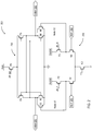
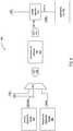
- FIG. 1 depicts a quantizer in accordance with a first implementation of the present disclosure having a STRONGARM®-type topology.
- a quantizer circuit 100 for digitizing an analog signal is presented that includes an input circuit, a regeneration circuit and a reset circuit.
- the input circuit 110 includes a plurality of input field effect transistors 112 and is coupled to a first voltage supply 120 that supplies an input signal at a first voltage, represented herein as Avccrst.
- the input circuit 110 is configured to receive a first time varying first clock signal (clk). The input circuit does not draw current when the first clock signal is below a threshold voltage and is active and consumes current when the first clock signal is above a threshold voltage.
- the regeneration circuit 130 is coupled to the input circuit 110, and includes a plurality of regeneration field effect transistors 132, 134.
- the regeneration circuit is connected to a second voltage supply 140 at a second voltage Avcc.
- the second voltage Avcc is different in magnitude from the first voltage Avccrst (higher or lower, as desired) to bring about desired performance improvements as set forth herein.
- the reset circuit 170 is coupled to the input circuit 110 and the regeneration circuit 130.
- the reset circuit 170 includes a first set of transistors 172 that couple the input circuit 110 to the first voltage supply 120, and a second set of transistors 174 that couple the regeneration circuit 130 to the second voltage supply 140, and a third transistor 178 that couples output pin 161 to output pin 162.
- the devices in input circuit 110 operate in saturation for as much of the active cycle as possible, albeit at the expense of timing performance as eventually all the devices enter the linear region (exit the saturation region) as regeneration occurs.
- the device N0 enters the linear region first once the voltage on its drain is less than Avcc -Vth0. This is followed later by devices N1 and N2 entering the linear region when nodes X1 and X2 become less than (Vcm-Vth1) and (Vcm-Vth2) respectively, wherein Vcm is the common mode voltage at the inputs 151,152 and Vth0, Vth1 and Vth2 are the respective threshold voltages of devices N0, N1 and N2.
- the input sampling phase ends approximately at the same time that N1 and N2 enter the linear region.
- the regeneration circuit 130 amplifies the differential voltage, generated by the input circuit across nodes X1 and X2 (and also by N3/N4 across output pins 161, 162) during the input sampling phase, using positive feedback to create large signal voltages close to CMOS levels at output pins 161, 162.
- Advantages in accordance with the disclosure originate from providing multiple voltage supplies to the quantizer 100, and in some embodiments, varying the relative voltage levels of the voltage supplies.
- Input referred RMS noise and input referred offset voltage can both be reduced by increasing the quantizer gain.
- the exemplary quantizers illustrated herein are illustrated without offset correction.
- quantizers of all static and dynamic topologies can usually be provided with input referred voltage offset correction based on either current/voltage or capacitive correction as are known in the art.
- the quantizer 100 operates in a sequence of phases as set forth above, the gain in earlier phases provide greater reduction of input referred RMS noise and offset voltage. Thus, by increasing the gain in the first phase of quantizer operation, input referred RMS noise and offset voltage can be reduced. Thus, Avccrst can be adjusted, or simply fixed to a value that is greater than Avcc to reduce RMS noise and voltage offset.
- Avccrst can be adjusted, or simply fixed to a value that is less than Avcc to reduce clock-to-q and improve timing.
- Avccrst can be controlled to be set at a value that tracks a combination of process, voltage and temperature (PVT) to improve timing and reduce RMS noise and voltage offset over various operating conditions of the quantizer.
- quantizers can compensate for an increase in input common mode voltage (Vcm) with minimal power increase. This is particularly advantageous where supply voltages scale down with geometry.
- Quantizers normally are placed at the boundary between the analog and digital signal processing. This usually means that its input is delivered from a higher analog supply domain than its own digital supply domain (e.g., Avcc). The average of this input is called the common mode input voltage, Vcm. High Vcm values reduce gain and thus increase RMS noise and offset voltage.
- digital supply also reduces (e.g. from 0.85v to 0.75v), for example, to mitigate reliability issues, to reduce digital power consumption for fixed processing performance, or to increase digital processing performance for constant or reduced power consumption. Accordingly, the analog supply does not reduce or its reduction is less than the digital supply reduction which means the Vcm of the quantizer has effectively been raised relative to the new lower Avcc value of the quantizer.
- the skilled artisan would only have two options with respect to the present sense amplifier (e.g., STRONGARM®-type) quantizer topologies.
- the latter option results in having to tolerate higher power consumption in quantizer, needing to add a regulator to generate an older, unscaled Avcc level, and to level shift the quantizer output down to Avcc.
- Avccrst can retain the older, unscaled Avcc supply voltage level (e.g. 0.85v). This preserves gain and thus RMS noise and offset voltage are improved.
- the remainder of quantizer is then powered by the scaled Avcc level (e.g. 0.75v).
- Avccrst can be fixed, or it can be varied in a controlled manner, depending on the desired application.
- the first voltage (Avccrst) and second voltage (Avcc) can be fixed relative to one another.
- the first voltage (Avccrst) can be proportional to or derived from the second voltage (Avcc).
- the first voltage (Avccrst) can be higher than the second voltage (Avcc) to reduce noise and voltage offset in the quantizer circuit.
- the first voltage (Avccrst) can be lower than the second voltage (Avcc) to improve timing performance of the quantizer circuit, as described above.
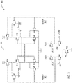
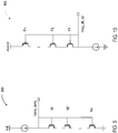
- FIGS. 2 and 3 depict further embodiments of quantizers 200, 300, respectively in accordance with the present disclosure.
- Quantizers 200, 300 are of the "double tail" type, and include input circuits 210 and 310, respectively.
- Each of the input circuits includes N0, N1, N2, N5 and N6 (wherein N5 and N6 provide additional gain) and a regeneration circuit 230, 330 including N3, N4, P4 and P5 (and N7 and N8 in the case of circuit 300).
- N7 and N8 can be considered to be a part of the reset circuit for simplicity, although they also provide additional gain as they combine with P0 and P1 ( FIG. 3 ).
- Each of circuits 210, 230 has separate currents which allow input stage gain and regeneration stage timing to be optimized separately.
- the input devices N1, N2, N5, N6 have separate currents from the regeneration devices (N3, N4, P4, P5).
- the quantizer 200 of FIG. 2 includes a dual phase clock, whereas the quantizer of FIG. 3 includes a single phase clock.
- the embodiment of FIG. 3 includes an extra gain path from Nodes X1, X2 to out, outb by way of P0, P1, N7, N8.
- the input circuit 210, 310 integrates the input in exactly the same way as the embodiment of FIG. 1 onto nodes X1 and X2.
- Input circuit 210, 310 contributes gain from the input 251, 252 (351, 352) as long as the input devices N1 and N2 are saturated.
- Avccrst pins it is possible to increase the initial voltage as with the embodiment of FIG. 1 .
- Increasing the initial starting voltage in such a manner has the same practical effect as reducing the tail current in terms of increasing the time that occurs before the input pair N1, N2 come out of saturation. This increases integration time and therefore increases gain, and thus reduces RMS noise and offset voltage.
- the second voltage can be at ground and the first voltage can be lower than the second voltage to reduce noise and voltage offset in the quantizer circuit.
- the second voltage can be at ground, and the first voltage can be higher than the second voltage to improve timing performance of the quantizer circuit.
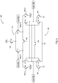
- FIG. 4 , 5 and 6 depict quantizers 400, 500, 600 in accordance with further implementations of the present disclosure.
- Vcm common mode voltage
- the quantizers 100, 200 described herein above have NMOS input pair(s) which are suited to a high input Vcm.
- Each of the aforementioned quantizers can be inverted from a high input Vcm, NMOS input pair(s) quantizer to a low input Vcm, PMOS input pair(s) quantizer.
- the low input Vcm, PMOS input pair(s) quantizers of FIGS. 4-6 all integrate the input in the input circuits (410, 510, 610) onto nodes X1 and X2 in the same way as the embodiments of FIGS. 1-3 .
- the input circuit of these embodiments contributes gain from the input as long as the input devices P1 and P2 are saturated.
- the drains are reset to Avss and are then pulled upwards towards Avcc by the common mode current.
- the initial voltage can be decreased by adding pins to apply Avssrst rather than Avss.
- Avssrst This acts to decrease the initial voltage Avssrst to a voltage less than ground (Avss), resulting in increased integration time, which in turn increases gain and decreases input referred RMS noise and input offset voltage. Conversely, increasing Avssrst to a voltage that is greater than ground decreases integration time, which increases timing performance by reducing clock-to-q.
- the level of Avssrst can be fixed, or varied over PVT in an optimized manner to improve both input referred RMS noise and input offset voltage, and/or timing performance.
- embodiments of a control circuit are provided that are configured to increase or decrease the magnitude of the first voltage with respect to Avcc or Avss for operating quantizers in accordance with the present disclosure.
- the control circuit can include an analog control circuit 700 that is configured to generate a reference signal representative of the first voltage.
- a regulator 710 can be provided that is in operable communication with the analog control circuit 700.
- the regulator 710 can be configured to output the first voltage to the quantizer circuit in response to the reference signal that is representative of the first voltage.
- the analog control circuit can generate the reference signal (Vref_reg) in response to a plurality of input signals (702, 704, Avcc, Vcm).
- the input signals can include signals indicative of at least one of the magnitude of the second voltage, a process dependent voltage, a temperature dependent voltage, or a shift voltage.
- FIG. 7B depicts a possible implementation of a summer used in the control circuit of FIG.
- process dependent voltage and temperature dependent voltage inputs can be provided to a programmable switch or summer 706 which is then processed in circuit 720 to produce the reference voltage which is outputted to the regulator.
- the control circuit 800 can include at least one analog to digital converter 808 that is configured to receive a plurality of input signals and generate digital input signal data, a programmable integrated circuit (810) operably coupled to the at least one analog-to-digital converter (“ADC") 808, the programmable integrated circuit (810) being configured to process the digital input signal data to determine circuit configuration data and generate a circuit configuration data digital output signal, and at least one digital to analog converter (812) operably coupled to the processor.
- the at least one digital to analog converter can be configured to convert the circuit configuration data digital output signal into the reference signal representative of the first voltage.
- the input signals can include signals indicative of at least one of the magnitude of the second voltage, a magnitude of the common mode voltage (Vcm), a process dependent voltage 802, a temperature dependent voltage 804, or a shift voltage.
- Vcm common mode voltage
- a single ADC and a multiplexer can sequentially poll these four analog inputs to generate a digital code from the selected analog input signal.
- the control circuit (800) can further include a regulator (814) in operable communication with the at least one digital to analog converter (812).
- the regulator can be configured to output the first voltage (Avccrst) to the quantizer circuit in response to the reference signal (Vref_reg) that is representative of the first voltage.
- the programmable integrated circuit (810) can be programmed with executable code for determining the configuration data.
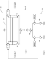
- FIG. 9 depicts a circuit 900 for analog process and temperature dependent voltage generation in accordance with the present disclosure.
- the analog Vref_reg generation circuit needs an analog process and temperature dependent voltage (Vproc_temp).
- Vproc_temp analog process and temperature dependent voltage
- FIG. 9 a current is forced into a stack of X NMOS devices. The number of devices, X, is chosen to set the required Vproc_temp. The device at the top of the stack can be selected to match N3/N4 in the circuit (e.g., 100) order to track Vt, and lower devices can be selected to match i/p beta (N1/N2) and track gm.
- FIG. 10 depicts a circuit 950 for generating a low side reference for a regulator that supplies a clock generator that generates a clock signal in accordance with the present disclosure.
- the input circuit e.g., 110
- the magnitude of the second clock signal can be generated with reference to the first clock signal.
- the second clock signal (clk_hi) can be generated by a circuit that is configured to receive a signal indicative of the first clock signal and is supplied from a regulator that is configured to receive a low side reference voltage.
- the reset devices P2, P3 in the quantizer need a clock (clk_hi) that has a logic High level of Avccrst rather than Avcc.
- the clock buffer for the quantizer 100 generates a clock named clk which has a logic High level of Avcc.
- Clk_hi can be generated from clk using a high speed, AC coupled clock generator as described in the literature.
- the low logic level of this clock, clk_hi cannot be zero volts zero volts in modern CMOS processes when Avccrst > Avcc. That would create reliability problems.
- Vneg_clk_ref a new logic low level for the clk_hi generator. This is in turn generated by a regulator which has reference Vneg_clk_ref. However, when Avccrst ⁇ Avcc and is at its minimum value the value of Vneg_clk_ref must float downwards with Avccrst towards Avss. To do this Vneg_clk_ref is generated with respect to Avccrst supply.
- the reference is implemented as a stack of PMOS devices (P1... Px) as illustrated in FIG. 10 which are matched to P2, P3 in the quantizer.
- the disclosure further contemplates the bulk or well connection of the devices (100, 200).
- PMOS devices have their bulk connection tied to the highest voltage supply which is normally Avcc as illustrated in the present Figures.
- NMOS devices have their bulk connection tied to the lowest voltage supply which is normally Avss in these diagrams.
- Avccrst and Avssrst means that Avcc and Avss are not necessarily the highest and lowest supplies, respectively. It is easiest to retain the Avcc and Avss bulk connection for all PMOS and NMOS devices disclosed herein, respectively, except for the reset devices connected to Avccrst or Avssrst.
- CMOS processes typically use a p-substrate with electrically isolated N-wells.
- PMOS devices reside in N-wells.
- the N-wells can be at different potentials and are connected to one or many positive supply voltages.
- NMOS devices reside in P-wells which are not electrically isolated from the p-substrate.
- the p-substrate is typically connected to zero volts and is usually denoted as Gnd or Avss.
- Avssrst ⁇ Avss is believed to be facilitated by either (a) a deep N-well to create electrically isolated p-substrate islands on p-substrate process, or (b) n-substrate process with electrically isolated P-wells.
- Avccrst There are two basic options to connect the bulk of PMOS reset devices powered from Avccrst. First, one can connect the bulk to Avccrst. Second, the bulk can be connected to Avcc. Similarly, the bulk of NMOS reset devices can be connected to Avssrst, or Avss. Connecting the bulk of the reset devices to Avccrst/Avssrst tends to be safer electrically, but may take up more space. This is believed to be the best connection for non-FinFET processes where non-zero values of bulk to source voltage can impair performance.
- FIG. 11 shows a programmable integrated circuit (IC) 1000 on which the disclosed circuits and processes may be implemented.
- the programmable IC may also be referred to as a System on Chip (SOC) that includes field programmable gate array logic (FPGA) along with other programmable resources.
- FPGA logic may include several different types of programmable logic blocks in the array. For example, FIG.
- FIG. 11 illustrates a programmable IC 1000 that includes a large number of different programmable tiles including multi-gigabit transceivers (MGTs) 1001, configurable logic blocks (CLBs) 1002, blocks of random access memory (BRAMs) 1003, input/output blocks (lOBs) 1004, configuration and clocking logic (CONFIG/CLOCKS) 1005, digital signal processing blocks (DSPs) 1006, specialized input/output blocks (I/O) 1007, for example, clock ports, and other programmable logic 1008 such as digital clock managers, analog-to-digital converters, system monitoring logic, and so forth.
- MTTs multi-gigabit transceivers
- CLBs configurable logic blocks
- BRAMs blocks of random access memory
- lOBs input/output blocks
- CONFIG/CLOCKS configuration and clocking logic
- DSPs digital signal processing blocks
- I/O specialized input/output blocks
- Some programmable IC having FPGA logic also include dedicated processor blocks (PRO
- each programmable tile includes a programmable interconnect element (INT) 1011 having standardized connections to and from a corresponding interconnect element in each adjacent tile. Therefore, the programmable interconnect elements taken together implement the programmable interconnect structure for the illustrated FPGA logic.
- the programmable interconnect element INT 1011 also includes the connections to and from the programmable logic element within the same tile, as shown by the examples included at the top of FIG. 11 .
- a CLB 1002 can include a configurable logic element CLE 1012 that can be programmed to implement user logic, plus a single programmable interconnect element INT 1011.
- a BRAM 1003 can include a BRAM logic element (BRL) 1013 in addition to one or more programmable interconnect elements. Often, the number of interconnect elements included in a tile depends on the height of the tile. In the pictured implementation, a BRAM tile has the same height as five CLBs, but other numbers (e.g., four) can also be used.
- a DSP tile 1006 can include a DSP logic element (DSPL) 1014 in addition to an appropriate number of programmable interconnect elements.
- DSPL DSP logic element
- An IOB 1004 can include, for example, two instances of an input/output logic element (IOL) 1015 in addition to one instance of the programmable interconnect element INT 1011.
- IOL input/output logic element
- INT programmable interconnect element
- a columnar area near the center of the die (shown shaded in FIG. 11 ) is used for configuration, clock, and other control logic.
- Horizontal areas 1009 extending from the column are used to distribute the clocks and configuration signals across the breadth of the programmable IC. Note that the references to "columnar” and “horizontal” areas are relative to viewing the drawing in a portrait orientation.
- Some programmable ICs utilizing the architecture illustrated in FIG. 11 include additional logic blocks that disrupt the regular columnar structure making up a large part of the programmable IC.
- the additional logic blocks can be programmable blocks and/or dedicated logic.
- the processor block PROC 1010 shown in FIG. 11 spans several columns of CLBs and BRAMs.
- FIG. 11 is intended to illustrate only an example of programmable IC architecture.
- the numbers of logic blocks in a column, the relative widths of the columns, the number and order of columns, the types of logic blocks included in the columns, the relative sizes of the logic blocks, and the interconnect/logic implementations included at the top of FIG. 11 are provided purely as examples.
- more than one adjacent column of CLBs is typically included wherever the CLBs appear, to facilitate the efficient implementation of user logic.
- the methods and system are thought to be applicable to a variety of systems that use RAM circuits. Other aspects and features will be apparent to those skilled in the art from consideration of the specification.
- the portions of the methods and system may be implemented as one or more processors configured to execute software, as an application specific integrated circuit (ASIC), or as a logic on a programmable logic device.
- ASIC application specific integrated circuit
- the various circuits identified herein may share hardware circuitry, such as use of a common computer processing unit or digital processing unit. It is intended that the specification and drawings be considered as examples only, with a true scope of the invention being indicated by the following claims.
Landscapes
- Physics & Mathematics (AREA)
- Nonlinear Science (AREA)
- Semiconductor Integrated Circuits (AREA)
- Analogue/Digital Conversion (AREA)
- Engineering & Computer Science (AREA)
- Theoretical Computer Science (AREA)
- Manipulation Of Pulses (AREA)
Applications Claiming Priority (2)
| Application Number | Priority Date | Filing Date | Title |
|---|---|---|---|
| US15/453,707 US9755655B1 (en) | 2017-03-08 | 2017-03-08 | Dynamic quantizers having multiple reset levels |
| PCT/US2018/018255 WO2018164818A1 (en) | 2017-03-08 | 2018-02-14 | Dynamic quantizers having multiple reset levels |
Publications (2)
| Publication Number | Publication Date |
|---|---|
| EP3593452A1 EP3593452A1 (en) | 2020-01-15 |
| EP3593452B1 true EP3593452B1 (en) | 2021-03-31 |
Family
ID=59702469
Family Applications (1)
| Application Number | Title | Priority Date | Filing Date |
|---|---|---|---|
| EP18708020.5A Active EP3593452B1 (en) | 2017-03-08 | 2018-02-14 | Dynamic quantizers having multiple reset levels |
Country Status (6)
| Country | Link |
|---|---|
| US (1) | US9755655B1 (enExample) |
| EP (1) | EP3593452B1 (enExample) |
| JP (1) | JP7274420B2 (enExample) |
| KR (1) | KR102564880B1 (enExample) |
| CN (1) | CN110521119B (enExample) |
| WO (1) | WO2018164818A1 (enExample) |
Families Citing this family (12)
| Publication number | Priority date | Publication date | Assignee | Title |
|---|---|---|---|---|
| CN107733432B (zh) * | 2017-11-10 | 2019-09-03 | 中国电子科技集团公司第五十八研究所 | 高精度电荷域流水线adc共模电荷误差校准系统 |
| CN107863962B (zh) * | 2017-11-10 | 2019-09-03 | 中国电子科技集团公司第五十八研究所 | 高精度电荷域流水线adc的电容适配误差校准系统 |
| CN107863964B (zh) * | 2017-11-10 | 2019-09-24 | 中国电子科技集团公司第五十八研究所 | 可精确控制共模电荷量的全差分电荷传输电路 |
| US10454463B1 (en) | 2018-08-21 | 2019-10-22 | Xilinx, Inc. | Adaptable quantizers having dedicated supply voltage for tail device drivers |
| WO2021200415A1 (ja) * | 2020-03-30 | 2021-10-07 | ソニーセミコンダクタソリューションズ株式会社 | コンパレータ及びアナログ-デジタル変換器 |
| WO2022018560A1 (ja) * | 2020-07-24 | 2022-01-27 | 株式会社半導体エネルギー研究所 | 半導体装置 |
| US11670345B2 (en) | 2021-02-05 | 2023-06-06 | Samsung Electronics Co., Ltd. | Sense amplifier including pre-amplifier circuit and memory device including same |
| KR20220139063A (ko) | 2021-04-07 | 2022-10-14 | 에스케이하이닉스 주식회사 | 클럭 신호 처리 회로, 반도체 장치 및 반도체 시스템 |
| US12348205B2 (en) | 2021-04-23 | 2025-07-01 | Samsung Electronics Co., Ltd. | Amplifier circuit |
| US11973621B2 (en) | 2021-12-17 | 2024-04-30 | Samsung Display Co., Ltd. | Power efficient slicer for decision feedback equalizer |
| US11664821B1 (en) * | 2022-02-08 | 2023-05-30 | SK Hynix Inc. | Error floor performance of a bit flipping decoder through identifying unreliable check nodes |
| KR102898523B1 (ko) | 2024-11-19 | 2025-12-09 | 서강대학교산학협력단 | 아날로그-디지털 변환기 |
Family Cites Families (22)
| Publication number | Priority date | Publication date | Assignee | Title |
|---|---|---|---|---|
| US4821286A (en) * | 1986-05-27 | 1989-04-11 | American Telephone And Telegraph Company | Quaternary signal regenerator |
| US6021172A (en) * | 1994-01-28 | 2000-02-01 | California Institute Of Technology | Active pixel sensor having intra-pixel charge transfer with analog-to-digital converter |
| JP2000114970A (ja) * | 1998-10-07 | 2000-04-21 | Yozan Inc | 比較回路およびアナログデジタル変換回路 |
| JP2002076901A (ja) * | 2000-08-30 | 2002-03-15 | Matsushita Electric Ind Co Ltd | Δ変調とδς変調を混合した方式の変調器,オーバーサンプリング型d/a変換器およびa/d変換器 |
| US6456215B1 (en) * | 2000-11-29 | 2002-09-24 | Raytheon Company | Method and system for quantizing an input signal |
| US6392449B1 (en) * | 2001-01-05 | 2002-05-21 | National Semiconductor Corporation | High-speed low-power low-offset hybrid comparator |
| US7288998B2 (en) * | 2003-05-02 | 2007-10-30 | Silicon Laboratories Inc. | Voltage controlled clock synthesizer |
| WO2007072588A1 (ja) * | 2005-12-20 | 2007-06-28 | Matsushita Electric Industrial Co., Ltd. | 比較器及びa/d変換器 |
| US7420497B2 (en) * | 2006-06-28 | 2008-09-02 | Broadcom Corporation | Low offset flash analog-to-digital converter |
| JP5412639B2 (ja) | 2008-10-31 | 2014-02-12 | 国立大学法人東京工業大学 | 比較器及びアナログデジタル変換器 |
| TWI382669B (zh) * | 2009-07-16 | 2013-01-11 | Ralink Technology Corp | 用於管線式類比數位轉換器之比較器及相關訊號取樣方法 |
| US8040159B1 (en) * | 2010-03-23 | 2011-10-18 | Lattice Semiconductor Corporation | Comparator with jitter mitigation |
| JP2011211371A (ja) * | 2010-03-29 | 2011-10-20 | Panasonic Corp | 逐次比較型ad変換器用クロック生成回路 |
| TWI443969B (zh) | 2010-11-17 | 2014-07-01 | Ind Tech Res Inst | 以動態比較器為基礎的比較系統 |
| JP2012227588A (ja) | 2011-04-15 | 2012-11-15 | Fujitsu Semiconductor Ltd | 比較回路及びアナログデジタル変換回路 |
| US8692582B1 (en) * | 2012-01-06 | 2014-04-08 | Altera Corporation | Latched comparator circuitry |
| JP5417470B2 (ja) | 2012-03-05 | 2014-02-12 | 株式会社半導体理工学研究センター | ダイナミックコンパレータのためのオフセット電圧補正回路とそれを用いたダイナミックコンパレータ回路 |
| JP2013187695A (ja) * | 2012-03-07 | 2013-09-19 | Sony Corp | コンパレータおよびad変換器 |
| CN102638268B (zh) * | 2012-04-19 | 2015-02-18 | 北京工业大学 | 基于逐次比较量化器的三阶前馈Sigma-Delta调制器 |
| US8730404B2 (en) * | 2012-05-31 | 2014-05-20 | Silicon Laboratories Inc. | Providing a reset mechanism for a latch circuit |
| US9287862B2 (en) * | 2013-12-26 | 2016-03-15 | Texas Instruments Incorporated | Bootstrapped sampling switch circuits and systems |
| CN104158545B (zh) * | 2014-08-14 | 2017-04-05 | 电子科技大学 | 一种基于压控振荡器量化的逐次逼近寄存器型模数转换器 |
-
2017
- 2017-03-08 US US15/453,707 patent/US9755655B1/en not_active Expired - Fee Related
-
2018
- 2018-02-14 EP EP18708020.5A patent/EP3593452B1/en active Active
- 2018-02-14 WO PCT/US2018/018255 patent/WO2018164818A1/en not_active Ceased
- 2018-02-14 CN CN201880025256.4A patent/CN110521119B/zh active Active
- 2018-02-14 JP JP2019548740A patent/JP7274420B2/ja active Active
- 2018-02-14 KR KR1020197029140A patent/KR102564880B1/ko active Active
Non-Patent Citations (1)
| Title |
|---|
| None * |
Also Published As
| Publication number | Publication date |
|---|---|
| US9755655B1 (en) | 2017-09-05 |
| EP3593452A1 (en) | 2020-01-15 |
| JP7274420B2 (ja) | 2023-05-16 |
| CN110521119A (zh) | 2019-11-29 |
| KR102564880B1 (ko) | 2023-08-07 |
| WO2018164818A1 (en) | 2018-09-13 |
| KR20190123315A (ko) | 2019-10-31 |
| CN110521119B (zh) | 2024-01-23 |
| JP2020510340A (ja) | 2020-04-02 |
Similar Documents
| Publication | Publication Date | Title |
|---|---|---|
| EP3593452B1 (en) | Dynamic quantizers having multiple reset levels | |
| US6455901B2 (en) | Semiconductor integrated circuit | |
| US9197199B2 (en) | Level shifter for high density integrated circuits | |
| US8536922B2 (en) | Clock distribution network | |
| US20150008894A1 (en) | Dynamic start-up circuit for hysteretic loop switched-capacitor voltage regulator | |
| US6525587B2 (en) | Semiconductor integrated circuit device including a clock synchronous type logical processing circuit | |
| US9548086B2 (en) | Integrated circuit device body bias circuits and methods | |
| US9870014B1 (en) | Digital low drop-out regulator | |
| GB2530238A (en) | Power gating in an electronic device | |
| US10763879B1 (en) | Low power and high-speed circuit for generating asynchronous clock signals | |
| JP2011502397A (ja) | デジタル回路内の電力消費量を低減させる補償技法 | |
| EP2775481B1 (en) | Apparatus and method for reducing sampling circuit timing mismatch | |
| CN110874111B (zh) | 具有增强的线性度的电流模式反馈源极跟随器 | |
| US8816720B2 (en) | Single power supply logic level shifter circuit | |
| US20190064866A1 (en) | Switchable power supply | |
| US20240213961A1 (en) | Clock adjustment circuit with bias scheme | |
| US10826467B1 (en) | High-accuracy dual-mode free running oscillator | |
| US9362819B1 (en) | Single capacitor, controlled output, inverter based positive/negative charge pump | |
| US20120112820A1 (en) | Circuit and method for generating body bias voltage for an integrated circuit | |
| JP7528118B2 (ja) | スイッチ漏れ補償回路 | |
| Kim et al. | PVT variation tolerant current source with on-chip digital self-calibration | |
| Kamae et al. | A forward/reverse body bias generator with wide supply-range down to threshold voltage | |
| JP2013172155A (ja) | 半導体装置 | |
| CN101622704A (zh) | 半导体器件及其复位方法 | |
| Gururani et al. | Design of 4-bit Flash ADC using double tail comparator in 130nm technology |
Legal Events
| Date | Code | Title | Description |
|---|---|---|---|
| STAA | Information on the status of an ep patent application or granted ep patent |
Free format text: STATUS: UNKNOWN |
|
| STAA | Information on the status of an ep patent application or granted ep patent |
Free format text: STATUS: THE INTERNATIONAL PUBLICATION HAS BEEN MADE |
|
| PUAI | Public reference made under article 153(3) epc to a published international application that has entered the european phase |
Free format text: ORIGINAL CODE: 0009012 |
|
| STAA | Information on the status of an ep patent application or granted ep patent |
Free format text: STATUS: REQUEST FOR EXAMINATION WAS MADE |
|
| 17P | Request for examination filed |
Effective date: 20191008 |
|
| AK | Designated contracting states |
Kind code of ref document: A1 Designated state(s): AL AT BE BG CH CY CZ DE DK EE ES FI FR GB GR HR HU IE IS IT LI LT LU LV MC MK MT NL NO PL PT RO RS SE SI SK SM TR |
|
| AX | Request for extension of the european patent |
Extension state: BA ME |
|
| DAV | Request for validation of the european patent (deleted) | ||
| DAX | Request for extension of the european patent (deleted) | ||
| GRAP | Despatch of communication of intention to grant a patent |
Free format text: ORIGINAL CODE: EPIDOSNIGR1 |
|
| STAA | Information on the status of an ep patent application or granted ep patent |
Free format text: STATUS: GRANT OF PATENT IS INTENDED |
|
| INTG | Intention to grant announced |
Effective date: 20201014 |
|
| RIN1 | Information on inventor provided before grant (corrected) |
Inventor name: HUDNER, JAMES |
|
| GRAS | Grant fee paid |
Free format text: ORIGINAL CODE: EPIDOSNIGR3 |
|
| GRAA | (expected) grant |
Free format text: ORIGINAL CODE: 0009210 |
|
| STAA | Information on the status of an ep patent application or granted ep patent |
Free format text: STATUS: THE PATENT HAS BEEN GRANTED |
|
| AK | Designated contracting states |
Kind code of ref document: B1 Designated state(s): AL AT BE BG CH CY CZ DE DK EE ES FI FR GB GR HR HU IE IS IT LI LT LU LV MC MK MT NL NO PL PT RO RS SE SI SK SM TR |
|
| REG | Reference to a national code |
Ref country code: GB Ref legal event code: FG4D Ref country code: CH Ref legal event code: EP |
|
| REG | Reference to a national code |
Ref country code: DE Ref legal event code: R096 Ref document number: 602018014750 Country of ref document: DE Ref country code: AT Ref legal event code: REF Ref document number: 1378099 Country of ref document: AT Kind code of ref document: T Effective date: 20210415 |
|
| REG | Reference to a national code |
Ref country code: IE Ref legal event code: FG4D |
|
| REG | Reference to a national code |
Ref country code: LT Ref legal event code: MG9D |
|
| PG25 | Lapsed in a contracting state [announced via postgrant information from national office to epo] |
Ref country code: NO Free format text: LAPSE BECAUSE OF FAILURE TO SUBMIT A TRANSLATION OF THE DESCRIPTION OR TO PAY THE FEE WITHIN THE PRESCRIBED TIME-LIMIT Effective date: 20210630 Ref country code: FI Free format text: LAPSE BECAUSE OF FAILURE TO SUBMIT A TRANSLATION OF THE DESCRIPTION OR TO PAY THE FEE WITHIN THE PRESCRIBED TIME-LIMIT Effective date: 20210331 Ref country code: HR Free format text: LAPSE BECAUSE OF FAILURE TO SUBMIT A TRANSLATION OF THE DESCRIPTION OR TO PAY THE FEE WITHIN THE PRESCRIBED TIME-LIMIT Effective date: 20210331 Ref country code: BG Free format text: LAPSE BECAUSE OF FAILURE TO SUBMIT A TRANSLATION OF THE DESCRIPTION OR TO PAY THE FEE WITHIN THE PRESCRIBED TIME-LIMIT Effective date: 20210630 |
|
| PG25 | Lapsed in a contracting state [announced via postgrant information from national office to epo] |
Ref country code: SE Free format text: LAPSE BECAUSE OF FAILURE TO SUBMIT A TRANSLATION OF THE DESCRIPTION OR TO PAY THE FEE WITHIN THE PRESCRIBED TIME-LIMIT Effective date: 20210331 Ref country code: RS Free format text: LAPSE BECAUSE OF FAILURE TO SUBMIT A TRANSLATION OF THE DESCRIPTION OR TO PAY THE FEE WITHIN THE PRESCRIBED TIME-LIMIT Effective date: 20210331 Ref country code: LV Free format text: LAPSE BECAUSE OF FAILURE TO SUBMIT A TRANSLATION OF THE DESCRIPTION OR TO PAY THE FEE WITHIN THE PRESCRIBED TIME-LIMIT Effective date: 20210331 |
|
| REG | Reference to a national code |
Ref country code: NL Ref legal event code: MP Effective date: 20210331 |
|
| REG | Reference to a national code |
Ref country code: AT Ref legal event code: MK05 Ref document number: 1378099 Country of ref document: AT Kind code of ref document: T Effective date: 20210331 |
|
| PG25 | Lapsed in a contracting state [announced via postgrant information from national office to epo] |
Ref country code: NL Free format text: LAPSE BECAUSE OF FAILURE TO SUBMIT A TRANSLATION OF THE DESCRIPTION OR TO PAY THE FEE WITHIN THE PRESCRIBED TIME-LIMIT Effective date: 20210331 Ref country code: SM Free format text: LAPSE BECAUSE OF FAILURE TO SUBMIT A TRANSLATION OF THE DESCRIPTION OR TO PAY THE FEE WITHIN THE PRESCRIBED TIME-LIMIT Effective date: 20210331 Ref country code: AT Free format text: LAPSE BECAUSE OF FAILURE TO SUBMIT A TRANSLATION OF THE DESCRIPTION OR TO PAY THE FEE WITHIN THE PRESCRIBED TIME-LIMIT Effective date: 20210331 Ref country code: LT Free format text: LAPSE BECAUSE OF FAILURE TO SUBMIT A TRANSLATION OF THE DESCRIPTION OR TO PAY THE FEE WITHIN THE PRESCRIBED TIME-LIMIT Effective date: 20210331 Ref country code: EE Free format text: LAPSE BECAUSE OF FAILURE TO SUBMIT A TRANSLATION OF THE DESCRIPTION OR TO PAY THE FEE WITHIN THE PRESCRIBED TIME-LIMIT Effective date: 20210331 Ref country code: CZ Free format text: LAPSE BECAUSE OF FAILURE TO SUBMIT A TRANSLATION OF THE DESCRIPTION OR TO PAY THE FEE WITHIN THE PRESCRIBED TIME-LIMIT Effective date: 20210331 |
|
| PG25 | Lapsed in a contracting state [announced via postgrant information from national office to epo] |
Ref country code: SK Free format text: LAPSE BECAUSE OF FAILURE TO SUBMIT A TRANSLATION OF THE DESCRIPTION OR TO PAY THE FEE WITHIN THE PRESCRIBED TIME-LIMIT Effective date: 20210331 Ref country code: RO Free format text: LAPSE BECAUSE OF FAILURE TO SUBMIT A TRANSLATION OF THE DESCRIPTION OR TO PAY THE FEE WITHIN THE PRESCRIBED TIME-LIMIT Effective date: 20210331 Ref country code: PT Free format text: LAPSE BECAUSE OF FAILURE TO SUBMIT A TRANSLATION OF THE DESCRIPTION OR TO PAY THE FEE WITHIN THE PRESCRIBED TIME-LIMIT Effective date: 20210802 Ref country code: PL Free format text: LAPSE BECAUSE OF FAILURE TO SUBMIT A TRANSLATION OF THE DESCRIPTION OR TO PAY THE FEE WITHIN THE PRESCRIBED TIME-LIMIT Effective date: 20210331 Ref country code: IS Free format text: LAPSE BECAUSE OF FAILURE TO SUBMIT A TRANSLATION OF THE DESCRIPTION OR TO PAY THE FEE WITHIN THE PRESCRIBED TIME-LIMIT Effective date: 20210731 |
|
| REG | Reference to a national code |
Ref country code: DE Ref legal event code: R097 Ref document number: 602018014750 Country of ref document: DE |
|
| PG25 | Lapsed in a contracting state [announced via postgrant information from national office to epo] |
Ref country code: AL Free format text: LAPSE BECAUSE OF FAILURE TO SUBMIT A TRANSLATION OF THE DESCRIPTION OR TO PAY THE FEE WITHIN THE PRESCRIBED TIME-LIMIT Effective date: 20210331 Ref country code: DK Free format text: LAPSE BECAUSE OF FAILURE TO SUBMIT A TRANSLATION OF THE DESCRIPTION OR TO PAY THE FEE WITHIN THE PRESCRIBED TIME-LIMIT Effective date: 20210331 Ref country code: ES Free format text: LAPSE BECAUSE OF FAILURE TO SUBMIT A TRANSLATION OF THE DESCRIPTION OR TO PAY THE FEE WITHIN THE PRESCRIBED TIME-LIMIT Effective date: 20210331 |
|
| PLBE | No opposition filed within time limit |
Free format text: ORIGINAL CODE: 0009261 |
|
| STAA | Information on the status of an ep patent application or granted ep patent |
Free format text: STATUS: NO OPPOSITION FILED WITHIN TIME LIMIT |
|
| 26N | No opposition filed |
Effective date: 20220104 |
|
| PG25 | Lapsed in a contracting state [announced via postgrant information from national office to epo] |
Ref country code: IS Free format text: LAPSE BECAUSE OF FAILURE TO SUBMIT A TRANSLATION OF THE DESCRIPTION OR TO PAY THE FEE WITHIN THE PRESCRIBED TIME-LIMIT Effective date: 20210731 |
|
| PG25 | Lapsed in a contracting state [announced via postgrant information from national office to epo] |
Ref country code: IT Free format text: LAPSE BECAUSE OF FAILURE TO SUBMIT A TRANSLATION OF THE DESCRIPTION OR TO PAY THE FEE WITHIN THE PRESCRIBED TIME-LIMIT Effective date: 20210331 |
|
| PG25 | Lapsed in a contracting state [announced via postgrant information from national office to epo] |
Ref country code: MC Free format text: LAPSE BECAUSE OF FAILURE TO SUBMIT A TRANSLATION OF THE DESCRIPTION OR TO PAY THE FEE WITHIN THE PRESCRIBED TIME-LIMIT Effective date: 20210331 |
|
| REG | Reference to a national code |
Ref country code: CH Ref legal event code: PL |
|
| REG | Reference to a national code |
Ref country code: BE Ref legal event code: MM Effective date: 20220228 |
|
| PG25 | Lapsed in a contracting state [announced via postgrant information from national office to epo] |
Ref country code: LU Free format text: LAPSE BECAUSE OF NON-PAYMENT OF DUE FEES Effective date: 20220214 |
|
| PG25 | Lapsed in a contracting state [announced via postgrant information from national office to epo] |
Ref country code: LI Free format text: LAPSE BECAUSE OF NON-PAYMENT OF DUE FEES Effective date: 20220228 Ref country code: CH Free format text: LAPSE BECAUSE OF NON-PAYMENT OF DUE FEES Effective date: 20220228 |
|
| PG25 | Lapsed in a contracting state [announced via postgrant information from national office to epo] |
Ref country code: BE Free format text: LAPSE BECAUSE OF NON-PAYMENT OF DUE FEES Effective date: 20220228 |
|
| P01 | Opt-out of the competence of the unified patent court (upc) registered |
Effective date: 20230530 |
|
| PG25 | Lapsed in a contracting state [announced via postgrant information from national office to epo] |
Ref country code: MK Free format text: LAPSE BECAUSE OF FAILURE TO SUBMIT A TRANSLATION OF THE DESCRIPTION OR TO PAY THE FEE WITHIN THE PRESCRIBED TIME-LIMIT Effective date: 20210331 Ref country code: CY Free format text: LAPSE BECAUSE OF FAILURE TO SUBMIT A TRANSLATION OF THE DESCRIPTION OR TO PAY THE FEE WITHIN THE PRESCRIBED TIME-LIMIT Effective date: 20210331 |
|
| PG25 | Lapsed in a contracting state [announced via postgrant information from national office to epo] |
Ref country code: HU Free format text: LAPSE BECAUSE OF FAILURE TO SUBMIT A TRANSLATION OF THE DESCRIPTION OR TO PAY THE FEE WITHIN THE PRESCRIBED TIME-LIMIT; INVALID AB INITIO Effective date: 20180214 |
|
| PG25 | Lapsed in a contracting state [announced via postgrant information from national office to epo] |
Ref country code: MT Free format text: LAPSE BECAUSE OF FAILURE TO SUBMIT A TRANSLATION OF THE DESCRIPTION OR TO PAY THE FEE WITHIN THE PRESCRIBED TIME-LIMIT Effective date: 20210331 |
|
| PG25 | Lapsed in a contracting state [announced via postgrant information from national office to epo] |
Ref country code: GR Free format text: LAPSE BECAUSE OF NON-PAYMENT OF DUE FEES Effective date: 20210331 |
|
| PG25 | Lapsed in a contracting state [announced via postgrant information from national office to epo] |
Ref country code: GR Free format text: LAPSE BECAUSE OF NON-PAYMENT OF DUE FEES Effective date: 20210331 |
|
| PGFP | Annual fee paid to national office [announced via postgrant information from national office to epo] |
Ref country code: DE Payment date: 20250128 Year of fee payment: 8 |
|
| PGFP | Annual fee paid to national office [announced via postgrant information from national office to epo] |
Ref country code: IE Payment date: 20250204 Year of fee payment: 8 |
|
| PGFP | Annual fee paid to national office [announced via postgrant information from national office to epo] |
Ref country code: FR Payment date: 20250219 Year of fee payment: 8 |
|
| PGFP | Annual fee paid to national office [announced via postgrant information from national office to epo] |
Ref country code: GB Payment date: 20250210 Year of fee payment: 8 |
|
| PG25 | Lapsed in a contracting state [announced via postgrant information from national office to epo] |
Ref country code: TR Free format text: LAPSE BECAUSE OF FAILURE TO SUBMIT A TRANSLATION OF THE DESCRIPTION OR TO PAY THE FEE WITHIN THE PRESCRIBED TIME-LIMIT Effective date: 20210331 |