EP3550371A1 - Entwicklungsvorrichtung - Google Patents
Entwicklungsvorrichtung Download PDFInfo
- Publication number
- EP3550371A1 EP3550371A1 EP19165860.8A EP19165860A EP3550371A1 EP 3550371 A1 EP3550371 A1 EP 3550371A1 EP 19165860 A EP19165860 A EP 19165860A EP 3550371 A1 EP3550371 A1 EP 3550371A1
- Authority
- EP
- European Patent Office
- Prior art keywords
- developer
- gap
- axis
- section
- developing roller
- Prior art date
- Legal status (The legal status is an assumption and is not a legal conclusion. Google has not performed a legal analysis and makes no representation as to the accuracy of the status listed.)
- Withdrawn
Links
Images


Classifications
-
- G—PHYSICS
- G03—PHOTOGRAPHY; CINEMATOGRAPHY; ANALOGOUS TECHNIQUES USING WAVES OTHER THAN OPTICAL WAVES; ELECTROGRAPHY; HOLOGRAPHY
- G03G—ELECTROGRAPHY; ELECTROPHOTOGRAPHY; MAGNETOGRAPHY
- G03G15/00—Apparatus for electrographic processes using a charge pattern
- G03G15/06—Apparatus for electrographic processes using a charge pattern for developing
- G03G15/08—Apparatus for electrographic processes using a charge pattern for developing using a solid developer, e.g. powder developer
- G03G15/0822—Arrangements for preparing, mixing, supplying or dispensing developer
- G03G15/0865—Arrangements for supplying new developer
-
- G—PHYSICS
- G03—PHOTOGRAPHY; CINEMATOGRAPHY; ANALOGOUS TECHNIQUES USING WAVES OTHER THAN OPTICAL WAVES; ELECTROGRAPHY; HOLOGRAPHY
- G03G—ELECTROGRAPHY; ELECTROPHOTOGRAPHY; MAGNETOGRAPHY
- G03G15/00—Apparatus for electrographic processes using a charge pattern
- G03G15/06—Apparatus for electrographic processes using a charge pattern for developing
- G03G15/08—Apparatus for electrographic processes using a charge pattern for developing using a solid developer, e.g. powder developer
- G03G15/0806—Apparatus for electrographic processes using a charge pattern for developing using a solid developer, e.g. powder developer on a donor element, e.g. belt, roller
- G03G15/0812—Apparatus for electrographic processes using a charge pattern for developing using a solid developer, e.g. powder developer on a donor element, e.g. belt, roller characterised by the developer regulating means, e.g. structure of doctor blade
-
- G—PHYSICS
- G03—PHOTOGRAPHY; CINEMATOGRAPHY; ANALOGOUS TECHNIQUES USING WAVES OTHER THAN OPTICAL WAVES; ELECTROGRAPHY; HOLOGRAPHY
- G03G—ELECTROGRAPHY; ELECTROPHOTOGRAPHY; MAGNETOGRAPHY
- G03G15/00—Apparatus for electrographic processes using a charge pattern
- G03G15/06—Apparatus for electrographic processes using a charge pattern for developing
- G03G15/08—Apparatus for electrographic processes using a charge pattern for developing using a solid developer, e.g. powder developer
- G03G15/0806—Apparatus for electrographic processes using a charge pattern for developing using a solid developer, e.g. powder developer on a donor element, e.g. belt, roller
- G03G15/081—Apparatus for electrographic processes using a charge pattern for developing using a solid developer, e.g. powder developer on a donor element, e.g. belt, roller characterised by the developer handling means after the supply and before the regulating, e.g. means for preventing developer blocking
-
- G—PHYSICS
- G03—PHOTOGRAPHY; CINEMATOGRAPHY; ANALOGOUS TECHNIQUES USING WAVES OTHER THAN OPTICAL WAVES; ELECTROGRAPHY; HOLOGRAPHY
- G03G—ELECTROGRAPHY; ELECTROPHOTOGRAPHY; MAGNETOGRAPHY
- G03G9/00—Developers
Definitions
- the present invention relates to a developing device for forming a visible image by developing an electrostatic latent image formed on an image bearing member by an electrophotographic type, an electrostatic recording type or the like, and particularly relates to a structure including a coating amounting portion for regulating a coating amount of a developer carried on a developer carrying member.
- An image forming apparatus such as a copying machine, a printer, a facsimile machine or a multi-function machine of these machines conventionally includes the developing device for forming the visible image by developing the electrostatic latent image formed on a photosensitive drum as the image bearing member by the electrophotographic type, the electrostatic recording type or the like.
- a developing device carries and feeds the developer by a magnetic force at a surface of a developing sleeve as the developer carrying member. Then, a coating amount (layer thickness) of the developer on the developing sleeve surface is uniformized by a doctor blade as a coating amount regulating portion for regulating the coating amount of the carried developer, so that stable supply of the developer to the photosensitive drum (photosensitive member) is realized.
- the developer scraped off by the doctor blade is liable to stagnate in an upstream side of a gap between the doctor blade and the developing sleeve (hereinafter referred to as an "SB gap").
- SB gap a gap between the doctor blade and the developing sleeve
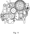
- the SB gap is subjected to the following adjustment for ensuring the SB gap with accuracy of, e.g., about ⁇ 30 - 50 ⁇ m in order to obtain an optimum development density. That is, as shown in Figure 11 , a constitution such that a projection amount of a doctor blade 73 to the developing sleeve 70 is adjusted and is fixed with an adjusting screw 75 to a developer station limiting member 76 as a base is employed.
- the SB gap is measured at a plurality of positions with respect to the longitudinal direction, and also the adjusting screw 75 is provided similarly at a plurality of positions with respect to the longitudinal direction.
- a principal flow of the developer can be regarded as a flow of the developer carried and fed by the magnetic force of the developing sleeve 70 (i.e., a developer flow in a region toward the developing sleeve with a boundary indicated by an arrow Fm in (a) of Figure 12 , hereinafter simply referred to as a mainstream (main flow) Fm).
- a mainstream Fm a part of the mainstream Fm is cut at a stepped portion 77 between the developer station limiting member 76 and the doctor blade 73, and therefore another flow Fs obstructing the mainstream Fm (hereinafter simply referred to as a sidestream (side flow) Fs) is caused to be generated.
- This sidestream Fs generates, as shown in (a) of Figure 12 , a circulating flow which forms a station layer in the upstream side of the doctor blade 73 and constitutes a shearing flow at a boundary between the mainstream Fm and the sidestream Fs.
- the mainstream Fm is influenced by the sidestream Fs in the upstream side of the SB gap, so that the coating amount of the developer carried on the developing sleeve 70 is liable to be unstable and therefore a stable development density cannot be obtained in some cases.
- a principal object of the present invention is to provide a developing device and a regulating member which are capable of realizing a structure by which a stable development density can be obtained without requiring high part accuracy and high adjustment accuracy.
- a developing device comprising: a developer carrying member for carrying and feeding a developer; a regulating portion for regulating a coating amount of the developer carried on the developer carrying member, wherein the regulating portion includes an edge portion at a closest position to a surface of the developer carrying member or includes a flat portion tilted, at the closest position, by an angle of 2 degrees or less relative to a contact flat plane contacting the surface of the developer carrying member; and a rectifying portion for rectifying a flow of the developer, wherein the rectifying portion is connected with the edge portion or an upstream end of the flat portion in an upstream side of the regulating portion, with respect to a developer feeding direction, wherein in a cross section perpendicular to an axial direction of the developer carrying member, when coordinates are set such that the upper end of the flat portion or the edge portion is an origin E, a direction which is parallel to the contact flat plane and which is opposite to the developer feeding direction is a positive side of X-axis, a direction
- a regulating member provided opposed to a developer carrying member for carrying a developer, for regulating the developer to be coated on the developer carrying member, the regulating member comprising: a regulating portion for regulating a coating amount of the developer carried on the developer carrying member, wherein the regulating portion includes an edge portion at a closest position to a surface of the developer carrying member or includes a flat portion tilted, at the closest position, by an angle of 2 degrees or less relative to a contact flat plane contacting the surface of the developer carrying member; and a rectifying portion for rectifying a flow of the developer, wherein the rectifying portion is connected with the edge portion or an upstream end of the flat portion in an upstream side of the regulating portion, with respect to a developer feeding direction, wherein in a cross section perpendicular to an axial direction of the developer carrying member, when coordinates are set such that the upper end of the flat portion or the edge portion is an origin E, a direction which is parallel to the contact flat plane and which is
- Figure 1 is a sectional view of a color image forming apparatus of an electrophotographic type
- an image forming apparatus 60 is an example of the image forming apparatus of a so-called intermediary transfer tandem type in which image forming portions (process cartridges) 600 for four colors are provided opposed to an intermediary transfer belt 61.
- the intermediary transfer tandem type is a mainstream constitution in recent years from a viewpoint of high productivity and a viewpoint that it can meet feeding of various media.
- a feeding process of a recording material S in such an image forming apparatus 60 will be described.
- the recording material S is accommodated in a recording material storage (cassette) 62 in a stacked manner, and is fed by a sheet feeding roller 63 at image forming timing.
- the recording material S fed by a sheet feeding roller 63 is fed to a registration roller 65 provided in a halfway position of a feeding path 64. Then, oblique movement correction and timing correction of the recording material S are made by the registration roller65, and thereafter the recording material S is fed to a secondary transfer portion T2.
- the secondary transfer portion T2 is a transfer nip formed by opposing rollers consisting of a secondary transfer inner roller 66 and a secondary transfer outer roller 67, and a toner image is attracted to the recording material S by applying a predetermined pressure and a predetermined electrostatic load bias.
- the feeding process of the recording material S to the secondary transfer portion T2 is described above.
- a formation method of an image sent to the secondary transfer portion T2 at the same timing will be described.
- the image forming portions 600 will be described, but the image forming portions 600 for respective colors basically have the same constitution except for the colors of toners, and therefore the image forming portion 600 for black (Bk) will be described as a representative.
- the image forming portion 600 is constituted principally by a photosensitive drum (photosensitive member, image bearing member) 1, a charging device 2, a developing device 3, a photosensitive drum cleaner 5 and the like.
- a surface of the photosensitive drum 1 to be rotationally driven is electrically charged uniformly in advance by the charging device 2, and then an electrostatic latent image is formed by an exposure device 68 driven on the basis of an image information signal.
- the electrostatic latent image formed on the photosensitive drum 1 is subjected to development with a toner by the developing device to be visualized.
- the toner image formed on the photosensitive drum 1 is primary-transferred onto the intermediary transfer belt 61 by providing a predetermined pressure and a predetermined electrostatic load bias by a primary transfer device 5 provided opposed to the image forming portion 600 via the intermediary transfer belt 61.
- a transfer residual toner remaining on the photosensitive drum 1 in a slight amount is collected by the photosensitive drum cleaner 5, and then is subjected to a subsequent image forming process.
- the number of the colors is not limited to 4, and also the order of arrangement of these image forming portions of the respective colors is not limited to the above order.
- the intermediary transfer belt 61 is stretched by a tension roller 6, the secondary transfer inner roller 66 and follower rollers 7a and 7b, and is an endless belt to be fed and driven in an arrow C direction in Figure 1 .
- the secondary transfer inner roller 66 also functions as a driving roller for driving the intermediary transfer belt 61.
- the image forming processes, for the respective colors, provided in parallel by the above-described respective image forming portions 600 for Y, M, C and Bk are performed at timing when the toner images are successively superposed on the upstream color toner images primary-transferred onto the intermediary transfer belt 61.
- a fall-color toner image is finally formed on the intermediary transfer belt 61 and then is fed to the secondary transfer portion T2.
- a transfer residual toner passing through the secondary transfer portion T2 is collected by a transfer cleaner device 8.
- timing of the recording material S and timing of the full-color toner image are coincide with each other at the secondary transfer portion T2, where secondary transfer is effected.
- the recording material S is fed to a fixing device 9, where the toner image is melted and fixed on the recording material S by predetermined pressure and heat quantity.
- the thus image-fixed recording material S is subjected to selection such that the recording material S is discharged onto a discharge tray 601 as it is by normal rotation of a sheet discharging roller 69 or is subjected to double-side image formation.
- the developing device 3 in this embodiment will be described with reference to Figures 2 and 3 .
- a developer a two-change developer obtained by mixing the toner and a magnetic carrier is used.
- the toner is supplied from a toner cartridge 605 ( Figure 1 ) set in the image forming apparatus 60 into a developing container 30 via an unshown toner feeding path.
- a first feeding chamber 31 and a second feeding chamber 32 which are partitioned by a partition wall are provided and are connected with each other at their end portions with respect to a longitudinal direction.
- a first feeding screw 33 and a second feeding screw 34 are rotatably supported in the first feeding chamber 31 and the second feeding chamber 32, respectively, and are driven to circulate the fed toner through the two feeding chambers.
- the magnetic carrier is contained in advance in the developing container in the developing container 30, and the toner is sufficiently stirred with the magnetic carrier during the circulation in the first feeding chamber 31 to be triboelectrically charged, so that the toner and the magnetic carrier are fed to the second feeding chamber 32.
- the second feeding screw 34 in the second feeding chamber 32 is disposed opposed to a developing sleeve 70 as a developer carrying member and performs the function of feeding and supplying the toner, deposited on the magnetic carrier by the triboelectric charge with the magnetic carrier.
- the developing sleeve 70 carries and feeds the developer by a magnetic force and has a constitution in which a magnet portion 71 where a pattern of magnetic poles for generating a desired magnetic field is provided therein and a sleeve pipe 72 is covered over an outside of the magnet portion 71.
- the magnet portion 71 is supported in a non-rotational manner so that the magnetic pole pattern is fixed at a predetermined phase with respect to a circumferential direction, and only the sleeve pipe 72 is rotatably supported.
- the magnetic carrier supplied from the second feeding screw 34 is carried in an erected state on the surface of the developing sleeve 70 together with the toner deposited thereon by the triboelectric charge, and then is fed in an arrow E direction in Figure 2 .
- the rotational direction E of the developing sleeve 70 is set so as to be counterdirectional to the rotational direction D of the photosensitive drum 1, but may also be set so as to be the same direction as the rotational direction D of the photosensitive drum 1.
- a developer rectifying portion 35 and a coating amount regulating portion 36 and the photosensitive drum 1 are provided as members opposing the surface of the developing sleeve 70.
- the developer rectifying portion 35 and the coating amount regulating portion 36 are integrally formed of a resin material as a non-magnetic material, and constitute a sleeve holder frame 37.
- the sleeve holder frame 37 is, e.g., formed by molding the resin material.
- the resin material for the sleeve holder frame 37 it is possible to use PC (polycarbonate) + AS (acrylonitrile-styrene copolymer), PC + ABS (acrylonitrile-butadiene-styrene copolymer), and the like. Further, a fiber material such as glass or carbon may preferably be incorporated into such a resin material.
- the material for the sleeve holder frame 37 is not limited to the resin material but may also be a non-magnetic metal material such as an aluminum alloy.
- the sleeve holder frame 37 may also be formed by aluminum die-cast.
- the developer rectifying portion 35 and the coating amount regulating portion 36 may be constituted as separate members and may be connected with each other.
- Figure 3 shows a supporting structure of the developing sleeve 70 by the sleeve holder frame 37.
- the sleeve holder frame 37 constitutes a sleeve holder unit 10 together with sleeve bearing members 11a and 11b provided at end portions thereof.
- An attitude of the sleeve holder unit 10 is fixed to the developing container 30 by a positioning shaft 13.
- Figure 4 shows a relationship between the developer rectifying portion 35, the coating amount regulating portion 36 and the developing sleeve 70 in the case where the sleeve holder unit is seen along a cross-section H shown in Figure 3 .
- the coating amount regulating portion 36 includes a coating amount regulating surface 36a opposing the surface of the developing sleeve 70, and regulates a coating amount of the developer carried on the developing sleeve 70.
- the developer rectifying portion 35 is disposed upstream of the coating amount regulating portion 36 with respect to a developer feeding direction (arrow E direction) of the developing sleeve 70, and has a developer rectifying surface 35a continuous to the coating amount regulating surface 36a in the developing sleeve 70 side (developer carrying member) side.
- a closest portion between the coating amount regulating portion 36 and the developing sleeve 70 (i.e., a closest position between the surface of the developing sleeve 70 and the coating amount regulating surface 36a) is defined at an entrance portion of the coating amount regulating portion 36. That is, at an upstreammost end of the coating amount regulating portion 36 with respect to the developer feeding direction, a gap (spacing) between the coating amount regulating surface 36a and the surface of the developing sleeve 70 is smallest. Accordingly, the gap (smallest gap or interval) at this position is referred to as an SB gap G.
- Adjustment of the SB gap G in this embodiment is performed by moving a position of the sleeve holder frame 37 relative to the sleeve bearing members 11a and 11b, and after falling of a value of the SB gap G within a desired range is checked by, e.g., a camera, the sleeve holder frame 37 is fixed (secured) with a screw 14 ( Figure 3 ).
- a surface thereof in the developing sleeve 70 side is a flow path wall surface for forming a developer flow path. Accordingly, the developer rectifying surface 35a and the coating amount regulating surface 36a of the developer rectifying portion 35 and the coating amount regulating portion 36, respectively, constitute a part of the flow path wall surface.
- a contact flat plane A contacting the developing sleeve 70 at the closest position between the surface of the developing sleeve 70 and the coating amount regulating surface 36a is defined.
- the developer rectifying surface 35a is formed so that a gap thereof with the contact flat plane A decreases toward a downstream side of the developer feeding direction and so that a rate of a change in reduction (a rate of a decrease) of the gap with the contact flat plane A increases toward the downstream side of the developer feeding direction. That is, the developer rectifying surface 35a is monotonously decreased in gap with the contact flat plane A.
- the developer rectifying surface 35a is a smoothly continuous surface obtained by smoothly continuing a plurality of partly cylindrical curved surfaces different in radius of curvature.
- the smoothly continuous surface refers to a surface where a slope of a tangential line continuously changes, and refers to a surface where the tangential line is substantially formed by a single line at any point of the rectifying surface.
- the radius of curvature of the curved surface decreases toward the downstream side of the developer feeding direction, and the radius of curvature of a downstreammost curved surface with respect to the developer feeding direction is taken as R.
- the developer rectifying surface 35a may also be constituted by a single curved surface having the above-described radius of curvature A. Further, if line segments are in a range such that the line segments can be substantially regarded as curved lines, the developer rectifying surface 35a may also be a surface obtained by smoothly connecting the curved surfaces and minute flat planes (surfaces).
- the range such that the line segments can be substantially regarded as curved lines may preferably be a range in which a single flat surface section is 0.5 mm or less. In a more preferred example, in the range, the single flat surface section is constituted by a rectilinear line of 0.2 mm or less.
- the radius of curvature of an inscribed circle of these flat surfaces is set at the radius of curvature A described above.
- the radius of curvature of the downstreammost curved surface is set at the radius of curvature A described above.
- the developer rectifying surface 35a may only be required to be formed so that the gap with the contact flat plane A decreases toward the downstream side of the developer feeding direction and so that the reduction change rate of the gap with the contact flat plane A increases toward the reduction change rate of the gap with the contact flat plane.
- the coating amount regulating surface 36a is formed so that the gap with the contact flat plane A is, in a developer feeding direction downstream side from a position (SB gap) where the gap with the contact flat plane A is smallest, formed so that the gap with the contact flat plane A is constant or increases toward the downstream side of the developer feeding direction.
- the coating amount regulating surface 36a is formed in parallel to the contact flat plane A, and the gap thereof with the contact flat plane A is made constant with respect to the developer feeding direction.
- the developer rectifying surface 35a and the coating amount regulating surface 36a are formed, so that the downstream end of the developer rectifying surface 35a with respect to the developer feeding direction coincides with the upstream end of the portion, of the coating amount regulating surface 36a with respect to the developer feeding direction, where the gap with the contact flat plane A is smallest.
- the gap with the contact flat plane A is smallest (minimum).
- the developer rectifying surface 35a and the coating amount regulating surface 36a which are constituted as described above are, as shown in (a) of Figure 4 , configured so that the gap with the contact flat plane A is changed from the upstream side to the downstream side in the order of G1, G2, G3, (G), and G4.
- a section B shown in (a) of Figure 4 is a reduction section in which the gap is rapidly reduced and corresponds to the developer rectifying surface 35a.
- a section C continuously downstream of the section B is a constant section in which the gap with the contact flat plane A is not changed from the SB gap G and includes the coating amount regulating surface 36a.
- the coating amount regulating surface 36a is set in parallel to the contact flat plane A, but a tolerable slope of the surface (plane) is within a range of about ⁇ 2 degrees. In a preferred example, the slope (angle) formed between the coating amount regulating surface 36a and the contact flat plane A is within a range of ⁇ 1 degree.
- a coating amount per unit area of the developer on the developing sleeve 70 is changed, but in view of a measurement error, a threshold, of a change amount of the SG gap, where the developer coating amount can be discriminated that the coating amount of the developer is clearly changed, i.e., that a flow of the developer is clearly changed corresponds to the slope within the range of ⁇ 1 degree with respect to a width of the coating amount regulating portion 36 (i.e., corresponding to a width of the section C; a width of 1.2 mm in this embodiment).
- the slope is out of the range of ⁇ 1 degree, the coating amount regulating surface 36a approaches the developer stagnation limiting member 76 shown in (b) of Figure 12 , and therefore an effect of the present invention cannot be sufficiently obtained.
- the developer rectifying 35a may desirably have a surface roughness Ra of 1.6 mm or less, and when the surface roughness Ra exceeds 1.6 mm, a sidestream Fs supplied from a stagnation layer 15 to the SB gap G shown in (b) of Figure 4 is liable to become unstable.
- a principal problem is not a random and periodical density non-uniformity (abruptly generating density fluctuation) resulting from the surface roughness but is sensitivity of the density fluctuation resulting from the sidestream generated by the stepped portion of the developer rectifying surface 35a. That is, the contour shape, of the developer rectifying surface 35a, which is a characteristic feature of the present invention is defined as a macroscopic contour shape except for at least an uneven component of a level corresponding to the surface roughness described above.
- the definition and a measuring method of the contour shape of the developer rectifying surface 35a will be specifically described.
- the developer rectifying surface 35a has the contour shape including the curved surface, and therefore is measured by using a shape measuring laser microscope ("VK-X100", manufactured by KEYENCE Corp.) in which there is no constraint of a feeding direction of a stylus or the like.
- Measured data contains, in the order from a shorter wavelength, a component of the above-described surface roughness, a surface waviness component due to a processing machine, and a fluctuation component within a geometrical tolerance. Accordingly, in order to obtain only the contour shape contributing to the flow of the developer as the problem of the present invention, a wavelength filter for removing these components is used.
- Finishing o ordinary mechanical processing (machining) is of a level (e.g., flatness) such that the uneven surface falls within a parallel surface of 20 - 50 ⁇ m, and the influence of the sidestream generated by a stepped portion of this level is no problem. That is, in the present invention, a shape of a stepped portion, of the developer rectifying surface 35a, exceeding 50 ⁇ m is considered as a functionally intended contour shape a maximum value of 50 ⁇ m between projections and recesses of the uneven shape is used as a threshold, and a corresponding cutoff value is used. The cutoff value is selected by using a value defined in JIS B 0633 as an index thereof.
- the present invention is characterized in that the reduction change rate of the slope of the tangential line increases toward the downstream side of the developer feeding direction in the contour shape of the developer rectifying surface 35a from which the unnecessary wavelength components are removed in the above-described manner.
- the section in which the effect as the developer rectifying surface 35a in this embodiment is obtained is a section from an entrance portion E of the coating amount regulating portion 36 to a position spaced from the entrance portion E by a distance which is 3 times the SB gap G (i.e., by 3G) toward an upstream side of the developer feeding direction, more preferably be a section from the entrance portion E to a position spaced from the entrance portion E by a distance which is 5 times the SB gap G (i.e., by 5G).
- the entrance portion E is a point of intersection of the developer rectifying surface 35a and a surface (plane) contacting the coating amount regulating surface 36a at a position where the gap between the coating amount regulating surface 36a and the surface of the developing sleeve 70 is smallest.
- the SB gap G is i300 ⁇ m, and therefore a range in which the effect as the developer rectifying surface 35a is obtained is about 1.5 mm from the entrance portion E toward the upstream side.
- the entrance portion E is used as an origin, and an X'-axis is taken in a direction parallel to the contact flat plane A and a Y'-axis is taken in a direction perpendicular to the X'-axis.
- any one of a square, a rectangle and a trapezoid each of which shape is surrounded (defined) by a range from the origin E to a position spaced from the origin E by a distance which is 5 times the SB gap G (i.e., by 5G) with respect to each of the X'-axis and the Y'-axis is defined.
- two sides consisting of the side of the Y'-axis and the side connected with the side on the Y'-axis at a vertex, other than the origin E, of the side on the Y'-axis are inscribed by a curved surface, of a circle or an ellipse, by which the curved surface of the developer rectifying surface 35a is smoothly formed.
- a curved surface of the developer rectifying surface 35a a part of a maximum circle or ellipse inscribed in these two sides may be used preferably.
- Each of curved surfaces T35 and T53 shown in Figure 5 is formed by the part of the maximum ellipse inscribed in the two sides of an associated one of a rectangle defined by 3G x 5G (X'-axis x Y'-axis) for T35 and a rectangle defined by 5G x 3G (X'-axis x Y'-axis) for T53.
- 3G is a distance which is 3 times the SB gap G.
- the developer rectifying surface 35a is formed in a space sandwiched at least between the curved surfaces T35 and T53, and is the curved surface such that the gap with the contact flat plane A is narrowed toward the downstream side of the developer feeding direction and that the shape thereof is convex toward a side where the developer rectifying surface 35a is spaced from the developing sleeve 70.
- a pocket portion described later can be sufficiently ensured.
- the curved surfaces T33 and T55 are parts of maximum circles inscribed in two sides of a square defined by 3G x 3G (X'-axis x Y'-axis) and inscribed in two sides of a square defined by 5G x 5G (X'-axis x Y'-axis), respectively.
- two sides consisting of a large one of the upper and lower sides (bases) and a side corresponding to a height are taken so as to correspond to the distance which is 3 to 5 times the SB gap G (3G to 5G).
- a small one of the upper and lower sides is defined so that the distance which is 1.5 times the SB gap (1.5G) is set as a lower limit.
- the length of the short side may preferably be at least 3G.
- the curved surface shape of the developer rectifying surface 35a is defined as the trapezoidal shape in this way is that the following condition is satisfied in a section upstream of the upstream end of the developer rectifying surface 35a with respect to the developer feeding direction. That is, the gap between the developer rectifying portion 35 and the surface of the developing sleeve 70 is formed so as to be not less than the gap between the upstream end of the developer rectifying surface 35a and the surface of the developing sleeve 70 ( Figure 2 ).
- the section upstream of the developer rectifying surface 35a is set appropriately so as to be broad in consideration of the flow of the developer in the developing device.
- the above-described trapezoid is defined.
- the square region or the rectangular region is defined depending on the locus from the upstream section.
- the small one of the upper and lower sides of the trapezoid has 1.5G as the lower limit, but this means that there is a need to provide the depth which is about 1.5 times the SB gap G at lowest as the pocket portion for obtaining the stagnation. In this embodiment, the depth which is about 2.5 times the SB gap G was an optimum value.
- the developer rectifying surface 35a (reduction section B) has a flow path shape including an upwardly convexly curved surface (concavely curved surface with respect to the rectifying surface) in the figure.
- This mainstream Fm passes through this flow path shape toward the SB gap, and therefore thickness regulation of the developer coating amount at the coating amount regulating surface 36a is performed while suppressing generation of a sidestream component (repelling component) such that it pushes back the mainstream Fm. For this reason, the developer scraped off in the SB gap G forms the stagnation layer 15, but turbulence of the mainstream Fm by the repelling component is very small. As a result, a part of the stagnation layer 15 located in the neighborhood of the boundary with the mainstream Fm is caught up in the mainstream Fm, so that the sidestream Fs flowing into the SB gap G is formed.
- a sidestream component repelling component
- the developer rectifying surface 35a continuous to the coating amount regulating surface 36a is formed so that the gap with the contact flat plane A decreases toward the downstream side of the developer feeding direction and so that the reduction change rate of the gap with the contact flat plane A increases toward the downstream side of the developer feeding direction.
- the sidestream component such that it pushes back the mainstream Fm of the developer fed by the developing sleeve 70 is reduced, so that instability of the developer coating amount by the influence of the sidestream is suppressed.
- the developer rectifying surface 35a constitutes the pocket shape (concavely curved surface) for forming the stagnation layer 15 in the upstream side of the coating amount regulating portion 36.
- the sidestream F s such that the developer is supplied from the stagnation layer 15 toward the gap (SB gap) between the coating amount regulating portion 36 and the developing sleeve 70 is formed, so that sensitivity of a change in developer coating amount with respect to a change in gap is suppressed.
- the stagnation layer 15 constitutes a buffer of the developer to be supplied to the SB gap to absorb the change in coating amount caused due to an error of the SB gap.
- the sidestream component such that the developer is stably supplied toward the SB gap is formed, so that a flow rate (amount) of the developer passing through the SB gap is stabilized.
- a robust property against disturbances such as variations of parts and an adjusting operation and an environmental fluctuation is improved. That is, there is no need to strictly regulate the SB gap, and therefore a stable development density is obtained without requiring high part accuracy and high adjustment accuracy.
- the rectifying surface 35a has the X-axis component of 3G or less and is formed smoothly in all of the sections upstream of the origin E. For this reason, it is possible to suppress disorder, in the neighborhood of the origin, of the above-described rectifying effect for stabilizing the coating amount, so that an effect of stabilizing the amount of the developer to be supplied to the developing sleeve can be obtained.
- the smoothly formed region may also be only a region (within 3G in each coordination system) in the neighborhood of the origin largely contributing to the coating amount stability.
- a region upstream of the neighborhood of the origin e.g., a shape connecting minute rectilinear lines with each other may also be formed.
- the sleeve holder frame 37 is molded with the resin material such as PC + ABS, so that a high degree of freedom of design and machining is realized with respect to the continuous shape of the developer rectifying surface 35a and the coating amount regulating surface 36a. Further, by integrally constituting the developer rectifying portion 35 and the coating amount regulating portion 36 by the resin material, the sleeve holder frame 37 is capable of ensuring sufficiently large geometrical moment of inertia also against warpage and flexure required for the layer thickness regulation.
- FIG. 7 shows the case where the SB gap G is defined by the coating amount regulating surface 36a (flat surface) of the coating amount regulating portion 36. That is the example shown in (a) of Figure 7 is an instance in which a central portion of the flat surface is the closest portion between the coating amount regulating surface 36a and the developing sleeve 70. Also in this case, the flow path shape can be constituted similarly as in the constitution shown in (a) of Figure 4 . That is, the contact flat plane A of the developing sleeve 70 at the closest portion (SB gap G) is defined.
- the reduction section B in which the gap between the contact flat plane A and the developer flow path wall surface is reduced, that the gap at an end point of the reduction section B is equal to the SB gap G, and the constant section C in which the gap is not changed in a region downstream of the section B.
- (b) shows the case where the coating amount regulating portion 36 is locally provided (a constitution in which a corner edge portion is provided at a closest position to the surface of the developing sleeve).
- the contact flat plane A is defined at the closest portion
- such a point that the coating amount regulating surface 36a can be defined as an enlargement section D in which the gap with the contact flat plane A is enlarged toward the downstream side of the developer feeding direction is different from the above-described example.
- a portion leading to the enlargement section D can be formed in the flow path shape capable of obtaining the same effect. That is, also in other SB gap constitutions as shown in (a) and (b) of Figure 7 , it is possible to obtain the effect of the developer flow path in this embodiment.
- a guiding portion (round edge portion)35b is provided at a portion continuous to the developer rectifying surface 35a in the upstream side of the developer rectifying surface 35a.
- a rectifying portion 35 for rectifying the developer located in the upstream side of the regulating portion 36 is formed by the rectifying surface 35a and the guiding portion 35b.
- the guiding portion 35b is provided so as to smoothly continue between the downstream end of the developer rectifying surface 35a with respect to the developer feeding direction and the upstream end of a flat portion 36c, with respect to the developer feeding direction, as a portion where the gap between the coating amount regulating surface 36a and the contact flat plane A is smallest.
- Such a guiding portion 35b is formed so that the gap with the contact flat plane A decreases toward the downstream side of the developer feeding direction and so that the reduction change rate of the gap with the contact flat plane A decreases toward the downstream side of the developer feeding direction.
- the flat portion 36c is a plane in which the gap with the contact flat plane A is constant with respect to the developer feeding direction.
- the guiding portion 35b is constituted by a curved surface (which may include a flat surface) smoothly continuous to the developer rectifying surface 35a and a single curved surface, having a radius of curvature R', smoothly continuous to the curved surface, and this single curved surface is smoothly continued to the flat portion 36c of the coating amount regulating portion 36.
- the single curved surface portion of the guiding portion 35b may also be a combination of a plurality of curved surfaces and flat surfaces and a single flat surface.
- the guiding portion 35b may only be required to be formed so that the gap with the contact flat plane A decreases toward the downstream side with respect to the developer feeding direction and the reduction change rate of the gap with the contact flat plane A decreases toward the downstream side with respect to the developer feeding direction.
- the developer rectifying surface 35a and the guiding portion 35b may desirably have the surface roughness Ra of 1.6 ⁇ m or less similarly as in First Embodiment.
- the reduction change rate for the developer rectifying surface 35a and the guiding portion 35b similarly as in First Embodiment, a maximum value of 50 ⁇ m of a difference between projections and recesses of the uneven shape is used as a threshold, and the reduction change rate is defined by a contour shape, of the developer rectifying surface 35a and the guiding portion 35b, from which wavelength components of a corresponding cutoff value or less are removed. In the following, specific description thereof will be made.
- Figure 8 shows a flow path wall surface of the developer in this embodiment, and shows the cross-section H in Figure 3 similarly as in Figure 4 .
- the developer rectifying portion 35 and the coating amount regulating portion 36 which constitute the sleeve holder frame 37 constitute the flow path wall surface for forming a developer flow path between the opposing developing sleeve 70 and these portions.
- the guiding portion 35b including the curved surface having the radius of curvature R' is provided at the entrance portion of the coating amount regulating portion 36.
- a section B shown in (a) of Figure 8 is a reduction section in which the gap is reduced so as to increase the reduction change rate and corresponds to the developer rectifying surface 35a.
- a section Y continuously downstream of the section B is a reduction section in which the gap is decreased so as to decrease the reduction change rate and corresponds to the guiding portion 35b.
- a section C continuously downstream of the section Y is a constant section in which the gap with the contact flat plane A is not changed from the SB gap G and includes the coating amount regulating surface 36a.
- the coating amount regulating surface 36a is set in parallel to the contact flat plane A, but a tolerable slope of the surface (plane) is, similarly as in First Embodiment, within a range of ⁇ 2 degrees, preferably within a range of ⁇ 1 degree.
- the section in which the effect as the developer rectifying surface 35a in this embodiment is obtained is a section from an entrance portion E of the coating amount regulating portion 36 to a position spaced from the entrance portion E by a distance which is 5 times the SB gap G (i.e., by 5G) toward an upstream side of the developer feeding direction.
- the entrance portion E is a point of intersection of a contact flat plane which passes through the inflection point P and which contacts the developer rectifying surface 35a, and a surface (plane) contacting the coating amount regulating surface 36a at a position where the gap between the coating amount regulating surface 36a and the surface of the developing sleeve 70 is smallest.
- the SB gap G is i300 ⁇ m, and therefore a range in which the effect as the developer rectifying surface 35a is obtained is about 1.5 mm from the entrance portion E toward the upstream side.
- the entrance portion E is used as an origin, and an X'-axis is taken in a direction parallel to the contact flat plane A. Further, a Y'-axis is taken in a direction perpendicular to the X'-axis.
- any one of a square, a rectangle and a trapezoid each of which shape is surrounded (defined) by a range from the origin E to a position spaced from the origin E by a distance which is 5 times the SB gap G (i.e., by 5G) with respect to each of the X'-axis and the Y'-axis is defined.
- two sides consisting of the side of the Y'-axis and the side connected with the side on the Y'-axis at a vertex, other than the origin E, of the side on the Y'-axis are inscribed by a curved surface, of a circle or an ellipse, by which the curved surface of the developer rectifying surface 35a is smoothly formed.
- a curved surface of the developer rectifying surface 35a a part of a maximum circle or ellipse inscribed in these two sides may be used preferably.
- each of curved surfaces T35 and T53 shown in Figure 9 is formed by the part of the maximum ellipse inscribed in the two sides of an associated one of a rectangle defined by 3G x 5G (X'-axis x Y'-axis) for T35 and a rectangle defined by 5G x 3G (X'-axis x Y'-axis) for T53.
- a more preferred constitution for sufficiently obtaining a rectifying effect in this embodiment the following condition may preferably be satisfied.
- the developer rectifying surface 35a is formed in a space sandwiched at least between the curved surfaces T35 and T53, and is the curved surface such that the gap with the contact flat plane A is narrowed toward the downstream side of the developer feeding direction and that the shape thereof is convex toward a side where the developer rectifying surface 35a is spaced from the developing sleeve 70.
- the pocket portion can be sufficiently ensured similarly as in First Embodiment.
- the curved surfaces T33 and T55 are parts of maximum circles inscribed in two sides of a square defined by 3G x 3G (X'-axis x Y'-axis) and inscribed in two sides of a square defined by 5G x 5G (X'-axis x Y'-axis), respectively.
- two sides consisting of a large one of the upper and lower sides (bases) and a side corresponding to a height are taken so as to correspond to the distance which is 3 to 5 times the SB gap G (3G to 5G).
- a small one of the upper and lower sides is defined so that the distance which is 1.5 times the SB gap (1.5G) is set as a lower limit.
- the length of the short side may preferably be at least 3G.
- the curved surface shape of the developer rectifying surface 35a is defined as the trapezoidal shape in this way is that the following condition is satisfied in a section upstream of the upstream end of the developer rectifying surface 35a with respect to the developer feeding direction. That is, the gap between the developer rectifying portion 35 and the surface of the developing sleeve 70 is formed so as to be not less than the gap between the upstream end of the developer rectifying surface 35a and the surface of the developing sleeve 70 ( Figure 2 ).
- the section upstream of the developer rectifying surface 35a is set appropriately so as to be broad in consideration of the flow of the developer in the developing device.
- the above-described trapezoid is defined.
- the square region or the rectangular region is defined depending on the locus from the upstream section.
- the origin is taken as an origin E' shown in Figure 9 , and description will be made by using a coordination system X'-Y'.
- the origin E' is a upstreammost position of the flat surface portion 36c of the coating amount regulating surface 36a.
- a distance from the origin E' to a point smoothly connecting a curved surface for forming the guiding portion 35b with the developer rectifying surface 35a is P (corresponding to the inflection point P) with respect to a Y"-axis direction.
- the distance P may preferably be 1.5G at the maximum with respect to an X'-axis direction. That is, the distance P may preferably be 50 % (of 3G) at the maximum within the region of 3G.
- a region of the developer rectifying surface 35a (concavely curved surface) as the reduction section B may preferably be formed in an amount of 50 % or more (at least 50 %).
- the region of the developer rectifying surface 35a (concavely curved surface) as the reduction section B is formed in an amount of 70 % or more.
- the distance P may preferably be 1.5G at the maximum with respect to the Y"-axis direction. That is, the distance P may preferably be 50 % (of 3G) at the maximum within the region of 3G.
- a region of the developer rectifying surface 35a (concavely curved surface) as the reduction section B may preferably be formed in an amount of 50 % or more (at least 50 %).
- the region of the developer rectifying surface 35a (concavely curved surface) as the reduction section B is formed in an amount of 70 % or more.
- the distance P from the origin E' to the inflection point is set at a value corresponding to about 27 % (about 1.35G) of a maximum value of 5G of the Y"-axis.
- the guiding portion 35b is smoothly formed by the curved surface having the radius of curvature R' from a downstream section of the inflection point P of the developer rectifying surface 35a, so that supply of the developer from the stagnation layer to the coating amount regulating portion 36 can be more stabilized.
- all the portions leading to the SB gap G are continuously connected by the curved surface so that the curved surface has a most desirable shape, i.e., the flow path wall surface is smoothest, but when the section thereof is a short section, the curved surface may also partly include a flat surface portion.
- the rectifying surface 35a may also be formed to the extent that rectilinear lines each of 0.5 mm or less are smoothly connected, and the guiding portion 35b may also be formed to the extent that rectilinear lines each of 0.2 mm or less are smoothly connected.
- the curved surface may also be formed to the extent that the rectilinear lines each of 0.2 mm or less are smoothly connected.
- effects obtained by this embodiment are, in addition to the effect (described with reference to Figure 6 ) obtained in First Embodiment, an effect of improving stability by the guiding portion 35b.
- An experiment conducted for checking the effect of this embodiment will be described.
- the change in coating amount of the developer on the developing sleeve with respect to the radius of curvature R' of the guiding portion 35b provided upstream of the coating amount regulating surface 36a was checked in the constitution of this embodiment ("EMB. 2") described with reference to Figures 8 and 9 and the above-described constitution shown in (a) of Figure 12 ("COMP. EX.”).
- a result is shown in (a) of Figure 10 .
- the abscissa represents a magnitude of the radius of curvature R' ("CURVE R' "), and the ordinate represents a weight of the developer coated on the developing sleeve 70 per unit area.
- a graph indicated by a broken line shows data in Comparison Example (“COMP.EX.") (in which the radius of curvature R of the developer rectifying surface 35a is 0 mm) shown in (a) of Figure 12 , and a graph indicated by a solid line shows data of this embodiment (Second Embodiment ("EMB.2”) in which the radius of curvature R of the developer rectifying surface 35a is set at 1 mm.
- the coating amount was measured by changing, as a parameter, only the radius of curvature R' of the guiding portion 35b.
- This may be attributable to a phenomenon that a resistance when the sidestream Fs shown in (b) of Figure 8 enters from the stagnation layer 15 is reduced by providing the guiding portion 35b having the radius of curvature R' which has a certain magnitude or more and thus smoothly enters the SB gap G.
- the coating amount difference between environments refers to a value obtained by measuring a weight of the developer coated on the developing sleeve 70 per unit area in each of a low temperature and low humidity environment and a high temperature and high humidity environment and then by calculating a difference between the measured values.
- a flowability of the developer remarkably changes between the low temperature and low humidity environment and the high temperature and high humidity environment, and therefore in the case where the radius of curvature R' of the guiding portion 35b is small, the developer is liable to be caught or the caught developer is abruptly detached from the guiding portion 35b to rapidly flow into the SB gap G in some cases.
- the present invention is not limited thereto and is also applicable to a monochromatic image forming apparatus and an image forming apparatus of a direct transfer type.
- the example in which the developing device is incorporated into the process cartridge is described, but the present invention is not limited thereto and is also applicable to a developing device singly incorporated in the image forming apparatus.
- the developer rectifying surface continuous to the coating amount regulating surface is formed so that the gap with the contact flat plane decreases toward the downstream side of the developer feeding direction and so that the reduction change rate of the gap with the contact flat plane increases toward the downstream side of the developer feeding direction.
- the sidestream such that it pushes back the mainstream of the developer fed by the developer carrying member is reduced, so that instability of the developer coating amount by the influence of the sidestream is suppressed.
- the sidestream such that the developer is supplied toward between the coating amount regulating portion and the developer carrying member is formed, so that the sensitivity of the change in developer coating amount with respect to the change in gap is suppressed.
- a stable development density can be obtained without requiring high part accuracy and high adjustment accuracy.
- a developing device includes: a developer carrying member (sleeve); a regulating portion including an edge portion at a closest position to a surface of the sleeve or a flat portion tilted, at the closest position, by an angle of 2 degrees or less relative to a contact flat plane contacting the surface of the sleeve; and a rectifying portion connected with the edge or flat portion.
- the rectifying portion has a concavely curved surface such that a rate of a decrease in gap between the rectifying portion and the contact flat plane increases toward a downstream side of the developer feeding direction and is formed by smoothly connecting rectilinear or curved lines each of 0.2 mm or less except for the edge portion so that the gap between the rectifying portion and the contact flat plane is monotonically decreases toward the downstream side of the developer feeding direction.
Landscapes
- Physics & Mathematics (AREA)
- General Physics & Mathematics (AREA)
- Dry Development In Electrophotography (AREA)
- Cleaning In Electrography (AREA)
Applications Claiming Priority (3)
| Application Number | Priority Date | Filing Date | Title |
|---|---|---|---|
| JP2013042703 | 2013-03-05 | ||
| EP18178787.0A EP3410226A1 (de) | 2013-03-05 | 2014-02-24 | Entwicklungsvorrichtung |
| EP14156312.2A EP2775355A3 (de) | 2013-03-05 | 2014-02-24 | Entwicklungsvorrichtung |
Related Parent Applications (2)
| Application Number | Title | Priority Date | Filing Date |
|---|---|---|---|
| EP18178787.0A Division EP3410226A1 (de) | 2013-03-05 | 2014-02-24 | Entwicklungsvorrichtung |
| EP14156312.2A Division EP2775355A3 (de) | 2013-03-05 | 2014-02-24 | Entwicklungsvorrichtung |
Publications (1)
| Publication Number | Publication Date |
|---|---|
| EP3550371A1 true EP3550371A1 (de) | 2019-10-09 |
Family
ID=50156619
Family Applications (3)
| Application Number | Title | Priority Date | Filing Date |
|---|---|---|---|
| EP14156312.2A Withdrawn EP2775355A3 (de) | 2013-03-05 | 2014-02-24 | Entwicklungsvorrichtung |
| EP19165860.8A Withdrawn EP3550371A1 (de) | 2013-03-05 | 2014-02-24 | Entwicklungsvorrichtung |
| EP18178787.0A Pending EP3410226A1 (de) | 2013-03-05 | 2014-02-24 | Entwicklungsvorrichtung |
Family Applications Before (1)
| Application Number | Title | Priority Date | Filing Date |
|---|---|---|---|
| EP14156312.2A Withdrawn EP2775355A3 (de) | 2013-03-05 | 2014-02-24 | Entwicklungsvorrichtung |
Family Applications After (1)
| Application Number | Title | Priority Date | Filing Date |
|---|---|---|---|
| EP18178787.0A Pending EP3410226A1 (de) | 2013-03-05 | 2014-02-24 | Entwicklungsvorrichtung |
Country Status (7)
| Country | Link |
|---|---|
| US (3) | US9372437B2 (de) |
| EP (3) | EP2775355A3 (de) |
| JP (2) | JP6433131B2 (de) |
| KR (2) | KR101726478B1 (de) |
| CN (2) | CN107505821A (de) |
| BR (1) | BR102014004946A2 (de) |
| RU (3) | RU2573109C2 (de) |
Families Citing this family (15)
| Publication number | Priority date | Publication date | Assignee | Title |
|---|---|---|---|---|
| EP2775355A3 (de) | 2013-03-05 | 2018-01-17 | Canon Kabushiki Kaisha | Entwicklungsvorrichtung |
| JP6261280B2 (ja) | 2013-08-09 | 2018-01-17 | キヤノン株式会社 | 現像装置 |
| JP6223053B2 (ja) * | 2013-08-09 | 2017-11-01 | キヤノン株式会社 | プロセスカートリッジ |
| JP6253300B2 (ja) | 2013-08-09 | 2017-12-27 | キヤノン株式会社 | 現像装置、及びプロセスカートリッジ |
| JP6226661B2 (ja) | 2013-09-18 | 2017-11-08 | キヤノン株式会社 | プロセスカートリッジ |
| JP7118715B2 (ja) | 2017-05-29 | 2022-08-16 | キヤノン株式会社 | 現像装置の製造方法 |
| US10545428B2 (en) | 2017-05-29 | 2020-01-28 | Canon Kabushiki Kaisha | Method of fixing regulating blade and development device |
| US10620564B2 (en) | 2017-11-22 | 2020-04-14 | Canon Kabushiki Kaisha | Developing device having a regulating blade of resin |
| JP7134622B2 (ja) | 2017-12-05 | 2022-09-12 | キヤノン株式会社 | 現像装置の製造方法 |
| JP7073205B2 (ja) | 2018-06-19 | 2022-05-23 | キヤノン株式会社 | 現像装置の製造方法 |
| JP7254615B2 (ja) * | 2018-06-29 | 2023-04-10 | キヤノン株式会社 | 規制ブレードの取付方法、及び現像装置 |
| EP3588195B1 (de) | 2018-06-29 | 2022-10-26 | Canon Kabushiki Kaisha | Verfahren zur befestigung einer regulierungsklinge und entwicklungsvorrichtung |
| JP2020086145A (ja) | 2018-11-27 | 2020-06-04 | キヤノン株式会社 | 現像装置 |
| JP7250495B2 (ja) | 2018-12-04 | 2023-04-03 | キヤノン株式会社 | 現像装置の製造方法 |
| JP2020091394A (ja) | 2018-12-05 | 2020-06-11 | キヤノン株式会社 | 現像装置 |
Citations (5)
| Publication number | Priority date | Publication date | Assignee | Title |
|---|---|---|---|---|
| JP2000066505A (ja) * | 1998-06-10 | 2000-03-03 | Sharp Corp | 現像剤担持体およびその製造方法、現像剤層厚規制部材、摩擦帯電付与部材、現像剤整流部材、および、現像装置 |
| JP2004184941A (ja) * | 2002-12-06 | 2004-07-02 | Konica Minolta Holdings Inc | 現像装置及びこの現像装置を備える画像形成装置 |
| JP2005215049A (ja) | 2004-01-27 | 2005-08-11 | Ricoh Co Ltd | 現像装置、プロセスカートリッジ及び画像形成装置 |
| JP2007147915A (ja) * | 2005-11-25 | 2007-06-14 | Ricoh Co Ltd | 現像装置、作像カートリッジ及び画像形成装置 |
| EP2775355A2 (de) | 2013-03-05 | 2014-09-10 | Canon Kabushiki Kaisha | Entwicklungsvorrichtung |
Family Cites Families (27)
| Publication number | Priority date | Publication date | Assignee | Title |
|---|---|---|---|---|
| JPS6024465B2 (ja) | 1977-03-26 | 1985-06-13 | コニカ株式会社 | トナ−濃度制御方法および装置 |
| JPS5451846A (en) | 1977-09-30 | 1979-04-24 | Ricoh Co Ltd | Electrostatic latent image developing device |
| DE4112429A1 (de) * | 1990-04-27 | 1991-10-31 | Seikosha Kk | Entwicklungsvorrichtung fuer einen elektrofotografischen drucker |
| JPH0720700A (ja) | 1993-06-30 | 1995-01-24 | Hitachi Koki Co Ltd | 電子写真装置の現像装置 |
| JPH07209995A (ja) | 1994-01-20 | 1995-08-11 | Konica Corp | 現像装置 |
| JPH08171282A (ja) | 1994-12-19 | 1996-07-02 | Canon Inc | 現像装置および画像形成装置 |
| JP3347251B2 (ja) | 1994-12-31 | 2002-11-20 | 株式会社リコー | 現像装置 |
| JP3402942B2 (ja) * | 1996-07-18 | 2003-05-06 | キヤノン株式会社 | 画像形成装置 |
| JPH1039626A (ja) | 1996-07-29 | 1998-02-13 | Ricoh Co Ltd | 現像装置 |
| JPH11161007A (ja) * | 1997-11-27 | 1999-06-18 | Toshiba Corp | 現像装置 |
| JP2003057594A (ja) | 2001-08-10 | 2003-02-26 | Seiko Epson Corp | 画像鑑賞用器具 |
| KR100498045B1 (ko) | 2003-07-14 | 2005-07-01 | 삼성전자주식회사 | 현상장치 |
| JP2005275069A (ja) | 2004-03-25 | 2005-10-06 | Ricoh Co Ltd | 現像装置、並びにこの現像装置を用いるプロセスカートリッジ及び画像形成装置 |
| JP2006098854A (ja) | 2004-09-30 | 2006-04-13 | Seiko Epson Corp | 画像形成装置 |
| JP5043337B2 (ja) | 2006-01-12 | 2012-10-10 | キヤノン株式会社 | 画像形成装置 |
| US8060003B2 (en) * | 2006-10-20 | 2011-11-15 | Canon Kabushiki Kaisha | Image forming apparatus wherein a setting unit sets an interval of image formation according to a size of a recording medium |
| JP2009134167A (ja) | 2007-11-30 | 2009-06-18 | Ricoh Co Ltd | 現像剤規制部材、現像装置、画像形成装置、プロセスカートリッジ及び画像形成方法 |
| JP5212634B2 (ja) * | 2008-04-02 | 2013-06-19 | 株式会社リコー | 現像装置、プロセスカートリッジ、及び、画像形成装置 |
| JP2010127980A (ja) | 2008-11-25 | 2010-06-10 | Brother Ind Ltd | 現像装置 |
| US8145104B2 (en) * | 2008-12-19 | 2012-03-27 | Eastman Kodak Company | Metering skive for a developer roller |
| JP2011069856A (ja) | 2009-09-24 | 2011-04-07 | Fuji Xerox Co Ltd | 現像装置及び画像形成装置 |
| JP2012015189A (ja) | 2010-06-29 | 2012-01-19 | Kyocera Chemical Corp | 電気二重層キャパシタ |
| KR101777346B1 (ko) * | 2010-08-11 | 2017-09-27 | 에스프린팅솔루션 주식회사 | 현상기 및 이를 채용한 화상형성장치 |
| JP5769067B2 (ja) | 2010-08-27 | 2015-08-26 | 株式会社リコー | 現像装置及びこれを備えた画像形成装置 |
| JP6261280B2 (ja) * | 2013-08-09 | 2018-01-17 | キヤノン株式会社 | 現像装置 |
| JP6685797B2 (ja) * | 2016-03-30 | 2020-04-22 | キヤノン株式会社 | 現像装置、プロセスカートリッジ及び画像形成装置 |
| JP6946086B2 (ja) * | 2016-07-29 | 2021-10-06 | キヤノン株式会社 | 現像装置及びプロセスカートリッジ |
-
2014
- 2014-02-24 EP EP14156312.2A patent/EP2775355A3/de not_active Withdrawn
- 2014-02-24 EP EP19165860.8A patent/EP3550371A1/de not_active Withdrawn
- 2014-02-24 EP EP18178787.0A patent/EP3410226A1/de active Pending
- 2014-02-26 US US14/190,216 patent/US9372437B2/en active Active
- 2014-02-26 JP JP2014034933A patent/JP6433131B2/ja active Active
- 2014-02-28 BR BRBR102014004946-0A patent/BR102014004946A2/pt not_active Application Discontinuation
- 2014-02-28 KR KR1020140023950A patent/KR101726478B1/ko active IP Right Grant
- 2014-03-04 RU RU2014108440/28A patent/RU2573109C2/ru active
- 2014-03-05 CN CN201710814598.1A patent/CN107505821A/zh not_active Withdrawn
- 2014-03-05 CN CN201410077854.XA patent/CN104035304B/zh active Active
-
2015
- 2015-11-24 RU RU2015150331A patent/RU2624150C2/ru active
-
2016
- 2016-05-25 US US15/163,804 patent/US9921520B2/en active Active
- 2016-09-08 KR KR1020160115553A patent/KR20160110910A/ko not_active Application Discontinuation
-
2017
- 2017-06-21 RU RU2017121799A patent/RU2659332C1/ru active
-
2018
- 2018-01-10 US US15/866,765 patent/US10606185B2/en active Active
- 2018-07-04 JP JP2018127840A patent/JP2018151675A/ja active Pending
Patent Citations (6)
| Publication number | Priority date | Publication date | Assignee | Title |
|---|---|---|---|---|
| JP2000066505A (ja) * | 1998-06-10 | 2000-03-03 | Sharp Corp | 現像剤担持体およびその製造方法、現像剤層厚規制部材、摩擦帯電付与部材、現像剤整流部材、および、現像装置 |
| JP2004184941A (ja) * | 2002-12-06 | 2004-07-02 | Konica Minolta Holdings Inc | 現像装置及びこの現像装置を備える画像形成装置 |
| JP2005215049A (ja) | 2004-01-27 | 2005-08-11 | Ricoh Co Ltd | 現像装置、プロセスカートリッジ及び画像形成装置 |
| JP2007147915A (ja) * | 2005-11-25 | 2007-06-14 | Ricoh Co Ltd | 現像装置、作像カートリッジ及び画像形成装置 |
| EP2775355A2 (de) | 2013-03-05 | 2014-09-10 | Canon Kabushiki Kaisha | Entwicklungsvorrichtung |
| EP3410226A1 (de) | 2013-03-05 | 2018-12-05 | Canon Kabushiki Kaisha | Entwicklungsvorrichtung |
Also Published As
| Publication number | Publication date |
|---|---|
| KR101726478B1 (ko) | 2017-04-12 |
| JP6433131B2 (ja) | 2018-12-05 |
| US20160266513A1 (en) | 2016-09-15 |
| CN107505821A (zh) | 2017-12-22 |
| RU2573109C2 (ru) | 2016-01-20 |
| US10606185B2 (en) | 2020-03-31 |
| CN104035304A (zh) | 2014-09-10 |
| US20140255061A1 (en) | 2014-09-11 |
| US9372437B2 (en) | 2016-06-21 |
| RU2014108440A (ru) | 2015-09-10 |
| KR20160110910A (ko) | 2016-09-22 |
| RU2659332C1 (ru) | 2018-06-29 |
| KR20140109295A (ko) | 2014-09-15 |
| JP2014197175A (ja) | 2014-10-16 |
| JP2018151675A (ja) | 2018-09-27 |
| RU2624150C2 (ru) | 2017-06-30 |
| EP2775355A3 (de) | 2018-01-17 |
| RU2015150331A (ru) | 2017-05-29 |
| EP2775355A2 (de) | 2014-09-10 |
| BR102014004946A2 (pt) | 2015-06-23 |
| EP3410226A1 (de) | 2018-12-05 |
| US9921520B2 (en) | 2018-03-20 |
| CN104035304B (zh) | 2017-09-26 |
| US20180157191A1 (en) | 2018-06-07 |
Similar Documents
| Publication | Publication Date | Title |
|---|---|---|
| US10606185B2 (en) | Developing device | |
| US9195168B2 (en) | Developing device and image forming apparatus | |
| US20120189349A1 (en) | Developing device and image forming apparatus | |
| US20070053703A1 (en) | Image forming apparatus | |
| US10331061B2 (en) | Developing device | |
| US8548361B2 (en) | Developing device | |
| US9348255B2 (en) | Layer thickness regulating member, developing device and process cartridge | |
| US20170269505A1 (en) | Developing device | |
| US20190250530A1 (en) | Layer thickness regulating member for regulating layer thickness of developer carried on developer carrying member and layer thickness regulating member manufacturing method | |
| US11131944B2 (en) | Developing device regulates an amount of developer on a developing sleeve | |
| US20190072876A1 (en) | Developing device | |
| JP7147036B2 (ja) | 現像装置 | |
| US11709439B2 (en) | Developing device, regulating member, process cartridge, and image forming apparatus | |
| US11982954B2 (en) | Developing device | |
| US10627739B2 (en) | Developing device and image forming apparatus | |
| JP6537676B2 (ja) | 現像装置 | |
| JP2005181896A (ja) | 現像装置、画像形成装置、プロセスカートリッジ、及び、装置ユニット | |
| JP2006126634A (ja) | 一成分現像方式を用いた現像装置、プロセスカートリッジ及び画像形成装置 |
Legal Events
| Date | Code | Title | Description |
|---|---|---|---|
| PUAI | Public reference made under article 153(3) epc to a published international application that has entered the european phase |
Free format text: ORIGINAL CODE: 0009012 |
|
| AC | Divisional application: reference to earlier application |
Ref document number: 3410226 Country of ref document: EP Kind code of ref document: P Ref document number: 2775355 Country of ref document: EP Kind code of ref document: P |
|
| AK | Designated contracting states |
Kind code of ref document: A1 Designated state(s): AL AT BE BG CH CY CZ DE DK EE ES FI FR GB GR HR HU IE IS IT LI LT LU LV MC MK MT NL NO PL PT RO RS SE SI SK SM TR |
|
| AX | Request for extension of the european patent |
Extension state: BA ME |
|
| STAA | Information on the status of an ep patent application or granted ep patent |
Free format text: STATUS: THE APPLICATION HAS BEEN WITHDRAWN |
|
| 18W | Application withdrawn |
Effective date: 20191016 |