EP3491898B1 - Circuits and methods providing electronic band gap (ebg) structures at memory module electrical coupling - Google Patents
Circuits and methods providing electronic band gap (ebg) structures at memory module electrical coupling Download PDFInfo
- Publication number
- EP3491898B1 EP3491898B1 EP17754863.3A EP17754863A EP3491898B1 EP 3491898 B1 EP3491898 B1 EP 3491898B1 EP 17754863 A EP17754863 A EP 17754863A EP 3491898 B1 EP3491898 B1 EP 3491898B1
- Authority
- EP
- European Patent Office
- Prior art keywords
- memory module
- ebg
- ground plane
- conductive traces
- dimm
- Prior art date
- Legal status (The legal status is an assumption and is not a legal conclusion. Google has not performed a legal analysis and makes no representation as to the accuracy of the status listed.)
- Active
Links
Images


Classifications
-
- H—ELECTRICITY
- H05—ELECTRIC TECHNIQUES NOT OTHERWISE PROVIDED FOR
- H05K—PRINTED CIRCUITS; CASINGS OR CONSTRUCTIONAL DETAILS OF ELECTRIC APPARATUS; MANUFACTURE OF ASSEMBLAGES OF ELECTRICAL COMPONENTS
- H05K1/00—Printed circuits
- H05K1/02—Details
- H05K1/0213—Electrical arrangements not otherwise provided for
- H05K1/0216—Reduction of cross-talk, noise or electromagnetic interference
- H05K1/0236—Electromagnetic band-gap structures
-
- G—PHYSICS
- G06—COMPUTING OR CALCULATING; COUNTING
- G06F—ELECTRIC DIGITAL DATA PROCESSING
- G06F13/00—Interconnection of, or transfer of information or other signals between, memories, input/output devices or central processing units
- G06F13/38—Information transfer, e.g. on bus
- G06F13/40—Bus structure
- G06F13/4063—Device-to-bus coupling
- G06F13/4068—Electrical coupling
- G06F13/4086—Bus impedance matching, e.g. termination
-
- H—ELECTRICITY
- H01—ELECTRIC ELEMENTS
- H01L—SEMICONDUCTOR DEVICES NOT COVERED BY CLASS H10
- H01L23/00—Details of semiconductor or other solid state devices
- H01L23/52—Arrangements for conducting electric current within the device in operation from one component to another, i.e. interconnections, e.g. wires, lead frames
- H01L23/522—Arrangements for conducting electric current within the device in operation from one component to another, i.e. interconnections, e.g. wires, lead frames including external interconnections consisting of a multilayer structure of conductive and insulating layers inseparably formed on the semiconductor body
- H01L23/5227—Inductive arrangements or effects of, or between, wiring layers
-
- H—ELECTRICITY
- H01—ELECTRIC ELEMENTS
- H01L—SEMICONDUCTOR DEVICES NOT COVERED BY CLASS H10
- H01L23/00—Details of semiconductor or other solid state devices
- H01L23/52—Arrangements for conducting electric current within the device in operation from one component to another, i.e. interconnections, e.g. wires, lead frames
- H01L23/522—Arrangements for conducting electric current within the device in operation from one component to another, i.e. interconnections, e.g. wires, lead frames including external interconnections consisting of a multilayer structure of conductive and insulating layers inseparably formed on the semiconductor body
- H01L23/528—Layout of the interconnection structure
- H01L23/5286—Arrangements of power or ground buses
-
- H—ELECTRICITY
- H05—ELECTRIC TECHNIQUES NOT OTHERWISE PROVIDED FOR
- H05K—PRINTED CIRCUITS; CASINGS OR CONSTRUCTIONAL DETAILS OF ELECTRIC APPARATUS; MANUFACTURE OF ASSEMBLAGES OF ELECTRICAL COMPONENTS
- H05K1/00—Printed circuits
- H05K1/02—Details
- H05K1/0213—Electrical arrangements not otherwise provided for
- H05K1/0237—High frequency adaptations
- H05K1/025—Impedance arrangements, e.g. impedance matching, reduction of parasitic impedance
- H05K1/0253—Impedance adaptations of transmission lines by special lay-out of power planes, e.g. providing openings
-
- H—ELECTRICITY
- H05—ELECTRIC TECHNIQUES NOT OTHERWISE PROVIDED FOR
- H05K—PRINTED CIRCUITS; CASINGS OR CONSTRUCTIONAL DETAILS OF ELECTRIC APPARATUS; MANUFACTURE OF ASSEMBLAGES OF ELECTRICAL COMPONENTS
- H05K1/00—Printed circuits
- H05K1/02—Details
- H05K1/0296—Conductive pattern lay-out details not covered by sub groups H05K1/02 - H05K1/0295
- H05K1/0298—Multilayer circuits
-
- H—ELECTRICITY
- H05—ELECTRIC TECHNIQUES NOT OTHERWISE PROVIDED FOR
- H05K—PRINTED CIRCUITS; CASINGS OR CONSTRUCTIONAL DETAILS OF ELECTRIC APPARATUS; MANUFACTURE OF ASSEMBLAGES OF ELECTRICAL COMPONENTS
- H05K1/00—Printed circuits
- H05K1/02—Details
- H05K1/0213—Electrical arrangements not otherwise provided for
- H05K1/0216—Reduction of cross-talk, noise or electromagnetic interference
- H05K1/0218—Reduction of cross-talk, noise or electromagnetic interference by printed shielding conductors, ground planes or power plane
- H05K1/0224—Patterned shielding planes, ground planes or power planes
- H05K1/0225—Single or multiple openings in a shielding, ground or power plane
-
- H—ELECTRICITY
- H05—ELECTRIC TECHNIQUES NOT OTHERWISE PROVIDED FOR
- H05K—PRINTED CIRCUITS; CASINGS OR CONSTRUCTIONAL DETAILS OF ELECTRIC APPARATUS; MANUFACTURE OF ASSEMBLAGES OF ELECTRICAL COMPONENTS
- H05K2201/00—Indexing scheme relating to printed circuits covered by H05K1/00
- H05K2201/02—Fillers; Particles; Fibers; Reinforcement materials
- H05K2201/0275—Fibers and reinforcement materials
- H05K2201/029—Woven fibrous reinforcement or textile
-
- H—ELECTRICITY
- H05—ELECTRIC TECHNIQUES NOT OTHERWISE PROVIDED FOR
- H05K—PRINTED CIRCUITS; CASINGS OR CONSTRUCTIONAL DETAILS OF ELECTRIC APPARATUS; MANUFACTURE OF ASSEMBLAGES OF ELECTRICAL COMPONENTS
- H05K2201/00—Indexing scheme relating to printed circuits covered by H05K1/00
- H05K2201/09—Shape and layout
- H05K2201/09209—Shape and layout details of conductors
- H05K2201/09654—Shape and layout details of conductors covering at least two types of conductors provided for in H05K2201/09218 - H05K2201/095
- H05K2201/09727—Varying width along a single conductor; Conductors or pads having different widths
-
- H—ELECTRICITY
- H05—ELECTRIC TECHNIQUES NOT OTHERWISE PROVIDED FOR
- H05K—PRINTED CIRCUITS; CASINGS OR CONSTRUCTIONAL DETAILS OF ELECTRIC APPARATUS; MANUFACTURE OF ASSEMBLAGES OF ELECTRICAL COMPONENTS
- H05K2201/00—Indexing scheme relating to printed circuits covered by H05K1/00
- H05K2201/10—Details of components or other objects attached to or integrated in a printed circuit board
- H05K2201/10007—Types of components
- H05K2201/10159—Memory
Definitions
- the present application relates to memory module electrical couplings and, specifically, to electronic band gap (EBG) structures at memory module electrical couplings.
- ESG electronic band gap
- US 2009/037626 A1 discloses a multi-drop bus system and a method for operating such a system.
- the system includes a multi-drop bus having at least one bus line, each bus line being made up of a multiple of line segments.
- Each of the line segments terminates at a drop point and each drop point is coupled to a load impedance.
- the characteristic impedance of a line segment is matched to the equivalent impedance presented by the load impedance in combination with the characteristic impedance of a following segment, or is matched to the load impedance if there is no following segment.
- US 6184478 B1 discloses a printed wiring device including an insulation layer, a base layer, i.e. grounding layer or power supply layer, disposed on the insulation layer, and a signal line disposed on the insulation layer at the opposite side of the base layer. A plurality of holes is formed in the base layer opposite to the signal line.
- Some conventional systems include one or more processor chips mounted to a printed circuit board (PCB) and communicating with memory modules.
- a processor chip is mounted on a PCB and communicates with the memory modules by traces in the PCB.
- the processor issues read requests and write requests to the memory.
- Conventional Tee topology might be used in some solutions, though a conventional Tee topology may be expected to result in diminished performance if only one memory module is used on the PCB. Thus, conventional Tee topology might prevent use of a given board design in single-module applications.
- EBG electronic band gap
- an example embodiment includes a first dual inline memory module (DIMM) and a second DIMM module mounted to a PCB.
- the PCB itself may include a topmost ground plane, a middle layer having daisy chained metal traces coupling the first DIMM module and the second DIMM module to a processing device.
- the first DIMM module and the second DIMM module may be placed on the same traces so that the processing device communicates with only one of the DIMM modules at a time.
- the PCB also may include a lower ground plane in a layer below the traces.
- the layers in the PCB may be arranged so that the lower ground plane layer and topmost ground plane layer sandwich the metal traces.
- One of the ground plane layers may include an electronic band gap (EBG) structure in an area physically between the first DIMM module and the second DIMM module.
- EBG structures cause attenuation in the fundamental frequency band of the signals from the processor to the first DIMM module and the second DIMM module. Although the EBG structure causes attenuation, it increases signal integrity at the first DIMM module by reducing reflections and, through conservation of energy, directing more signal energy to the first DIMM module.
- the EBG structure may be implemented in various physical arrangements.
- the EBG structure may include rectangular slots cut from the bottom ground plane, where the length dimension of the slots are perpendicular to a length dimension of the metal traces.
- the EBG structure includes sinusoidal-shaped slots in the bottom ground plane, where the sinusoidal-shaped slots are parallel to a direction of the metal traces.
- the EBG structure may be implemented in the bottommost ground plane, other embodiments may additionally or alternatively implement the EBG structure in the topmost ground plane.
- Yet another example not corresponding to the claims implements the EBG structure as varied trace widths.
- embodiments and examples are described with respect to DIMM modules, it is understood that the scope of embodiments may include any type of memory module in electrical communication with the metal traces.
- aspects of Figures 1-5 are shown with respect to two memory modules, it is understood that the scope of embodiments may include other numbers of memory modules.
- some examples not corresponding to the claims may include a single memory module on a board with an EBG structure.
- Embodiments of the invention may include three or more memory modules on a board with one or more EBG structures.
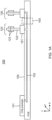
- FIG. 1A is an illustration of an example system 100, adapted according to one aspect useful for the understanding of the invention not corresponding to the claims.
- the example system 100 includes a chip package 101 coupled to PCB 104.
- Chip package 101 may include any appropriate processing device, such as a digital signal processor (DSP), a central processing unit (CPU), a system on chip (SOC) having multiple cores, and/or the like.
- DSP digital signal processor
- CPU central processing unit
- SOC system on chip
- Chip package 101 and the DIMM modules 120, 130 are electrically coupled to conductive traces 102 to carry signals between chip package 101 and the DIMM modules 120, 130.
- Printed circuit board 104 includes a plurality of layers of insulating material separating other layers of conductive material.
- the conductive material may include metals such as copper or copper alloys.
- the traces 102 are implemented in one layer in this example, although other embodiments may include multiple layers of metal interleaved with layers of insulating material.
- An example insulating material for a PCB includes FR-4 glass epoxy, although the scope of embodiments is not limited to any particular material for PCB 104.
- Figure 1A is an illustration of example system 100 shown from a side-on view of the X-Y plane.
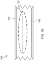
- Figure 1B complements Figure 1A by showing a portion of an end-on, cutaway view in the Y-Z plane.
- Figure 1B is not drawn to scale.
- PCB 104 in this example further includes a first conductive ground plane 105 parallel to the traces 102 and in a layer vertically above traces 102 as well as a second conductive ground plane 106 parallel to the traces 102 and vertically in a layer below traces 102.
- the ground planes 105, 106 would appear as lines in the view shown in Figure 1A .
- traces 102 are shown as a group of metal lines laid out in a layer of PCB 104.
- Traces 102 may include any number of independent lines, and in other examples, may include lines in other layers between the ground planes 105, 106. Examples of suitable ground plane material include copper, copper alloys, and the like. Traces 102 are physically separated from ground planes 105, 106 in Figure 1B by insulating layers.
- this example aspect includes EBG structure 103 which is placed between the DIMM modules 120, 130 to attenuate signals that would otherwise cause reflections.
- EBG structure 103 is shown in this example as a rectangle for simplicity, but it is understood that it may be implemented using any appropriate physical structure, such as slots in either or both of the ground planes, varying width portions of the traces, varying dielectric medium of the PCB 104, and/or the like.
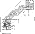
- FIG 2 is an illustration of an example PCB 200, which illustrates in more detail a particular physical implementation of PCB 104 of Figure 1A .
- Area 201 indicates where chip package 101 would be coupled to the PCB 104 of Figure 1 .
- the various holes (e.g., vias) provide electrical communication from pins of the chip package 101 to layers and structures within the PCB 200.
- the topmost ground plane 105 is eliminated from this view for ease of reference, and it is understood that the topmost ground plane 105 would be placed in a layer above traces 202.
- Traces 202 are conductive lines on one or more layers of the PCB 200, and they couple pins of the chip package 101 to pins of the DIMM modules.
- DIMM module 1 represents near DIMM module 120 of Figure 1
- DIMM module 0 represents far DIMM module 130 of Figure 1 .
- the DIMM modules are eliminated for ease of reference, and it is understood that the pins of the DIMM modules 1 and 0 would be coupled to PCB 200 and the traces 202 through holes such as holes 204.
- DIMM module 1 and DIMM module 0 are electrically coupled to the traces using the same channels, so that the chip package 101 communicates with only one of the DIMM modules at a given time.
- the traces 202 couple the DIMM module 0 and DIMM module 1 to the chip package in area 201 using a multi-drop bus architecture in which both DIMM modules couple to the same traces.
- Area 210 indicates a portion of the ground plane in which the EBG structure is implemented. As shown, the EBG structure has multiple rectangular slots cut into the bottommost ground plane. The pitch and width of each of the rectangular slots collectively determine the frequency band at which the EBG structure provides attenuation. Example slots are shown as 211 in this example.
- the rectangular slots of the EBG structure are arranged so that their length dimension is perpendicular to a length dimension of the traces 202, and the EBG structure underlies the area between the two DIMM modules as well as areas directly underneath each of the two DIMM modules.
- FIG 3 is an illustration of the example PCB 200, but with a different physical implementation of the EBG structure.
- area 310 indicates the area in which the EBG structure is located.
- the EBG structure includes varied width sections of each of the conductive traces 202 within area 310.
- An example of varied width sections include sections 311, which are wider than other portions of the same trace.
- the width and pitch of the varied width sections determines the frequency band at which the EBG structure provides attenuation.
- the aspect useful for the understanding of the invention not corresponding to the claims of Figure 3 implements the EBG structure on the conductive traces themselves.
- FIG 4 is another illustration of a PCB 200 according to an embodiment of the invention with yet another physical implementation of the EBG structure different from those shown above with respect to Figures 2 and 3 .
- Area 410 indicates the area in which the EBG structure is implemented.
- the EBG structure is implemented as a multitude of sinusoidal-shaped slots in the bottommost ground plane.
- An example of slots is shown at items 411. Further in this example, a length dimension of each of the sinusoidal-shaped slots is aligned parallel with the primary direction of the length dimension of traces 202.
- Figure 4 includes example sinusoidal-shaped slots 420 showing how two adjacent sinusoidal-shaped slots might appear under magnification.
- the frequency at which the EBG structure provides attenuation is determined by the period and amplitude of the shape of the sinusoid. Furthermore, other embodiments may use multiple sinusoids with different periods and shapes as appropriate.
- R is reflectance
- D is length of structure
- M Sinusoidal Modulation of dielectric constant
- k1 is wave number of periodic medium
- L is period of the periodic cell.
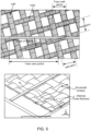
- Figure 5 is yet another illustration of a physical implementation of an EBG structure.
- Figure 5 shows a top-down view and a perspective view of a fiber weave in a layer of a PCB, such as PCB 104 of Figures 1A and 1B .
- Weaves' type and angle of rotation of trace with respect to weave may be configured to have a varying dielectric medium that provides desirable EBG properties.
- Dielectric laminate PCBs are commonly made of fiberglass strings woven as reinforcement for the resin medium.
- Woven fiberglass cloths may be configured to form a periodic medium with alternating fiberglass and resin regions. These periodic regions can be designed to form EBG structures in the PCB medium.
- band gap frequency and bandwidth can be controlled.
- one or more layers of fiber weave may be placed between traces 102 and ground plane 105 and/or between traces 102 and ground plane 106.
- One example includes selection of a weave type, such as with various widths of the wrap and weft. Another example is selection of resin and fiberglass dielectric constants. Yet another example includes angle of rotation of the routing with respect to the fiber weave orientation. Another example includes a cross-sectional shape (e.g., sinusoidal cross-section) of the fiber weave bundles. An engineer may simulate a PCB having various periodic medium geometries to find one or more geometries that provide desirable EBG properties.
- Various embodiments and examples may then be implemented using one or more layers in a PCB that include EBG structures to provide a desired amount of reflection attenuation.
- FIGS 2- 5 are provided to illustrate that EBG structures may take a variety of different physical implementations. Furthermore, while the examples of Figures 2 and 3 show slots in the bottommost ground plane, it is understood that slots may be implemented in the topmost ground plane or in both ground planes as appropriate. Furthermore, the EBG structures of the illustrated embodiments are located in different layers of the PCB than are the traces, and specifically, are located laterally (in the X-dimension in Figure 1A ) between the memory modules. However, the EBG structures may be scaled as appropriate so that they are not just laterally between the memory modules, but span into areas that laterally underlie either or both of the memory modules. In any event, EBG structures may be adapted for use in various embodiments to attenuate reflections in a multi-drop bus.
- Figure 6 is an illustration of four different example eye diagrams 602, 604, 612, 614, according to one embodiment.
- Figures 6-7 show numbers for margin, time, and voltage, and these numbers are for illustration only. Other embodiments may have different numbers for such parameters as appropriate.
- the eye diagrams 602, 604, 612, 614 show a time domain representation of multiple bit transitions overlaid on a same display. The diagrams of Figure 6 may be acquired through simulation or testing.
- diagram 612 shows a multitude of bit transitions, according to either a simulation or measurement, as they would occur at the near DIMM module (DIMM module 1).
- DIMM module DIMM module 1
- the tighter the lines in a given eye diagram the less variance there is between different transitions at different times. Greater variance may often be caused by inter-symbol interference, which itself may be the result of signal reflections.
- Eye diagram 614 illustrates bit transitions at the far DIMM module (DIMM module 0) according to either simulation or measurement. Both eye diagrams 612 and 614 represent behavior that would be expected with the embodiments shown in Figures 1-5 .
- the openness of the middle portion of the eye diagram illustrates a time available to capture a bit during a transition. For instance, a clock may sample data, so the clock edge would preferably be placed in the middle of the eye diagram, where the middle represents the highest binary 1 and the lowest binary 0. It is typically undesirable to sample too early or too late, as the bit may not be captured correctly.
- the larger the opening in the eye the more time is available to capture the bit.
- the more tightly the lines overlap in the eye diagram with less variance the more time there is available to capture the bit.
- the rectangles in the middle of eye diagrams 612, 614 is a JEDEC Solid State Technology Association specification, and it corresponds to a desired time to capture a bit.
- Margin refers to a time illustrated by the distance between a corner of the rectangle and the nearest line in the eye diagram. The smaller the margin, the less time there is available to capture the bit. Looking at eye diagrams 612 and 614, there is a margin of 47.92 ps and 58.25 ps, respectively. Such values may or may not be acceptable for a given application. However, these numbers are in contrast to the margins shown with respect to eye diagrams 602, 604.
- Eye diagrams 602, 604 correspond to a system similar to that shown in any of Figures 1-5 , but without the EBG structures to attenuate reflections. Eye diagrams 602, 604 show a margin of 12.50 ps and 97.92 ps, respectively.
- the addition of the EBG structures may attenuate reflections, but also attenuate the signal from the chip as well, thereby somewhat diminishing timing performance at the far DIMM module.
- the improved margin at the near DIMM module may move the timing performance of the near DIMM module from an unacceptable level to an acceptable level, depending on the particular application.
- some diminished performance at the far DIMM module may be an acceptable price to pay for increased performance at the near DIMM module, especially in applications where both of the DIMM modules fall within an acceptable level of margin.
- Figure 7 is an illustration of four example frequency diagrams 702, 704, 712, 714, according to one embodiment.
- Diagram 702, 704 are frequency domain diagrams that correspond to the eye diagrams 602, 604, respectively, of Figure 6 .
- diagrams 712, 714 are frequency domain diagrams that correspond to the eye diagrams 612, 614, respectively.
- Diagrams 702, 704, 712, 714 illustrate attenuation in the frequency bands from about 1.6 GHz to 3.3 GHz, which in some embodiments may be a fundamental frequency band of interest. For instance, some embodiments may use signals within that frequency band to transmit data from a chip to DIMM modules, as shown in Figure 1 .
- Diagrams 712, 714 show simulated performance using the EBG structures of Figure 2 .
- EBG structures of Figures 1-5 may provide acceptable timing performance for systems having two DIMM modules electrically coupled by a daisy chained stub without perceptible performance loss at either of the DIMM modules.
- inventions and examples shown in Figures 1-5 may provide acceptable performance even in applications when only one DIMM module is coupled to the PCB. This is in contrast to a conventional Tee topology, which would typically be expected to return poor results when only one DIMM module populates the board. Therefore, various embodiments described herein may include boards used for both single-DIMM module and dual-DIMM module applications as appropriate. In other words, other examples may include variations on the systems of Figures 1-5 , wherein only one of the memory module slots is populated (e.g., either the far slot or the near slot, but not both).
- boards having processors, at least one memory module, and an EBG structure may be employed in computing systems, such as servers, desktop computers, laptop computers, and the like.
- computing systems such as servers, desktop computers, laptop computers, and the like.
- the scope of embodiments is not limited thereto, as boards for use in mobile devices may be adapted according to the principles described herein.
- Figure 8 is an illustration of an example method 800 for designing a system having EBG structures, according to one aspect useful for the understanding of the invention not corresponding to the claims.
- Method 800 may be performed, for example, by an engineer using one or more simulation tools.
- an engineer determines the daisy chain geometry of the board and then simulates timing performance of one or both of the DIMM modules at the desired frequency band.
- the engineer determines whether the desired frequency band, the fundamental frequency, is affected. For instance, at actions 802-804, the engineer may simulate the design using time domain and/or frequency domain techniques to determine whether timing performance is diminished in the desired frequency band. If the desired frequency band is affected at action 804, then method 800 moves to action 806. Otherwise, the inquiry may stop.
- action 806 the engineer determines periodic geometry type and calculates dimensions using approximate equations.
- action 806 includes coming up with best guess dimensions for EBG structures. For instance, best guess may include pitch and width ( Figures 2 and 3 ) or sinusoidal frequency and amplitude ( Figure 4 ), or other parameter for an appropriate EBG structure.
- Action 806 may include using equations, such as those discussed above with respect to Figures 2 and 4 to initially set parameters.
- the engineer models the calculated EBG structures in a three dimensional electromagnetic field solver program. The modeling produces information similar to that of Figures 6 and 7 , allowing the engineer to determine frequency gain and timing performance for the structures.
- the engineer optimizes the structures by sweeping the parameters around calculated nominal values. For instance, the engineer may change pitch, width, sinusoidal frequency, amplitude of a structure and perform the modeling of action 808 to further refine the shape and enhance performance. Action 810 may be iterative with redesign and modeling.
- Action 812 includes verifying the effectiveness of the solution in time domain simulations.
- Example time domain simulations include eye diagrams and may further include analyzing timing margin and noise margin. If the solution is not effective, the method 800 may return to action 810 to further enhance the design until it is acceptable.
- Figure 9 is an illustration of an example plot of results during the actions 810 and 812, where an engineer may simulate designs to test margins for both a near DIMM and a far DIMM. In the example of Figure 8 , a solution is where performance of the near DIMM and the far DIMM margins are substantially similar and are within an acceptable range for the application.
- Figure 10 illustrates an example method 1000, for use of the systems of Figures 1-5 .
- the actions of method 1000 may be performed, for example, by a computing apparatus, such as that shown in Figure 1A , having a chip package in electrical communication with two memory modules.
- a computing apparatus such as that shown in Figure 1A
- An example may include normal operation of a server or other computer including a board adapted according to the principles described herein.
- action 1010 includes propagating an electrical signal from a processing device on a PCB to a first memory module and a second memory module in electrical communication with a plurality of metal traces and sharing channels of the metal traces.
- the processing device may include, e.g., a central processing unit (CPU), digital signal processor (DSP), graphics processing unit (GPU) or other appropriate processing unit.
- the processing device performs operations including writing data to the memory modules and reading data from the memory modules.
- the memory modules themselves store data and access data in response to commands from the processing device.
- Propagating electrical signals may be performed by electrical traces, such as those illustrated in Figures 1-4 .
- metal traces may be configured as a multi-drop bus so that each of the memory modules are physically and electrically coupled with the same ones of the traces.
- action 1010 may include the electrical signal propagating along the bus, though any particular instruction or data may be addressed to only a given one of the memory modules.
- Action 1020 includes attenuating reflections of the electrical signal at an EBG structure.
- the EBG structure may be physically disposed in an area between the first memory module and the second memory module. Different physical placements are shown and discussed above with respect to Figures 1-4 .
- aspects is not limited to the actions shown in Figure 10 .
- other aspects may add, omit, rearrange, or modify one or more the actions.
- a board is populated similarly to that of Figure 1A , except that only one of the memory modules is populated on the board.
- propagating electrical signals may be performed with respect to only that single memory module.
- embodiments and examples having three or more memory modules may include propagating electrical signals to each one of those memory modules.
- the actions 1010 and 1020 may be repeated continuously throughout operation of the device.
- the EBG structure may thus provide attenuation of electromagnetic reflection, and in some instances provide increased performance of the device.
Landscapes
- Engineering & Computer Science (AREA)
- Microelectronics & Electronic Packaging (AREA)
- Physics & Mathematics (AREA)
- Computer Hardware Design (AREA)
- General Physics & Mathematics (AREA)
- Electromagnetism (AREA)
- General Engineering & Computer Science (AREA)
- Theoretical Computer Science (AREA)
- Condensed Matter Physics & Semiconductors (AREA)
- Power Engineering (AREA)
- Geometry (AREA)
- Structure Of Printed Boards (AREA)
Applications Claiming Priority (3)
| Application Number | Priority Date | Filing Date | Title |
|---|---|---|---|
| US201662367836P | 2016-07-28 | 2016-07-28 | |
| US15/659,187 US10349513B2 (en) | 2016-07-28 | 2017-07-25 | Circuits and methods providing electronic band gap (EBG) structures at memory module electrical coupling |
| PCT/US2017/043844 WO2018022687A1 (en) | 2016-07-28 | 2017-07-26 | Circuits and methods providing electronic band gap (ebg) structures at memory module electrical coupling |
Publications (3)
| Publication Number | Publication Date |
|---|---|
| EP3491898A1 EP3491898A1 (en) | 2019-06-05 |
| EP3491898C0 EP3491898C0 (en) | 2024-09-25 |
| EP3491898B1 true EP3491898B1 (en) | 2024-09-25 |
Family
ID=61010581
Family Applications (1)
| Application Number | Title | Priority Date | Filing Date |
|---|---|---|---|
| EP17754863.3A Active EP3491898B1 (en) | 2016-07-28 | 2017-07-26 | Circuits and methods providing electronic band gap (ebg) structures at memory module electrical coupling |
Country Status (9)
| Country | Link |
|---|---|
| US (1) | US10349513B2 (enExample) |
| EP (1) | EP3491898B1 (enExample) |
| JP (1) | JP6633243B2 (enExample) |
| KR (1) | KR102078065B1 (enExample) |
| CN (1) | CN109565925B (enExample) |
| AU (1) | AU2017302566B9 (enExample) |
| BR (1) | BR112019001333B1 (enExample) |
| TW (1) | TWI695658B (enExample) |
| WO (1) | WO2018022687A1 (enExample) |
Families Citing this family (3)
| Publication number | Priority date | Publication date | Assignee | Title |
|---|---|---|---|---|
| US11169940B2 (en) * | 2019-02-20 | 2021-11-09 | Qualcomm Incorporated | Trace length on printed circuit board (PCB) based on input/output (I/O) operating speed |
| TWI795644B (zh) * | 2020-06-02 | 2023-03-11 | 大陸商上海兆芯集成電路有限公司 | 電子總成 |
| JP7529628B2 (ja) * | 2021-07-26 | 2024-08-06 | 株式会社日立製作所 | プリント配線板及び情報処理装置 |
Citations (2)
| Publication number | Priority date | Publication date | Assignee | Title |
|---|---|---|---|---|
| US20080176471A1 (en) * | 2007-01-05 | 2008-07-24 | Hitachi, Ltd. | Glass cloth wiring substrate |
| US20120274423A1 (en) * | 2010-12-03 | 2012-11-01 | Murata Manufacturing Co., Ltd. | High-frequency signal transmission line |
Family Cites Families (24)
| Publication number | Priority date | Publication date | Assignee | Title |
|---|---|---|---|---|
| US3876964A (en) | 1973-08-23 | 1975-04-08 | Amp Inc | Flat flexible transmission cable |
| JP3307597B2 (ja) | 1998-09-30 | 2002-07-24 | 株式会社 アドテック | 印刷配線装置 |
| JP4023166B2 (ja) | 2002-01-25 | 2007-12-19 | ソニー株式会社 | 高周波モジュール用基板及び高周波モジュール |
| WO2006052133A2 (en) * | 2004-11-12 | 2006-05-18 | Doorzand Airdrive B.V. | Composition for cold preservation and perfusion of organs |
| KR20070062633A (ko) * | 2005-12-13 | 2007-06-18 | 삼성전자주식회사 | 컴퓨터 시스템의 시스템 기판에 장착되는 인터페이스 소켓장치 |
| JP2007228222A (ja) * | 2006-02-23 | 2007-09-06 | Mitsubishi Electric Corp | Ebgマテリアル |
| KR101265245B1 (ko) | 2006-11-01 | 2013-05-16 | 에이전시 포 사이언스, 테크놀로지 앤드 리서치 | 이중적층형 ebg 구조체 |
| ITRA20060064A1 (it) * | 2006-11-03 | 2008-05-04 | Fondazione Torino Wireless | Dispositivo con costante dielettrica modulata per la propagazione di onde elettromagnetiche. |
| US7768297B2 (en) | 2007-01-31 | 2010-08-03 | Rambus, Inc. | Multi-drop bus system |
| US7839654B2 (en) | 2007-02-28 | 2010-11-23 | International Business Machines Corporation | Method for ultimate noise isolation in high-speed digital systems on packages and printed circuit boards (PCBS) |
| US8164006B2 (en) * | 2008-03-19 | 2012-04-24 | Samsung Electro-Mechanics Co., Ltd. | Electromagnetic bandgap structure and printed circuit board |
| KR100956891B1 (ko) * | 2008-03-19 | 2010-05-11 | 삼성전기주식회사 | 전자기 밴드갭 구조물 및 인쇄회로기판 |
| KR101086856B1 (ko) * | 2008-04-16 | 2011-11-25 | 주식회사 하이닉스반도체 | 반도체 집적 회로 모듈 및 이를 구비하는 pcb 장치 |
| KR101038236B1 (ko) * | 2009-09-16 | 2011-06-01 | 삼성전기주식회사 | 전자기 밴드갭 구조를 구비하는 인쇄회로기판 |
| JP2011108123A (ja) * | 2009-11-20 | 2011-06-02 | Elpida Memory Inc | 終端基板、メモリシステム及びその反射波抑制方法 |
| US9112272B2 (en) * | 2010-08-12 | 2015-08-18 | Feinics Amatech Teoranta | Antenna modules for dual interface smart cards, booster antenna configurations, and methods |
| JP2013232613A (ja) * | 2012-04-05 | 2013-11-14 | Sony Corp | 配線基板及び電子機器 |
| JP5694251B2 (ja) | 2012-07-27 | 2015-04-01 | 株式会社東芝 | Ebg構造体および回路基板 |
| JP5670392B2 (ja) * | 2012-07-27 | 2015-02-18 | 株式会社東芝 | 回路基板 |
| JP6125274B2 (ja) * | 2013-02-27 | 2017-05-10 | 株式会社東芝 | 電子回路および電子機器 |
| US9858181B2 (en) * | 2013-06-20 | 2018-01-02 | Hitachi, Ltd. | Memory module having different types of memory mounted together thereon, and information processing device having memory module mounted therein |
| JP6168943B2 (ja) * | 2013-09-20 | 2017-07-26 | 株式会社東芝 | Ebg構造体、半導体デバイスおよび回路基板 |
| JP5690428B1 (ja) * | 2014-05-21 | 2015-03-25 | 株式会社フジクラ | プリント配線板 |
| WO2017037957A1 (en) | 2015-08-31 | 2017-03-09 | Hitachi, Ltd. | Information processing device, apparatus and connection wiring board |
-
2017
- 2017-07-25 US US15/659,187 patent/US10349513B2/en active Active
- 2017-07-26 BR BR112019001333-4A patent/BR112019001333B1/pt active IP Right Grant
- 2017-07-26 KR KR1020197002434A patent/KR102078065B1/ko active Active
- 2017-07-26 CN CN201780046093.3A patent/CN109565925B/zh active Active
- 2017-07-26 JP JP2019504126A patent/JP6633243B2/ja active Active
- 2017-07-26 AU AU2017302566A patent/AU2017302566B9/en active Active
- 2017-07-26 EP EP17754863.3A patent/EP3491898B1/en active Active
- 2017-07-26 WO PCT/US2017/043844 patent/WO2018022687A1/en not_active Ceased
- 2017-07-27 TW TW106125251A patent/TWI695658B/zh active
Patent Citations (2)
| Publication number | Priority date | Publication date | Assignee | Title |
|---|---|---|---|---|
| US20080176471A1 (en) * | 2007-01-05 | 2008-07-24 | Hitachi, Ltd. | Glass cloth wiring substrate |
| US20120274423A1 (en) * | 2010-12-03 | 2012-11-01 | Murata Manufacturing Co., Ltd. | High-frequency signal transmission line |
Also Published As
| Publication number | Publication date |
|---|---|
| AU2017302566B2 (en) | 2020-08-27 |
| TWI695658B (zh) | 2020-06-01 |
| BR112019001333B1 (pt) | 2024-01-02 |
| AU2017302566B9 (en) | 2020-12-24 |
| EP3491898C0 (en) | 2024-09-25 |
| TW201804885A (zh) | 2018-02-01 |
| US20180035533A1 (en) | 2018-02-01 |
| US10349513B2 (en) | 2019-07-09 |
| JP6633243B2 (ja) | 2020-01-22 |
| EP3491898A1 (en) | 2019-06-05 |
| AU2017302566A1 (en) | 2019-01-17 |
| JP2019525472A (ja) | 2019-09-05 |
| BR112019001333A2 (pt) | 2019-05-07 |
| WO2018022687A1 (en) | 2018-02-01 |
| CN109565925A (zh) | 2019-04-02 |
| CN109565925B (zh) | 2022-01-18 |
| KR102078065B1 (ko) | 2020-02-17 |
| KR20190029613A (ko) | 2019-03-20 |
Similar Documents
| Publication | Publication Date | Title |
|---|---|---|
| CN104041200B (zh) | 具有用于较高带宽传输的嵌入式电光无源元件的印刷电路板 | |
| US7435912B1 (en) | Tailoring via impedance on a circuit board | |
| US9515031B2 (en) | Mitigation of far-end crosstalk induced by routing and out-of-plane interconnects | |
| US7459638B2 (en) | Absorbing boundary for a multi-layer circuit board structure | |
| CN105307390A (zh) | 一种pcb板结构 | |
| US7459985B2 (en) | Connector having a cut-out for reduced crosstalk between differential conductors | |
| US9627787B2 (en) | DIMM connector region vias and routing | |
| EP3491898B1 (en) | Circuits and methods providing electronic band gap (ebg) structures at memory module electrical coupling | |
| US12101875B2 (en) | Double stub transmission line for suppression of harmonics | |
| CN208336463U (zh) | 一种共面波导传输线 | |
| US8669830B2 (en) | Method and device for routing over a void for high speed signal routing in electronic systems | |
| Kong et al. | Guided Interconnect-The Next-Generation Flex Circuits for High-Performance System Design | |
| Scogna | Signal integrity analysis of a 26 layers board with emphasis on the effect of non-functional pads | |
| CN101594738B (zh) | 信号导通元件 | |
| JP4343145B2 (ja) | 配線基板 | |
| CN117528929A (zh) | 400g自环光模块pcb的设计方法和pcb板 | |
| Archambeault et al. | Measurements and simulations for ground-to-ground plane noise DDR RAM daughter cards and motherboards for EMI emissions | |
| CN119726275A (zh) | 板线转接结构、高速连接装置及车机系统 | |
| JP2004355063A (ja) | 方向性結合器基板を用いたバスシステム | |
| Liao et al. | Challenges of high-speed channel design on GPU accelerated system | |
| Pan et al. | Stitching a reference plane split using routing layer traces to improve I/O bus signal integrity |
Legal Events
| Date | Code | Title | Description |
|---|---|---|---|
| STAA | Information on the status of an ep patent application or granted ep patent |
Free format text: STATUS: UNKNOWN |
|
| STAA | Information on the status of an ep patent application or granted ep patent |
Free format text: STATUS: THE INTERNATIONAL PUBLICATION HAS BEEN MADE |
|
| PUAI | Public reference made under article 153(3) epc to a published international application that has entered the european phase |
Free format text: ORIGINAL CODE: 0009012 |
|
| STAA | Information on the status of an ep patent application or granted ep patent |
Free format text: STATUS: REQUEST FOR EXAMINATION WAS MADE |
|
| 17P | Request for examination filed |
Effective date: 20181217 |
|
| AK | Designated contracting states |
Kind code of ref document: A1 Designated state(s): AL AT BE BG CH CY CZ DE DK EE ES FI FR GB GR HR HU IE IS IT LI LT LU LV MC MK MT NL NO PL PT RO RS SE SI SK SM TR |
|
| AX | Request for extension of the european patent |
Extension state: BA ME |
|
| DAV | Request for validation of the european patent (deleted) | ||
| DAX | Request for extension of the european patent (deleted) | ||
| STAA | Information on the status of an ep patent application or granted ep patent |
Free format text: STATUS: EXAMINATION IS IN PROGRESS |
|
| 17Q | First examination report despatched |
Effective date: 20210615 |
|
| GRAP | Despatch of communication of intention to grant a patent |
Free format text: ORIGINAL CODE: EPIDOSNIGR1 |
|
| STAA | Information on the status of an ep patent application or granted ep patent |
Free format text: STATUS: GRANT OF PATENT IS INTENDED |
|
| INTG | Intention to grant announced |
Effective date: 20240419 |
|
| GRAS | Grant fee paid |
Free format text: ORIGINAL CODE: EPIDOSNIGR3 |
|
| GRAA | (expected) grant |
Free format text: ORIGINAL CODE: 0009210 |
|
| STAA | Information on the status of an ep patent application or granted ep patent |
Free format text: STATUS: THE PATENT HAS BEEN GRANTED |
|
| AK | Designated contracting states |
Kind code of ref document: B1 Designated state(s): AL AT BE BG CH CY CZ DE DK EE ES FI FR GB GR HR HU IE IS IT LI LT LU LV MC MK MT NL NO PL PT RO RS SE SI SK SM TR |
|
| REG | Reference to a national code |
Ref country code: GB Ref legal event code: FG4D |
|
| REG | Reference to a national code |
Ref country code: CH Ref legal event code: EP |
|
| REG | Reference to a national code |
Ref country code: DE Ref legal event code: R096 Ref document number: 602017085063 Country of ref document: DE |
|
| REG | Reference to a national code |
Ref country code: IE Ref legal event code: FG4D |
|
| U01 | Request for unitary effect filed |
Effective date: 20241004 |
|
| U07 | Unitary effect registered |
Designated state(s): AT BE BG DE DK EE FI FR IT LT LU LV MT NL PT RO SE SI Effective date: 20241028 |
|
| PG25 | Lapsed in a contracting state [announced via postgrant information from national office to epo] |
Ref country code: NO Free format text: LAPSE BECAUSE OF FAILURE TO SUBMIT A TRANSLATION OF THE DESCRIPTION OR TO PAY THE FEE WITHIN THE PRESCRIBED TIME-LIMIT Effective date: 20241225 |
|
| PG25 | Lapsed in a contracting state [announced via postgrant information from national office to epo] |
Ref country code: GR Free format text: LAPSE BECAUSE OF FAILURE TO SUBMIT A TRANSLATION OF THE DESCRIPTION OR TO PAY THE FEE WITHIN THE PRESCRIBED TIME-LIMIT Effective date: 20241226 |
|
| PG25 | Lapsed in a contracting state [announced via postgrant information from national office to epo] |
Ref country code: RS Free format text: LAPSE BECAUSE OF FAILURE TO SUBMIT A TRANSLATION OF THE DESCRIPTION OR TO PAY THE FEE WITHIN THE PRESCRIBED TIME-LIMIT Effective date: 20241225 |
|
| PG25 | Lapsed in a contracting state [announced via postgrant information from national office to epo] |
Ref country code: RS Free format text: LAPSE BECAUSE OF FAILURE TO SUBMIT A TRANSLATION OF THE DESCRIPTION OR TO PAY THE FEE WITHIN THE PRESCRIBED TIME-LIMIT Effective date: 20241225 Ref country code: NO Free format text: LAPSE BECAUSE OF FAILURE TO SUBMIT A TRANSLATION OF THE DESCRIPTION OR TO PAY THE FEE WITHIN THE PRESCRIBED TIME-LIMIT Effective date: 20241225 Ref country code: GR Free format text: LAPSE BECAUSE OF FAILURE TO SUBMIT A TRANSLATION OF THE DESCRIPTION OR TO PAY THE FEE WITHIN THE PRESCRIBED TIME-LIMIT Effective date: 20241226 |
|
| PG25 | Lapsed in a contracting state [announced via postgrant information from national office to epo] |
Ref country code: IS Free format text: LAPSE BECAUSE OF FAILURE TO SUBMIT A TRANSLATION OF THE DESCRIPTION OR TO PAY THE FEE WITHIN THE PRESCRIBED TIME-LIMIT Effective date: 20250125 |
|
| PG25 | Lapsed in a contracting state [announced via postgrant information from national office to epo] |
Ref country code: SM Free format text: LAPSE BECAUSE OF FAILURE TO SUBMIT A TRANSLATION OF THE DESCRIPTION OR TO PAY THE FEE WITHIN THE PRESCRIBED TIME-LIMIT Effective date: 20240925 |
|
| PG25 | Lapsed in a contracting state [announced via postgrant information from national office to epo] |
Ref country code: ES Free format text: LAPSE BECAUSE OF FAILURE TO SUBMIT A TRANSLATION OF THE DESCRIPTION OR TO PAY THE FEE WITHIN THE PRESCRIBED TIME-LIMIT Effective date: 20240925 |
|
| PG25 | Lapsed in a contracting state [announced via postgrant information from national office to epo] |
Ref country code: CZ Free format text: LAPSE BECAUSE OF FAILURE TO SUBMIT A TRANSLATION OF THE DESCRIPTION OR TO PAY THE FEE WITHIN THE PRESCRIBED TIME-LIMIT Effective date: 20240925 Ref country code: PL Free format text: LAPSE BECAUSE OF FAILURE TO SUBMIT A TRANSLATION OF THE DESCRIPTION OR TO PAY THE FEE WITHIN THE PRESCRIBED TIME-LIMIT Effective date: 20240925 |
|
| PG25 | Lapsed in a contracting state [announced via postgrant information from national office to epo] |
Ref country code: SK Free format text: LAPSE BECAUSE OF FAILURE TO SUBMIT A TRANSLATION OF THE DESCRIPTION OR TO PAY THE FEE WITHIN THE PRESCRIBED TIME-LIMIT Effective date: 20240925 |
|
| PGFP | Annual fee paid to national office [announced via postgrant information from national office to epo] |
Ref country code: GB Payment date: 20250612 Year of fee payment: 9 |
|
| U20 | Renewal fee for the european patent with unitary effect paid |
Year of fee payment: 9 Effective date: 20250617 |
|
| PGFP | Annual fee paid to national office [announced via postgrant information from national office to epo] |
Ref country code: IE Payment date: 20250612 Year of fee payment: 9 |
|
| PLBE | No opposition filed within time limit |
Free format text: ORIGINAL CODE: 0009261 |
|
| STAA | Information on the status of an ep patent application or granted ep patent |
Free format text: STATUS: NO OPPOSITION FILED WITHIN TIME LIMIT |
|
| 26N | No opposition filed |
Effective date: 20250626 |