EP3489990B1 - Semiconductor substrate - Google Patents
Semiconductor substrate Download PDFInfo
- Publication number
- EP3489990B1 EP3489990B1 EP17830936.5A EP17830936A EP3489990B1 EP 3489990 B1 EP3489990 B1 EP 3489990B1 EP 17830936 A EP17830936 A EP 17830936A EP 3489990 B1 EP3489990 B1 EP 3489990B1
- Authority
- EP
- European Patent Office
- Prior art keywords
- sic
- interface
- nitrogen
- atoms
- layer
- Prior art date
- Legal status (The legal status is an assumption and is not a legal conclusion. Google has not performed a legal analysis and makes no representation as to the accuracy of the status listed.)
- Active
Links
Images


Classifications
-
- H—ELECTRICITY
- H01—ELECTRIC ELEMENTS
- H01L—SEMICONDUCTOR DEVICES NOT COVERED BY CLASS H10
- H01L21/00—Processes or apparatus adapted for the manufacture or treatment of semiconductor or solid state devices or of parts thereof
- H01L21/02—Manufacture or treatment of semiconductor devices or of parts thereof
- H01L21/04—Manufacture or treatment of semiconductor devices or of parts thereof the devices having potential barriers, e.g. a PN junction, depletion layer or carrier concentration layer
- H01L21/18—Manufacture or treatment of semiconductor devices or of parts thereof the devices having potential barriers, e.g. a PN junction, depletion layer or carrier concentration layer the devices having semiconductor bodies comprising elements of Group IV of the Periodic Table or AIIIBV compounds with or without impurities, e.g. doping materials
- H01L21/185—Joining of semiconductor bodies for junction formation
- H01L21/187—Joining of semiconductor bodies for junction formation by direct bonding
-
- H—ELECTRICITY
- H01—ELECTRIC ELEMENTS
- H01L—SEMICONDUCTOR DEVICES NOT COVERED BY CLASS H10
- H01L21/00—Processes or apparatus adapted for the manufacture or treatment of semiconductor or solid state devices or of parts thereof
- H01L21/02—Manufacture or treatment of semiconductor devices or of parts thereof
- H01L21/04—Manufacture or treatment of semiconductor devices or of parts thereof the devices having potential barriers, e.g. a PN junction, depletion layer or carrier concentration layer
- H01L21/18—Manufacture or treatment of semiconductor devices or of parts thereof the devices having potential barriers, e.g. a PN junction, depletion layer or carrier concentration layer the devices having semiconductor bodies comprising elements of Group IV of the Periodic Table or AIIIBV compounds with or without impurities, e.g. doping materials
- H01L21/185—Joining of semiconductor bodies for junction formation
-
- H—ELECTRICITY
- H10—SEMICONDUCTOR DEVICES; ELECTRIC SOLID-STATE DEVICES NOT OTHERWISE PROVIDED FOR
- H10D—INORGANIC ELECTRIC SEMICONDUCTOR DEVICES
- H10D62/00—Semiconductor bodies, or regions thereof, of devices having potential barriers
- H10D62/80—Semiconductor bodies, or regions thereof, of devices having potential barriers characterised by the materials
- H10D62/83—Semiconductor bodies, or regions thereof, of devices having potential barriers characterised by the materials being Group IV materials, e.g. B-doped Si or undoped Ge
- H10D62/832—Semiconductor bodies, or regions thereof, of devices having potential barriers characterised by the materials being Group IV materials, e.g. B-doped Si or undoped Ge being Group IV materials comprising two or more elements, e.g. SiGe
- H10D62/8325—Silicon carbide
-
- H—ELECTRICITY
- H01—ELECTRIC ELEMENTS
- H01L—SEMICONDUCTOR DEVICES NOT COVERED BY CLASS H10
- H01L21/00—Processes or apparatus adapted for the manufacture or treatment of semiconductor or solid state devices or of parts thereof
- H01L21/02—Manufacture or treatment of semiconductor devices or of parts thereof
- H01L21/02002—Preparing wafers
-
- H—ELECTRICITY
- H01—ELECTRIC ELEMENTS
- H01L—SEMICONDUCTOR DEVICES NOT COVERED BY CLASS H10
- H01L21/00—Processes or apparatus adapted for the manufacture or treatment of semiconductor or solid state devices or of parts thereof
- H01L21/02—Manufacture or treatment of semiconductor devices or of parts thereof
- H01L21/02104—Forming layers
- H01L21/02365—Forming inorganic semiconducting materials on a substrate
- H01L21/02367—Substrates
- H01L21/0237—Materials
- H01L21/02373—Group 14 semiconducting materials
- H01L21/02378—Silicon carbide
-
- H—ELECTRICITY
- H01—ELECTRIC ELEMENTS
- H01L—SEMICONDUCTOR DEVICES NOT COVERED BY CLASS H10
- H01L21/00—Processes or apparatus adapted for the manufacture or treatment of semiconductor or solid state devices or of parts thereof
- H01L21/02—Manufacture or treatment of semiconductor devices or of parts thereof
- H01L21/02104—Forming layers
- H01L21/02365—Forming inorganic semiconducting materials on a substrate
- H01L21/02518—Deposited layers
- H01L21/02587—Structure
- H01L21/0259—Microstructure
- H01L21/02595—Microstructure polycrystalline
-
- H—ELECTRICITY
- H01—ELECTRIC ELEMENTS
- H01L—SEMICONDUCTOR DEVICES NOT COVERED BY CLASS H10
- H01L21/00—Processes or apparatus adapted for the manufacture or treatment of semiconductor or solid state devices or of parts thereof
- H01L21/02—Manufacture or treatment of semiconductor devices or of parts thereof
- H01L21/02104—Forming layers
- H01L21/02365—Forming inorganic semiconducting materials on a substrate
- H01L21/02518—Deposited layers
- H01L21/02587—Structure
- H01L21/0259—Microstructure
- H01L21/02598—Microstructure monocrystalline
-
- H—ELECTRICITY
- H10—SEMICONDUCTOR DEVICES; ELECTRIC SOLID-STATE DEVICES NOT OTHERWISE PROVIDED FOR
- H10D—INORGANIC ELECTRIC SEMICONDUCTOR DEVICES
- H10D62/00—Semiconductor bodies, or regions thereof, of devices having potential barriers
- H10D62/40—Crystalline structures
-
- H—ELECTRICITY
- H01—ELECTRIC ELEMENTS
- H01L—SEMICONDUCTOR DEVICES NOT COVERED BY CLASS H10
- H01L2924/00—Indexing scheme for arrangements or methods for connecting or disconnecting semiconductor or solid-state bodies as covered by H01L24/00
- H01L2924/01—Chemical elements
- H01L2924/01006—Carbon [C]
-
- H—ELECTRICITY
- H01—ELECTRIC ELEMENTS
- H01L—SEMICONDUCTOR DEVICES NOT COVERED BY CLASS H10
- H01L2924/00—Indexing scheme for arrangements or methods for connecting or disconnecting semiconductor or solid-state bodies as covered by H01L24/00
- H01L2924/01—Chemical elements
- H01L2924/01007—Nitrogen [N]
-
- H—ELECTRICITY
- H01—ELECTRIC ELEMENTS
- H01L—SEMICONDUCTOR DEVICES NOT COVERED BY CLASS H10
- H01L2924/00—Indexing scheme for arrangements or methods for connecting or disconnecting semiconductor or solid-state bodies as covered by H01L24/00
- H01L2924/01—Chemical elements
- H01L2924/01014—Silicon [Si]
-
- H—ELECTRICITY
- H01—ELECTRIC ELEMENTS
- H01L—SEMICONDUCTOR DEVICES NOT COVERED BY CLASS H10
- H01L2924/00—Indexing scheme for arrangements or methods for connecting or disconnecting semiconductor or solid-state bodies as covered by H01L24/00
- H01L2924/01—Chemical elements
- H01L2924/01015—Phosphorus [P]
Definitions
- the description herein discloses a technique related to a bonded semiconductor substrate capable of reducing an interface resistance.
- WO 2016/006663 A1 discloses a semiconductor substrate comprising a single-crystalline SiC substrate and a polycrystalline SiC substrate, wherein the single-crystalline SiC substrate and the polycrystalline SiC substrate are bonded via an interface layer, and the interface layer is a composite material containing carbon and silicon.
- the present disclosure provides a semiconductor substrate in accordance with claim 1.
- the semiconductor substrate comprises a single-crystalline SiC substrate and a polycrystalline SiC substrate.
- the single-crystalline SiC substrate and the polycrystalline SiC substrate are bonded via an interface layer.
- the interface layer is a composite material containing carbon and silicon.
- a bonded region of the single-crystalline SiC substrate and the polycrystalline SiC substrate/ the interface layer contains 1 ⁇ 10 21 atoms/cm 3 or more of nitrogen atoms.
- the single-crystalline SiC substrate and the polycrystalline SiC substrate are bonded directly, a potential barrier is generated, by which an interface resistance becomes high.
- the single-crystalline SiC substrate and the polycrystalline SiC substrate are bonded. Since a potential barrier is generated at a bonded interface of the single-crystalline SiC substrate and the polycrystalline SiC substrate, an interface resistance component thereby exists.
- the interface resistance can be suppressed by having the nitrogen atoms contained at 1 ⁇ 10 21 atoms/cm 3 or more.
- a technique that improves an electric characteristic of a semiconductor substrate having a single-crystalline SiC substrate and a polycrystalline SiC substrate bonded can be provided.
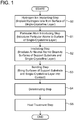
- FIG. 1 is a flowchart showing a method of manufacturing a bonded substrate
- FIG. 2 is a perspective view of the bonded substrate
- FIG. 3 is a schematic view of the bonded substrate
- FIG. 4 is a schematic view of the bonded substrate
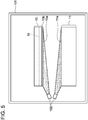
- FIG. 5 is an explanatory diagram of an irradiation step of the bonded substrate
- FIG. 6 is a schematic view of the bonded substrate
- FIG. 7 is a schematic view of the bonded substrate
- FIG. 8 is a schematic view of the bonded substrate
- FIG. 9 is a graph showing a relationship between an introduced amount of nitrogen and an interface resistance
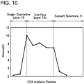
- FIG. 10 is a graph showing a nitrogen density profile of an interface
- FIG. 11 is a diagram showing an electrogenesis mechanism model
- FIG. 12 is a diagram showing an electrogenesis mechanism model.
- the nitrogen atoms may alter at least a part of a SiC crystal structure in the bonded region when the nitrogen atoms are present in the bonded region at a density of 1 ⁇ 10 21 atoms/cm 3 or more.
- a thickness of the interface layer may be equal to or more than 0.25 nanometer.
- the interface layer may contain 1 ⁇ 10 22 atoms/cm 3 or more of the nitrogen atoms
- a ratio of the nitrogen atoms may be 10 atomic% or more.
- the single-crystalline SiC substrate may be 4H-SiC.
- the polycrystalline SiC substrate may be 3C-SiC.
- FIG. 2 is a perspective view of a bonded substrate 10 according to the present embodiment.
- the bonded substrate 10 has an approximately disc-like shape.
- the bonded substrate 10 includes a support substrate 11 disposed on the underside, and a single-crystalline layer 13 bonded to the upper surface of the support substrate 11.
- the single-crystalline layer 13 is formed from single-crystalline SiC, for example, single crystals of a compound semiconductor (e.g., 6H-SiC, 4H-SiC).
- the support substrate 11 is resistant to various thermal processes applied to the single-crystalline layer 13. Additionally, it is preferable that the support substrate 11 is formed from a material with a small difference in thermal expansion coefficient between the single-crystalline layer 13 and this substrate 11. For example, if SiC is used for the single-crystalline layer 13, polycrystalline SiC is used for the support substrate 11. In the polycrystalline SiC, various poly-types and crystal face of SiC crystal may be mixed. Polycrystalline SiC in which various poly-types and crystal face are mixed can be manufactured without severe temperature control, thus it can enable a reduction in the manufacturing cost of the support substrate 11.
- Thickness TT1 of the support substrate 11 needs to be set so as to obtain mechanical strength, which is able to withstand post-processing of semiconductor device manufacturing. For example, if the diameter of the support substrate 11 is 150 mm, the thickness TT1 may be about 350 micrometer.
- a method of manufacturing the bonded substrate 10 according to the present embodiment will be described with reference to FIGS. 1 to 8 .
- the support substrate 11 is polycrystalline 3C-SiC and the single-crystalline layer 13 is single-crystalline 4H-SiC will be described.
- the manufacturing flow described herein is implemented by using delamination technique by hydrogen atom ablation will be described.
- the support substrate 11 and the single-crystalline layer 13 are prepared.
- the support substrate 11 and the single-crystalline layer 13 have planarized surfaces.
- the planarization may be performed by polishing or cutting or may be performed by a CMP method.
- a hydrogen ion implanting step of implanting hydrogen ions from a front surface 13a of the single-crystalline layer 13 is performed.
- the hydrogen ions When the hydrogen ions are implanted in the single-crystalline layer 13, the hydrogen ions reach depths corresponding to their incident energy, and are distributed in high density. Due to this, as shown in a schematic view of FIG. 3 , a hydrogen implanted layer 15 is formed at a predetermined depth from the front surface. In the present embodiment, a case will be described in which the hydrogen implanted layer 15 is formed at a position at about 0.5 micrometer from the front surface.
- a particular atom introducing step is performed.
- Particular atoms may be any atoms so long as they can alter a crystal structure of the single-crystalline layer 13.
- a configuration in which "the crystal structure of the single-crystalline layer 13 is altered" includes various types of configurations. For example, a configuration in which the crystal structure is altered by generating a large quantity of crystal defects is included. Further, a configuration in which the crystal structure itself is altered to a structure that is different from its structure before introduction of the particular atoms is included. Further, a configuration in which the single-crystalline layer 13 is amorphized is included. Further, a configuration in which a compound other than SiC is formed is included. Further, a configuration in which some sort of element is precipitated is included. Such configurations are mere examples. They do not exclude configurations other than the above.
- the particular atoms may be atoms that bonds with Si and C.
- at least nitrogen (N) may be exemplified.
- N nitrogen
- Neutral atomic beam of nitrogen is irradiated to the front surface 13a of the single-crystalline layer 13 using a FAB (Fast Atom Beam) gun. Due to this, as shown in a schematic view of FIG. 4 , a high-density doping layer 13b is formed in a surface layer of the single-crystalline layer 13.
- An introduced amount of nitrogen may be determined at a level by which the crystal structure of the single-crystalline layer 13 cannot be maintained, and the crystal structure alters from SiC. Specifically, it may be determined so that a ratio of nitrogen atoms in an element composition ratio in an interface layer 13c formed in step S5 to be described later becomes 1 atomic% or more. Alternatively, it may be determined so that a nitrogen density in the interface layer 13c becomes 1 ⁇ 10 21 atoms/cm 3 or more. In other words, the interface layer 13c is a region where the particular atoms are contained at 1 ⁇ 10 21 atoms/cm 3 or more. Alternatively, it may be determined so that a thickness of the interface layer 13c becomes 0.25 nanometer or more.
- 0.25 nanometer is a thickness corresponding to one atom layer. Since an atomic density of SiC is about 9.6 ⁇ 10 22 atoms/cm 3 , the nitrogen density of 1 ⁇ 10 21 atoms/cm 3 corresponds to a ratio of the nitrogen atoms of 1 atomic%. Further, the nitrogen density of 1 ⁇ 10 22 atoms/cm 3 corresponds to the ratio of the nitrogen atoms of 10 atomic%.
- step S2 of FIG. 1 an irradiation step is performed.
- the single-crystalline layer 13 and the support substrate 11 are set in a chamber 101.
- relative positions of the single-crystalline layer 13 and the support substrate 11 are aligned. This alignment is performed so that these substrates come into contact under a correct positional relationship in a bonding step to be described later.
- the chamber 101 is brought to a vacuumed state.
- a vacuum degree in the chamber 101 may for example be about 1 ⁇ 10 -4 to 1 ⁇ 10 -6 Pa.
- neutral atomic beam of argon is irradiated to a front surface 11a of the support substrate 11 and the front surface 13a of the single-crystalline layer 13 using a FAB gun 102.
- the neutral atomic beam of argon is irradiated uniformly over an entirety of the front surface 11a and an entirety of the front surface 13a.
- oxide films and absorption layers in the front surfaces 11a and 13a are removed and atomic bonds thereof can be exposed. This state is called an activated state.
- the front surfaces 11a and 13a maintain the active state without being oxidized.
- the bonding step is performed in step S3 of FIG. 1 .
- the front surface 11a of the support substrate 11 and the front surface 13a of the single-crystalline layer 13 are brought into contact in the vacuumed state in the chamber 101.
- the atomic bonding existing on the front surfaces in the activated state bond with each other, by which the support substrate 11 and the single-crystalline layer 13 can be bonded. Due to this, as shown in a schematic view of FIG. 6 , a structure in which the support substrate 11 and the single-crystalline layer 13 are bonded is formed.
- a delaminating step is performed in step S4 of FIG. 1 .
- the support substrate 11 and the single-crystalline layer 13 that are bonded to each other are heated to about 1000°C.
- a heat treatment step may be performed using a furnace. Due to this, the single-crystalline layer 13 can be separated at the hydrogen implanted layer 15.
- a structure in which the thin single-crystalline layer 13 having the thickness of 0.5 micrometer is bonded on the support substrate 11 via the high-density doping layer 13b can be formed.
- the heat treatment step is performed in step S5 of FIG. 1 .
- the support substrate 11, the high-density doping layer 13b, and the single-crystalline layer 13 are heat-treated.
- a heat treatment temperature is set higher than 1100°C.
- the heat treatment temperature may be set to a temperature by which introduced nitrogen stabilizes, and may be heated to 1500°C or more (preferably about 1700°C).
- the heat treatment step may be performed in the furnace in which the delaminating step was performed. Due to this, chemical composition of SiC in the high-density doping layer 13b alters to a composite material containing carbon, silicon, and nitrogen.
- An example of the composite material may be carbon-containing silicon nitride (SixCyNz). Further, the crystal structure alters from SiC. Due to this, as shown in a schematic view of FIG. 8 , the high-density doping layer 13b alters to an interface layer 13c.
- a change in the interface resistance in a case of changing the amount of nitrogen introduced in step S1 will be described with reference to FIG. 9 .
- a measurement target is the 4H-SiC single-crystalline layer 13 and the polycrystalline 3C-SiC support substrate 11 bonded by the bonding method described herein.
- a vertical axis is the interface resistance ( ⁇ •cm 2 ).
- a horizontal axis is the nitrogen density (atoms/cm 3 ) in the interface of the single-crystalline layer 13 and the support substrate 11.
- a target interface resistance value is defined as a target resistance value A1.
- a state of the interface may be in one of three states R1, R2, and R3 depending on the nitrogen density. This will be described below.
- the state R1 will be described.
- the state R1 is a state in which the nitrogen density in the interface is 1 ⁇ 10 20 atoms/cm 3 or less.
- An energy barrier is generated in the bonded interface of the single-crystalline layer 13 and the support substrate 11.
- a width of the energy barrier may be reduced by introducing impurities that generate n-type high density carriers (e.g., phosphorus and nitrogen) to a vicinity of the interface. Since a tunneling effect can be achieved thereby, the interface resistance can be reduced.
- the nitrogen density for a case of generating carriers is normally about 1 ⁇ 10 19 to 1 ⁇ 10 20 atoms/cm 3 .
- the interface resistance does not drop to the target resistance value A1 as shown by the state R1 of FIG. 9 .
- the interface resistance increases as shown by a state R1a. This is assumed as a result of an effect of increasing the interface resistance caused by increase in defects excels over an effect of reducing the interface resistance by the tunneling effect.
- the state R2 will be described.
- the state R2 is a state in which the nitrogen density in the interface is higher than 1 ⁇ 10 21 atoms/cm 3 and lower than 1 ⁇ 10 22 atoms/cm 3 .
- the interface resistance drops abruptly, and reaches the target resistance value A1.
- a specific nitrogen density C1 of 1 ⁇ 10 21 atoms/cm 3 is a point of singularity.
- the SiC atomic density is about 9.6 ⁇ 10 22 atoms/cm 3 .
- an atomic ratio of nitrogen becomes about 1 atomic%.
- the interface to which 1 atomic% nitrogen is introduced can be said as being in a state where nitrogen exists at a very high density. In the state where nitrogen exists at a very high density, nitrogen atoms are not substituted at positions of lattice points of SiC crystal, so the nitrogen atoms do not function as donors. Further, since the nitrogen atoms are not substituted at the positions of the lattice points, a quantity of crystal defects becomes very large in the interface.
- the crystal structure alters from SiC. From this respect as well, it can be understood that the nitrogen density that is at the specific nitrogen density C1 (1 ⁇ 10 21 atoms/cm 3 ) or more is a super-high density doping condition that cannot be used as a normal doping condition (that is, a doping condition for generating carriers).
- FIG. 11 is a comparative example.
- FIG. 11 shows a band diagram for the case of directly bonding the polycrystalline 3C-SiC support substrate 11 and the 4H-SiC single-crystalline layer 13.
- a potential barrier B1 is generated in a bonded interface IF1 and in regions in vicinity thereof due to a difference in bandgaps of 4H and 3C and by generation of interface charges due to a discrepancy in the bonded interface and the like.
- the interface resistance becomes high due to this potential barrier B1.
- FIG. 12 shows a band diagram of the semiconductor substrate in the state R2.
- a potential barrier B2 exists between the support substrate 11 and the single-crystalline layer 13.
- the trap assisted tunneling is a phenomenon in which charge carriers tunnel through traps.
- the nitrogen atoms are introduced at an excessive degree beyond the normally-used range in the vicinity of the interface in the state R2.
- it is a state with a high trap density (see an arrow Y1 in FIG. 12 ).
- the trap assisted tunneling can effectively be generated.
- the chemical composition of the interface may in some cases not alter to the composite material containing carbon, silicon, and nitrogen.
- the interface layer 13c may not be observed by TEM and the like in the state R2.
- the state R3 will be described.
- the state R3 is a state in which the nitrogen density in the interface is 1 ⁇ 10 22 atoms/cm 3 or more.
- the interface resistance can be set to a state being lower than the target resistance value A1. This is because in the state R3 as well, similar to the state R2, the interface resistance can be reduced by the trap assisted tunneling.
- the state R3 is a state in which the nitrogen atoms exist at a very high density in the interface.
- the crystal defects can be generated in a very large quantity in the interface, and the chemical composition of SiC in the interface can be altered to the composite material containing carbon, silicon, and nitrogen.
- an interface layer with a thickness of a few nanometer can be observed by TEM and the like between the single-crystalline layer 13 and the support substrate 11.
- the ratio of the nitrogen atoms is preferably 10 atomic% or more.
- the nitrogen density in the interface is preferably 1 ⁇ 10 22 atoms/cm 3 or more. This is because it has been experimentally discovered by the present inventors that, by setting the nitrogen density in the interface to the value as above or more, bonding strength can be increased sufficiently to a degree by which no delamination occurs in the bonded interface.
- a thickness of the interface layer 13c was measured using TEM. A change in the thickness of the interface layer 13c by changing the amount of nitrogen introduced in step S1 was measured. In the case where the nitrogen density of the interface layer 13c is 1 ⁇ 10 22 atoms/cm 3 , the thickness of the interface layer 13c was about 3.6 to 3.9 nanometer.
- the thickness of the interface layer 13c There are various parameters that determine the thickness of the interface layer 13c aside from the introduced amount of nitrogen. For example, the thickness of the interface layer 13c changes also by an energy level for introducing nitrogen. Thus, the thickness of the interface layer 13c as above is merely an example.
- a nitrogen density profile of the interface layer 13c in the bonded substrate 10 fabricated by the bonding method described herein was analyzed.
- the bonded substrate 10 used for the analysis is a substrate that bonds the polycrystalline 3C-SiC support substrate 11 with the 4H-SiC single-crystalline layer 13 via the interface layer 13c.
- the nitrogen density profile for the case where the nitrogen density of the interface layer 13c is 1 ⁇ 10 22 atoms/cm 3 was analyzed.
- the thickness of the interface layer 13c was in a range of 3.6 to 3.9 nanometer.
- the nitrogen density analysis was performed using energy dispersive X-ray spectroscopy (EDX) method.
- An elemental analyzer was VOYAGERIII M3100 manufactured by NORAN.
- the nitrogen composition ratio in the interface layer 13c was in a range of 7 to 10 atomic%.
- the nitrogen composition ratio in the support substrate 11 and the single-crystalline layer 13 was 1 atomic% or less. As above, it can be understood that the nitrogen exists at a high density only in the interface layer 13c.
- the polycrystalline 3C-SiC support substrate 11 and the 4H-SiC single-crystalline layer 13 are bonded via the interface layer 13c.
- the interface layer 13c is a layer in which the chemical composition thereof is altered from silicon carbide (SiC) to the composite material containing carbon, silicon, and nitrogen due to its excessive introduction of nitrogen beyond the normally-used condition. Further, it is also a layer in which the crystal structure is altered from SiC. Due to this, the interface resistance can be reduced as compared to the case of directly bonding the polycrystalline 3C-SiC support substrate 11 and the 4H-SiC single-crystalline layer 13.
- a plasma doping method that ionizes and dopes impurity gas to be doped may be used, for example.
- ion implantation may be used.
- an impurity concentration may be controlled to have its peak at the front surface of the single-crystalline layer 13 by using multilevel implantation in which implantation is performed plural times by changing acceleration energy.
- a heat diffusion method of providing impurities at a high density in the front surface of the single-crystalline layer 13 and heating them may be used.
- various types of devices, such as an ion gun may be used other than the FAB gun.
- step S1 a case of introducing the particular atoms only to the single-crystalline layer 13 is described, however, no limitation is made to this configuration.
- the particular atoms may be introduced to both the single-crystalline layer 13 and the support substrate 11, or may be introduced only to the support substrate 11.
- the irradiation step (step S2) and the particular atom introducing step (step S1) may be combined.
- the atomic beam of the particular atoms may be irradiated to the front surfaces of the support substrate 11 and the single-crystalline layer 13.
- the delaminating step (step S4) and the heat treatment step (step S5) may be combined. Specifically, in the delaminating step, the heating may be performed at a temperature that is higher than the temperature by which the particular atoms stabilize (e.g., 1100°C). The number of steps can thereby be reduced.
- a SiC single-crystalline layer with a thickness as needed may be epitaxially grown on the single-crystalline layer 13 after the heat treatment step (step S5).
- This epitaxial layer becomes a forming region for respective devices.
- a thickness of the epitaxial layer required for formation of respective devices is generally 5 micrometer or more.
- the single-crystalline layer 13 is not limited to the 4H-SiC single crystalline.
- Various polytype single-crystalline SiC such as 3C-SiC and 6H-SiC may be used as the single-crystalline layer 13.
- the support substrate 11 is not limited to the 3C-SiC polycrystalline.
- Various polytype polycrystalline SiC may be used.
Landscapes
- Engineering & Computer Science (AREA)
- Manufacturing & Machinery (AREA)
- Physics & Mathematics (AREA)
- Condensed Matter Physics & Semiconductors (AREA)
- General Physics & Mathematics (AREA)
- Computer Hardware Design (AREA)
- Microelectronics & Electronic Packaging (AREA)
- Power Engineering (AREA)
- Chemical & Material Sciences (AREA)
- Crystallography & Structural Chemistry (AREA)
- Materials Engineering (AREA)
- Recrystallisation Techniques (AREA)
- Crystals, And After-Treatments Of Crystals (AREA)
Applications Claiming Priority (2)
| Application Number | Priority Date | Filing Date | Title |
|---|---|---|---|
| JP2016141782A JP6387375B2 (ja) | 2016-07-19 | 2016-07-19 | 半導体基板 |
| PCT/JP2017/025600 WO2018016417A1 (ja) | 2016-07-19 | 2017-07-13 | 半導体基板 |
Publications (3)
| Publication Number | Publication Date |
|---|---|
| EP3489990A1 EP3489990A1 (en) | 2019-05-29 |
| EP3489990A4 EP3489990A4 (en) | 2020-01-15 |
| EP3489990B1 true EP3489990B1 (en) | 2021-05-26 |
Family
ID=60992092
Family Applications (1)
| Application Number | Title | Priority Date | Filing Date |
|---|---|---|---|
| EP17830936.5A Active EP3489990B1 (en) | 2016-07-19 | 2017-07-13 | Semiconductor substrate |
Country Status (6)
Families Citing this family (17)
| Publication number | Priority date | Publication date | Assignee | Title |
|---|---|---|---|---|
| WO2020195197A1 (ja) | 2019-03-27 | 2020-10-01 | 日本碍子株式会社 | SiC複合基板及び半導体デバイス用複合基板 |
| JP7077288B2 (ja) | 2019-09-27 | 2022-05-30 | 東海カーボン株式会社 | 多結晶SiC成形体 |
| JP7155089B2 (ja) | 2019-09-27 | 2022-10-18 | 東海カーボン株式会社 | 多結晶SiC成形体 |
| JP7239432B2 (ja) | 2019-09-27 | 2023-03-14 | 東海カーボン株式会社 | 多結晶SiC成形体の製造方法 |
| WO2021092862A1 (zh) * | 2019-11-14 | 2021-05-20 | 华为技术有限公司 | 半导体衬底及其制造方法、半导体器件 |
| JP7400389B2 (ja) * | 2019-11-21 | 2023-12-19 | 住友金属鉱山株式会社 | 炭化珪素多結晶膜、炭化珪素多結晶膜の製造方法および炭化珪素多結晶膜の成膜装置 |
| JP7512761B2 (ja) * | 2020-08-19 | 2024-07-09 | 住友金属鉱山株式会社 | 基板接合装置 |
| FR3123759B1 (fr) * | 2021-06-03 | 2023-06-23 | Soitec Silicon On Insulator | Procede de fabrication d’une structure semi-conductrice comprenant une couche utile en carbure de silicium aux proprietes electriques ameliorees |
| CN113658849B (zh) * | 2021-07-06 | 2025-02-21 | 华为技术有限公司 | 复合衬底及其制备方法、半导体器件、电子设备 |
| FR3130296B1 (fr) * | 2021-12-14 | 2023-11-03 | Soitec Silicon On Insulator | Procede de fabrication d’une structure semi-conductrice comprenant un substrat de carbure de silicium polycristallin et une couche active de carbure de silicium monocristallin |
| CN114864424A (zh) * | 2022-05-09 | 2022-08-05 | 中国科学院上海微系统与信息技术研究所 | 一种碳化硅衬底的制备方法及碳化硅衬底 |
| CN114864529B (zh) * | 2022-05-18 | 2024-07-19 | 北京青禾晶元半导体科技有限责任公司 | 一种碳化硅复合基板及其制造方法与应用 |
| JP2024025064A (ja) * | 2022-08-10 | 2024-02-26 | 株式会社サイコックス | SiC単結晶転写用複合基板、SiC単結晶転写用複合基板の製造方法、およびSiC接合基板の製造方法 |
| JP7359399B1 (ja) | 2022-08-29 | 2023-10-11 | 株式会社サイコックス | 半導体基板および半導体基板の製造方法 |
| CN115662881B (zh) * | 2022-12-21 | 2023-03-17 | 青禾晶元(天津)半导体材料有限公司 | 一种复合碳化硅衬底及其制备方法 |
| FR3153930A1 (fr) * | 2023-10-04 | 2025-04-11 | Soitec | Structure semi-conductrice a base de carbure de silicium pour applications de puissance et procede de fabrication associe |
| WO2025164650A1 (ja) * | 2024-02-01 | 2025-08-07 | ローム株式会社 | 半導体装置の製造方法 |
Family Cites Families (18)
| Publication number | Priority date | Publication date | Assignee | Title |
|---|---|---|---|---|
| US6328796B1 (en) | 1999-02-01 | 2001-12-11 | The United States Of America As Represented By The Secretary Of The Navy | Single-crystal material on non-single-crystalline substrate |
| US6563133B1 (en) * | 2000-08-09 | 2003-05-13 | Ziptronix, Inc. | Method of epitaxial-like wafer bonding at low temperature and bonded structure |
| EP1901345A1 (en) | 2006-08-30 | 2008-03-19 | Siltronic AG | Multilayered semiconductor wafer and process for manufacturing the same |
| JP4906451B2 (ja) * | 2006-09-15 | 2012-03-28 | コバレントマテリアル株式会社 | SiC焼結体の接合体、SiC焼結体の接合体の接合方法 |
| JP5213096B2 (ja) | 2007-03-23 | 2013-06-19 | 学校法人関西学院 | 単結晶炭化ケイ素の液相エピタキシャル成長方法、単結晶炭化ケイ素基板の製造方法、及び単結晶炭化ケイ素基板 |
| JP5446148B2 (ja) | 2008-07-02 | 2014-03-19 | 富士電機株式会社 | 炭化珪素半導体装置の製造方法 |
| JP5455595B2 (ja) | 2008-12-11 | 2014-03-26 | 信越化学工業株式会社 | 貼り合わせウェーハの製造方法 |
| JP5389627B2 (ja) | 2008-12-11 | 2014-01-15 | 信越化学工業株式会社 | ワイドバンドギャップ半導体を積層した複合基板の製造方法 |
| JP5420968B2 (ja) | 2009-05-07 | 2014-02-19 | 信越化学工業株式会社 | 貼り合わせウェーハの製造方法 |
| JP5464544B2 (ja) * | 2009-05-12 | 2014-04-09 | 学校法人関西学院 | エピタキシャル成長層付き単結晶SiC基板、炭素供給フィード基板、及び炭素ナノ材料付きSiC基板 |
| CN102449732A (zh) | 2009-10-13 | 2012-05-09 | 住友电气工业株式会社 | 制造碳化硅衬底的方法和碳化硅衬底 |
| CN102449734A (zh) | 2009-10-30 | 2012-05-09 | 住友电气工业株式会社 | 制造碳化硅衬底的方法和碳化硅衬底 |
| JP5540349B2 (ja) | 2009-12-02 | 2014-07-02 | 学校法人関西学院 | 半導体ウエハの製造方法 |
| JP5624777B2 (ja) | 2010-03-05 | 2014-11-12 | 昭和電工株式会社 | 炭化珪素種結晶の固定方法及び炭化珪素単結晶の製造方法 |
| JP2011246315A (ja) | 2010-05-28 | 2011-12-08 | Sumitomo Electric Ind Ltd | 炭化珪素基板およびその製造方法 |
| JP5477302B2 (ja) | 2011-01-06 | 2014-04-23 | 株式会社デンソー | 炭化珪素半導体基板の製造方法および炭化珪素半導体装置の製造方法 |
| JP6156252B2 (ja) * | 2014-05-16 | 2017-07-05 | 株式会社豊田自動織機 | 半導体基板の製造方法および半導体基板 |
| CN106489187B (zh) | 2014-07-10 | 2019-10-25 | 株式会社希克斯 | 半导体基板和半导体基板的制造方法 |
-
2016
- 2016-07-19 JP JP2016141782A patent/JP6387375B2/ja active Active
-
2017
- 2017-07-13 WO PCT/JP2017/025600 patent/WO2018016417A1/ja unknown
- 2017-07-13 CN CN201780044382.XA patent/CN109478495B/zh active Active
- 2017-07-13 KR KR1020197004382A patent/KR102035122B1/ko active Active
- 2017-07-13 US US16/319,053 patent/US10680068B2/en active Active
- 2017-07-13 EP EP17830936.5A patent/EP3489990B1/en active Active
Non-Patent Citations (1)
| Title |
|---|
| None * |
Also Published As
| Publication number | Publication date |
|---|---|
| EP3489990A1 (en) | 2019-05-29 |
| JP6387375B2 (ja) | 2018-09-05 |
| US10680068B2 (en) | 2020-06-09 |
| KR20190021475A (ko) | 2019-03-05 |
| EP3489990A4 (en) | 2020-01-15 |
| KR102035122B1 (ko) | 2019-10-22 |
| WO2018016417A1 (ja) | 2018-01-25 |
| US20200006493A1 (en) | 2020-01-02 |
| CN109478495A (zh) | 2019-03-15 |
| CN109478495B (zh) | 2020-10-02 |
| JP2018014372A (ja) | 2018-01-25 |
Similar Documents
| Publication | Publication Date | Title |
|---|---|---|
| EP3489990B1 (en) | Semiconductor substrate | |
| EP3168862B1 (en) | Semiconductor substrate and semiconductor substrate production method | |
| CN111508819B (zh) | 硅晶片及其制造方法 | |
| JP2009088223A (ja) | 炭化珪素半導体基板およびそれを用いた炭化珪素半導体装置 | |
| EP3001459A2 (en) | Semiconductor device and method of manufacturing the same | |
| KR101856012B1 (ko) | 에피택셜 웨이퍼의 제조방법 및 에피택셜 웨이퍼 | |
| EP4583148A1 (en) | Semiconductor substrate and method for manufacturing semiconductor substrate | |
| CN110462112B (zh) | 碳化硅基板、碳化硅基板的制造方法及碳化硅半导体装置的制造方法 | |
| WO2008015766A1 (fr) | Procédé pour récupérer une tension directe d'un dispositif à semi-conducteurs bipolaire, procédé de réduction de défaut de laminage et dispositif à semi-conducteurs bipolaire | |
| KR20190017039A (ko) | 에피택셜 실리콘 웨이퍼의 제조방법, 에피택셜 실리콘 웨이퍼, 및 고체 촬상 소자의 제조방법 | |
| JP4879507B2 (ja) | バイポーラ型半導体装置の順方向電圧回復方法、積層欠陥縮小方法およびバイポーラ型半導体装置 | |
| JP4645641B2 (ja) | SiCショットキーダイオードの製造方法 | |
| JP6485406B2 (ja) | Soiウェーハの製造方法 | |
| Jennings et al. | Bow Free 4 ″Diameter 3C-SiC Epilayers Formed upon Wafer-Bonded Si/SiC Substrates | |
| JP2003347235A (ja) | 半導体装置の製造方法 | |
| JP2010062219A (ja) | 炭化シリコンの製造方法 | |
| EP2172967A1 (en) | Method for manufacturing silicon carbide | |
| Kamiński et al. | Iron-related deep electron traps in epitaxial silicon resolved by Laplace-transform deep level transient spectroscopy | |
| Saddow et al. | Implant anneal process for activating ion implanted regions in SiC epitaxial layers | |
| Isaacs-Smith et al. | Implant Anneal Process for Activating Ion Implanted Regions in SiC Epitaxial Layers |
Legal Events
| Date | Code | Title | Description |
|---|---|---|---|
| STAA | Information on the status of an ep patent application or granted ep patent |
Free format text: STATUS: THE INTERNATIONAL PUBLICATION HAS BEEN MADE |
|
| PUAI | Public reference made under article 153(3) epc to a published international application that has entered the european phase |
Free format text: ORIGINAL CODE: 0009012 |
|
| STAA | Information on the status of an ep patent application or granted ep patent |
Free format text: STATUS: REQUEST FOR EXAMINATION WAS MADE |
|
| 17P | Request for examination filed |
Effective date: 20190213 |
|
| AK | Designated contracting states |
Kind code of ref document: A1 Designated state(s): AL AT BE BG CH CY CZ DE DK EE ES FI FR GB GR HR HU IE IS IT LI LT LU LV MC MK MT NL NO PL PT RO RS SE SI SK SM TR |
|
| AX | Request for extension of the european patent |
Extension state: BA ME |
|
| DAV | Request for validation of the european patent (deleted) | ||
| DAX | Request for extension of the european patent (deleted) | ||
| A4 | Supplementary search report drawn up and despatched |
Effective date: 20191213 |
|
| RIC1 | Information provided on ipc code assigned before grant |
Ipc: H01L 21/02 20060101AFI20191209BHEP |
|
| REG | Reference to a national code |
Ref country code: DE Ref legal event code: R079 Ref document number: 602017039414 Country of ref document: DE Free format text: PREVIOUS MAIN CLASS: H01L0021020000 Ipc: H01L0021180000 |
|
| RIC1 | Information provided on ipc code assigned before grant |
Ipc: H01L 21/02 20060101ALI20201026BHEP Ipc: H01L 21/18 20060101AFI20201026BHEP |
|
| GRAP | Despatch of communication of intention to grant a patent |
Free format text: ORIGINAL CODE: EPIDOSNIGR1 |
|
| STAA | Information on the status of an ep patent application or granted ep patent |
Free format text: STATUS: GRANT OF PATENT IS INTENDED |
|
| INTG | Intention to grant announced |
Effective date: 20201211 |
|
| GRAS | Grant fee paid |
Free format text: ORIGINAL CODE: EPIDOSNIGR3 |
|
| GRAA | (expected) grant |
Free format text: ORIGINAL CODE: 0009210 |
|
| STAA | Information on the status of an ep patent application or granted ep patent |
Free format text: STATUS: THE PATENT HAS BEEN GRANTED |
|
| RAP3 | Party data changed (applicant data changed or rights of an application transferred) |
Owner name: SICOXS CORPORATION |
|
| RIN1 | Information on inventor provided before grant (corrected) |
Inventor name: IMAOKA KO Inventor name: MURASAKI TAKANORI Inventor name: SHIMO TOSHIHISA Inventor name: UCHIDA HIDETSUGU Inventor name: MINAMI AKIYUKI |
|
| AK | Designated contracting states |
Kind code of ref document: B1 Designated state(s): AL AT BE BG CH CY CZ DE DK EE ES FI FR GB GR HR HU IE IS IT LI LT LU LV MC MK MT NL NO PL PT RO RS SE SI SK SM TR |
|
| REG | Reference to a national code |
Ref country code: GB Ref legal event code: FG4D |
|
| REG | Reference to a national code |
Ref country code: CH Ref legal event code: EP |
|
| REG | Reference to a national code |
Ref country code: AT Ref legal event code: REF Ref document number: 1397067 Country of ref document: AT Kind code of ref document: T Effective date: 20210615 |
|
| REG | Reference to a national code |
Ref country code: DE Ref legal event code: R096 Ref document number: 602017039414 Country of ref document: DE |
|
| REG | Reference to a national code |
Ref country code: IE Ref legal event code: FG4D |
|
| REG | Reference to a national code |
Ref country code: LT Ref legal event code: MG9D |
|
| PG25 | Lapsed in a contracting state [announced via postgrant information from national office to epo] |
Ref country code: FI Free format text: LAPSE BECAUSE OF FAILURE TO SUBMIT A TRANSLATION OF THE DESCRIPTION OR TO PAY THE FEE WITHIN THE PRESCRIBED TIME-LIMIT Effective date: 20210526 Ref country code: LT Free format text: LAPSE BECAUSE OF FAILURE TO SUBMIT A TRANSLATION OF THE DESCRIPTION OR TO PAY THE FEE WITHIN THE PRESCRIBED TIME-LIMIT Effective date: 20210526 Ref country code: HR Free format text: LAPSE BECAUSE OF FAILURE TO SUBMIT A TRANSLATION OF THE DESCRIPTION OR TO PAY THE FEE WITHIN THE PRESCRIBED TIME-LIMIT Effective date: 20210526 Ref country code: BG Free format text: LAPSE BECAUSE OF FAILURE TO SUBMIT A TRANSLATION OF THE DESCRIPTION OR TO PAY THE FEE WITHIN THE PRESCRIBED TIME-LIMIT Effective date: 20210826 |
|
| REG | Reference to a national code |
Ref country code: NL Ref legal event code: MP Effective date: 20210526 |
|
| PG25 | Lapsed in a contracting state [announced via postgrant information from national office to epo] |
Ref country code: NO Free format text: LAPSE BECAUSE OF FAILURE TO SUBMIT A TRANSLATION OF THE DESCRIPTION OR TO PAY THE FEE WITHIN THE PRESCRIBED TIME-LIMIT Effective date: 20210826 Ref country code: LV Free format text: LAPSE BECAUSE OF FAILURE TO SUBMIT A TRANSLATION OF THE DESCRIPTION OR TO PAY THE FEE WITHIN THE PRESCRIBED TIME-LIMIT Effective date: 20210526 Ref country code: PL Free format text: LAPSE BECAUSE OF FAILURE TO SUBMIT A TRANSLATION OF THE DESCRIPTION OR TO PAY THE FEE WITHIN THE PRESCRIBED TIME-LIMIT Effective date: 20210526 Ref country code: PT Free format text: LAPSE BECAUSE OF FAILURE TO SUBMIT A TRANSLATION OF THE DESCRIPTION OR TO PAY THE FEE WITHIN THE PRESCRIBED TIME-LIMIT Effective date: 20210927 Ref country code: SE Free format text: LAPSE BECAUSE OF FAILURE TO SUBMIT A TRANSLATION OF THE DESCRIPTION OR TO PAY THE FEE WITHIN THE PRESCRIBED TIME-LIMIT Effective date: 20210526 Ref country code: RS Free format text: LAPSE BECAUSE OF FAILURE TO SUBMIT A TRANSLATION OF THE DESCRIPTION OR TO PAY THE FEE WITHIN THE PRESCRIBED TIME-LIMIT Effective date: 20210526 Ref country code: GR Free format text: LAPSE BECAUSE OF FAILURE TO SUBMIT A TRANSLATION OF THE DESCRIPTION OR TO PAY THE FEE WITHIN THE PRESCRIBED TIME-LIMIT Effective date: 20210827 Ref country code: IS Free format text: LAPSE BECAUSE OF FAILURE TO SUBMIT A TRANSLATION OF THE DESCRIPTION OR TO PAY THE FEE WITHIN THE PRESCRIBED TIME-LIMIT Effective date: 20210926 |
|
| PG25 | Lapsed in a contracting state [announced via postgrant information from national office to epo] |
Ref country code: NL Free format text: LAPSE BECAUSE OF FAILURE TO SUBMIT A TRANSLATION OF THE DESCRIPTION OR TO PAY THE FEE WITHIN THE PRESCRIBED TIME-LIMIT Effective date: 20210526 |
|
| PG25 | Lapsed in a contracting state [announced via postgrant information from national office to epo] |
Ref country code: RO Free format text: LAPSE BECAUSE OF FAILURE TO SUBMIT A TRANSLATION OF THE DESCRIPTION OR TO PAY THE FEE WITHIN THE PRESCRIBED TIME-LIMIT Effective date: 20210526 Ref country code: EE Free format text: LAPSE BECAUSE OF FAILURE TO SUBMIT A TRANSLATION OF THE DESCRIPTION OR TO PAY THE FEE WITHIN THE PRESCRIBED TIME-LIMIT Effective date: 20210526 Ref country code: CZ Free format text: LAPSE BECAUSE OF FAILURE TO SUBMIT A TRANSLATION OF THE DESCRIPTION OR TO PAY THE FEE WITHIN THE PRESCRIBED TIME-LIMIT Effective date: 20210526 Ref country code: DK Free format text: LAPSE BECAUSE OF FAILURE TO SUBMIT A TRANSLATION OF THE DESCRIPTION OR TO PAY THE FEE WITHIN THE PRESCRIBED TIME-LIMIT Effective date: 20210526 Ref country code: SK Free format text: LAPSE BECAUSE OF FAILURE TO SUBMIT A TRANSLATION OF THE DESCRIPTION OR TO PAY THE FEE WITHIN THE PRESCRIBED TIME-LIMIT Effective date: 20210526 Ref country code: SM Free format text: LAPSE BECAUSE OF FAILURE TO SUBMIT A TRANSLATION OF THE DESCRIPTION OR TO PAY THE FEE WITHIN THE PRESCRIBED TIME-LIMIT Effective date: 20210526 Ref country code: ES Free format text: LAPSE BECAUSE OF FAILURE TO SUBMIT A TRANSLATION OF THE DESCRIPTION OR TO PAY THE FEE WITHIN THE PRESCRIBED TIME-LIMIT Effective date: 20210526 |
|
| REG | Reference to a national code |
Ref country code: CH Ref legal event code: PL |
|
| REG | Reference to a national code |
Ref country code: DE Ref legal event code: R097 Ref document number: 602017039414 Country of ref document: DE |
|
| PLBE | No opposition filed within time limit |
Free format text: ORIGINAL CODE: 0009261 |
|
| STAA | Information on the status of an ep patent application or granted ep patent |
Free format text: STATUS: NO OPPOSITION FILED WITHIN TIME LIMIT |
|
| PG25 | Lapsed in a contracting state [announced via postgrant information from national office to epo] |
Ref country code: MC Free format text: LAPSE BECAUSE OF FAILURE TO SUBMIT A TRANSLATION OF THE DESCRIPTION OR TO PAY THE FEE WITHIN THE PRESCRIBED TIME-LIMIT Effective date: 20210526 |
|
| REG | Reference to a national code |
Ref country code: BE Ref legal event code: MM Effective date: 20210731 |
|
| PG25 | Lapsed in a contracting state [announced via postgrant information from national office to epo] |
Ref country code: LI Free format text: LAPSE BECAUSE OF NON-PAYMENT OF DUE FEES Effective date: 20210731 Ref country code: CH Free format text: LAPSE BECAUSE OF NON-PAYMENT OF DUE FEES Effective date: 20210731 |
|
| 26N | No opposition filed |
Effective date: 20220301 |
|
| PG25 | Lapsed in a contracting state [announced via postgrant information from national office to epo] |
Ref country code: IS Free format text: LAPSE BECAUSE OF FAILURE TO SUBMIT A TRANSLATION OF THE DESCRIPTION OR TO PAY THE FEE WITHIN THE PRESCRIBED TIME-LIMIT Effective date: 20210926 Ref country code: LU Free format text: LAPSE BECAUSE OF NON-PAYMENT OF DUE FEES Effective date: 20210713 Ref country code: AL Free format text: LAPSE BECAUSE OF FAILURE TO SUBMIT A TRANSLATION OF THE DESCRIPTION OR TO PAY THE FEE WITHIN THE PRESCRIBED TIME-LIMIT Effective date: 20210526 |
|
| PG25 | Lapsed in a contracting state [announced via postgrant information from national office to epo] |
Ref country code: IE Free format text: LAPSE BECAUSE OF NON-PAYMENT OF DUE FEES Effective date: 20210713 Ref country code: BE Free format text: LAPSE BECAUSE OF NON-PAYMENT OF DUE FEES Effective date: 20210731 |
|
| REG | Reference to a national code |
Ref country code: AT Ref legal event code: UEP Ref document number: 1397067 Country of ref document: AT Kind code of ref document: T Effective date: 20210526 |
|
| P01 | Opt-out of the competence of the unified patent court (upc) registered |
Effective date: 20230512 |
|
| PG25 | Lapsed in a contracting state [announced via postgrant information from national office to epo] |
Ref country code: CY Free format text: LAPSE BECAUSE OF FAILURE TO SUBMIT A TRANSLATION OF THE DESCRIPTION OR TO PAY THE FEE WITHIN THE PRESCRIBED TIME-LIMIT Effective date: 20210526 |
|
| PG25 | Lapsed in a contracting state [announced via postgrant information from national office to epo] |
Ref country code: HU Free format text: LAPSE BECAUSE OF FAILURE TO SUBMIT A TRANSLATION OF THE DESCRIPTION OR TO PAY THE FEE WITHIN THE PRESCRIBED TIME-LIMIT; INVALID AB INITIO Effective date: 20170713 |
|
| PG25 | Lapsed in a contracting state [announced via postgrant information from national office to epo] |
Ref country code: MK Free format text: LAPSE BECAUSE OF FAILURE TO SUBMIT A TRANSLATION OF THE DESCRIPTION OR TO PAY THE FEE WITHIN THE PRESCRIBED TIME-LIMIT Effective date: 20210526 |
|
| PG25 | Lapsed in a contracting state [announced via postgrant information from national office to epo] |
Ref country code: MT Free format text: LAPSE BECAUSE OF FAILURE TO SUBMIT A TRANSLATION OF THE DESCRIPTION OR TO PAY THE FEE WITHIN THE PRESCRIBED TIME-LIMIT Effective date: 20210526 |
|
| PGFP | Annual fee paid to national office [announced via postgrant information from national office to epo] |
Ref country code: IT Payment date: 20240612 Year of fee payment: 8 |
|
| PGFP | Annual fee paid to national office [announced via postgrant information from national office to epo] |
Ref country code: DE Payment date: 20240529 Year of fee payment: 8 |
|
| PGFP | Annual fee paid to national office [announced via postgrant information from national office to epo] |
Ref country code: AT Payment date: 20240625 Year of fee payment: 8 |
|
| PGFP | Annual fee paid to national office [announced via postgrant information from national office to epo] |
Ref country code: GB Payment date: 20250529 Year of fee payment: 9 |
|
| REG | Reference to a national code |
Ref country code: GB Ref legal event code: 732E Free format text: REGISTERED BETWEEN 20250619 AND 20250625 |
|
| PGFP | Annual fee paid to national office [announced via postgrant information from national office to epo] |
Ref country code: FR Payment date: 20250610 Year of fee payment: 9 |
|
| REG | Reference to a national code |
Ref country code: DE Ref legal event code: R081 Ref document number: 602017039414 Country of ref document: DE Owner name: SUMITOMO METAL MINING CO., LTD., JP Free format text: FORMER OWNER: SICOXS CORPORATION, TOKYO, JP |