EP3483940B1 - Semiconductor device and method for producing the same - Google Patents
Semiconductor device and method for producing the same Download PDFInfo
- Publication number
- EP3483940B1 EP3483940B1 EP18211862.0A EP18211862A EP3483940B1 EP 3483940 B1 EP3483940 B1 EP 3483940B1 EP 18211862 A EP18211862 A EP 18211862A EP 3483940 B1 EP3483940 B1 EP 3483940B1
- Authority
- EP
- European Patent Office
- Prior art keywords
- region
- eel
- gate electrode
- contact
- emitter electrode
- Prior art date
- Legal status (The legal status is an assumption and is not a legal conclusion. Google has not performed a legal analysis and makes no representation as to the accuracy of the status listed.)
- Active
Links
Images


Classifications
-
- H—ELECTRICITY
- H10—SEMICONDUCTOR DEVICES; ELECTRIC SOLID-STATE DEVICES NOT OTHERWISE PROVIDED FOR
- H10D—INORGANIC ELECTRIC SEMICONDUCTOR DEVICES
- H10D12/00—Bipolar devices controlled by the field effect, e.g. insulated-gate bipolar transistors [IGBT]
- H10D12/411—Insulated-gate bipolar transistors [IGBT]
- H10D12/441—Vertical IGBTs
- H10D12/461—Vertical IGBTs having non-planar surfaces, e.g. having trenches, recesses or pillars in the surfaces of the emitter, base or collector regions
- H10D12/481—Vertical IGBTs having non-planar surfaces, e.g. having trenches, recesses or pillars in the surfaces of the emitter, base or collector regions having gate structures on slanted surfaces, on vertical surfaces, or in grooves, e.g. trench gate IGBTs
-
- H—ELECTRICITY
- H10—SEMICONDUCTOR DEVICES; ELECTRIC SOLID-STATE DEVICES NOT OTHERWISE PROVIDED FOR
- H10D—INORGANIC ELECTRIC SEMICONDUCTOR DEVICES
- H10D12/00—Bipolar devices controlled by the field effect, e.g. insulated-gate bipolar transistors [IGBT]
- H10D12/411—Insulated-gate bipolar transistors [IGBT]
-
- H—ELECTRICITY
- H10—SEMICONDUCTOR DEVICES; ELECTRIC SOLID-STATE DEVICES NOT OTHERWISE PROVIDED FOR
- H10D—INORGANIC ELECTRIC SEMICONDUCTOR DEVICES
- H10D12/00—Bipolar devices controlled by the field effect, e.g. insulated-gate bipolar transistors [IGBT]
- H10D12/01—Manufacture or treatment
-
- H—ELECTRICITY
- H10—SEMICONDUCTOR DEVICES; ELECTRIC SOLID-STATE DEVICES NOT OTHERWISE PROVIDED FOR
- H10D—INORGANIC ELECTRIC SEMICONDUCTOR DEVICES
- H10D12/00—Bipolar devices controlled by the field effect, e.g. insulated-gate bipolar transistors [IGBT]
- H10D12/01—Manufacture or treatment
- H10D12/031—Manufacture or treatment of IGBTs
- H10D12/032—Manufacture or treatment of IGBTs of vertical IGBTs
- H10D12/035—Etching a recess in the emitter region
-
- H—ELECTRICITY
- H10—SEMICONDUCTOR DEVICES; ELECTRIC SOLID-STATE DEVICES NOT OTHERWISE PROVIDED FOR
- H10D—INORGANIC ELECTRIC SEMICONDUCTOR DEVICES
- H10D12/00—Bipolar devices controlled by the field effect, e.g. insulated-gate bipolar transistors [IGBT]
- H10D12/01—Manufacture or treatment
- H10D12/031—Manufacture or treatment of IGBTs
- H10D12/032—Manufacture or treatment of IGBTs of vertical IGBTs
- H10D12/038—Manufacture or treatment of IGBTs of vertical IGBTs having a recessed gate, e.g. trench-gate IGBTs
-
- H—ELECTRICITY
- H10—SEMICONDUCTOR DEVICES; ELECTRIC SOLID-STATE DEVICES NOT OTHERWISE PROVIDED FOR
- H10D—INORGANIC ELECTRIC SEMICONDUCTOR DEVICES
- H10D12/00—Bipolar devices controlled by the field effect, e.g. insulated-gate bipolar transistors [IGBT]
- H10D12/411—Insulated-gate bipolar transistors [IGBT]
- H10D12/441—Vertical IGBTs
- H10D12/461—Vertical IGBTs having non-planar surfaces, e.g. having trenches, recesses or pillars in the surfaces of the emitter, base or collector regions
-
- H—ELECTRICITY
- H10—SEMICONDUCTOR DEVICES; ELECTRIC SOLID-STATE DEVICES NOT OTHERWISE PROVIDED FOR
- H10D—INORGANIC ELECTRIC SEMICONDUCTOR DEVICES
- H10D62/00—Semiconductor bodies, or regions thereof, of devices having potential barriers
- H10D62/10—Shapes, relative sizes or dispositions of the regions of the semiconductor bodies; Shapes of the semiconductor bodies
- H10D62/102—Constructional design considerations for preventing surface leakage or controlling electric field concentration
- H10D62/103—Constructional design considerations for preventing surface leakage or controlling electric field concentration for increasing or controlling the breakdown voltage of reverse-biased devices
- H10D62/105—Constructional design considerations for preventing surface leakage or controlling electric field concentration for increasing or controlling the breakdown voltage of reverse-biased devices by having particular doping profiles, shapes or arrangements of PN junctions; by having supplementary regions, e.g. junction termination extension [JTE]
- H10D62/106—Constructional design considerations for preventing surface leakage or controlling electric field concentration for increasing or controlling the breakdown voltage of reverse-biased devices by having particular doping profiles, shapes or arrangements of PN junctions; by having supplementary regions, e.g. junction termination extension [JTE] having supplementary regions doped oppositely to or in rectifying contact with regions of the semiconductor bodies, e.g. guard rings with PN or Schottky junctions
-
- H—ELECTRICITY
- H10—SEMICONDUCTOR DEVICES; ELECTRIC SOLID-STATE DEVICES NOT OTHERWISE PROVIDED FOR
- H10D—INORGANIC ELECTRIC SEMICONDUCTOR DEVICES
- H10D62/00—Semiconductor bodies, or regions thereof, of devices having potential barriers
- H10D62/10—Shapes, relative sizes or dispositions of the regions of the semiconductor bodies; Shapes of the semiconductor bodies
- H10D62/124—Shapes, relative sizes or dispositions of the regions of semiconductor bodies or of junctions between the regions
-
- H—ELECTRICITY
- H10—SEMICONDUCTOR DEVICES; ELECTRIC SOLID-STATE DEVICES NOT OTHERWISE PROVIDED FOR
- H10D—INORGANIC ELECTRIC SEMICONDUCTOR DEVICES
- H10D62/00—Semiconductor bodies, or regions thereof, of devices having potential barriers
- H10D62/10—Shapes, relative sizes or dispositions of the regions of the semiconductor bodies; Shapes of the semiconductor bodies
- H10D62/17—Semiconductor regions connected to electrodes not carrying current to be rectified, amplified or switched, e.g. channel regions
- H10D62/393—Body regions of DMOS transistors or IGBTs
-
- H—ELECTRICITY
- H10—SEMICONDUCTOR DEVICES; ELECTRIC SOLID-STATE DEVICES NOT OTHERWISE PROVIDED FOR
- H10D—INORGANIC ELECTRIC SEMICONDUCTOR DEVICES
- H10D64/00—Electrodes of devices having potential barriers
- H10D64/111—Field plates
- H10D64/117—Recessed field plates, e.g. trench field plates or buried field plates
-
- H—ELECTRICITY
- H10—SEMICONDUCTOR DEVICES; ELECTRIC SOLID-STATE DEVICES NOT OTHERWISE PROVIDED FOR
- H10D—INORGANIC ELECTRIC SEMICONDUCTOR DEVICES
- H10D64/00—Electrodes of devices having potential barriers
- H10D64/20—Electrodes characterised by their shapes, relative sizes or dispositions
- H10D64/27—Electrodes not carrying the current to be rectified, amplified, oscillated or switched, e.g. gates
- H10D64/311—Gate electrodes for field-effect devices
- H10D64/411—Gate electrodes for field-effect devices for FETs
- H10D64/511—Gate electrodes for field-effect devices for FETs for IGFETs
- H10D64/512—Disposition of the gate electrodes, e.g. buried gates
- H10D64/513—Disposition of the gate electrodes, e.g. buried gates within recesses in the substrate, e.g. trench gates, groove gates or buried gates
-
- H—ELECTRICITY
- H10—SEMICONDUCTOR DEVICES; ELECTRIC SOLID-STATE DEVICES NOT OTHERWISE PROVIDED FOR
- H10D—INORGANIC ELECTRIC SEMICONDUCTOR DEVICES
- H10D64/00—Electrodes of devices having potential barriers
- H10D64/20—Electrodes characterised by their shapes, relative sizes or dispositions
- H10D64/27—Electrodes not carrying the current to be rectified, amplified, oscillated or switched, e.g. gates
- H10D64/311—Gate electrodes for field-effect devices
- H10D64/411—Gate electrodes for field-effect devices for FETs
- H10D64/511—Gate electrodes for field-effect devices for FETs for IGFETs
- H10D64/517—Gate electrodes for field-effect devices for FETs for IGFETs characterised by the conducting layers
- H10D64/518—Gate electrodes for field-effect devices for FETs for IGFETs characterised by the conducting layers characterised by their lengths or sectional shapes
-
- H—ELECTRICITY
- H10—SEMICONDUCTOR DEVICES; ELECTRIC SOLID-STATE DEVICES NOT OTHERWISE PROVIDED FOR
- H10D—INORGANIC ELECTRIC SEMICONDUCTOR DEVICES
- H10D62/00—Semiconductor bodies, or regions thereof, of devices having potential barriers
- H10D62/10—Shapes, relative sizes or dispositions of the regions of the semiconductor bodies; Shapes of the semiconductor bodies
- H10D62/124—Shapes, relative sizes or dispositions of the regions of semiconductor bodies or of junctions between the regions
- H10D62/126—Top-view geometrical layouts of the regions or the junctions
- H10D62/127—Top-view geometrical layouts of the regions or the junctions of cellular field-effect devices, e.g. multicellular DMOS transistors or IGBTs
Definitions
- the present invention relates to a semiconductor device including a trench gate IGBT.
- a power semiconductor device includes a trench gate insulated gate bipolar transistor (IGBT) as a switching device.
- the trench gate IGBT is required to enhance an injection enhancement (IE) effect to make ON-voltage low.
- IE injection enhancement
- patent document 1 Japanese Patent Laying-Open No. 2013-140885 . This type of trench gate IGBT will hereinafter be referred to as an IE type trench gate IGBT.
- the IE type trench gate IGBT has an active region and an inactive region disposed alternately. A trench is formed in the active region and a gate electrode is formed in the trench.
- holes injected from the collector's side are prevented by the inactive region from passing to the emitter's side, and a hole density between the active region and the collector's side is increased.
- the increased hole density promotes injection of electrons from the emitter's side (the source's side), and accordingly, an increased electron density is also obtained.
- a carrier's density is thus increased (i.e., the IE effect), conductivity modulation arises and ON voltage can be made low.
- a semiconductor device according to the preamble of claim 1 is disclosed in US 2011/018029 A1 . Further prior art is disclosed in US 2015/041962 A1 , US 2014/054644 A1 and US 2013/164895 A1 . EP 3 147 950 A1 is a relevant document pursuant to Art. 54(3) EPC.
- a semiconductor device including an IE type trench gate IGBT is required to enhance the IE effect to make ON-voltage low, and accordingly, there have been a variety of proposals made.
- a semiconductor device is a semiconductor device as defined in claim 1.
- the IE effect can be enhanced.
- IE type trench gate IGBT As shown in Fig. 1 , a plurality of looped field plates FLPs are provided such that they are mutually spaced and surround a cell region CER in which the IE type trench gate IGBT is formed. A looped guard ring GUR is formed to surround field plate FLP.
- a metal emitter electrode MEE is formed to cover cell region CER.
- a metal emitter pad MEP is disposed at a center portion of metal emitter electrode MEE.
- a wire (not shown) will be bonded to metal emitter pad MEP.
- a metal gate interconnect MGI is formed between cell region CER and field plate FLP.
- Metal gate interconnect MGI is electrically connected to a metal gate electrode MGL.
- a gate pad GEP is disposed at a center portion of metal gate electrode MGL. A wire (not shown) will be bonded to gate pad GEP.
- a structure of an IE type trench gate IGBT formed in cell region CER will specifically be described. Note that, a peripheral portion of cell region CER and a structure of a region RR shown within a frame of a dotted line in a vicinity thereof shown in Fig. 1 are representatively shown.
- a semiconductor device comprising an IE type trench gate IGBT according to a first example will be described.
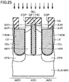
- a semiconductor substrate SUB (a cell region CER) has an active region ACR (a first region) and an inactive region IACR (a second region) defined therein alternately. Active region ACR is located between one inactive region IACR and another inactive region IACR. In active region ACR, a gate electrode GEL is disposed to extend in the y direction. Gate electrode GEL is formed in a trench TRC with a gate insulating film GIF interposed.
- An emitter electrode EEL is disposed such that it is spaced from gate electrode GEL by a distance in the x direction with active region ACR (a region of semiconductor substrate SUB) interposed and is thus disposed opposite to gate electrode GEL.
- Emitter electrode EEL extends in the y direction.
- Emitter electrode EEL is formed in trench TRC with an emitter insulating film EIF interposed.
- an n+ type source diffusion layer SDR is formed from one surface of semiconductor substrate SUB to a prescribed depth.
- a p type base diffusion layer BDR is formed from a bottom of source diffusion layer SDR to a further prescribed depth.
- Base diffusion layer BDR has a base bottom portion inclined in such a manner that a portion of the base bottom portion adjacent to emitter electrode EEL is positionally deeper than a portion of the base bottom portion adjacent to gate electrode GEL.
- a length from the portion of the base bottom portion of base diffusion layer BDR adjacent to gate electrode GEL to a lower end of gate electrode GEL is longer than a length from the portion of the base bottom portion of base diffusion layer BDR adjacent to emitter electrode EEL to the lower end of gate electrode GEL.
- An n type hole barrier layer HBR is formed from a bottom of base diffusion layer BDR to a further prescribed depth. Hole barrier layer HBR is formed to such an extent to reach the lower end portion of gate electrode GEL.
- a p type floating diffusion layer FPR is formed in inactive region IACR.
- Floating diffusion layer FPR is formed from one surface of semiconductor substrate SUB to a position deeper than a lower end portion of emitter electrode EEL.
- a contact interlayer insulating film CIL is formed to cover gate electrode GEL, source diffusion layer SDR, emitter electrode EEL, etc.
- a contact portion CCN is formed to penetrate contact interlayer insulating film CIL and thus contact emitter electrode EEL, base diffusion layer BDR, and source diffusion layer SDR.
- Contact portion CCN is formed as a common contact portion in a manner astride emitter electrode EEL and base diffusion layer BDR.
- Contact portion CCN has a contact bottom portion inclined in such a manner that a portion of the contact bottom portion in contact with emitter electrode EEL is positionally deeper than a portion of the contact bottom portion in contact with base diffusion layer BDR.
- a metal emitter electrode MEE is formed in contact with contact portion CCN.
- Metal emitter electrode MEE is formed of aluminum film for example.
- a p type collector diffusion layer CDR is formed from the other surface of semiconductor substrate SUB to a prescribed depth.
- An N type buffer layer NBR is formed from a bottom of collector diffusion layer CDR to a further prescribed depth.
- a back electrode BEL (a collector electrode) is formed in contact with collector diffusion layer CDR.
- gate electrode GEL extends to directly under a region where metal gate interconnect MGI is disposed.
- Immediately adjacent gate electrodes GELs have end portions, respectively, connected via a portion of gate electrode GEL extending in the x direction.
- a gate interconnect extracting portion MGE is formed directly under metal gate interconnect MGI. Gate interconnect extracting portion MGE is formed in contact with a portion of gate electrode GEL extending in the x direction. Gate interconnect extracting portion MGE is electrically connected to metal gate interconnect MGI via a gate contact portion GEC.
- the semiconductor device comprising the IE type trench gate IGBT has emitter electrode EEL and base and source diffusion layers BDR and SDR electrically connected by common contact portion CCN in contact with emitter electrode EEL, base diffusion layer BDR, and source diffusion layer SDR.
- Contact portion CCN has a contact bottom portion inclined in such a manner that a portion of the contact bottom portion in contact with emitter electrode EEL is positionally deeper than a portion of the contact bottom portion in contact with base diffusion layer BDR.
- base diffusion layer BDR has a base bottom portion inclined in such a manner that a portion of the base bottom portion adjacent to emitter electrode EEL is positionally deeper than a portion of the base bottom portion adjacent to gate electrode GEL.
- a length from the portion of the base bottom portion of base diffusion layer BDR adjacent to gate electrode GEL to a lower end of gate electrode GEL is longer than a length from the portion of the base bottom portion of base diffusion layer BDR adjacent to emitter electrode EEL to the lower end of gate electrode GEL.
- a PN junction of N type region NSR and collector diffusion layer CDR is forward-biased and holes are injected from collector diffusion layer CDR to N type region NSR.
- the injected holes are prevented by inactive region INCA from passing to the side of source diffusion layer SDR (or the emitter), and the holes are accumulated in N type region NSR of semiconductor substrate SUB and floating diffusion layer FPR, and an increased hole density is obtained.
- N type region NSR etc. promotes injection of electrons from source diffusion layer SDR (or the emitter), and accordingly, an increased electron density is also obtained.
- SDR source diffusion layer
- N type region NSR etc. As a carrier's density in N type region NSR etc. is thus increased, conductivity modulation arises and ON voltage can be made low.
- a silicon oxide film SOF1 is initially formed to cover one surface of a semiconductor substrate. Subsequently, with silicon oxide film SOF1 formed, a p type impurity is implanted in inactive region IACR to form a P type region PR to serve as a floating diffusion layer. Subsequently, an n type impurity is implanted in active region ACR to form an N type region NR to serve as a hole barrier layer.
- a hard mask (not shown) formed for example of silicon oxide film etc. for forming a trench is formed.
- semiconductor substrate SUB is etched to form a trench TRC (see Fig. 6 ).
- the hard mask is removed, and as shown in Fig. 6 , a surface of semiconductor substrate SUB with trench TRC formed is exposed.
- Trench TRC has a depth for example of about 3 ⁇ m to about 5 ⁇ m.
- Trench TRC has a width for example of about 0.4 ⁇ m to about 0.5 ⁇ m.
- Immediately adjacent trenches TRCs are spaced for example by about 0.8 ⁇ m to 0.9 ⁇ m. Note that these numerical values are only an example.
- a prescribed heat treatment is performed to diffuse the p type impurity of P type region PR to form floating diffusion layer FPR.
- n type impurity of N type region NR is diffused to form hole barrier layer HBR.
- a thermal oxidation process is performed to form an insulating film IF to serve as a gate insulating film etc. on a surface of semiconductor substrate SUB including an internal wall surface of trench TRC.
- a polysilicon film PSF is formed to cover semiconductor substrate SUB.
- polysilicon film PSF has a surface entirely etched to remove a portion of polysilicon film PSF located on an upper surface of semiconductor substrate SUB. Furthermore, polysilicon film PSF is over-etched. Thus, as shown in Fig. 9 , an upper surface of polysilicon film PSF remaining in trench TRC is lower in level than a surface of semiconductor substrate SUB.
- gate electrode GEL is formed in trench TRC with gate insulating film GIF interposed and emitter electrode EEL is formed in trench TRC with emitter insulating film EIF interposed.
- a silicon oxide film SOF2 is formed to cover semiconductor substrate SUB.
- a photomechanical process is performed to form a photoresist pattern (not shown) for forming a source diffusion layer and a base diffusion layer.
- a p type impurity is implanted with the photoresist pattern used as an implanting mask.
- an n type impurity is implanted with the photoresist pattern used as an implanting mask.
- the photoresist pattern is removed.
- source diffusion layer SDR is formed from a surface of semiconductor substrate SUB located in active region ACR to a prescribed depth.
- Base diffusion layer BDR is formed from a bottom of source diffusion layer SDR to a further deeper position. At this point in time, base diffusion layer BDR has a bottom portion at a substantially uniform depth.
- contact interlayer insulating film CIL is formed to cover semiconductor substrate SUB. Subsequently, a prescribed photomechanical process is performed to form a photoresist pattern (not shown) for forming a contact portion (a contact opening portion). Subsequently, by using the photoresist pattern as an etching mask, contact interlayer insulating film CIL is etched to form an opening portion HOP (see Fig. 13 ).
- etching contact interlayer insulating film CIL requires setting a condition considering an amount of etching in a subsequent etching step. Subsequently, the photoresist pattern is removed.
- contact interlayer insulating film CIL in which opening portion HOP is formed is formed as a hard mask. Opening portion HOP is formed astride source diffusion layer SDR and emitter electrode EEL. Subsequently, as shown in Fig. 14 , using contact interlayer insulating film CIL serving as the hard mask as an etching mask, source diffusion layer SDR (semiconductor substrate SUB), emitter electrode EEL (polysilicon film PSF), etc. which are exposed are etched to form a contact opening portion COP.
- emitter electrode EEL polysilicon film PSF
- source diffusion layer SDR semiconductor substrate SUB
- contact opening portion COP is deeper at a side thereof adjacent to emitter electrode EEL than at a side thereof adjacent to base diffusion layer BDR.
- emitter insulating film EIF is interposed between semiconductor substrate SUB and emitter electrode EEL (polysilicon film PSF), a portion of emitter insulating film EIF and a portion of silicon (semiconductor substrate SUB) etc. remain as a residue RES.
- contact opening portion COP has an opening bottom surface inclined in a manner in which a portion of the opening bottom surface adjacent to emitter electrode EEL is deeper than a portion of the opening bottom surface adjacent to base diffusion layer BDR.
- a p type impurity is implanted in base diffusion layer BDR by using as an implanting mask contact interlayer insulating film CIL in which contact opening portion COP is formed.
- the p type impurity is implanted from contact opening portion COP, and accordingly, in base diffusion layer BDR, a portion thereof adjacent to emitter electrode EEL is formed to a position deeper than a portion thereof adjacent to gate electrode GEL.
- Base diffusion layer BDR will thus have a base bottom portion inclined in such a manner that a portion of the base bottom portion adjacent to emitter electrode EEL is positionally deeper than a portion of the base bottom portion adjacent to gate electrode GEL.
- a barrier metal film BME such as a titanium tungsten film, is formed on contact interlayer insulating film CIL to cover an internal wall surface of contact opening portion COP.
- a barrier metal film BME such as a titanium tungsten film
- an aluminum film is formed to cover barrier metal film BME in a manner filling contact opening portion COP.
- Contact portion CCN is formed by a portion of barrier metal film BME and a portion of the aluminum film that fill contact opening portion COP.
- metal emitter electrode MEE electrically connected to contact portion CCN is formed.
- an n type impurity is implanted into the other surface of semiconductor substrate SUB to form an N type buffer layer NBR.
- a p type impurity is implanted into the other surface of semiconductor substrate SUB to form p type collector diffusion layer CDR.
- back electrode BEL in contact with collector diffusion layer CDR is formed and a major portion of the semiconductor device shown in Figs. 2 and 3 is completed.
- the semiconductor device comprising the IE type trench gate IGBT as described above can further enhance the IE effect. This will be described in comparison with a semiconductor device comprising an IE type trench gate IGBT according to a comparative example.
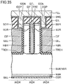
- the semiconductor device according to the comparative example is formed such that a contact portion CNE electrically connected to emitter electrode EEL and a contact portion CNP electrically connected to source diffusion layer SDR and base diffusion layer BDR are individually formed. Note that for a remainder in configuration, any member identical to that of the semiconductor device according to the first example is identically denoted and will not be described redundantly unless necessary.
- a spacing between the gate electrode and the emitter electrode (a mesa width)
- a method B increasing a distance from the base diffusion layer to a lower end of the trench (a lower end of the gate electrode)
- a method C increasing the inactive region
- enhancement of the IE effect is sought mainly from the viewpoint of method A.
- contact portion CNP when an attempt is made to narrow a mesa width MW, contact portion CNP would approach gate electrode GEL, and there is a possibility that contact portion CNP and gate electrode GEL may electrically short-circuit. Accordingly, there is a limit in narrowing mesa width MW.
- the semiconductor device according to the first example has common contact portion CCN formed as a contact portion electrically connected to emitter electrode EEL and a contact portion electrically connected to source diffusion layer SDR and base diffusion layer BDR.
- Contact portion CCN is formed astride source and base diffusion layers SDR and BDR and emitter electrode EEL.
- contact opening portion COP is formed such that emitter electrode EEL and base diffusion layer BDR are exposed at a bottom surface of contact opening portion COP and base diffusion layer BDR and source diffusion layer SDR are exposed at a side surface of contact opening portion COP.
- a p type impurity is implanted in base diffusion layer BDR from contact opening portion COP, and accordingly, in base diffusion layer BDR, a portion thereof adjacent to emitter electrode EEL will be formed to a position deeper than a portion thereof adjacent to gate electrode GEL.
- base diffusion layer BDR to have a side thereof adjacent to gate electrode GEL formed to be shallow in accordance with the inclination of the bottom portion of contact opening portion COP, and can make larger a length LG from a portion of a bottom portion of base diffusion layer BDR adjacent to gate electrode GEL to a lower end of gate electrode GEL (see Fig. 3 , method B).
- the IE effect can further be enhanced.
- a carrier i.e., holes
- N type region NSR will flow through base diffusion layer BDR at a portion adjacent to emitter electrode EEL and formed to reach a deeper position, and an operation of a parasitic transistor can be suppressed that is attributed to holes flowing through base diffusion layer BDR at a portion adjacent to gate electrode GEL.
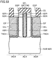
- gate electrode GEL is disposed to extend in the y direction.
- Gate electrode GEL is formed in trench TRC with gate insulating film GIF interposed.
- Emitter electrode EEL is disposed such that it is spaced from gate electrode GEL by a distance in the x direction with active region ACR (a region of semiconductor substrate SUB) interposed and is thus disposed opposite to gate electrode GEL. Emitter electrode EEL extends in the y direction. Emitter electrode EEL is formed in trench TRC with emitter insulating film EIF interposed. A width EW of emitter electrode EEL is larger than a width GW of gate electrode GEL.
- Common contact portion CCN has a contact bottom portion in contact with emitter electrode EEL. Furthermore, common contact portion CCN has a contact side portion in contact with source diffusion layer SDR and base diffusion layer BDR. An upper surface of emitter electrode EEL is lower in level than an upper surface of gate electrode GEL. Note that a remainder in configuration is similar to a configuration of the semiconductor device shown in Figs. 1-3 , and accordingly, any identical member is identically denoted and will not be described redundantly unless necessary.
- trench TRC and a trench TRCW of a prescribed depth are formed in semiconductor substrate SUB.
- a width TEW of trench TRCW in which the emitter electrode will be formed is larger than a width TGW of trench TRC in which the gate electrode will be formed.
- polysilicon film PSF is formed to cover semiconductor substrate SUB.
- polysilicon film PSF has a surface entirely etched to remove a portion of polysilicon film PSF located on an upper surface of semiconductor substrate SUB.
- polysilicon film PSF is over-etched.
- an upper surface of polysilicon film PSF remaining in trench TRC is lower in level than a surface of semiconductor substrate SUB.
- polysilicon film PSF introduced in trench TRCW having a larger width is etched at a faster rate than polysilicon film PSF introduced in trench TRC having a smaller width. Accordingly, this allows a single etching step to be done to make the position of the upper surface of polysilicon film PSF remaining in trench TRCW lower in level than the position of the upper surface of polysilicon film PSF remaining in trench TRC.
- polysilicon film PSF remaining in trench TRCW and polysilicon film PSF remaining in trench TRC may separately be etched.
- contact opening portion COP is formed to penetrate contact interlayer insulating film CIL.
- Emitter electrode EEL is exposed at a bottom surface of contact opening portion COP and source diffusion layer SDR and base diffusion layer BDR are exposed at a side surface of contact opening portion COP.
- a p type impurity is implanted in base diffusion layer BDR by using as an implanting mask contact interlayer insulating film CIL in which contact opening portion COP is formed.
- the p type impurity is implanted from contact opening portion COP, and accordingly, in base diffusion layer BDR, a portion thereof adjacent to emitter electrode EEL is formed to a position deeper than a portion thereof adjacent to gate electrode GEL.
- Base diffusion layer BDR will thus have a base bottom portion inclined in such a manner that a portion of the base bottom portion adjacent to emitter electrode EEL is positionally deeper than a portion of the base bottom portion adjacent to gate electrode GEL.
- barrier metal film BME is formed on contact interlayer insulating film CIL to cover an internal wall surface of contact opening portion COP.
- an aluminum film is formed to cover barrier metal film BME in a manner filling contact opening portion COP.
- Contact portion CCN is formed by a portion of barrier metal film BME and a portion of the aluminum film that fill contact opening portion COP.
- metal emitter electrode MEE electrically connected to contact portion CCN is formed.
- N type buffer layer NBR and p type collector diffusion layer CDR are formed at the other surface of semiconductor substrate SUB. Subsequently, back electrode BEL in contact with collector diffusion layer CDR is formed and a major portion of the semiconductor device shown in Fig. 19 and figure 20 is completed.
- emitter electrode EEL is larger in width than gate electrode GEL, and contact portion CCN has a bottom surface entirely in contact with emitter electrode EEL.
- This will be equivalent to a structure where emitter electrode EEL in the semiconductor device according to the first example is made to further approach the gate electrode GEL. This will further reduce mesa width MW between emitter electrode EEL and gate electrode GEL (method A). As a result, the IE effect can further be enhanced.
- base diffusion layer BDR can have a side thereof adjacent to gate electrode GEL formed to be shallow in accordance with the inclination of the bottom portion of contact opening portion COP, and length LG from a portion of a bottom portion of base diffusion layer BDR adjacent to gate electrode GEL to a lower end of gate electrode GEL can be made larger (see Fig. 20 , method B). This can contribute to enhancement of the IE effect.
- emitter electrode EEL larger in width than gate electrode GEL allows an increased degree of freedom in size of contact opening portion COP in which contact portion CCN is formed. This allows contact opening portion COP to have a reduced aspect ratio (depth/bottom in size), and can improve barrier metal film BME's coverage and also ensures that an aluminum film to serve as contact portion CCN is introduced.
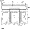
- gate electrode GEL is disposed to extend in the y direction.
- Gate electrode GEL is formed in trench TRC with gate insulating film GIF interposed.
- Emitter electrode EEL is disposed such that it is spaced from gate electrode GEL by a distance in the x direction with active region ACR (a region of semiconductor substrate SUB) interposed and is thus disposed opposite to gate electrode GEL. Emitter electrode EEL is formed throughout inactive region IACR. Emitter electrode EEL is formed in a trench TRCH with emitter insulating film EIF interposed. Emitter insulating film EIF is formed to be larger in thickness than gate insulating film GIF to ensure withstand voltage.
- Common contact portion CCN has a contact bottom portion in contact with emitter electrode EEL. Furthermore, common contact portion CCM has a contact side portion in contact with source diffusion layer SDR and base diffusion layer BDR. An upper surface of emitter electrode EEL is lower in level than an upper surface of gate electrode GEL. Note that a remainder in configuration is similar to a configuration of the semiconductor device shown in Figs. 1-3 , and accordingly, any identical member is identically denoted and will not be described redundantly unless necessary.
- trench TRC and a trench TRCH of a prescribed depth are formed in semiconductor substrate SUB.
- Trench TRCH in which an emitter electrode is to be formed is formed throughout inactive region IACR.
- a thermal oxidation process is performed to form a relatively thick insulating film IFC on a surface of semiconductor substrate SUB including an internal wall surface of trench TRC and that of trench TRCH.
- a prescribed photomechanical process is performed to form a photoresist pattern (not shown) which exposes insulating film IFC formed in trench TRC and covers insulating film IFC located in trench TRCH.
- etching is performed to remove insulating film IFC formed in trench TRC to expose semiconductor substrate SUB.
- a thermal oxidation process is performed to form a relatively thin insulating film IFN on a surface of semiconductor substrate SUB exposed in trench TRC.
- Relatively thin insulating film IFN will serve as a gate insulating film and relatively thick insulating film IFC will serve as an emitter insulating film.
- a polysilicon film (not shown) is formed in a manner filling trench TRC and trench TRCH.
- the polysilicon film has a surface entirely etched to remove a portion of the polysilicon film located on an upper surface of semiconductor substrate SUB. Furthermore, the polysilicon film is over-etched.
- an upper surface of the polysilicon film remaining in trench TRC is lower in level than a surface of semiconductor substrate SUB.
- polysilicon film PSF filling trench TRCW formed throughout inactive region IACR is etched at a faster rate than polysilicon film PSF filling trench TRC. This allows a single etching step to be done to make the position of the upper surface of polysilicon film PSF remaining in trench TRCH lower in level than the position of the upper surface of polysilicon film PSF remaining in trench TRC.
- contact opening portion COP is formed to penetrate contact interlayer insulating film CIL.
- Emitter electrode EEL is exposed at a bottom surface of contact opening portion COP and source diffusion layer SDR and base diffusion layer BDR are exposed at a side surface of contact opening portion COP.
- a p type impurity is implanted in base diffusion layer BDR by using as an implanting mask contact interlayer insulating film CIL in which contact opening portion COP is formed.
- the p type impurity is implanted from contact opening portion COP, and accordingly, in base diffusion layer BDR, a portion thereof adjacent to emitter electrode EEL is formed to a position deeper than a portion thereof adjacent to gate electrode GEL.
- Base diffusion layer BDR will thus have a base bottom portion inclined in such a manner that a portion of the base bottom portion adjacent to emitter electrode EEL is positionally deeper than a portion of the base bottom portion adjacent to gate electrode GEL.
- barrier metal film BME is formed on contact interlayer insulating film CIL to cover an internal wall surface of contact opening portion COP.
- an aluminum film is formed to cover barrier metal film BME in a manner filling contact opening portion COP.
- Contact portion CCN is formed by a portion of barrier metal film BME and a portion of the aluminum film that fill contact opening portion COP.
- metal emitter electrode MEE electrically connected to contact portion CCN is formed.
- N type buffer layer NBR and p type collector diffusion layer CDR are formed at the other surface of semiconductor substrate SUB. Subsequently, back electrode BEL in contact with collector diffusion layer CDR is formed and a major portion of the semiconductor device shown in Fig. 27 and figure 28 is completed.
- base diffusion layer BDR can have a side thereof adjacent to gate electrode GEL formed to be shallow in accordance with the inclination of the bottom portion of contact opening portion COP, and length LG from a portion of a bottom portion of base diffusion layer BDR adjacent to gate electrode GEL to a lower end of gate electrode GEL can be made larger (see Fig. 28 , method B). This can contribute to enhancement of the IE effect.
- emitter electrode EEL is formed throughout inactive region IACR. This eliminates the necessary of forming a floating diffusion layer in inactive region INACR.
- emitter insulating film EIF interposed between emitter electrode EEL and trench TRCH can be made larger in thickness than gate insulating film GIF to ensure withstand voltage at the OFF time.
- the withstand voltage can be ensured against electric field concentration at a corner of the trench.
Landscapes
- Electrodes Of Semiconductors (AREA)
Applications Claiming Priority (2)
| Application Number | Priority Date | Filing Date | Title |
|---|---|---|---|
| JP2016177746A JP6786316B2 (ja) | 2016-09-12 | 2016-09-12 | 半導体装置の製造方法 |
| EP17190374.3A EP3293770A1 (en) | 2016-09-12 | 2017-09-11 | Semiconductor device and method for producing the same |
Related Parent Applications (1)
| Application Number | Title | Priority Date | Filing Date |
|---|---|---|---|
| EP17190374.3A Division EP3293770A1 (en) | 2016-09-12 | 2017-09-11 | Semiconductor device and method for producing the same |
Publications (2)
| Publication Number | Publication Date |
|---|---|
| EP3483940A1 EP3483940A1 (en) | 2019-05-15 |
| EP3483940B1 true EP3483940B1 (en) | 2020-07-22 |
Family
ID=59856402
Family Applications (2)
| Application Number | Title | Priority Date | Filing Date |
|---|---|---|---|
| EP18211862.0A Active EP3483940B1 (en) | 2016-09-12 | 2017-09-11 | Semiconductor device and method for producing the same |
| EP17190374.3A Withdrawn EP3293770A1 (en) | 2016-09-12 | 2017-09-11 | Semiconductor device and method for producing the same |
Family Applications After (1)
| Application Number | Title | Priority Date | Filing Date |
|---|---|---|---|
| EP17190374.3A Withdrawn EP3293770A1 (en) | 2016-09-12 | 2017-09-11 | Semiconductor device and method for producing the same |
Country Status (5)
| Country | Link |
|---|---|
| US (1) | US10600896B2 (enExample) |
| EP (2) | EP3483940B1 (enExample) |
| JP (1) | JP6786316B2 (enExample) |
| CN (2) | CN107819032B (enExample) |
| TW (1) | TWI717551B (enExample) |
Families Citing this family (8)
| Publication number | Priority date | Publication date | Assignee | Title |
|---|---|---|---|---|
| JP6786316B2 (ja) * | 2016-09-12 | 2020-11-18 | ルネサスエレクトロニクス株式会社 | 半導体装置の製造方法 |
| JP7125339B2 (ja) * | 2018-12-26 | 2022-08-24 | ルネサスエレクトロニクス株式会社 | 半導体装置およびその製造方法 |
| EP3863062B1 (en) * | 2020-02-07 | 2025-05-21 | Infineon Technologies Austria AG | Semiconductor transistor device and method of manufacturing the same |
| JP7475265B2 (ja) * | 2020-12-14 | 2024-04-26 | 三菱電機株式会社 | 半導体装置及び半導体装置の製造方法 |
| KR102861154B1 (ko) | 2021-02-22 | 2025-09-17 | 삼성전자주식회사 | 반도체 장치 |
| CN113178474A (zh) * | 2021-03-02 | 2021-07-27 | 华为技术有限公司 | 半导体器件及其制作方法、及电子设备 |
| CN114496910A (zh) * | 2022-01-10 | 2022-05-13 | 上海华虹宏力半导体制造有限公司 | 双接触孔实现方法 |
| JP7731320B2 (ja) * | 2022-05-17 | 2025-08-29 | ルネサスエレクトロニクス株式会社 | 半導体装置の製造方法 |
Family Cites Families (19)
| Publication number | Priority date | Publication date | Assignee | Title |
|---|---|---|---|---|
| JP4205128B2 (ja) * | 1996-04-11 | 2009-01-07 | 三菱電機株式会社 | 高耐圧半導体装置およびその製造方法 |
| US5894149A (en) | 1996-04-11 | 1999-04-13 | Mitsubishi Denki Kabushiki Kaisha | Semiconductor device having high breakdown voltage and method of manufacturing the same |
| JP2005057028A (ja) * | 2003-08-04 | 2005-03-03 | Sanken Electric Co Ltd | 絶縁ゲート型バイポーラトランジスタ |
| JP2007207930A (ja) * | 2006-01-31 | 2007-08-16 | Toshiba Corp | 残渣処理システム、残渣処理方法及び半導体装置の製造方法 |
| KR101375035B1 (ko) * | 2006-09-27 | 2014-03-14 | 맥스파워 세미컨덕터 인크. | Mosfet 및 그 제조 방법 |
| US8264033B2 (en) * | 2009-07-21 | 2012-09-11 | Infineon Technologies Austria Ag | Semiconductor device having a floating semiconductor zone |
| US20130164895A1 (en) * | 2011-12-12 | 2013-06-27 | Maxpower Semiconductor, Inc. | Trench-Gated Power Devices with Two Types of Trenches and Reliable Polycidation |
| JP5973730B2 (ja) | 2012-01-05 | 2016-08-23 | ルネサスエレクトロニクス株式会社 | Ie型トレンチゲートigbt |
| US8946002B2 (en) * | 2012-07-24 | 2015-02-03 | Semiconductor Components Industries, Llc | Method of forming a semiconductor device having a patterned gate dielectric and structure therefor |
| JP6284314B2 (ja) * | 2012-08-21 | 2018-02-28 | ローム株式会社 | 半導体装置 |
| JP6190206B2 (ja) * | 2012-08-21 | 2017-08-30 | ローム株式会社 | 半導体装置 |
| JP5900243B2 (ja) * | 2012-08-23 | 2016-04-06 | 住友電気工業株式会社 | 炭化珪素半導体装置の製造方法 |
| JP2014075483A (ja) * | 2012-10-04 | 2014-04-24 | Sanken Electric Co Ltd | 半導体装置及び半導体装置の製造方法 |
| US9666663B2 (en) * | 2013-08-09 | 2017-05-30 | Infineon Technologies Ag | Semiconductor device with cell trench structures and contacts and method of manufacturing a semiconductor device |
| JP6354458B2 (ja) * | 2014-08-27 | 2018-07-11 | 富士電機株式会社 | 半導体装置 |
| JP5758058B1 (ja) | 2015-03-23 | 2015-08-05 | 株式会社コーチ・エィ | コーチング支援システム、コーチング支援方法、およびコーチング支援プログラム |
| JP6472714B2 (ja) * | 2015-06-03 | 2019-02-20 | ルネサスエレクトロニクス株式会社 | 半導体装置およびその製造方法 |
| JP6584893B2 (ja) * | 2015-09-25 | 2019-10-02 | ルネサスエレクトロニクス株式会社 | 半導体装置の製造方法 |
| JP6786316B2 (ja) * | 2016-09-12 | 2020-11-18 | ルネサスエレクトロニクス株式会社 | 半導体装置の製造方法 |
-
2016
- 2016-09-12 JP JP2016177746A patent/JP6786316B2/ja active Active
-
2017
- 2017-09-06 CN CN201710794982.XA patent/CN107819032B/zh active Active
- 2017-09-06 CN CN201721135203.7U patent/CN207474470U/zh not_active Withdrawn - After Issue
- 2017-09-07 TW TW106130534A patent/TWI717551B/zh active
- 2017-09-11 EP EP18211862.0A patent/EP3483940B1/en active Active
- 2017-09-11 US US15/700,337 patent/US10600896B2/en active Active
- 2017-09-11 EP EP17190374.3A patent/EP3293770A1/en not_active Withdrawn
Non-Patent Citations (1)
| Title |
|---|
| None * |
Also Published As
| Publication number | Publication date |
|---|---|
| EP3483940A1 (en) | 2019-05-15 |
| CN107819032B (zh) | 2023-10-24 |
| EP3293770A1 (en) | 2018-03-14 |
| TWI717551B (zh) | 2021-02-01 |
| JP2018046053A (ja) | 2018-03-22 |
| CN207474470U (zh) | 2018-06-08 |
| JP6786316B2 (ja) | 2020-11-18 |
| CN107819032A (zh) | 2018-03-20 |
| US10600896B2 (en) | 2020-03-24 |
| TW201826541A (zh) | 2018-07-16 |
| US20180076308A1 (en) | 2018-03-15 |
Similar Documents
| Publication | Publication Date | Title |
|---|---|---|
| EP3483940B1 (en) | Semiconductor device and method for producing the same | |
| JP7435672B2 (ja) | 半導体装置 | |
| JP7230969B2 (ja) | 半導体装置 | |
| US10777548B2 (en) | Method for manufacturing semiconductor device | |
| US6501146B1 (en) | Semiconductor device and method of manufacturing thereof | |
| JP6648838B2 (ja) | 半導体装置 | |
| US6825105B2 (en) | Manufacture of semiconductor devices with Schottky barriers | |
| JP5366297B2 (ja) | 半導体装置 | |
| CN107210322B (zh) | 半导体装置 | |
| JP7331733B2 (ja) | 半導体装置 | |
| JP7687114B2 (ja) | 半導体装置 | |
| CN109755293B (zh) | 半导体装置 | |
| JP7803330B2 (ja) | 半導体装置および半導体装置の製造方法 | |
| JP7403401B2 (ja) | 半導体装置 | |
| JP6679892B2 (ja) | 半導体装置 | |
| CN110914996A (zh) | 半导体器件 | |
| JP2023099104A (ja) | 半導体装置 | |
| CN120857529A (zh) | 半导体元件、半导体装置 | |
| JP2019087730A (ja) | 半導体装置 | |
| US20230402533A1 (en) | Semiconductor device | |
| JP6992476B2 (ja) | 半導体装置 | |
| US20240088221A1 (en) | Semiconductor device | |
| JP7677444B2 (ja) | 半導体装置の製造方法および半導体装置 | |
| KR101049446B1 (ko) | 전력 반도체 소자 | |
| CN117790583A (zh) | 碳化硅半导体装置 |
Legal Events
| Date | Code | Title | Description |
|---|---|---|---|
| PUAI | Public reference made under article 153(3) epc to a published international application that has entered the european phase |
Free format text: ORIGINAL CODE: 0009012 |
|
| STAA | Information on the status of an ep patent application or granted ep patent |
Free format text: STATUS: THE APPLICATION HAS BEEN PUBLISHED |
|
| AC | Divisional application: reference to earlier application |
Ref document number: 3293770 Country of ref document: EP Kind code of ref document: P |
|
| AK | Designated contracting states |
Kind code of ref document: A1 Designated state(s): AL AT BE BG CH CY CZ DE DK EE ES FI FR GB GR HR HU IE IS IT LI LT LU LV MC MK MT NL NO PL PT RO RS SE SI SK SM TR |
|
| AX | Request for extension of the european patent |
Extension state: BA ME |
|
| STAA | Information on the status of an ep patent application or granted ep patent |
Free format text: STATUS: REQUEST FOR EXAMINATION WAS MADE |
|
| 17P | Request for examination filed |
Effective date: 20191112 |
|
| RBV | Designated contracting states (corrected) |
Designated state(s): AL AT BE BG CH CY CZ DE DK EE ES FI FR GB GR HR HU IE IS IT LI LT LU LV MC MK MT NL NO PL PT RO RS SE SI SK SM TR |
|
| GRAP | Despatch of communication of intention to grant a patent |
Free format text: ORIGINAL CODE: EPIDOSNIGR1 |
|
| STAA | Information on the status of an ep patent application or granted ep patent |
Free format text: STATUS: GRANT OF PATENT IS INTENDED |
|
| INTG | Intention to grant announced |
Effective date: 20200204 |
|
| GRAS | Grant fee paid |
Free format text: ORIGINAL CODE: EPIDOSNIGR3 |
|
| GRAA | (expected) grant |
Free format text: ORIGINAL CODE: 0009210 |
|
| STAA | Information on the status of an ep patent application or granted ep patent |
Free format text: STATUS: THE PATENT HAS BEEN GRANTED |
|
| RIN1 | Information on inventor provided before grant (corrected) |
Inventor name: MATSUURA, HITOSHI Inventor name: MATSUO, TAKAMITSU Inventor name: SAITO, YASUYUKI Inventor name: HOSHINO, YOSHINORI |
|
| AC | Divisional application: reference to earlier application |
Ref document number: 3293770 Country of ref document: EP Kind code of ref document: P |
|
| AK | Designated contracting states |
Kind code of ref document: B1 Designated state(s): AL AT BE BG CH CY CZ DE DK EE ES FI FR GB GR HR HU IE IS IT LI LT LU LV MC MK MT NL NO PL PT RO RS SE SI SK SM TR |
|
| REG | Reference to a national code |
Ref country code: GB Ref legal event code: FG4D |
|
| REG | Reference to a national code |
Ref country code: CH Ref legal event code: EP |
|
| REG | Reference to a national code |
Ref country code: DE Ref legal event code: R096 Ref document number: 602017020362 Country of ref document: DE |
|
| REG | Reference to a national code |
Ref country code: AT Ref legal event code: REF Ref document number: 1294216 Country of ref document: AT Kind code of ref document: T Effective date: 20200815 |
|
| REG | Reference to a national code |
Ref country code: IE Ref legal event code: FG4D |
|
| REG | Reference to a national code |
Ref country code: LT Ref legal event code: MG4D |
|
| REG | Reference to a national code |
Ref country code: AT Ref legal event code: MK05 Ref document number: 1294216 Country of ref document: AT Kind code of ref document: T Effective date: 20200722 |
|
| PG25 | Lapsed in a contracting state [announced via postgrant information from national office to epo] |
Ref country code: GR Free format text: LAPSE BECAUSE OF FAILURE TO SUBMIT A TRANSLATION OF THE DESCRIPTION OR TO PAY THE FEE WITHIN THE PRESCRIBED TIME-LIMIT Effective date: 20201023 Ref country code: BG Free format text: LAPSE BECAUSE OF FAILURE TO SUBMIT A TRANSLATION OF THE DESCRIPTION OR TO PAY THE FEE WITHIN THE PRESCRIBED TIME-LIMIT Effective date: 20201022 Ref country code: NO Free format text: LAPSE BECAUSE OF FAILURE TO SUBMIT A TRANSLATION OF THE DESCRIPTION OR TO PAY THE FEE WITHIN THE PRESCRIBED TIME-LIMIT Effective date: 20201022 Ref country code: SE Free format text: LAPSE BECAUSE OF FAILURE TO SUBMIT A TRANSLATION OF THE DESCRIPTION OR TO PAY THE FEE WITHIN THE PRESCRIBED TIME-LIMIT Effective date: 20200722 Ref country code: HR Free format text: LAPSE BECAUSE OF FAILURE TO SUBMIT A TRANSLATION OF THE DESCRIPTION OR TO PAY THE FEE WITHIN THE PRESCRIBED TIME-LIMIT Effective date: 20200722 Ref country code: AT Free format text: LAPSE BECAUSE OF FAILURE TO SUBMIT A TRANSLATION OF THE DESCRIPTION OR TO PAY THE FEE WITHIN THE PRESCRIBED TIME-LIMIT Effective date: 20200722 Ref country code: LT Free format text: LAPSE BECAUSE OF FAILURE TO SUBMIT A TRANSLATION OF THE DESCRIPTION OR TO PAY THE FEE WITHIN THE PRESCRIBED TIME-LIMIT Effective date: 20200722 Ref country code: ES Free format text: LAPSE BECAUSE OF FAILURE TO SUBMIT A TRANSLATION OF THE DESCRIPTION OR TO PAY THE FEE WITHIN THE PRESCRIBED TIME-LIMIT Effective date: 20200722 Ref country code: PT Free format text: LAPSE BECAUSE OF FAILURE TO SUBMIT A TRANSLATION OF THE DESCRIPTION OR TO PAY THE FEE WITHIN THE PRESCRIBED TIME-LIMIT Effective date: 20201123 Ref country code: FI Free format text: LAPSE BECAUSE OF FAILURE TO SUBMIT A TRANSLATION OF THE DESCRIPTION OR TO PAY THE FEE WITHIN THE PRESCRIBED TIME-LIMIT Effective date: 20200722 |
|
| PG25 | Lapsed in a contracting state [announced via postgrant information from national office to epo] |
Ref country code: LV Free format text: LAPSE BECAUSE OF FAILURE TO SUBMIT A TRANSLATION OF THE DESCRIPTION OR TO PAY THE FEE WITHIN THE PRESCRIBED TIME-LIMIT Effective date: 20200722 Ref country code: RS Free format text: LAPSE BECAUSE OF FAILURE TO SUBMIT A TRANSLATION OF THE DESCRIPTION OR TO PAY THE FEE WITHIN THE PRESCRIBED TIME-LIMIT Effective date: 20200722 Ref country code: PL Free format text: LAPSE BECAUSE OF FAILURE TO SUBMIT A TRANSLATION OF THE DESCRIPTION OR TO PAY THE FEE WITHIN THE PRESCRIBED TIME-LIMIT Effective date: 20200722 Ref country code: IS Free format text: LAPSE BECAUSE OF FAILURE TO SUBMIT A TRANSLATION OF THE DESCRIPTION OR TO PAY THE FEE WITHIN THE PRESCRIBED TIME-LIMIT Effective date: 20201122 |
|
| PG25 | Lapsed in a contracting state [announced via postgrant information from national office to epo] |
Ref country code: NL Free format text: LAPSE BECAUSE OF FAILURE TO SUBMIT A TRANSLATION OF THE DESCRIPTION OR TO PAY THE FEE WITHIN THE PRESCRIBED TIME-LIMIT Effective date: 20200722 |
|
| REG | Reference to a national code |
Ref country code: DE Ref legal event code: R097 Ref document number: 602017020362 Country of ref document: DE |
|
| PG25 | Lapsed in a contracting state [announced via postgrant information from national office to epo] |
Ref country code: EE Free format text: LAPSE BECAUSE OF FAILURE TO SUBMIT A TRANSLATION OF THE DESCRIPTION OR TO PAY THE FEE WITHIN THE PRESCRIBED TIME-LIMIT Effective date: 20200722 Ref country code: RO Free format text: LAPSE BECAUSE OF FAILURE TO SUBMIT A TRANSLATION OF THE DESCRIPTION OR TO PAY THE FEE WITHIN THE PRESCRIBED TIME-LIMIT Effective date: 20200722 Ref country code: CZ Free format text: LAPSE BECAUSE OF FAILURE TO SUBMIT A TRANSLATION OF THE DESCRIPTION OR TO PAY THE FEE WITHIN THE PRESCRIBED TIME-LIMIT Effective date: 20200722 Ref country code: DK Free format text: LAPSE BECAUSE OF FAILURE TO SUBMIT A TRANSLATION OF THE DESCRIPTION OR TO PAY THE FEE WITHIN THE PRESCRIBED TIME-LIMIT Effective date: 20200722 Ref country code: IT Free format text: LAPSE BECAUSE OF FAILURE TO SUBMIT A TRANSLATION OF THE DESCRIPTION OR TO PAY THE FEE WITHIN THE PRESCRIBED TIME-LIMIT Effective date: 20200722 Ref country code: SM Free format text: LAPSE BECAUSE OF FAILURE TO SUBMIT A TRANSLATION OF THE DESCRIPTION OR TO PAY THE FEE WITHIN THE PRESCRIBED TIME-LIMIT Effective date: 20200722 |
|
| REG | Reference to a national code |
Ref country code: CH Ref legal event code: PL |
|
| PLBE | No opposition filed within time limit |
Free format text: ORIGINAL CODE: 0009261 |
|
| STAA | Information on the status of an ep patent application or granted ep patent |
Free format text: STATUS: NO OPPOSITION FILED WITHIN TIME LIMIT |
|
| PG25 | Lapsed in a contracting state [announced via postgrant information from national office to epo] |
Ref country code: AL Free format text: LAPSE BECAUSE OF FAILURE TO SUBMIT A TRANSLATION OF THE DESCRIPTION OR TO PAY THE FEE WITHIN THE PRESCRIBED TIME-LIMIT Effective date: 20200722 |
|
| REG | Reference to a national code |
Ref country code: BE Ref legal event code: MM Effective date: 20200930 |
|
| 26N | No opposition filed |
Effective date: 20210423 |
|
| PG25 | Lapsed in a contracting state [announced via postgrant information from national office to epo] |
Ref country code: SK Free format text: LAPSE BECAUSE OF FAILURE TO SUBMIT A TRANSLATION OF THE DESCRIPTION OR TO PAY THE FEE WITHIN THE PRESCRIBED TIME-LIMIT Effective date: 20200722 Ref country code: LU Free format text: LAPSE BECAUSE OF NON-PAYMENT OF DUE FEES Effective date: 20200911 |
|
| PG25 | Lapsed in a contracting state [announced via postgrant information from national office to epo] |
Ref country code: FR Free format text: LAPSE BECAUSE OF NON-PAYMENT OF DUE FEES Effective date: 20200922 |
|
| PG25 | Lapsed in a contracting state [announced via postgrant information from national office to epo] |
Ref country code: BE Free format text: LAPSE BECAUSE OF NON-PAYMENT OF DUE FEES Effective date: 20200930 Ref country code: CH Free format text: LAPSE BECAUSE OF NON-PAYMENT OF DUE FEES Effective date: 20200930 Ref country code: LI Free format text: LAPSE BECAUSE OF NON-PAYMENT OF DUE FEES Effective date: 20200930 Ref country code: SI Free format text: LAPSE BECAUSE OF FAILURE TO SUBMIT A TRANSLATION OF THE DESCRIPTION OR TO PAY THE FEE WITHIN THE PRESCRIBED TIME-LIMIT Effective date: 20200722 Ref country code: IE Free format text: LAPSE BECAUSE OF NON-PAYMENT OF DUE FEES Effective date: 20200911 |
|
| REG | Reference to a national code |
Ref country code: NL Ref legal event code: MP Effective date: 20200722 |
|
| GBPC | Gb: european patent ceased through non-payment of renewal fee |
Effective date: 20210911 |
|
| PG25 | Lapsed in a contracting state [announced via postgrant information from national office to epo] |
Ref country code: TR Free format text: LAPSE BECAUSE OF FAILURE TO SUBMIT A TRANSLATION OF THE DESCRIPTION OR TO PAY THE FEE WITHIN THE PRESCRIBED TIME-LIMIT Effective date: 20200722 Ref country code: MT Free format text: LAPSE BECAUSE OF FAILURE TO SUBMIT A TRANSLATION OF THE DESCRIPTION OR TO PAY THE FEE WITHIN THE PRESCRIBED TIME-LIMIT Effective date: 20200722 Ref country code: CY Free format text: LAPSE BECAUSE OF FAILURE TO SUBMIT A TRANSLATION OF THE DESCRIPTION OR TO PAY THE FEE WITHIN THE PRESCRIBED TIME-LIMIT Effective date: 20200722 |
|
| PG25 | Lapsed in a contracting state [announced via postgrant information from national office to epo] |
Ref country code: MK Free format text: LAPSE BECAUSE OF FAILURE TO SUBMIT A TRANSLATION OF THE DESCRIPTION OR TO PAY THE FEE WITHIN THE PRESCRIBED TIME-LIMIT Effective date: 20200722 Ref country code: MC Free format text: LAPSE BECAUSE OF FAILURE TO SUBMIT A TRANSLATION OF THE DESCRIPTION OR TO PAY THE FEE WITHIN THE PRESCRIBED TIME-LIMIT Effective date: 20200722 |
|
| PG25 | Lapsed in a contracting state [announced via postgrant information from national office to epo] |
Ref country code: GB Free format text: LAPSE BECAUSE OF NON-PAYMENT OF DUE FEES Effective date: 20210911 |
|
| REG | Reference to a national code |
Ref country code: DE Ref legal event code: R079 Ref document number: 602017020362 Country of ref document: DE Free format text: PREVIOUS MAIN CLASS: H01L0029739000 Ipc: H10D0012000000 |
|
| PGFP | Annual fee paid to national office [announced via postgrant information from national office to epo] |
Ref country code: DE Payment date: 20250926 Year of fee payment: 9 |