EP3477703B1 - Photoelectric conversion device, manufacturing method thereof, and apparatus - Google Patents
Photoelectric conversion device, manufacturing method thereof, and apparatus Download PDFInfo
- Publication number
- EP3477703B1 EP3477703B1 EP18201016.5A EP18201016A EP3477703B1 EP 3477703 B1 EP3477703 B1 EP 3477703B1 EP 18201016 A EP18201016 A EP 18201016A EP 3477703 B1 EP3477703 B1 EP 3477703B1
- Authority
- EP
- European Patent Office
- Prior art keywords
- semiconductor substrate
- silicon oxide
- oxide film
- impurity region
- boron concentration
- Prior art date
- Legal status (The legal status is an assumption and is not a legal conclusion. Google has not performed a legal analysis and makes no representation as to the accuracy of the status listed.)
- Active
Links
Images


Classifications
-
- H—ELECTRICITY
- H10—SEMICONDUCTOR DEVICES; ELECTRIC SOLID-STATE DEVICES NOT OTHERWISE PROVIDED FOR
- H10F—INORGANIC SEMICONDUCTOR DEVICES SENSITIVE TO INFRARED RADIATION, LIGHT, ELECTROMAGNETIC RADIATION OF SHORTER WAVELENGTH OR CORPUSCULAR RADIATION
- H10F77/00—Constructional details of devices covered by this subclass
- H10F77/10—Semiconductor bodies
- H10F77/12—Active materials
-
- H—ELECTRICITY
- H10—SEMICONDUCTOR DEVICES; ELECTRIC SOLID-STATE DEVICES NOT OTHERWISE PROVIDED FOR
- H10F—INORGANIC SEMICONDUCTOR DEVICES SENSITIVE TO INFRARED RADIATION, LIGHT, ELECTROMAGNETIC RADIATION OF SHORTER WAVELENGTH OR CORPUSCULAR RADIATION
- H10F39/00—Integrated devices, or assemblies of multiple devices, comprising at least one element covered by group H10F30/00, e.g. radiation detectors comprising photodiode arrays
- H10F39/011—Manufacture or treatment of image sensors covered by group H10F39/12
- H10F39/014—Manufacture or treatment of image sensors covered by group H10F39/12 of CMOS image sensors
-
- H—ELECTRICITY
- H10—SEMICONDUCTOR DEVICES; ELECTRIC SOLID-STATE DEVICES NOT OTHERWISE PROVIDED FOR
- H10F—INORGANIC SEMICONDUCTOR DEVICES SENSITIVE TO INFRARED RADIATION, LIGHT, ELECTROMAGNETIC RADIATION OF SHORTER WAVELENGTH OR CORPUSCULAR RADIATION
- H10F39/00—Integrated devices, or assemblies of multiple devices, comprising at least one element covered by group H10F30/00, e.g. radiation detectors comprising photodiode arrays
- H10F39/011—Manufacture or treatment of image sensors covered by group H10F39/12
- H10F39/028—Manufacture or treatment of image sensors covered by group H10F39/12 performed after manufacture of the image sensors, e.g. annealing, gettering of impurities, short-circuit elimination or recrystallisation
-
- H—ELECTRICITY
- H10—SEMICONDUCTOR DEVICES; ELECTRIC SOLID-STATE DEVICES NOT OTHERWISE PROVIDED FOR
- H10F—INORGANIC SEMICONDUCTOR DEVICES SENSITIVE TO INFRARED RADIATION, LIGHT, ELECTROMAGNETIC RADIATION OF SHORTER WAVELENGTH OR CORPUSCULAR RADIATION
- H10F39/00—Integrated devices, or assemblies of multiple devices, comprising at least one element covered by group H10F30/00, e.g. radiation detectors comprising photodiode arrays
- H10F39/80—Constructional details of image sensors
- H10F39/803—Pixels having integrated switching, control, storage or amplification elements
- H10F39/8033—Photosensitive area
-
- H—ELECTRICITY
- H10—SEMICONDUCTOR DEVICES; ELECTRIC SOLID-STATE DEVICES NOT OTHERWISE PROVIDED FOR
- H10F—INORGANIC SEMICONDUCTOR DEVICES SENSITIVE TO INFRARED RADIATION, LIGHT, ELECTROMAGNETIC RADIATION OF SHORTER WAVELENGTH OR CORPUSCULAR RADIATION
- H10F71/00—Manufacture or treatment of devices covered by this subclass
-
- H—ELECTRICITY
- H10—SEMICONDUCTOR DEVICES; ELECTRIC SOLID-STATE DEVICES NOT OTHERWISE PROVIDED FOR
- H10F—INORGANIC SEMICONDUCTOR DEVICES SENSITIVE TO INFRARED RADIATION, LIGHT, ELECTROMAGNETIC RADIATION OF SHORTER WAVELENGTH OR CORPUSCULAR RADIATION
- H10F77/00—Constructional details of devices covered by this subclass
- H10F77/10—Semiconductor bodies
- H10F77/14—Shape of semiconductor bodies; Shapes, relative sizes or dispositions of semiconductor regions within semiconductor bodies
-
- H—ELECTRICITY
- H10—SEMICONDUCTOR DEVICES; ELECTRIC SOLID-STATE DEVICES NOT OTHERWISE PROVIDED FOR
- H10F—INORGANIC SEMICONDUCTOR DEVICES SENSITIVE TO INFRARED RADIATION, LIGHT, ELECTROMAGNETIC RADIATION OF SHORTER WAVELENGTH OR CORPUSCULAR RADIATION
- H10F77/00—Constructional details of devices covered by this subclass
- H10F77/10—Semiconductor bodies
- H10F77/16—Material structures, e.g. crystalline structures, film structures or crystal plane orientations
-
- H—ELECTRICITY
- H10—SEMICONDUCTOR DEVICES; ELECTRIC SOLID-STATE DEVICES NOT OTHERWISE PROVIDED FOR
- H10F—INORGANIC SEMICONDUCTOR DEVICES SENSITIVE TO INFRARED RADIATION, LIGHT, ELECTROMAGNETIC RADIATION OF SHORTER WAVELENGTH OR CORPUSCULAR RADIATION
- H10F77/00—Constructional details of devices covered by this subclass
- H10F77/40—Optical elements or arrangements
- H10F77/413—Optical elements or arrangements directly associated or integrated with the devices, e.g. back reflectors
-
- H—ELECTRICITY
- H10—SEMICONDUCTOR DEVICES; ELECTRIC SOLID-STATE DEVICES NOT OTHERWISE PROVIDED FOR
- H10F—INORGANIC SEMICONDUCTOR DEVICES SENSITIVE TO INFRARED RADIATION, LIGHT, ELECTROMAGNETIC RADIATION OF SHORTER WAVELENGTH OR CORPUSCULAR RADIATION
- H10F39/00—Integrated devices, or assemblies of multiple devices, comprising at least one element covered by group H10F30/00, e.g. radiation detectors comprising photodiode arrays
- H10F39/10—Integrated devices
- H10F39/12—Image sensors
- H10F39/18—Complementary metal-oxide-semiconductor [CMOS] image sensors; Photodiode array image sensors
Definitions
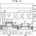
- a gate insulating film 106 is arranged on the semiconductor substrate 100.
- a gate electrode 110 is arranged on, of the semiconductor substrate 100, a region between the impurity regions 104 and 113. In other words, the gate electrode is arranged on, of the semiconductor substrate 100, a portion adjacent to the impurity region 104.
- the impurity region 104, the impurity region 113, the gate insulating film 106, and the gate electrode 110 constitute a transfer transistor.
- the n-type impurity region 104 constitutes part of the photoelectric conversion portion and has a function of accumulating charges.
- An oxide film 109 serving as hard mask is arranged on the upper surface of the gate electrode 110.
- the gate insulating film 106 and the silicon oxide film 116 contact each other, the silicon oxide film 116 and the silicon nitride film 117 contact each other, and the silicon nitride film 117 and the silicon oxide film 118 contact each other.
- the silicon nitride film 117 functions as an antireflection layer.
- the silicon oxide film 116 is arranged on the photoelectric conversion portion, and the gate insulating film 106 is arranged between the photoelectric conversion portion and the silicon oxide film 116.
- a portion on the p-type impurity region 112 may contain boron.
- the silicon oxide film 116 a portion on the p-type impurity region 112 may also contain boron. Boron contained in the gate insulating film 106 and the silicon oxide film 116 can typically be boron diffused from the impurity region 112 or may be contained in gas at the time of deposition.
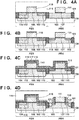
- FIG. 3A shows a position corresponding to Fig. 2 .
- a pad oxide film 105 is formed on the surface of a semiconductor substrate 100 of silicon or the like, and element isolation regions 101 are formed by STI, selective oxidation (LOCOS), or the like.
- LOCOS selective oxidation
- ion implantation is performed, forming a p-type impurity region 102 in a pixel region PXR and a p-type impurity region 103 in a peripheral circuit region PRR. These impurity regions function as well regions.
- Ion implantation is further performed, forming an n-type impurity region 104 in the impurity region 102.
- the impurity region 104 constitutes part of a photoelectric conversion portion.
- portions located above the photoelectric conversion portion are removed by plasma etching or the like, forming an opening.
- a dielectric material is buried in the opening by plasma CVD, forming a dielectric region 200.
- a wiring layer 330, an insulating member 230, and an optical member 240 are formed. In this way, the photoelectric conversion device AP in Fig. 2 is manufactured.
- the impurity region 112 is formed by ion implantation at 10 KeV or more, for example, about 13 to 15 KeV, and the silicon oxide film 116 is deposited at a deposition temperature of 620°C to 660°C.
- the abscissa of the graph in Fig. 5 indicates a position on the line X - X', and the ordinate indicates a logarithmic boron concentration at each position.
- the right direction of the abscissa is the depth direction of the semiconductor substrate 100, and the upward direction of the ordinate is the increase direction of the concentration.
- the unit is a.u. (arbitrary unit) for both the abscissa and the ordinate.
- the boron concentration at each position on the profile 502 of the second example is as follows:
Landscapes
- Solid State Image Pick-Up Elements (AREA)
- Chemical & Material Sciences (AREA)
- Light Receiving Elements (AREA)
- Crystallography & Structural Chemistry (AREA)
- Inorganic Chemistry (AREA)
- Engineering & Computer Science (AREA)
- Manufacturing & Machinery (AREA)
Applications Claiming Priority (1)
| Application Number | Priority Date | Filing Date | Title |
|---|---|---|---|
| JP2017208513A JP6978893B2 (ja) | 2017-10-27 | 2017-10-27 | 光電変換装置、その製造方法及び機器 |
Publications (2)
| Publication Number | Publication Date |
|---|---|
| EP3477703A1 EP3477703A1 (en) | 2019-05-01 |
| EP3477703B1 true EP3477703B1 (en) | 2021-03-31 |
Family
ID=63914814
Family Applications (1)
| Application Number | Title | Priority Date | Filing Date |
|---|---|---|---|
| EP18201016.5A Active EP3477703B1 (en) | 2017-10-27 | 2018-10-17 | Photoelectric conversion device, manufacturing method thereof, and apparatus |
Country Status (4)
| Country | Link |
|---|---|
| US (1) | US10686086B2 (enExample) |
| EP (1) | EP3477703B1 (enExample) |
| JP (1) | JP6978893B2 (enExample) |
| CN (1) | CN109728016B (enExample) |
Families Citing this family (2)
| Publication number | Priority date | Publication date | Assignee | Title |
|---|---|---|---|---|
| JP2020088291A (ja) * | 2018-11-29 | 2020-06-04 | キヤノン株式会社 | 光電変換装置、光電変換システム、移動体 |
| JPWO2021131539A1 (enExample) * | 2019-12-27 | 2021-07-01 |
Citations (2)
| Publication number | Priority date | Publication date | Assignee | Title |
|---|---|---|---|---|
| US20110242390A1 (en) * | 2010-03-31 | 2011-10-06 | Sony Corporation | Solid-state imaging device and electronic instrument |
| US20140346578A1 (en) * | 2013-05-23 | 2014-11-27 | Canon Kabushiki Kaisha | Solid-state image sensor, method of manufacturing the same, and image capturing system |
Family Cites Families (33)
| Publication number | Priority date | Publication date | Assignee | Title |
|---|---|---|---|---|
| US5466612A (en) * | 1992-03-11 | 1995-11-14 | Matsushita Electronics Corp. | Method of manufacturing a solid-state image pickup device |
| US6541329B1 (en) * | 2001-09-07 | 2003-04-01 | United Microelectronics Corp. | Method for making an active pixel sensor |
| JP2003218341A (ja) * | 2002-01-24 | 2003-07-31 | Sony Corp | 固体撮像素子およびその製造方法 |
| KR100450670B1 (ko) | 2002-02-09 | 2004-10-01 | 삼성전자주식회사 | 포토 다이오드를 갖는 이미지 센서 및 그 제조방법 |
| JP2004172229A (ja) * | 2002-11-18 | 2004-06-17 | Sony Corp | 固体撮像素子及びその製造方法 |
| US7215361B2 (en) * | 2003-09-17 | 2007-05-08 | Micron Technology, Inc. | Method for automated testing of the modulation transfer function in image sensors |
| US7737519B2 (en) | 2004-05-06 | 2010-06-15 | Canon Kabushiki Kaisha | Photoelectric conversion device and manufacturing method thereof |
| JP5230058B2 (ja) | 2004-06-07 | 2013-07-10 | キヤノン株式会社 | 固体撮像装置およびカメラ |
| US7605415B2 (en) | 2004-06-07 | 2009-10-20 | Canon Kabushiki Kaisha | Image pickup device comprising photoelectric conversation unit, floating diffusion region and guard ring |
| JP4424120B2 (ja) | 2004-08-31 | 2010-03-03 | ソニー株式会社 | 固体撮像装置および固体撮像装置の製造方法 |
| JP4674894B2 (ja) * | 2004-12-28 | 2011-04-20 | パナソニック株式会社 | 固体撮像装置及びその製造方法 |
| JP4718875B2 (ja) | 2005-03-31 | 2011-07-06 | 株式会社東芝 | 固体撮像素子 |
| KR100746472B1 (ko) * | 2005-09-28 | 2007-08-06 | 매그나칩 반도체 유한회사 | 시모스 이미지센서의 제조방법 |
| JP4679340B2 (ja) * | 2005-11-11 | 2011-04-27 | 株式会社東芝 | 固体撮像装置 |
| JP2007208052A (ja) | 2006-02-02 | 2007-08-16 | Fujifilm Corp | 固体撮像素子 |
| JP2008021875A (ja) | 2006-07-13 | 2008-01-31 | Toshiba Corp | 固体撮像装置 |
| JP4960058B2 (ja) | 2006-10-04 | 2012-06-27 | 株式会社東芝 | 増幅型固体撮像素子 |
| US7795655B2 (en) * | 2006-10-04 | 2010-09-14 | Sony Corporation | Solid-state imaging device and electronic device |
| JP5446281B2 (ja) * | 2008-08-01 | 2014-03-19 | ソニー株式会社 | 固体撮像装置、その製造方法および撮像装置 |
| US8338248B2 (en) * | 2008-12-25 | 2012-12-25 | National University Corporation Shizuoka University | Semiconductor element and solid-state imaging device |
| JP2010161236A (ja) * | 2009-01-08 | 2010-07-22 | Canon Inc | 光電変換装置の製造方法 |
| JP5500876B2 (ja) * | 2009-06-08 | 2014-05-21 | キヤノン株式会社 | 光電変換装置の製造方法 |
| JP5659707B2 (ja) * | 2010-11-08 | 2015-01-28 | ソニー株式会社 | 固体撮像装置とその製造方法、及び電子機器 |
| JP2012182377A (ja) * | 2011-03-02 | 2012-09-20 | Sony Corp | 固体撮像装置 |
| JP2013016675A (ja) * | 2011-07-05 | 2013-01-24 | Sony Corp | 固体撮像装置、電子機器、及び、固体撮像装置の製造方法 |
| JP5933953B2 (ja) * | 2011-10-06 | 2016-06-15 | キヤノン株式会社 | 半導体装置の製造方法 |
| JP5991739B2 (ja) * | 2012-06-15 | 2016-09-14 | キヤノン株式会社 | 固体撮像装置およびその製造方法、ならびにカメラ |
| JP6122649B2 (ja) | 2013-02-13 | 2017-04-26 | セイコーNpc株式会社 | 浅い接合を有する紫外線受光素子 |
| JP6345519B2 (ja) * | 2014-07-09 | 2018-06-20 | ルネサスエレクトロニクス株式会社 | 半導体装置の製造方法 |
| JP2016092203A (ja) * | 2014-11-04 | 2016-05-23 | 株式会社東芝 | 固体撮像装置および固体撮像装置の製造方法 |
| JP2016187018A (ja) * | 2015-03-27 | 2016-10-27 | キヤノン株式会社 | 光電変換装置およびカメラ |
| JP6821291B2 (ja) * | 2015-05-29 | 2021-01-27 | キヤノン株式会社 | 光電変換装置、撮像システムおよび光電変換装置の製造方法 |
| JP6892221B2 (ja) | 2016-03-04 | 2021-06-23 | エイブリック株式会社 | 半導体装置の製造方法 |
-
2017
- 2017-10-27 JP JP2017208513A patent/JP6978893B2/ja active Active
-
2018
- 2018-10-17 EP EP18201016.5A patent/EP3477703B1/en active Active
- 2018-10-18 US US16/163,926 patent/US10686086B2/en active Active
- 2018-10-26 CN CN201811253732.6A patent/CN109728016B/zh active Active
Patent Citations (2)
| Publication number | Priority date | Publication date | Assignee | Title |
|---|---|---|---|---|
| US20110242390A1 (en) * | 2010-03-31 | 2011-10-06 | Sony Corporation | Solid-state imaging device and electronic instrument |
| US20140346578A1 (en) * | 2013-05-23 | 2014-11-27 | Canon Kabushiki Kaisha | Solid-state image sensor, method of manufacturing the same, and image capturing system |
Also Published As
| Publication number | Publication date |
|---|---|
| US20190131468A1 (en) | 2019-05-02 |
| CN109728016B (zh) | 2023-03-17 |
| US10686086B2 (en) | 2020-06-16 |
| JP2019083230A (ja) | 2019-05-30 |
| JP6978893B2 (ja) | 2021-12-08 |
| EP3477703A1 (en) | 2019-05-01 |
| CN109728016A (zh) | 2019-05-07 |
Similar Documents
| Publication | Publication Date | Title |
|---|---|---|
| US8354631B2 (en) | Solid-state image device manufacturing method thereof, and image capturing apparatus with first and second stress liner films | |
| US6607951B2 (en) | Method for fabricating a CMOS image sensor | |
| US8525909B2 (en) | Solid-state imaging device, method for manufacturing solid-state imaging device, and imaging apparatus | |
| CN100392858C (zh) | 半导体装置、半导体装置的制造方法及其电子设备 | |
| US8518771B2 (en) | Method for manufacturing solid-state imaging device | |
| US9923023B2 (en) | Image pickup apparatus and method for manufacturing image pickup apparatus | |
| US20090121264A1 (en) | Cmos image sensor and method of forming the same | |
| JP6151499B2 (ja) | 撮像装置およびその製造方法 | |
| CN101419977B (zh) | 图像传感器及其制造方法 | |
| CN108231814A (zh) | 图像传感器及其形成方法 | |
| US10777596B2 (en) | Imaging apparatus, method of manufacturing the same, and device | |
| JP7418383B2 (ja) | 撮像装置およびカメラ | |
| EP3477703B1 (en) | Photoelectric conversion device, manufacturing method thereof, and apparatus | |
| US10916574B2 (en) | Imaging device, method of manufacturing the same, and apparatus | |
| US20150060964A1 (en) | Mechanisms for forming image sensor device | |
| CN120500126A (zh) | 一种图像传感器及其制作方法 | |
| JP2018088495A (ja) | 半導体装置および半導体装置の製造方法 | |
| US6906364B2 (en) | Structure of a CMOS image sensor | |
| US20070077678A1 (en) | Method of fabricating image sensors | |
| JP2017130693A (ja) | 撮像装置およびその製造方法 | |
| US20180006082A1 (en) | Method for manufacturing solid state image pickup apparatus | |
| JP2019161216A (ja) | 撮像装置およびその製造方法ならびに機器 |
Legal Events
| Date | Code | Title | Description |
|---|---|---|---|
| PUAI | Public reference made under article 153(3) epc to a published international application that has entered the european phase |
Free format text: ORIGINAL CODE: 0009012 |
|
| STAA | Information on the status of an ep patent application or granted ep patent |
Free format text: STATUS: THE APPLICATION HAS BEEN PUBLISHED |
|
| AK | Designated contracting states |
Kind code of ref document: A1 Designated state(s): AL AT BE BG CH CY CZ DE DK EE ES FI FR GB GR HR HU IE IS IT LI LT LU LV MC MK MT NL NO PL PT RO RS SE SI SK SM TR |
|
| AX | Request for extension of the european patent |
Extension state: BA ME |
|
| STAA | Information on the status of an ep patent application or granted ep patent |
Free format text: STATUS: REQUEST FOR EXAMINATION WAS MADE |
|
| STAA | Information on the status of an ep patent application or granted ep patent |
Free format text: STATUS: EXAMINATION IS IN PROGRESS |
|
| 17P | Request for examination filed |
Effective date: 20191104 |
|
| RBV | Designated contracting states (corrected) |
Designated state(s): AL AT BE BG CH CY CZ DE DK EE ES FI FR GB GR HR HU IE IS IT LI LT LU LV MC MK MT NL NO PL PT RO RS SE SI SK SM TR |
|
| 17Q | First examination report despatched |
Effective date: 20191217 |
|
| GRAP | Despatch of communication of intention to grant a patent |
Free format text: ORIGINAL CODE: EPIDOSNIGR1 |
|
| STAA | Information on the status of an ep patent application or granted ep patent |
Free format text: STATUS: GRANT OF PATENT IS INTENDED |
|
| INTG | Intention to grant announced |
Effective date: 20201023 |
|
| GRAS | Grant fee paid |
Free format text: ORIGINAL CODE: EPIDOSNIGR3 |
|
| GRAA | (expected) grant |
Free format text: ORIGINAL CODE: 0009210 |
|
| STAA | Information on the status of an ep patent application or granted ep patent |
Free format text: STATUS: THE PATENT HAS BEEN GRANTED |
|
| AK | Designated contracting states |
Kind code of ref document: B1 Designated state(s): AL AT BE BG CH CY CZ DE DK EE ES FI FR GB GR HR HU IE IS IT LI LT LU LV MC MK MT NL NO PL PT RO RS SE SI SK SM TR |
|
| REG | Reference to a national code |
Ref country code: GB Ref legal event code: FG4D Ref country code: CH Ref legal event code: EP |
|
| REG | Reference to a national code |
Ref country code: AT Ref legal event code: REF Ref document number: 1377914 Country of ref document: AT Kind code of ref document: T Effective date: 20210415 |
|
| REG | Reference to a national code |
Ref country code: DE Ref legal event code: R096 Ref document number: 602018014656 Country of ref document: DE |
|
| REG | Reference to a national code |
Ref country code: IE Ref legal event code: FG4D |
|
| REG | Reference to a national code |
Ref country code: LT Ref legal event code: MG9D |
|
| PG25 | Lapsed in a contracting state [announced via postgrant information from national office to epo] |
Ref country code: BG Free format text: LAPSE BECAUSE OF FAILURE TO SUBMIT A TRANSLATION OF THE DESCRIPTION OR TO PAY THE FEE WITHIN THE PRESCRIBED TIME-LIMIT Effective date: 20210630 Ref country code: HR Free format text: LAPSE BECAUSE OF FAILURE TO SUBMIT A TRANSLATION OF THE DESCRIPTION OR TO PAY THE FEE WITHIN THE PRESCRIBED TIME-LIMIT Effective date: 20210331 Ref country code: FI Free format text: LAPSE BECAUSE OF FAILURE TO SUBMIT A TRANSLATION OF THE DESCRIPTION OR TO PAY THE FEE WITHIN THE PRESCRIBED TIME-LIMIT Effective date: 20210331 Ref country code: NO Free format text: LAPSE BECAUSE OF FAILURE TO SUBMIT A TRANSLATION OF THE DESCRIPTION OR TO PAY THE FEE WITHIN THE PRESCRIBED TIME-LIMIT Effective date: 20210630 |
|
| PG25 | Lapsed in a contracting state [announced via postgrant information from national office to epo] |
Ref country code: SE Free format text: LAPSE BECAUSE OF FAILURE TO SUBMIT A TRANSLATION OF THE DESCRIPTION OR TO PAY THE FEE WITHIN THE PRESCRIBED TIME-LIMIT Effective date: 20210331 Ref country code: LV Free format text: LAPSE BECAUSE OF FAILURE TO SUBMIT A TRANSLATION OF THE DESCRIPTION OR TO PAY THE FEE WITHIN THE PRESCRIBED TIME-LIMIT Effective date: 20210331 Ref country code: RS Free format text: LAPSE BECAUSE OF FAILURE TO SUBMIT A TRANSLATION OF THE DESCRIPTION OR TO PAY THE FEE WITHIN THE PRESCRIBED TIME-LIMIT Effective date: 20210331 |
|
| REG | Reference to a national code |
Ref country code: NL Ref legal event code: MP Effective date: 20210331 |
|
| REG | Reference to a national code |
Ref country code: AT Ref legal event code: MK05 Ref document number: 1377914 Country of ref document: AT Kind code of ref document: T Effective date: 20210331 |
|
| PG25 | Lapsed in a contracting state [announced via postgrant information from national office to epo] |
Ref country code: CZ Free format text: LAPSE BECAUSE OF FAILURE TO SUBMIT A TRANSLATION OF THE DESCRIPTION OR TO PAY THE FEE WITHIN THE PRESCRIBED TIME-LIMIT Effective date: 20210331 Ref country code: EE Free format text: LAPSE BECAUSE OF FAILURE TO SUBMIT A TRANSLATION OF THE DESCRIPTION OR TO PAY THE FEE WITHIN THE PRESCRIBED TIME-LIMIT Effective date: 20210331 Ref country code: LT Free format text: LAPSE BECAUSE OF FAILURE TO SUBMIT A TRANSLATION OF THE DESCRIPTION OR TO PAY THE FEE WITHIN THE PRESCRIBED TIME-LIMIT Effective date: 20210331 Ref country code: SM Free format text: LAPSE BECAUSE OF FAILURE TO SUBMIT A TRANSLATION OF THE DESCRIPTION OR TO PAY THE FEE WITHIN THE PRESCRIBED TIME-LIMIT Effective date: 20210331 Ref country code: NL Free format text: LAPSE BECAUSE OF FAILURE TO SUBMIT A TRANSLATION OF THE DESCRIPTION OR TO PAY THE FEE WITHIN THE PRESCRIBED TIME-LIMIT Effective date: 20210331 Ref country code: AT Free format text: LAPSE BECAUSE OF FAILURE TO SUBMIT A TRANSLATION OF THE DESCRIPTION OR TO PAY THE FEE WITHIN THE PRESCRIBED TIME-LIMIT Effective date: 20210331 |
|
| PG25 | Lapsed in a contracting state [announced via postgrant information from national office to epo] |
Ref country code: IS Free format text: LAPSE BECAUSE OF FAILURE TO SUBMIT A TRANSLATION OF THE DESCRIPTION OR TO PAY THE FEE WITHIN THE PRESCRIBED TIME-LIMIT Effective date: 20210731 Ref country code: PL Free format text: LAPSE BECAUSE OF FAILURE TO SUBMIT A TRANSLATION OF THE DESCRIPTION OR TO PAY THE FEE WITHIN THE PRESCRIBED TIME-LIMIT Effective date: 20210331 Ref country code: PT Free format text: LAPSE BECAUSE OF FAILURE TO SUBMIT A TRANSLATION OF THE DESCRIPTION OR TO PAY THE FEE WITHIN THE PRESCRIBED TIME-LIMIT Effective date: 20210802 Ref country code: RO Free format text: LAPSE BECAUSE OF FAILURE TO SUBMIT A TRANSLATION OF THE DESCRIPTION OR TO PAY THE FEE WITHIN THE PRESCRIBED TIME-LIMIT Effective date: 20210331 Ref country code: SK Free format text: LAPSE BECAUSE OF FAILURE TO SUBMIT A TRANSLATION OF THE DESCRIPTION OR TO PAY THE FEE WITHIN THE PRESCRIBED TIME-LIMIT Effective date: 20210331 |
|
| REG | Reference to a national code |
Ref country code: DE Ref legal event code: R097 Ref document number: 602018014656 Country of ref document: DE |
|
| PG25 | Lapsed in a contracting state [announced via postgrant information from national office to epo] |
Ref country code: ES Free format text: LAPSE BECAUSE OF FAILURE TO SUBMIT A TRANSLATION OF THE DESCRIPTION OR TO PAY THE FEE WITHIN THE PRESCRIBED TIME-LIMIT Effective date: 20210331 Ref country code: DK Free format text: LAPSE BECAUSE OF FAILURE TO SUBMIT A TRANSLATION OF THE DESCRIPTION OR TO PAY THE FEE WITHIN THE PRESCRIBED TIME-LIMIT Effective date: 20210331 Ref country code: AL Free format text: LAPSE BECAUSE OF FAILURE TO SUBMIT A TRANSLATION OF THE DESCRIPTION OR TO PAY THE FEE WITHIN THE PRESCRIBED TIME-LIMIT Effective date: 20210331 |
|
| PLBE | No opposition filed within time limit |
Free format text: ORIGINAL CODE: 0009261 |
|
| STAA | Information on the status of an ep patent application or granted ep patent |
Free format text: STATUS: NO OPPOSITION FILED WITHIN TIME LIMIT |
|
| 26N | No opposition filed |
Effective date: 20220104 |
|
| REG | Reference to a national code |
Ref country code: CH Ref legal event code: PL |
|
| PG25 | Lapsed in a contracting state [announced via postgrant information from national office to epo] |
Ref country code: IS Free format text: LAPSE BECAUSE OF FAILURE TO SUBMIT A TRANSLATION OF THE DESCRIPTION OR TO PAY THE FEE WITHIN THE PRESCRIBED TIME-LIMIT Effective date: 20210731 |
|
| REG | Reference to a national code |
Ref country code: BE Ref legal event code: MM Effective date: 20211031 |
|
| PG25 | Lapsed in a contracting state [announced via postgrant information from national office to epo] |
Ref country code: MC Free format text: LAPSE BECAUSE OF FAILURE TO SUBMIT A TRANSLATION OF THE DESCRIPTION OR TO PAY THE FEE WITHIN THE PRESCRIBED TIME-LIMIT Effective date: 20210331 |
|
| PG25 | Lapsed in a contracting state [announced via postgrant information from national office to epo] |
Ref country code: LU Free format text: LAPSE BECAUSE OF NON-PAYMENT OF DUE FEES Effective date: 20211017 Ref country code: IT Free format text: LAPSE BECAUSE OF FAILURE TO SUBMIT A TRANSLATION OF THE DESCRIPTION OR TO PAY THE FEE WITHIN THE PRESCRIBED TIME-LIMIT Effective date: 20210331 Ref country code: BE Free format text: LAPSE BECAUSE OF NON-PAYMENT OF DUE FEES Effective date: 20211031 |
|
| PG25 | Lapsed in a contracting state [announced via postgrant information from national office to epo] |
Ref country code: LI Free format text: LAPSE BECAUSE OF NON-PAYMENT OF DUE FEES Effective date: 20211031 Ref country code: CH Free format text: LAPSE BECAUSE OF NON-PAYMENT OF DUE FEES Effective date: 20211031 |
|
| PG25 | Lapsed in a contracting state [announced via postgrant information from national office to epo] |
Ref country code: FR Free format text: LAPSE BECAUSE OF NON-PAYMENT OF DUE FEES Effective date: 20211031 |
|
| PG25 | Lapsed in a contracting state [announced via postgrant information from national office to epo] |
Ref country code: IE Free format text: LAPSE BECAUSE OF NON-PAYMENT OF DUE FEES Effective date: 20211017 |
|
| GBPC | Gb: european patent ceased through non-payment of renewal fee |
Effective date: 20221017 |
|
| PG25 | Lapsed in a contracting state [announced via postgrant information from national office to epo] |
Ref country code: CY Free format text: LAPSE BECAUSE OF FAILURE TO SUBMIT A TRANSLATION OF THE DESCRIPTION OR TO PAY THE FEE WITHIN THE PRESCRIBED TIME-LIMIT Effective date: 20210331 |
|
| PG25 | Lapsed in a contracting state [announced via postgrant information from national office to epo] |
Ref country code: HU Free format text: LAPSE BECAUSE OF FAILURE TO SUBMIT A TRANSLATION OF THE DESCRIPTION OR TO PAY THE FEE WITHIN THE PRESCRIBED TIME-LIMIT; INVALID AB INITIO Effective date: 20181017 Ref country code: GR Free format text: LAPSE BECAUSE OF FAILURE TO SUBMIT A TRANSLATION OF THE DESCRIPTION OR TO PAY THE FEE WITHIN THE PRESCRIBED TIME-LIMIT Effective date: 20210331 |
|
| PG25 | Lapsed in a contracting state [announced via postgrant information from national office to epo] |
Ref country code: GB Free format text: LAPSE BECAUSE OF NON-PAYMENT OF DUE FEES Effective date: 20221017 |
|
| PG25 | Lapsed in a contracting state [announced via postgrant information from national office to epo] |
Ref country code: MK Free format text: LAPSE BECAUSE OF FAILURE TO SUBMIT A TRANSLATION OF THE DESCRIPTION OR TO PAY THE FEE WITHIN THE PRESCRIBED TIME-LIMIT Effective date: 20210331 |
|
| PG25 | Lapsed in a contracting state [announced via postgrant information from national office to epo] |
Ref country code: TR Free format text: LAPSE BECAUSE OF FAILURE TO SUBMIT A TRANSLATION OF THE DESCRIPTION OR TO PAY THE FEE WITHIN THE PRESCRIBED TIME-LIMIT Effective date: 20210331 |
|
| PG25 | Lapsed in a contracting state [announced via postgrant information from national office to epo] |
Ref country code: MT Free format text: LAPSE BECAUSE OF FAILURE TO SUBMIT A TRANSLATION OF THE DESCRIPTION OR TO PAY THE FEE WITHIN THE PRESCRIBED TIME-LIMIT Effective date: 20210331 |
|
| REG | Reference to a national code |
Ref country code: DE Ref legal event code: R079 Ref document number: 602018014656 Country of ref document: DE Free format text: PREVIOUS MAIN CLASS: H01L0027146000 Ipc: H10F0039180000 |
|
| PGFP | Annual fee paid to national office [announced via postgrant information from national office to epo] |
Ref country code: DE Payment date: 20240919 Year of fee payment: 7 |