EP3342002B1 - Enhanced guided surface waveguide probe - Google Patents
Enhanced guided surface waveguide probe Download PDFInfo
- Publication number
- EP3342002B1 EP3342002B1 EP16757120.7A EP16757120A EP3342002B1 EP 3342002 B1 EP3342002 B1 EP 3342002B1 EP 16757120 A EP16757120 A EP 16757120A EP 3342002 B1 EP3342002 B1 EP 3342002B1
- Authority
- EP
- European Patent Office
- Prior art keywords
- conducting medium
- lossy conducting
- charge terminal
- guided surface
- coil
- Prior art date
- Legal status (The legal status is an assumption and is not a legal conclusion. Google has not performed a legal analysis and makes no representation as to the accuracy of the status listed.)
- Active
Links
Images


Classifications
-
- H—ELECTRICITY
- H03—ELECTRONIC CIRCUITRY
- H03H—IMPEDANCE NETWORKS, e.g. RESONANT CIRCUITS; RESONATORS
- H03H7/00—Multiple-port networks comprising only passive electrical elements as network components
- H03H7/18—Networks for phase shifting
- H03H7/20—Two-port phase shifters providing an adjustable phase shift
-
- H—ELECTRICITY
- H01—ELECTRIC ELEMENTS
- H01P—WAVEGUIDES; RESONATORS, LINES, OR OTHER DEVICES OF THE WAVEGUIDE TYPE
- H01P3/00—Waveguides; Transmission lines of the waveguide type
-
- H—ELECTRICITY
- H01—ELECTRIC ELEMENTS
- H01P—WAVEGUIDES; RESONATORS, LINES, OR OTHER DEVICES OF THE WAVEGUIDE TYPE
- H01P5/00—Coupling devices of the waveguide type
- H01P5/04—Coupling devices of the waveguide type with variable factor of coupling
-
- H—ELECTRICITY
- H01—ELECTRIC ELEMENTS
- H01Q—ANTENNAS, i.e. RADIO AERIALS
- H01Q1/00—Details of, or arrangements associated with, antennas
- H01Q1/04—Adaptation for subterranean or subaqueous use
-
- H—ELECTRICITY
- H01—ELECTRIC ELEMENTS
- H01Q—ANTENNAS, i.e. RADIO AERIALS
- H01Q9/00—Electrically-short antennas having dimensions not more than twice the operating wavelength and consisting of conductive active radiating elements
- H01Q9/04—Resonant antennas
-
- H—ELECTRICITY
- H01—ELECTRIC ELEMENTS
- H01Q—ANTENNAS, i.e. RADIO AERIALS
- H01Q9/00—Electrically-short antennas having dimensions not more than twice the operating wavelength and consisting of conductive active radiating elements
- H01Q9/04—Resonant antennas
- H01Q9/30—Resonant antennas with feed to end of elongated active element, e.g. unipole
- H01Q9/32—Vertical arrangement of element
-
- H—ELECTRICITY
- H02—GENERATION; CONVERSION OR DISTRIBUTION OF ELECTRIC POWER
- H02J—ELECTRIC POWER NETWORKS; CIRCUIT ARRANGEMENTS OR SYSTEMS FOR SUPPLYING OR DISTRIBUTING ELECTRIC POWER; SYSTEMS FOR STORING ELECTRIC ENERGY
- H02J50/00—Circuit arrangements or systems for wireless supply or distribution of electric power
- H02J50/20—Circuit arrangements or systems for wireless supply or distribution of electric power using microwaves or radio frequency waves
-
- H—ELECTRICITY
- H03—ELECTRONIC CIRCUITRY
- H03H—IMPEDANCE NETWORKS, e.g. RESONANT CIRCUITS; RESONATORS
- H03H7/00—Multiple-port networks comprising only passive electrical elements as network components
- H03H7/004—Capacitive coupling circuits not otherwise provided for
-
- H—ELECTRICITY
- H03—ELECTRONIC CIRCUITRY
- H03H—IMPEDANCE NETWORKS, e.g. RESONANT CIRCUITS; RESONATORS
- H03H7/00—Multiple-port networks comprising only passive electrical elements as network components
- H03H7/38—Impedance-matching networks
-
- H—ELECTRICITY
- H04—ELECTRIC COMMUNICATION TECHNIQUE
- H04B—TRANSMISSION
- H04B3/00—Line transmission systems
- H04B3/52—Systems for transmission between fixed stations via waveguides
Definitions
- radio frequency (RF) and power transmission have existed since the early 1900's.
- US-2014/252886 discloses a method comprising: positioning a charge terminal at a defined height over a lossy conducting medium, the charge terminal comprising a upper terminal portion coupled to a lower terminal portion through a variable capacitance, adjusting a phase delay of a feed network connected to the charge terminal to match a wave tilt angle corresponding to a complete Brewster angle of incidence associated with the lossy conducting medium and exciting the charge terminal with an excitation voltage via the feed network where the excitation voltage establishes an electric field that couples into a guided surface waveguide mode along a surface of the lossy conducting medium.
- Embodiments of the present disclosure are related to guided surface waveguide probes, systems and methods using guided surface waveguide modes on lossy media.
- a radiated electromagnetic field comprises electromagnetic energy that is emitted from a source structure in the form of waves that are not bound to a waveguide.
- a radiated electromagnetic field is generally a field that leaves an electric structure such as an antenna and propagates through the atmosphere or other medium and is not bound to any waveguide structure. Once radiated electromagnetic waves leave an electric structure such as an antenna, they continue to propagate in the medium of propagation (such as air) independent of their source until they dissipate regardless of whether the source continues to operate. Once electromagnetic waves are radiated, they are not recoverable unless intercepted, and, if not intercepted, the energy inherent in the radiated electromagnetic waves is lost forever.
- Radio structures such as antennas are designed to radiate electromagnetic fields by maximizing the ratio of the radiation resistance to the structure loss resistance. Radiated energy spreads out in space and is lost regardless of whether a receiver is present. The energy density of the radiated fields is a function of distance due to geometric spreading. Accordingly, the term "radiate" in all its forms as used herein refers to this form of electromagnetic propagation.
- a guided electromagnetic field is a propagating electromagnetic wave whose energy is concentrated within or near boundaries between media having different electromagnetic properties.
- a guided electromagnetic field is one that is bound to a waveguide and may be characterized as being conveyed by the current flowing in the waveguide. If there is no load to receive and/or dissipate the energy conveyed in a guided electromagnetic wave, then no energy is lost except for that dissipated in the conductivity of the guiding medium. Stated another way, if there is no load for a guided electromagnetic wave, then no energy is consumed.
- a generator or other source generating a guided electromagnetic field does not deliver real power unless a resistive load is present. To this end, such a generator or other source essentially runs idle until a load is presented.
- FIG. 1 shown is a graph 100 of field strength in decibels (dB) above an arbitrary reference in volts per meter as a function of distance in kilometers on a log-dB plot to further illustrate the distinction between radiated and guided electromagnetic fields.
- the graph 100 of FIG. 1 depicts a guided field strength curve 103 that shows the field strength of a guided electromagnetic field as a function of distance.
- This guided field strength curve 103 is essentially the same as a transmission line mode.
- the graph 100 of FIG. 1 depicts a radiated field strength curve 106 that shows the field strength of a radiated electromagnetic field as a function of distance.
- the radiated field strength curve 106 falls off geometrically (1/ d , where d is distance), which is depicted as a straight line on the log-log scale.
- the guided field strength curve 103 has a characteristic exponential decay of e ⁇ ⁇ d / d and exhibits a distinctive knee 109 on the log-log scale.
- the guided field strength curve 103 and the radiated field strength curve 106 intersect at point 112, which occurs at a crossing distance. At distances less than the crossing distance at intersection point 112, the field strength of a guided electromagnetic field is significantly greater at most locations than the field strength of a radiated electromagnetic field.
- the guided and radiated field strength curves 103 and 106 further illustrate the fundamental propagation difference between guided and radiated electromagnetic fields.
- Milligan T., Modern Antenna Design, McGraw-Hill, 1st Edition, 1985, pp.8-9 .
- the wave equation is a differential operator whose eigenfunctions possess a continuous spectrum of eigenvalues on the complex wave-number plane.
- This transverse electro-magnetic (TEM) field is called the radiation field, and those propagating fields are called "Hertzian waves.”
- TEM transverse electro-magnetic
- the wave equation plus boundary conditions mathematically lead to a spectral representation of wave-numbers composed of a continuous spectrum plus a sum of discrete spectra.
- Sommerfeld, A. "Uber die Ausbreitung der Wellen in der Drahtlosen Telegraphie," Annalen der Physik, Vol. 28, 1909, pp. 665-736 .
- ground wave and "surface wave” identify two distinctly different physical propagation phenomena.
- a surface wave arises analytically from a distinct pole yielding a discrete component in the plane wave spectrum. See, e.g., " The Excitation of Plane Surface Waves” by Cullen, A.L., (Proceedings of the IEE (British), Vol. 101, Part IV, August 1954, pp. 225-235 ).
- a surface wave is considered to be a guided surface wave.
- the surface wave in the Zenneck-Sommerfeld guided wave sense
- no t the same as the ground wave (in the Weyl-Norton-FCC sense) that is now so familiar from radio broadcasting.
- the continuous part of the wave-number eigenvalue spectrum produces the radiation field
- the discrete spectra, and corresponding residue sum arising from the poles enclosed by the contour of integration result in non-TEM traveling surface waves that are exponentially damped in the direction transverse to the propagation.
- Such surface waves are guided transmission line modes.
- Friedman, B. Principles and Techniques of Applied Mathematics, Wiley, 1956, pp. pp. 214, 283-286, 290, 298-300 .
- antennas In free space, antennas excite the continuum eigenvalues of the wave equation, which is a radiation field, where the outwardly propagating RF energy with E z and H ⁇ in-phase is lost forever.
- waveguide probes excite discrete eigenvalues, which results in transmission line propagation. See Collin, R. E., Field Theory of Guided Waves, McGraw-Hill, 1960, pp. 453, 474-477 . While such theoretical analyses have held out the hypothetical possibility of launching open surface guided waves over planar or spherical surfaces of lossy, homogeneous media, for more than a century no known structures in the engineering arts have existed for accomplishing this with any practical efficiency.
- various guided surface waveguide probes are described that are configured to excite electric fields that couple into a guided surface waveguide mode along the surface of a lossy conducting medium.
- Such guided electromagnetic fields are substantially mode-matched in magnitude and phase to a guided surface wave mode on the surface of the lossy conducting medium.
- Such a guided surface wave mode can also be termed a Zenneck waveguide mode.
- the resultant fields excited by the guided surface waveguide probes described herein are substantially mode-matched to a guided surface waveguide mode on the surface of the lossy conducting medium, a guided electromagnetic field in the form of a guided surface wave is launched along the surface of the lossy conducting medium.
- the lossy conducting medium comprises a terrestrial medium such as the Earth.
- FIG. 2 shown is a propagation interface that provides for an examination of the boundary value solutions to Maxwell's equations derived in 1907 by Jonathan Zenneck as set forth in his paper Zenneck, J., "On the Propagation of Plane Electromagnetic Waves Along a Flat Conducting Surface and their Relation to Wireless Telegraphy," Annalen der Physik, Serial 4, Vol. 23, September 20, 1907, pp. 846-866 .
- FIG. 2 depicts cylindrical coordinates for radially propagating waves along the interface between a lossy conducting medium specified as Region 1 and an insulator specified as Region 2.
- Region 1 can comprise, for example, any lossy conducting medium.
- such a lossy conducting medium can comprise a terrestrial medium such as the Earth or other medium.
- Region 2 is a second medium that shares a boundary interface with Region 1 and has different constitutive parameters relative to Region 1.
- Region 2 can comprise, for example, any insulator such as the atmosphere or other medium.
- the reflection coefficient for such a boundary interface goes to zero only for incidence at a complex Brewster angle. See Stratton, J.A., Electromagnetic Theory, McGraw-Hill, 1941, p. 516 .
- the present disclosure sets forth various guided surface waveguide probes that generate electromagnetic fields that are substantially mode-matched to a guided surface waveguide mode on the surface of the lossy conducting medium comprising Region 1.
- such electromagnetic fields substantially synthesize a wave front incident at a complex Brewster angle of the lossy conducting medium that can result in zero reflection.
- z is the vertical coordinate normal to the surface of Region 1 and ⁇ is the radial coordinate
- H n 2 ⁇ j ⁇ is a complex argument Hankel function of the second kind and order n
- u 1 is the propagation constant in the positive vertical ( z ) direction in Region 1
- u 2 is the propagation constant in the vertical ( z ) direction in Region 2
- ⁇ 1 is the conductivity of Region 1
- ⁇ is equal to 2 ⁇ f, where f is a frequency of excitation
- ⁇ o is the permittivity of free space
- ⁇ 1 is the permittivity of Region 1
- A is a source constant imposed by the source
- ⁇ is a surface wave radial propagation constant.
- x ⁇ 1 ⁇ o
- ⁇ r comprises the relative permittivity of Region 1
- ⁇ 1 is the conductivity of Region 1
- ⁇ o is the permittivity of free space
- ⁇ o comprises the permeability of free space.
- Equations (1)-(3) can be considered to be a cylindrically-symmetric, radially-propagating waveguide mode. See Barlow, H. M., and Brown, J., Radio Surface Waves, Oxford University Press, 1962, pp. 10-12, 29-33 .
- the present disclosure details structures that excite this "open boundary" waveguide mode.
- a guided surface waveguide probe is provided with a charge terminal of appropriate size that is fed with voltage and/or current and is positioned relative to the boundary interface between Region 2 and Region 1. This may be better understood with reference to FIG.
- FIG 3 which shows an example of a guided surface waveguide probe 200a that includes a charge terminal T 1 elevated above a lossy conducting medium 203 (e.g., the Earth) along a vertical axis z that is normal to a plane presented by the lossy conducting medium 203.
- the lossy conducting medium 203 makes up Region 1
- a second medium 206 makes up Region 2 and shares a boundary interface with the lossy conducting medium 203.
- the lossy conducting medium 203 can comprise a terrestrial medium such as the planet Earth.
- a terrestrial medium comprises all structures or formations included thereon whether natural or man-made.
- such a terrestrial medium can comprise natural elements such as rock, soil, sand, fresh water, sea water, trees, vegetation, and all other natural elements that make up our planet.
- such a terrestrial medium can comprise man-made elements such as concrete, asphalt, building materials, and other man-made materials.
- the lossy conducting medium 203 can comprise some medium other than the Earth, whether naturally occurring or man-made.
- the lossy conducting medium 203 can comprise other media such as man-made surfaces and structures such as automobiles, aircraft, man-made materials (such as plywood, plastic sheeting, or other materials) or other media.
- the second medium 206 can comprise the atmosphere above the ground.
- the atmosphere can be termed an "atmospheric medium” that comprises air and other elements that make up the atmosphere of the Earth.
- the second medium 206 can comprise other media relative to the lossy conducting medium 203.
- the guided surface waveguide probe 200a includes a feed network 209 that couples an excitation source 212 to the charge terminal T 1 via, e.g., a vertical feed line conductor.
- a charge Q 1 is imposed on the charge terminal T 1 to synthesize an electric field based upon the voltage applied to terminal T 1 at any given instant.
- ⁇ i the angle of incidence
- E the electric field
- Equations (1)-(6) and (17) have the nature of a transmission line mode bound to a lossy interface, not radiation fields that are associated with groundwave propagation. See Barlow, H. M. and Brown, J., Radio Surface Waves, Oxford University Press, 1962, pp. 1-5 .
- Equations (1)-(6) and (17) a review of the nature of the Hankel functions used in Equations (1)-(6) and (17) is provided for these solutions of the wave equation.
- H n 2 k ⁇ ⁇ is an outgoing wave can be recognized from its large argument asymptotic behavior that is obtained directly from the series definitions of J n ( x ) and N n ( x ).
- H n 2 x ⁇ x ⁇ ⁇ 2 ⁇ j ⁇ x j n e ⁇ jx 2 ⁇ x j n e ⁇ j x ⁇ ⁇ 4 , which, when multiplied by e j ⁇ t , is an outward propagating cylindrical wave of the form e j ( ⁇ t-k ⁇ ) with a 1 / ⁇ spatial variation.
- the Hankel function of first order and the second kind behaves as H 1 2 x ⁇ x ⁇ 0 2 ⁇ j ⁇ x . Note that these asymptotic expressions are complex quantities.
- Equations (20b) and (21) differ in phase by j , which corresponds to an extra phase advance or "phase boost" of 45° or, equivalently, ⁇ /8.
- the "far out” representation predominates over the "close-in” representation of the Hankel function.
- the distance to the Hankel crossover point (or Hankel crossover distance) can be found by equating Equations (20b) and (21) for -jyp, and solving for R x .
- x ⁇ / ⁇ o
- the far-out and close-in Hankel function asymptotes are frequency dependent, with the Hankel crossover point moving out as the frequency is lowered.
- the Hankel function asymptotes may also vary as the conductivity ( ⁇ ) of the lossy conducting medium changes. For example, the conductivity of the soil can vary with changes in weather conditions.
- the height H 1 of the elevated charge terminal T 1 in FIG. 3 affects the amount of free charge on the charge terminal T 1 .
- the charge terminal T 1 is near the ground plane of Region 1, most of the charge Q 1 on the terminal is "bound."
- the bound charge is lessened until the charge terminal T 1 reaches a height at which substantially all of the isolated charge is free.
- the advantage of an increased capacitive elevation for the charge terminal T 1 is that the charge on the elevated charge terminal T 1 is further removed from the ground plane, resulting in an increased amount of free charge q free to couple energy into the guided surface waveguide mode. As the charge terminal T 1 is moved away from the ground plane, the charge distribution becomes more uniformly distributed about the surface of the terminal. The amount of free charge is related to the self-capacitance of the charge terminal T 1 .
- the capacitance of a spherical terminal can be expressed as a function of physical height above the ground plane.
- an increase in the terminal height h reduces the capacitance C of the charge terminal.
- the charge distribution is approximately uniform about the spherical terminal, which can improve the coupling into the guided surface waveguide mode.
- the charge terminal T 1 can include any shape such as a sphere, a disk, a cylinder, a cone, a torus, a hood, one or more rings, or any other randomized shape or combination of shapes.
- An equivalent spherical diameter can be determined and used for positioning of the charge terminal T 1 .
- the charge terminal T 1 can be positioned at a physical height that is at least four times the spherical diameter (or equivalent spherical diameter) of the charge terminal T 1 to reduce the bounded charge effects.
- FIG. 5A shown is a ray optics interpretation of the electric field produced by the elevated charge Q 1 on charge terminal T 1 of FIG. 3 .
- minimizing the reflection of the incident electric field can improve and/or maximize the energy coupled into the guided surface waveguide mode of the lossy conducting medium 203.
- the ray optic interpretation shows the incident field polarized parallel to the plane of incidence having an angle of incidence of ⁇ i , which is measured with respect to the surface normal ( ⁇ ).
- This complex angle of incidence ( ⁇ i,B ) is referred to as the Brewster angle.
- Equation (22) it can be seen that the same complex Brewster angle ( ⁇ i,B ) relationship is present in both Equations (22) and (26).
- the electric field vector E can be depicted as an incoming non-uniform plane wave, polarized parallel to the plane of incidence.
- E ⁇ ⁇ i E ⁇ ⁇ ⁇ + E z z ⁇ .
- E ⁇ ⁇ z E ⁇ z cos ⁇ i
- the wave tilt angle ( ⁇ ) is equal to the angle between the normal of the wave-front at the boundary interface with Region 1 and the tangent to the boundary interface. This may be easier to see in FIG. 5B , which illustrates equi-phase surfaces of an electromagnetic wave and their normals for a radial cylindrical guided surface wave.
- the concept of an electrical effective height can provide further insight into synthesizing an electric field with a complex angle of incidence with a guided surface waveguide probe 200.
- the integration of the distributed current I ( z ) of the structure is performed over the physical height of the structure ( h p ), and normalized to the ground current ( I 0 ) flowing upward through the base (or input) of the structure.
- I C is the current that is distributed along the vertical structure of the guided surface waveguide probe 200a.
- a feed network 209 that includes a low loss coil (e.g., a helical coil) at the bottom of the structure and a vertical feed line conductor connected between the coil and the charge terminal T 1 .
- the phase delay is measured relative to the ground (stake) current I 0 .
- ray optics are used to illustrate the complex angle trigonometry of the incident electric field ( E ) having a complex Brewster angle of incidence ( ⁇ i,B ) at the Hankel crossover distance ( R x ) 121.
- a right triangle is depicted having an adjacent side of length R x along the lossy conducting medium surface and a complex Brewster angle ⁇ i,B measured between a ray 124 extending between the Hankel crossover point 121 at R x and the center of the charge terminal T 1 , and the lossy conducting medium surface 127 between the Hankel crossover point 121 and the charge terminal T 1 .
- the charge terminal T 1 positioned at physical height h p and excited with a charge having the appropriate phase delay ⁇ , the resulting electric field is incident with the lossy conducting medium boundary interface at the Hankel crossover distance R x , and at the Brewster angle. Under these conditions, the guided surface waveguide mode can be excited without reflection or substantially negligible reflection.
- FIG. 6 graphically illustrates the effect of decreasing the physical height of the charge terminal T 1 on the distance where the electric field is incident at the Brewster angle.
- the point where the electric field intersects with the lossy conducting medium (e.g., the Earth) at the Brewster angle moves closer to the charge terminal position.
- Equation (39) indicates, the height H 1 ( FIG.
- the height of the charge terminal T 1 should be at or higher than the physical height ( h p ) in order to excite the far-out component of the Hankel function.
- the height should be at least four times the spherical diameter (or equivalent spherical diameter) of the charge terminal T 1 as mentioned above.
- a guided surface waveguide probe 200 can be configured to establish an electric field having a wave tilt that corresponds to a wave illuminating the surface of the lossy conducting medium 203 at a complex Brewster angle, thereby exciting radial surface currents by substantially mode-matching to a guided surface wave mode at (or beyond) the Hankel crossover point 121 at R x .
- FIG. 7 shown is a graphical representation of an example of a guided surface waveguide probe 200b that includes a charge terminal T 1 .
- An AC source 212 acts as the excitation source for the charge terminal T 1 , which is coupled to the guided surface waveguide probe 200b through a feed network 209 ( FIG. 3 ) comprising a coil 215 such as, e.g., a helical coil.
- the AC source 212 can be inductively coupled to the coil 215 through a primary coil.
- an impedance matching network may be included to improve and/or maximize coupling of the AC source 212 to the coil 215.
- the guided surface waveguide probe 200b can include the upper charge terminal T 1 (e.g., a sphere at height h p ) that is positioned along a vertical axis z that is substantially normal to the plane presented by the lossy conducting medium 203.
- a second medium 206 is located above the lossy conducting medium 203.
- the charge terminal T 1 has a self-capacitance C T .
- charge Q 1 is imposed on the terminal T 1 depending on the voltage applied to the terminal T 1 at any given instant.
- the coil 215 is coupled to a ground stake 218 at a first end and to the charge terminal T 1 via a vertical feed line conductor 221.
- the coil connection to the charge terminal T 1 can be adjusted using a tap 224 of the coil 215 as shown in FIG. 7 .
- the coil 215 can be energized at an operating frequency by the AC source 212 through a tap 227 at a lower portion of the coil 215.
- the AC source 212 can be inductively coupled to the coil 215 through a primary coil.
- the construction and adjustment of the guided surface waveguide probe 200 is based upon various operating conditions, such as the transmission frequency, conditions of the lossy conducting medium (e.g., soil conductivity ⁇ and relative permittivity ⁇ r ), and size of the charge terminal T 1 .
- the conductivity ⁇ and relative permittivity ⁇ r can be determined through test measurements of the lossy conducting medium 203.
- the wave tilt at the Hankel crossover distance ( W Rx ) can also be found using Equation (40).
- the Hankel crossover distance can also be found by equating the magnitudes of Equations (20b) and (21) for -jyp, and solving for R x as illustrated by FIG. 4 .
- the complex effective height ( h eff ) includes a magnitude that is associated with the physical height ( h p ) of the charge terminal T 1 and a phase delay ( ⁇ ) that is to be associated with the angle ( ⁇ ) of the wave tilt at the Hankel crossover distance ( R x ).
- the feed network 209 ( FIG. 3 ) and/or the vertical feed line connecting the feed network to the charge terminal T 1 can be adjusted to match the phase ( ⁇ ) of the charge Q 1 on the charge terminal T 1 to the angle ( ⁇ ) of the wave tilt ( W ).
- the size of the charge terminal T 1 can be chosen to provide a sufficiently large surface for the charge Q 1 imposed on the terminals. In general, it is desirable to make the charge terminal T 1 as large as practical. The size of the charge terminal T 1 should be large enough to avoid ionization of the surrounding air, which can result in electrical discharge or sparking around the charge terminal.
- phase delay ⁇ c of a helically-wound coil can be determined from Maxwell's equations as has been discussed by Corum, K.L. and J.F. Corum, "RF Coils, Helical Resonators and Voltage Magnification by Coherent Spatial Modes," Microwave Review, Vol. 7, No. 2, September 2001, pp. 36-45 .
- H the axial length of the solenoidal helix
- D the coil diameter
- N the number of turns of the coil
- ⁇ ⁇ is the free-space wavelength
- the principle is the same if the helix is wound spirally or is short and fat, but V f and ⁇ c are easier to obtain by experimental measurement.
- the spatial phase delay ⁇ y of the structure can be determined using the traveling wave phase delay of the vertical feed line conductor 221 ( FIG. 7 ).
- the velocity factor is a constant with V w ⁇ 0.94, or in a range from about 0.93 to about 0.98.
- Z w 138 ⁇ log 1.123 V w ⁇ 0 2 ⁇ ⁇ a . Equation (51) implies that Z w for a single-wire feeder varies with frequency. The phase delay can be determined based upon the capacitance and characteristic impedance.
- the electric field produced by the charge oscillating Q 1 on the charge terminal T 1 is coupled into a guided surface waveguide mode traveling along the surface of a lossy conducting medium 203.
- the Brewster angle ( ⁇ i,B ) the phase delay ( ⁇ y ) associated with the vertical feed line conductor 221 ( FIG. 7 ), and the configuration of the coil 215 ( FIG.
- the position of the tap 224 may be adjusted to maximize coupling the traveling surface waves into the guided surface waveguide mode. Excess coil length beyond the position of the tap 224 can be removed to reduce the capacitive effects.
- the vertical wire height and/or the geometrical parameters of the helical coil may also be varied.
- the coupling to the guided surface waveguide mode on the surface of the lossy conducting medium 203 can be improved and/or optimized by tuning the guided surface waveguide probe 200 for standing wave resonance with respect to a complex image plane associated with the charge Q 1 on the charge terminal T 1 .
- the performance of the guided surface waveguide probe 200 can be adjusted for increased and/or maximum voltage (and thus charge Q 1 ) on the charge terminal T 1 .
- the effect of the lossy conducting medium 203 in Region 1 can be examined using image theory analysis.
- an elevated charge Q 1 placed over a perfectly conducting plane attracts the free charge on the perfectly conducting plane, which then "piles up” in the region under the elevated charge Q 1 .
- the resulting distribution of "bound” electricity on the perfectly conducting plane is similar to a bell-shaped curve.
- the boundary value problem solution that describes the fields in the region above the perfectly conducting plane may be obtained using the classical notion of image charges, where the field from the elevated charge is superimposed with the field from a corresponding "image" charge below the perfectly conducting plane.
- This analysis may also be used with respect to a lossy conducting medium 203 by assuming the presence of an effective image charge Q 1 ' beneath the guided surface waveguide probe 200.
- the effective image charge Q 1 ' coincides with the charge Q 1 on the charge terminal T 1 about a conducting image ground plane 130, as illustrated in FIG. 3 .
- the image charge Q 1 ' is not merely located at some real depth and 180° out of phase with the primary source charge Q 1 on the charge terminal T 1 , as they would be in the case of a perfect conductor. Rather, the lossy conducting medium 203 (e.g., a terrestrial medium) presents a phase shifted image.
- the image charge Q 1 ' is at a complex depth below the surface (or physical boundary) of the lossy conducting medium 203.
- complex image depth reference is made to Wait, J. R., "Complex Image Theory-Revisited,” IEEE Antennas and Propagation Magazine, Vol. 33, No. 4, August 1991, pp. 27-29 .
- the complex spacing of the image charge implies that the external field will experience extra phase shifts not encountered when the interface is either a dielectric or a perfect conductor.
- the lossy conducting medium 203 is a finitely conducting Earth 133 with a physical boundary 136.
- the finitely conducting Earth 133 may be replaced by a perfectly conducting image ground plane 139 as shown in FIG.8B , which is located at a complex depth z 1 below the physical boundary 136.
- This equivalent representation exhibits the same impedance when looking down into the interface at the physical boundary 136.
- the equivalent representation of FIG. 8B can be modeled as an equivalent transmission line, as shown in FIG. 8C .
- the depth z 1 can be determined by equating the TEM wave impedance looking down at the Earth to an image ground plane impedance z in seen looking into the transmission line of FIG. 8C .
- the guided surface waveguide probe 200b of FIG. 7 can be modeled as an equivalent single-wire transmission line image plane model that can be based upon the perfectly conducting image ground plane 139 of FIG. 8B .
- FIG. 9A shows an example of the equivalent single-wire transmission line image plane model
- FIG. 9B illustrates an example of the equivalent classic transmission line model, including the shorted transmission line of FIG. 8C .
- Z w is the characteristic impedance of the elevated vertical feed line conductor 221 in ohms
- Z c is the characteristic impedance of the coil 215 in ohms
- Z O is the characteristic impedance of free space.
- Z L 1 j ⁇ C T
- C T the self-capacitance of the charge terminal T 1
- the impedance seen "looking up” into the vertical feed line conductor 221 FIG.
- Z base Z c Z 2 + Z c tanh j ⁇ p H
- Z c + Z 2 tanh j ⁇ p H Z c Z 2 + Z c tanh j ⁇ c Z c + Z 2 tanh j ⁇ c .
- the impedance at the physical boundary 136 "looking up" into the guided surface waveguide probe 200 is the conjugate of the impedance at the physical boundary 136 "looking down" into the lossy conducting medium 203.
- the equivalent image plane models of FIGS. 9A and 9B can be tuned to resonance with respect to the image ground plane 139.
- the impedance of the equivalent complex image plane model is purely resistive, which maintains a superposed standing wave on the probe structure that maximizes the voltage and elevated charge on terminal T 1 , and by equations (1)-(3) and (16) maximizes the propagating surface wave.
- the guided surface wave excited by the guided surface waveguide probe 200 is an outward propagating traveling wave .
- the source distribution along the feed network 209 between the charge terminal T 1 and the ground stake 218 of the guided surface waveguide probe 200 ( FIGS. 3 and 7 ) is actually composed of a superposition of a traveling wave plus a standing wave on the structure.
- the phase delay of the traveling wave moving through the feed network 209 is matched to the angle of the wave tilt associated with the lossy conducting medium 203. This mode-matching allows the traveling wave to be launched along the lossy conducting medium 203.
- the load impedance Z L of the charge terminal T 1 is adjusted to bring the probe structure into standing wave resonance with respect to the image ground plane (130 of FIG. 3 or 139 of FIG. 8 ), which is at a complex depth of - d/2. In that case, the impedance seen from the image ground plane has zero reactance and the charge on the charge terminal T 1 is maximized.
- two relatively short transmission line sections of widely differing characteristic impedance may be used to provide a very large phase shift.
- a probe structure composed of two sections of transmission line, one of low impedance and one of high impedance, together totaling a physical length of, say, 0.05 ⁇ , may be fabricated to provide a phase shift of 90° which is equivalent to a 0.25 ⁇ resonance. This is due to the large jump in characteristic impedances.
- a physically short probe structure can be electrically longer than the two physical lengths combined. This is illustrated in FIGS. 9A and 9B , where the discontinuities in the impedance ratios provide large jumps in phase. The impedance discontinuity provides a substantial phase shift where the sections are joined together.
- FIG. 10 shown is a flow chart 150 illustrating an example of adjusting a guided surface waveguide probe 200 ( FIGS. 3 and 7 ) to substantially mode-match to a guided surface waveguide mode on the surface of the lossy conducting medium, which launches a guided surface traveling wave along the surface of a lossy conducting medium 203 ( FIG. 3 ).
- the charge terminal T 1 of the guided surface waveguide probe 200 is positioned at a defined height above a lossy conducting medium 203.
- the Hankel crossover distance can also be found by equating the magnitudes of Equations (20b) and (21) for -jyp, and solving for R x as illustrated by FIG. 4 .
- the complex index of refraction ( n ) can be determined using Equation (41), and the complex Brewster angle ( ⁇ i,B ) can then be determined from Equation (42).
- the physical height ( h p ) of the charge terminal T 1 can then be determined from Equation (44).
- the charge terminal T 1 should be at or higher than the physical height ( h p ) in order to excite the far-out component of the Hankel function. This height relationship is initially considered when launching surface waves.
- the height should be at least four times the spherical diameter (or equivalent spherical diameter) of the charge terminal T 1 .
- the electrical phase delay ⁇ of the elevated charge Q 1 on the charge terminal T 1 is matched to the complex wave tilt angle ⁇ .
- the phase delay ( ⁇ c ) of the helical coil and/or the phase delay ( ⁇ y ) of the vertical feed line conductor can be adjusted to make ⁇ equal to the angle ( ⁇ ) of the wave tilt (W).
- the electrical phase ⁇ can then be matched to the angle of the wave tilt. This angular (or phase) relationship is next considered when launching surface waves.
- ⁇ ⁇
- an electric field can be established at or beyond the Hankel crossover distance ( R x ) with a complex Brewster angle at the boundary interface to excite the surface waveguide mode and launch a traveling wave along the lossy conducting medium 203.
- the load impedance of the charge terminal T 1 is tuned to resonate the equivalent image plane model of the guided surface waveguide probe 200.
- the depth (d/2) of the conducting image ground plane 139 of FIG. 9A and 9B (or 130 of FIG. 3 ) can be determined using Equations (52), (53) and (54) and the values of the lossy conducting medium 203 (e.g., the Earth), which can be measured.
- the impedance ( Z in ) as seen "looking down" into the lossy conducting medium 203 can then be determined using Equation (65). This resonance relationship can be considered to maximize the launched surface waves.
- the velocity factor, phase delay, and impedance of the coil 215 and vertical feed line conductor 221 can be determined using Equations (45) through (51).
- the self-capacitance ( C T ) of the charge terminal T 1 can be determined using, e.g., Equation (24).
- the propagation factor ( ⁇ p ) of the coil 215 can be determined using Equation (35) and the propagation phase constant ( ⁇ w ) for the vertical feed line conductor 221 can be determined using Equation (49).
- the impedance ( Z base ) of the guided surface waveguide probe 200 as seen "looking up” into the coil 215 can be determined using Equations (62), (63) and (64).
- the impedance at the physical boundary 136 "looking up" into the guided surface waveguide probe 200 is the conjugate of the impedance at the physical boundary 136 "looking down" into the lossy conducting medium 203.
- An iterative approach may be taken to tune the load impedance Z L for resonance of the equivalent image plane model with respect to the conducting image ground plane 139 (or 130). In this way, the coupling of the electric field to a guided surface waveguide mode along the surface of the lossy conducting medium 203 (e.g., Earth) can be improved and/or maximized.
- the lossy conducting medium 203 e.g., Earth
- a guided surface waveguide probe 200 comprising a top-loaded vertical stub of physical height h p with a charge terminal T 1 at the top, where the charge terminal T 1 is excited through a helical coil and vertical feed line conductor at an operational frequency ( f o ) of 1.85 MHz.
- f o operational frequency
- FIG. 11 shows a plot of both over a range of frequencies. As both ⁇ and ⁇ are frequency dependent, it can be seen that their respective curves cross over each other at approximately 1.85 MHz.
- the load impedance ( Z L ) of the charge terminal T 1 can be adjusted for standing wave resonance of the equivalent image plane model of the guided surface wave probe 200.
- the coupling into the guided surface waveguide mode may be maximized.
- This can be accomplished by adjusting the capacitance of the charge terminal T 1 without changing the traveling wave phase delays of the coil and vertical feed line conductor.
- Equation (63) the impedance seen "looking up" into the vertical feed line conductor is given by Equation (63) as:
- the guided field strength curve 103 of the guided electromagnetic field has a characteristic exponential decay of e ⁇ ⁇ d / d and exhibits a distinctive knee 109 on the log-log scale.
- the surface waveguide may be considered to be "mode-matched".
- the charge terminal T 1 is of sufficient height H 1 of FIG. 3 ( h ⁇ R x tan ⁇ i , B ) so that electromagnetic waves incident onto the lossy conducting medium 203 at the complex Brewster angle do so out at a distance ( ⁇ R x ) where the 1 / r term is predominant.
- Receive circuits can be utilized with one or more guided surface waveguide probes to facilitate wireless transmission and/or power delivery systems.
- operation of a guided surface waveguide probe 200 may be controlled to adjust for variations in operational conditions associated with the guided surface waveguide probe 200.
- an adaptive probe control system 230 can be used to control the feed network 209 and/or the charge terminal T 1 to control the operation of the guided surface waveguide probe 200.
- Operational conditions can include, but are not limited to, variations in the characteristics of the lossy conducting medium 203 (e.g., conductivity ⁇ and relative permittivity ⁇ r ), variations in field strength and/or variations in loading of the guided surface waveguide probe 200.
- e j ⁇ ) can be affected by changes in soil conductivity and permittivity resulting from, e.g ., weather conditions.
- Equipment such as, e.g., conductivity measurement probes, permittivity sensors, ground parameter meters, field meters, current monitors and/or load receivers can be used to monitor for changes in the operational conditions and provide information about current operational conditions to the adaptive probe control system 230.
- the probe control system 230 can then make one or more adjustments to the guided surface waveguide probe 200 to maintain specified operational conditions for the guided surface waveguide probe 200. For instance, as the moisture and temperature vary, the conductivity of the soil will also vary.
- Conductivity measurement probes and/or permittivity sensors may be located at multiple locations around the guided surface waveguide probe 200. Generally, it would be desirable to monitor the conductivity and/or permittivity at or about the Hankel crossover distance R x for the operational frequency.
- Conductivity measurement probes and/or permittivity sensors may be located at multiple locations ( e.g., in each quadrant) around the guided surface waveguide probe 200.
- the conductivity measurement probes and/or permittivity sensors can be configured to evaluate the conductivity and/or permittivity on a periodic basis and communicate the information to the probe control system 230.
- the information may be communicated to the probe control system 230 through a network such as, but not limited to, a LAN, WLAN, cellular network, or other appropriate wired or wireless communication network.
- the probe control system 230 may evaluate the variation in the index of refraction ( n ), the complex Brewster angle ( ⁇ i,B ), and/or the wave tilt (
- the probe control system 230 can adjust the self-capacitance of the charge terminal T 1 and/or the phase delay ( ⁇ y , ⁇ c ) applied to the charge terminal T 1 to maintain the electrical launching efficiency of the guided surface wave at or near its maximum.
- the self-capacitance of the charge terminal T 1 can be varied by changing the size of the terminal.
- the charge distribution can also be improved by increasing the size of the charge terminal T 1 , which can reduce the chance of an electrical discharge from the charge terminal T 1 .
- the charge terminal T 1 can include a variable inductance that can be adjusted to change the load impedance Z L .
- the phase applied to the charge terminal T 1 can be adjusted by varying the tap position on the coil 215 ( FIG. 7 ), and/or by including a plurality of predefined taps along the coil 215 and switching between the different predefined tap locations to maximize the launching efficiency.
- Field or field strength (FS) meters may also be distributed about the guided surface waveguide probe 200 to measure field strength of fields associated with the guided surface wave.
- the field or FS meters can be configured to detect the field strength and/or changes in the field strength (e.g., electric field strength) and communicate that information to the probe control system 230.
- the information may be communicated to the probe control system 230 through a network such as, but not limited to, a LAN, WLAN, cellular network, or other appropriate communication network.
- the guided surface waveguide probe 200 may be adjusted to maintain specified field strength(s) at the FS meter locations to ensure appropriate power transmission to the receivers and the loads they supply.
- the guided surface waveguide probe 200 can be adjusted to ensure the wave tilt corresponds to the complex Brewster angle. This can be accomplished by adjusting a tap position on the coil 215 ( FIG. 7 ) to change the phase delay supplied to the charge terminal T 1 .
- the voltage level supplied to the charge terminal T 1 can also be increased or decreased to adjust the electric field strength. This may be accomplished by adjusting the output voltage of the excitation source 212 or by adjusting or reconfiguring the feed network 209. For instance, the position of the tap 227 ( FIG.
- the AC source 212 can be adjusted to increase the voltage seen by the charge terminal T 1 . Maintaining field strength levels within predefined ranges can improve coupling by the receivers, reduce ground current losses, and avoid interference with transmissions from other guided surface waveguide probes 200.
- the probe control system 230 can be implemented with hardware, firmware, software executed by hardware, or a combination thereof.
- the probe control system 230 can include processing circuitry including a processor and a memory, both of which can be coupled to a local interface such as, for example, a data bus with an accompanying control/address bus as can be appreciated by those with ordinary skill in the art.
- a probe control application may be executed by the processor to adjust the operation of the guided surface waveguide probe 200 based upon monitored conditions.
- the probe control system 230 can also include one or more network interfaces for communicating with the various monitoring devices. Communications can be through a network such as, but not limited to, a LAN, WLAN, cellular network, or other appropriate communication network.
- the probe control system 230 may comprise, for example, a computer system such as a server, desktop computer, laptop, or other system with like capability.
- the complex angle trigonometry is shown for the ray optic interpretation of the incident electric field ( E ) of the charge terminal T 1 with a complex Brewster angle ( ⁇ i,B ) at the Hankel crossover distance ( R x ).
- the Brewster angle is complex and specified by equation (38).
- the geometric parameters are related by the electrical effective height ( h eff ) of the charge terminal T 1 by equation (39).
- the angle of the desired guided surface wave tilt at the Hankel crossover distance ( W Rx ) is equal to the phase ( ⁇ ) of the complex effective height ( h eff ).
- the charge terminal T 1 positioned at the physical height h p and excited with a charge having the appropriate phase ⁇ , the resulting electric field is incident with the lossy conducting medium boundary interface at the Hankel crossover distance R x , and at the Brewster angle. Under these conditions, the guided surface waveguide mode can be excited without reflection or substantially negligible reflection.
- Equation (39) means that the physical height of the guided surface waveguide probe 200 can be relatively small. While this will excite the guided surface waveguide mode, this can result in an unduly large bound charge with little free charge.
- the charge terminal T 1 can be raised to an appropriate elevation to increase the amount of free charge. As one example rule of thumb, the charge terminal T 1 can be positioned at an elevation of about 4-5 times (or more) the effective diameter of the charge terminal T 1 .
- FIG. 6 illustrates the effect of raising the charge terminal T 1 above the physical height ( h p ) shown in FIG. 5A . The increased elevation causes the distance at which the wave tilt is incident with the lossy conductive medium to move beyond the Hankel crossover point 121 ( FIG. 5A ).
- a lower compensation terminal T 2 can be used to adjust the total effective height ( h TE ) of the charge terminal T 1 such that the wave tilt at the Hankel crossover distance is at the Brewster angle.
- a guided surface waveguide probe 200c that includes an elevated charge terminal T 1 and a lower compensation terminal T 2 that are arranged along a vertical axis z that is normal to a plane presented by the lossy conducting medium 203.
- the charge terminal T 1 is placed directly above the compensation terminal T 2 although it is possible that some other arrangement of two or more charge and/or compensation terminals T N can be used.
- the guided surface waveguide probe 200c is disposed above a lossy conducting medium 203 according to an embodiment of the present disclosure.
- the lossy conducting medium 203 makes up Region 1 with a second medium 206 that makes up Region 2 sharing a boundary interface with the lossy conducting medium 203.
- the guided surface waveguide probe 200c includes a feed network 209 that couples an excitation source 212 to the charge terminal T 1 and the compensation terminal T 2 .
- charges Q 1 and Q 2 can be imposed on the respective charge and compensation terminals T 1 and T 2 , depending on the voltages applied to terminals T 1 and T 2 at any given instant.
- I 1 is the conduction current feeding the charge Q 1 on the charge terminal T 1 via the terminal lead
- I 2 is the conduction current feeding the charge Q 2 on the compensation terminal T 2 via the terminal lead.
- the charge terminal T 1 is positioned over the lossy conducting medium 203 at a physical height H 1
- the compensation terminal T 2 is positioned directly below T 1 along the vertical axis z at a physical height H 2 , where H 2 is less than H 1 .
- the charge terminal T 1 has an isolated (or self) capacitance C 1
- the compensation terminal T 2 has an isolated (or self) capacitance C 2 .
- a mutual capacitance C M can also exist between the terminals T 1 and T 2 depending on the distance therebetween.
- charges Q 1 and Q 2 are imposed on the charge terminal T 1 and the compensation terminal T 2 , respectively, depending on the voltages applied to the charge terminal T 1 and the compensation terminal T 2 at any given instant.
- FIG. 13 shown is a ray optics interpretation of the effects produced by the elevated charge Q 1 on charge terminal T 1 and compensation terminal T 2 of FIG. 12 .
- the compensation terminal T 2 can be used to adjust h TE by compensating for the increased height.
- the effect of the compensation terminal T 2 is to reduce the electrical effective height of the guided surface waveguide probe (or effectively raise the lossy medium interface) such that the wave tilt at the Hankel crossover distance is at the Brewster angle as illustrated by line 166.
- the lower effective height can be used to adjust the total effective height ( h TE ) to equal the complex effective height ( h eff ) of FIG. 5A .
- Equations (85) or (86) can be used to determine the physical height of the lower disk of the compensation terminal T 2 and the phase angles to feed the terminals in order to obtain the desired wave tilt at the Hankel crossover distance.
- the total effective height ( h TE ) is the superposition of the complex effective height ( h UE ) of the upper charge terminal T 1 and the complex effective height ( h LE ) of the lower compensation terminal T 2 as expressed in Equation (86).
- the h TE can be adjusted to make the wave tilt of the incident ray match the complex Brewster angle at the Hankel crossover point 121. This can be accomplished by adjusting h p , ⁇ U , and/or h d .
- FIG. 14 shown is a graphical representation of an example of a guided surface waveguide probe 200d including an upper charge terminal T 1 (e.g., a sphere at height h T ) and a lower compensation terminal T 2 ( e.g., a disk at height h d ) that are positioned along a vertical axis z that is substantially normal to the plane presented by the lossy conducting medium 203.
- charges Q 1 and Q 2 are imposed on the charge and compensation terminals T 1 and T 2 , respectively, depending on the voltages applied to the terminals T 1 and T 2 at any given instant.
- An AC source 212 acts as the excitation source for the charge terminal T 1 , which is coupled to the guided surface waveguide probe 200d through a feed network 209 comprising a coil 215 such as, e.g., a helical coil.
- the AC source 212 can be connected across a lower portion of the coil 215 through a tap 227, as shown in FIG. 14 , or can be inductively coupled to the coil 215 by way of a primary coil.
- the coil 215 can be coupled to a ground stake 218 at a first end and the charge terminal T 1 at a second end. In some implementations, the connection to the charge terminal T 1 can be adjusted using a tap 224 at the second end of the coil 215.
- the compensation terminal T 2 is positioned above and substantially parallel with the lossy conducting medium 203 (e.g., the ground or Earth), and energized through a tap 233 coupled to the coil 215.
- An ammeter 236 located between the coil 215 and ground stake 218 can be used to provide an indication of the magnitude of the current flow ( I 0 ) at the base of the guided surface waveguide probe.
- a current clamp may be used around the conductor coupled to the ground stake 218 to obtain an indication of the magnitude of the current flow ( I 0 ).
- the coil 215 is coupled to a ground stake 218 at a first end and the charge terminal T 1 at a second end via a vertical feed line conductor 221.
- the connection to the charge terminal T 1 can be adjusted using a tap 224 at the second end of the coil 215 as shown in FIG. 14 .
- the coil 215 can be energized at an operating frequency by the AC source 212 through a tap 227 at a lower portion of the coil 215.
- the AC source 212 can be inductively coupled to the coil 215 through a primary coil.
- the compensation terminal T 2 is energized through a tap 233 coupled to the coil 215.
- An ammeter 236 located between the coil 215 and ground stake 218 can be used to provide an indication of the magnitude of the current flow at the base of the guided surface waveguide probe 200d.
- a current clamp may be used around the conductor coupled to the ground stake 218 to obtain an indication of the magnitude of the current flow.
- the compensation terminal T 2 is positioned above and substantially parallel with the lossy conducting medium 203 ( e.g., the ground).
- connection to the charge terminal T 1 located on the coil 215 above the connection point of tap 233 for the compensation terminal T 2 allows an increased voltage (and thus a higher charge Q 1 ) to be applied to the upper charge terminal T 1 .
- the connection points for the charge terminal T 1 and the compensation terminal T 2 can be reversed. It is possible to adjust the total effective height ( h TE ) of the guided surface waveguide probe 200d to excite an electric field having a guided surface wave tilt at the Hankel crossover distance R x .
- the Hankel crossover distance can also be found by equating the magnitudes of equations (20b) and (21) for -jyp, and solving for R x as illustrated by FIG. 4 .
- e j ⁇ ) and the complex effective height ( h eff h p e j ⁇ ) can be determined as described with respect to Equations (41) - (44) above.
- a spherical diameter (or the effective spherical diameter) can be determined.
- the terminal configuration may be modeled as a spherical capacitance having an effective spherical diameter.
- the size of the charge terminal T 1 can be chosen to provide a sufficiently large surface for the charge Q 1 imposed on the terminals. In general, it is desirable to make the charge terminal T 1 as large as practical. The size of the charge terminal T 1 should be large enough to avoid ionization of the surrounding air, which can result in electrical discharge or sparking around the charge terminal.
- the desired elevation to provide free charge on the charge terminal T 1 for launching a guided surface wave should be at least 4-5 times the effective spherical diameter above the lossy conductive medium ( e.g., the Earth).
- the compensation terminal T 2 can be used to adjust the total effective height ( h TE ) of the guided surface waveguide probe 200d to excite an electric field having a guided surface wave tilt at R x .
- the coil phase ⁇ U can be determined from Re ⁇ U ⁇ , as graphically illustrated in plot 175.
- FIG. 15B shows a schematic diagram of the general electrical hookup of FIG. 14 in which V 1 is the voltage applied to the lower portion of the coil 215 from the AC source 212 through tap 227, V 2 is the voltage at tap 224 that is supplied to the upper charge terminal T 1 , and V 3 is the voltage applied to the lower compensation terminal T 2 through tap 233.
- the resistances R p and R d represent the ground return resistances of the charge terminal T 1 and compensation terminal T 2 , respectively.
- the charge and compensation terminals T 1 and T 2 may be configured as spheres, cylinders, toroids, rings, hoods, or any other combination of capacitive structures.
- the size of the charge and compensation terminals T 1 and T 2 can be chosen to provide a sufficiently large surface for the charges Q 1 and Q 2 imposed on the terminals. In general, it is desirable to make the charge terminal T 1 as large as practical.
- the size of the charge terminal T 1 should be large enough to avoid ionization of the surrounding air, which can result in electrical discharge or sparking around the charge terminal.
- the self-capacitance C p and C d of the charge and compensation terminals T 1 and T 2 respectively, can be determined using, for example, equation (24).
- a resonant circuit is formed by at least a portion of the inductance of the coil 215, the self-capacitance C d of the compensation terminal T 2 , and the ground return resistance R d associated with the compensation terminal T 2 .
- the parallel resonance can be established by adjusting the voltage V 3 applied to the compensation terminal T 2 ( e.g., by adjusting a tap 233 position on the coil 215) or by adjusting the height and/or size of the compensation terminal T 2 to adjust C d .
- the position of the coil tap 233 can be adjusted for parallel resonance, which will result in the ground current through the ground stake 218 and through the ammeter 236 reaching a maximum point.
- the position of the tap 227 for the AC source 212 can be adjusted to the 50 ⁇ point on the coil 215.
- Voltage V 2 from the coil 215 can be applied to the charge terminal T 1 , and the position of tap 224 can be adjusted such that the phase ( ⁇ ) of the total effective height ( h TE ) approximately equals the angle of the guided surface wave tilt ( W Rx ) at the Hankel crossover distance ( R x ).
- the position of the coil tap 224 can be adjusted until this operating point is reached, which results in the ground current through the ammeter 236 increasing to a maximum.
- the resultant fields excited by the guided surface waveguide probe 200d are substantially mode-matched to a guided surface waveguide mode on the surface of the lossy conducting medium 203, resulting in the launching of a guided surface wave along the surface of the lossy conducting medium 203. This can be verified by measuring field strength along a radial extending from the guided surface waveguide probe 200.
- Resonance of the circuit including the compensation terminal T 2 may change with the attachment of the charge terminal T 1 and/or with adjustment of the voltage applied to the charge terminal T 1 through tap 224. While adjusting the compensation terminal circuit for resonance aids the subsequent adjustment of the charge terminal connection, it is not necessary to establish the guided surface wave tilt ( W Rx ) at the Hankel crossover distance ( R x ).
- the system may be further adjusted to improve coupling by iteratively adjusting the position of the tap 227 for the AC source 212 to be at the 50 ⁇ point on the coil 215 and adjusting the position of tap 233 to maximize the ground current through the ammeter 236. Resonance of the circuit including the compensation terminal T 2 may drift as the positions of taps 227 and 233 are adjusted, or when other components are attached to the coil 215.
- the voltage V 2 from the coil 215 can be applied to the charge terminal T 1 , and the position of tap 233 can be adjusted such that the phase ( ⁇ ) of the total effective height ( h TE ) approximately equals the angle ( ⁇ ) of the guided surface wave tilt at R x .
- the position of the coil tap 224 can be adjusted until the operating point is reached, resulting in the ground current through the ammeter 236 substantially reaching a maximum.
- the resultant fields are substantially mode-matched to a guided surface waveguide mode on the surface of the lossy conducting medium 203, and a guided surface wave is launched along the surface of the lossy conducting medium 203. This can be verified by measuring field strength along a radial extending from the guided surface waveguide probe 200.
- the system may be further adjusted to improve coupling by iteratively adjusting the position of the tap 227 for the AC source 212 to be at the 50 ⁇ point on the coil 215 and adjusting the position of tap 224 and/or 233 to maximize the ground current through the ammeter 236.
- operation of a guided surface waveguide probe 200 may be controlled to adjust for variations in operational conditions associated with the guided surface waveguide probe 200.
- a probe control system 230 can be used to control the feed network 209 and/or positioning of the charge terminal T 1 and/or compensation terminal T 2 to control the operation of the guided surface waveguide probe 200.
- Operational conditions can include, but are not limited to, variations in the characteristics of the lossy conducting medium 203 (e.g., conductivity ⁇ and relative permittivity ⁇ r ), variations in field strength and/or variations in loading of the guided surface waveguide probe 200.
- e j ⁇ ) and the complex effective height ( h eff h p e j ⁇ ) can be affected by changes in soil conductivity and permittivity resulting from, e.g ., weather conditions.
- Equipment such as, e.g., conductivity measurement probes, permittivity sensors, ground parameter meters, field meters, current monitors and/or load receivers can be used to monitor for changes in the operational conditions and provide information about current operational conditions to the probe control system 230.
- the probe control system 230 can then make one or more adjustments to the guided surface waveguide probe 200 to maintain specified operational conditions for the guided surface waveguide probe 200. For instance, as the moisture and temperature vary, the conductivity of the soil will also vary.
- Conductivity measurement probes and/or permittivity sensors may be located at multiple locations around the guided surface waveguide probe 200. Generally, it would be desirable to monitor the conductivity and/or permittivity at or about the Hankel crossover distance R x for the operational frequency.
- Conductivity measurement probes and/or permittivity sensors may be located at multiple locations ( e.g., in each quadrant) around the guided surface waveguide probe 200.
- a guided surface waveguide probe 200e that includes a charge terminal T 1 and a charge terminal T 2 that are arranged along a vertical axis z.
- the guided surface waveguide probe 200e is disposed above a lossy conducting medium 203, which makes up Region 1.
- a second medium 206 shares a boundary interface with the lossy conducting medium 203 and makes up Region 2.
- the charge terminals T 1 and T 2 are positioned over the lossy conducting medium 203.
- the charge terminal T 1 is positioned at height H 1
- the charge terminal T 2 is positioned directly below T 1 along the vertical axis z at height H 2 , where H 2 is less than H 1 .
- the guided surface waveguide probe 200e includes a feed network 209 that couples an excitation source 212 to the charge terminals T 1 and T 2 .
- the charge terminals T 1 and/or T 2 include a conductive mass that can hold an electrical charge, which may be sized to hold as much charge as practically possible.
- the charge terminal T 1 has a self-capacitance C 1
- the charge terminal T 2 has a self-capacitance C 2 , which can be determined using, for example, equation (24).
- a mutual capacitance C M is created between the charge terminals T 1 and T 2 .
- the charge terminals T 1 and T 2 need not be identical, but each can have a separate size and shape, and can include different conducting materials.
- the field strength of a guided surface wave launched by a guided surface waveguide probe 200e is directly proportional to the quantity of charge on the terminal T 1 .
- the guided surface waveguide probe 200e When properly adjusted to operate at a predefined operating frequency, the guided surface waveguide probe 200e generates a guided surface wave along the surface of the lossy conducting medium 203.
- the excitation source 212 can generate electrical energy at the predefined frequency that is applied to the guided surface waveguide probe 200e to excite the structure.
- the electromagnetic fields generated by the guided surface waveguide probe 200e are substantially mode-matched with the lossy conducting medium 203, the electromagnetic fields substantially synthesize a wave front incident at a complex Brewster angle that results in little or no reflection.
- the surface waveguide probe 200e does not produce a radiated wave, but launches a guided surface traveling wave along the surface of a lossy conducting medium 203.
- the energy from the excitation source 212 can be transmitted as Zenneck surface currents to one or more receivers that are located within an effective transmission range of the guided surface waveguide probe 200e.
- J ⁇ ⁇ ⁇ J 1 I 1 + I 2 2 ⁇ ⁇ + E ⁇ QS Q 1 + E ⁇ QS Q 2 Z ⁇
- J ⁇ ⁇ ⁇ J 2 j ⁇ Q 1 4 ⁇ 2 ⁇ ⁇ ⁇ ⁇ e ⁇ ⁇ + j ⁇ ⁇ ⁇ .
- I 1 is the conduction current feeding the charge Q 1 on the first charge terminal T 1
- I 2 is the conduction current feeding the charge Q 2 on the second charge terminal T 2
- J 1 J 1 set forth above given by E ⁇ Q 1 / Z ⁇ , which follows from the Leontovich boundary condition and is the radial current contribution in the lossy conducting medium 203 pumped by the quasi-static field of the elevated oscillating charge on the first charge terminal Q 1 .
- the asymptotes representing the radial current close-in and far-out as set forth by equations (90) and (91) are complex quantities.
- a physical surface current J ( ⁇ ) is synthesized to match as close as possible the current asymptotes in magnitude and phase. That is to say close-in,
- the phase of J ( ⁇ ) should transition from the phase of J 1 close-in to the phase of J 2 far-out.
- far-out should differ from the phase of the surface current
- an iterative approach may be used. Specifically, analysis may be performed of a given excitation and configuration of a guided surface waveguide probe 200e taking into account the feed currents to the terminals T 1 and T 2 , the charges on the charge terminals T 1 and T 2 , and their images in the lossy conducting medium 203 in order to determine the radial surface current density generated. This process may be performed iteratively until an optimal configuration and excitation for a given guided surface waveguide probe 200e is determined based on desired parameters. To aid in determining whether a given guided surface waveguide probe 200e is operating at an optimal level, a guided field strength curve 103 ( FIG.
- a guided field strength curve 103 can provide a benchmark for operation such that measured field strengths can be compared with the magnitudes indicated by the guided field strength curve 103 to determine if optimal transmission has been achieved.
- various parameters associated with the guided surface waveguide probe 200e may be adjusted.
- One parameter that may be varied to adjust the guided surface waveguide probe 200e is the height of one or both of the charge terminals T 1 and/or T 2 relative to the surface of the lossy conducting medium 203.
- the distance or spacing between the charge terminals T 1 and T 2 may also be adjusted. In doing so, one may minimize or otherwise alter the mutual capacitance C M or any bound capacitances between the charge terminals T 1 and T 2 and the lossy conducting medium 203 as can be appreciated.
- the size of the respective charge terminals T 1 and/or T 2 can also be adjusted. By changing the size of the charge terminals T 1 and/or T 2 , one will alter the respective self-capacitances C 1 and/or C 2 , and the mutual capacitance C M as can be appreciated.
- the feed network 209 associated with the guided surface waveguide probe 200e is another parameter that can be adjusted. This may be accomplished by adjusting the size of the inductive and/or capacitive reactances that make up the feed network 209. For example, where such inductive reactances comprise coils, the number of turns on such coils may be adjusted. Ultimately, the adjustments to the feed network 209 can be made to alter the electrical length of the feed network 209, thereby affecting the voltage magnitudes and phases on the charge terminals T 1 and T 2 .
- operation of the guided surface waveguide probe 200e may be controlled to adjust for variations in operational conditions associated with the guided surface waveguide probe 200.
- a probe control system 230 shown in FIG. 12 can be used to control the feed network 209 and/or positioning and/or size of the charge terminals T 1 and/or T 2 to control the operation of the guided surface waveguide probe 200e.
- Operational conditions can include, but are not limited to, variations in the characteristics of the lossy conducting medium 203 (e.g., conductivity ⁇ and relative permittivity ⁇ r ), variations in field strength and/or variations in loading of the guided surface waveguide probe 200e.
- the guided surface waveguide probe 200f includes the charge terminals T 1 and T 2 that are positioned along a vertical axis z that is substantially normal to the plane presented by the lossy conducting medium 203 (e.g., the Earth).
- the second medium 206 is above the lossy conducting medium 203.
- the charge terminal T 1 has a self-capacitance C 1
- the charge terminal T 2 has a self-capacitance C 2 .
- charges Q 1 and Q 2 are imposed on the charge terminals T 1 and T 2 , respectively, depending on the voltages applied to the charge terminals T 1 and T 2 at any given instant.
- a mutual capacitance C M may exist between the charge terminals T 1 and T 2 depending on the distance there between.
- bound capacitances may exist between the respective charge terminals T 1 and T 2 and the lossy conducting medium 203 depending on the heights of the respective charge terminals T 1 and T 2 with respect to the lossy conducting medium 203.
- the guided surface waveguide probe 200f includes a feed network 209 that comprises an inductive impedance comprising a coil L 1a having a pair of leads that are coupled to respective ones of the charge terminals T 1 and T 2 .
- the coil L 1a is specified to have an electrical length that is one-half (1 ⁇ 2) of the wavelength at the operating frequency of the guided surface waveguide probe 200f.
- the electrical length of the coil L 1a is specified as approximately one-half (1/2) the wavelength at the operating frequency, it is understood that the coil L 1a may be specified with an electrical length at other values. According to one embodiment, the fact that the coil L 1a has an electrical length of approximately one-half the wavelength at the operating frequency provides for an advantage in that a maximum voltage differential is created on the charge terminals T 1 and T 2 . Nonetheless, the length or diameter of the coil L 1a may be increased or decreased when adjusting the guided surface waveguide probe 200f to obtain optimal excitation of a guided surface wave mode. Adjustment of the coil length may be provided by taps located at one or both ends of the coil. In other embodiments, it may be the case that the inductive impedance is specified to have an electrical length that is significantly less than or greater than 1 ⁇ 2 the wavelength at the operating frequency of the guided surface waveguide probe 200f.
- the excitation source 212 can be coupled to the feed network 209 by way of magnetic coupling. Specifically, the excitation source 212 is coupled to a coil L P that is inductively coupled to the coil L 1a . This may be done by link coupling, a tapped coil, a variable reactance, or other coupling approach as can be appreciated. To this end, the coil L P acts as a primary, and the coil L 1a acts as a secondary as can be appreciated.
- the heights of the respective charge terminals T 1 and T 2 may be altered with respect to the lossy conducting medium 203 and with respect to each other.
- the sizes of the charge terminals T 1 and T 2 may be altered.
- the size of the coil L 1a may be altered by adding or eliminating turns or by changing some other dimension of the coil L 1a .
- the coil L 1a can also include one or more taps for adjusting the electrical length as shown in FIG. 17 . The position of a tap connected to either charge terminal T 1 or T 2 can also be adjusted.
- FIGS. 18A, 18B , 18C and 19 shown are examples of generalized receive circuits for using the surface-guided waves in wireless power delivery systems.
- FIGS. 18A and 18B-18C include a linear probe 303 and a tuned resonator 306, respectively.
- FIG. 19 is a magnetic coil 309 according to various embodiments of the present disclosure.
- each one of the linear probe 303, the tuned resonator 306, and the magnetic coil 309 may be employed to receive power transmitted in the form of a guided surface wave on the surface of a lossy conducting medium 203 according to various embodiments.
- the lossy conducting medium 203 comprises a terrestrial medium (or Earth).
- the open-circuit terminal voltage at the output terminals 312 of the linear probe 303 depends upon the effective height of the linear probe 303.
- An electrical load 315 is coupled to the output terminals 312 through an impedance matching network 318.
- the electrical load 315 should be substantially impedance matched to the linear probe 303 as will be described below.
- a ground current excited coil 306a possessing a phase shift equal to the wave tilt of the guided surface wave includes a charge terminal T R that is elevated (or suspended) above the lossy conducting medium 203.
- the charge terminal T R has a self-capacitance C R .
- the bound capacitance should preferably be minimized as much as is practicable, although this may not be entirely necessary in every instance.
- the tuned resonator 306a also includes a receiver network comprising a coil L R having a phase shift ⁇ .
- One end of the coil L R is coupled to the charge terminal T R
- the other end of the coil L R is coupled to the lossy conducting medium 203.
- the receiver network can include a vertical supply line conductor that couples the coil L R to the charge terminal T R .
- the coil L R (which may also be referred to as tuned resonator L R -C R ) comprises a series-adjusted resonator as the charge terminal C R and the coil L R are situated in series.
- the phase delay of the coil L R can be adjusted by changing the size and/or height of the charge terminal T R , and/or adjusting the size of the coil L R so that the phase ⁇ of the structure is made substantially equal to the angle of the wave tilt ⁇ .
- the phase delay of the vertical supply line can also be adjusted by, e.g., changing length of the conductor.
- the reactance presented by the self-capacitance C R is calculated as 1/ j ⁇ C R .
- the total capacitance of the structure 306a may also include capacitance between the charge terminal T R and the lossy conducting medium 203, where the total capacitance of the structure 306a may be calculated from both the self-capacitance C R and any bound capacitance as can be appreciated.
- the charge terminal T R may be raised to a height so as to substantially reduce or eliminate any bound capacitance. The existence of a bound capacitance may be determined from capacitance measurements between the charge terminal T R and the lossy conducting medium 203 as previously discussed.
- the inductive reactance presented by a discrete-element coil L R may be calculated as j ⁇ L, where L is the lumped-element inductance of the coil L R . If the coil L R is a distributed element, its equivalent terminal-point inductive reactance may be determined by conventional approaches.
- To tune the structure 306a one would make adjustments so that the phase delay is equal to the wave tilt for the purpose of mode-matching to the surface waveguide at the frequency of operation. Under this condition, the receiving structure may be considered to be "mode-matched" with the surface waveguide.
- a transformer link around the structure and/or an impedance matching network 324 may be inserted between the probe and the electrical load 327 in order to couple power to the load. Inserting the impedance matching network 324 between the probe terminals 321 and the electrical load 327 can effect a conjugate-match condition for maximum power transfer to the electrical load 327.
- an electrical load 327 may be coupled to the structure 306a by way of magnetic coupling, capacitive coupling, or conductive (direct tap) coupling.
- the elements of the coupling network may be lumped components or distributed elements as can be appreciated.
- magnetic coupling is employed where a coil L S is positioned as a secondary relative to the coil L R that acts as a transformer primary.
- the coil L S may be link-coupled to the coil L R by geometrically winding it around the same core structure and adjusting the coupled magnetic flux as can be appreciated.
- the receiving structure 306a comprises a series-tuned resonator, a parallel-tuned resonator or even a distributed-element resonator of the appropriate phase delay may also be used.
- a receiving structure immersed in an electromagnetic field may couple energy from the field
- polarization-matched structures work best by maximizing the coupling, and conventional rules for probe-coupling to waveguide modes should be observed.
- a TE 20 (transverse electric mode) waveguide probe may be optimal for extracting energy from a conventional waveguide excited in the TE 20 mode.
- a mode-matched and phase-matched receiving structure can be optimized for coupling power from a surface-guided wave.
- the guided surface wave excited by a guided surface waveguide probe 200 on the surface of the lossy conducting medium 203 can be considered a waveguide mode of an open waveguide. Excluding waveguide losses, the source energy can be completely recovered.
- Useful receiving structures may be E-field coupled, H-field coupled, or surface-current excited.
- the receiving structure can be adjusted to increase or maximize coupling with the guided surface wave based upon the local characteristics of the lossy conducting medium 203 in the vicinity of the receiving structure.
- a receiving structure comprising the tuned resonator 306a of FIG. 18B , including a coil L R and a vertical supply line connected between the coil L R and a charge terminal T R .
- the charge terminal T R positioned at a defined height above the lossy conducting medium 203, the total phase shift ⁇ of the coil L R and vertical supply line can be matched with the angle ( ⁇ ) of the wave tilt at the location of the tuned resonator 306a.
- the wave tilt angle ( ⁇ ) can be determined from Equation (97).
- One or both of the phase delays ( ⁇ c + ⁇ y ) can be adjusted to match the phase shift ⁇ to the angle ( ⁇ ) of the wave tilt. For example, a tap position may be adjusted on the coil L R of FIG.
- the vertical supply line conductor can also be connected to the coil L R via a tap, whose position on the coil may be adjusted to match the total phase shift to the angle of the wave tilt.
- Z R 1 j ⁇ C R
- C R is the self-capacitance of the charge terminal T R
- the impedance seen "looking up" into the vertical supply line conductor of the tuned resonator 306a is given by:
- the coupling into the guided surface waveguide mode may be maximized.
- the tuned resonator 306b does not include a charge terminal T R at the top of the receiving structure.
- the tuned resonator 306b does not include a vertical supply line coupled between the coil L R and the charge terminal T R .
- the total phase shift ( ⁇ ) of the tuned resonator 306b includes only the phase delay ( ⁇ c ) through the coil L R .
- FIG. 18D shown is a flow chart 180 illustrating an example of adjusting a receiving structure to substantially mode-match to a guided surface waveguide mode on the surface of the lossy conducting medium 203.
- the receiving structure includes a charge terminal T R (e.g., of the tuned resonator 306a of FIG. 18B )
- the charge terminal T R is positioned at a defined height above a lossy conducting medium 203 at 184.
- the physical height ( h p ) of the charge terminal T R may be below that of the effective height.
- the physical height may be selected to reduce or minimize the bound charge on the charge terminal T R (e.g., four times the spherical diameter of the charge terminal). If the receiving structure does not include a charge terminal T R (e.g., of the tuned resonator 306b of FIG. 18C ), then the flow proceeds to 187.
- the electrical phase delay ⁇ of the receiving structure is matched to the complex wave tilt angle ⁇ defined by the local characteristics of the lossy conducting medium 203.
- the phase delay ( ⁇ c ) of the helical coil and/or the phase delay ( ⁇ y ) of the vertical supply line can be adjusted to make ⁇ equal to the angle ( ⁇ ) of the wave tilt ( W ).
- the angle ( ⁇ ) of the wave tilt can be determined from Equation (86).
- the electrical phase ⁇ can then be matched to the angle of the wave tilt.
- the load impedance of the charge terminal T R can be tuned to resonate the equivalent image plane model of the tuned resonator 306a.
- the depth (d/2) of the conducting image ground plane 139 ( FIG. 9A ) below the receiving structure can be determined using Equation (100) and the values of the lossy conducting medium 203 (e.g., the Earth) at the receiving structure, which can be locally measured.
- the impedance ( Z in ) as seen "looking down" into the lossy conducting medium 203 can then be determined using Equation (99). This resonance relationship can be considered to maximize coupling with the guided surface waves.
- the velocity factor, phase delay, and impedance of the coil L R and vertical supply line can be determined.
- the self-capacitance ( C R ) of the charge terminal T R can be determined using, e.g., Equation (24).
- the propagation factor ( ⁇ p ) of the coil L R can be determined using Equation (98), and the propagation phase constant ( ⁇ w ) for the vertical supply line can be determined using Equation (49).
- the impedance (Z base ) of the tuned resonator 306a as seen "looking up” into the coil L R can be determined using Equations (101), (102), and (103).
- the equivalent image plane model of FIG. 9A also applies to the tuned resonator 306a of FIG. 18B .
- the impedance at the physical boundary 136 ( FIG. 9A ) "looking up" into the coil of the tuned resonator 306a is the conjugate of the impedance at the physical boundary 136 "looking down" into the lossy conducting medium 203.
- An iterative approach may be taken to tune the load impedance Z R for resonance of the equivalent image plane model with respect to the conducting image ground plane 139. In this way, the coupling of the electric field to a guided surface waveguide mode along the surface of the lossy conducting medium 203 (e.g., Earth) can be improved and/or maximized.
- the magnetic coil 309 comprises a receive circuit that is coupled through an impedance matching network 333 to an electrical load 336.
- the magnetic coil 309 may be positioned so that the magnetic flux of the guided surface wave, H ⁇ , passes through the magnetic coil 309, thereby inducing a current in the magnetic coil 309 and producing a terminal point voltage at its output terminals 330.
- ⁇ r is the effective relative permeability of the core of the magnetic coil 309
- ⁇ o is the permeability of free space
- H ⁇ is the incident magnetic field strength vector
- n ⁇ is a unit vector normal to the cross-sectional area of the turns
- a CS is the area enclosed by each loop.
- the magnetic coil 309 may be tuned to the guided surface wave frequency either as a distributed resonator or with an external capacitor across its output terminals 330, as the case may be, and then impedance-matched to an external electrical load 336 through a conjugate impedance matching network 333.
- the current induced in the magnetic coil 309 may be employed to optimally power the electrical load 336.
- the receive circuit presented by the magnetic coil 309 provides an advantage in that it does not have to be physically connected to the ground.
- the receive circuits presented by the linear probe 303, the mode-matched structure 306, and the magnetic coil 309 each facilitate receiving electrical power transmitted from any one of the embodiments of guided surface waveguide probes 200 described above.
- the energy received may be used to supply power to an electrical load 315/327/336 via a conjugate matching network as can be appreciated.
- the receive circuits presented by the linear probe 303, the mode-matched structure 306, and the magnetic coil 309 will load the excitation source 212 (e.g., FIGS. 3 , 12 and 16 ) that is applied to the guided surface waveguide probe 200, thereby generating the guided surface wave to which such receive circuits are subjected.
- the excitation source 212 e.g., FIGS. 3 , 12 and 16
- the guided surface wave generated by a given guided surface waveguide probe 200 described above comprises a transmission line mode.
- a power source that drives a radiating antenna that generates a radiated electromagnetic wave is not loaded by the receivers, regardless of the number of receivers employed.
- one or more guided surface waveguide probes 200 and one or more receive circuits in the form of the linear probe 303, the tuned mode-matched structure 306, and/or the magnetic coil 309 can make up a wireless distribution system.
- the distance of transmission of a guided surface wave using a guided surface waveguide probe 200 as set forth above depends upon the frequency, it is possible that wireless power distribution can be achieved across wide areas and even globally.
- the conventional wireless-power transmission/distribution systems extensively investigated today include "energy harvesting" from radiation fields and also sensor coupling to inductive or reactive near-fields.
- the present wireless-power system does not waste power in the form of radiation which, if not intercepted, is lost forever.
- the presently disclosed wireless-power system limited to extremely short ranges as with conventional mutual-reactance coupled near-field systems.
- the wireless-power system disclosed herein probe-couples to the novel surface-guided transmission line mode, which is equivalent to delivering power to a load by a wave-guide or a load directly wired to the distant power generator.
- FIG. 20 shown is a graphical representation of an example of another guided surface waveguide probe 200g that includes a charge terminal that includes an upper portion T 1U and a lower portion T 1L , that are coupled together through a variable capacitance 260.
- An AC source 212 acts as the excitation source for the charge terminal portions T 1U and T 1L , which are coupled to the guided surface waveguide probe 200g through a feed network 209 comprising a coil 215 such as, e.g., a helical coil.
- the AC source 212 can be inductively coupled to the coil 215 through a primary coil.
- an impedance matching network may be included to improve and/or maximize coupling of the AC source 212 to the coil 215.
- the lower portion of the charge terminal T 1L (e.g., a sphere at height h p ) can be positioned along a vertical axis z that is substantially normal to the plane presented by the lossy conducting medium 203.
- the upper portion of the charge terminal T 1U can also be positioned along the vertical axis z and above the lower portion T 1L .
- a second medium 206 is located above the lossy conducting medium 203.
- the charge terminal T 1 has a self-capacitance C T .
- charge Q 1 is imposed on the terminal T 1 depending on the voltage applied to the terminal T 1 at any given instant.
- the distribution of the charge on the two portions (T 1U and T 1L ) can be affected by the variable capacitance 260 coupling the two portions.
- the coil 215 is coupled to a ground stake 218 at a first end and to the charge terminal T 1 via a vertical feed line conductor 221.
- the coil connection to the charge terminal T 1 can be adjusted using a tap 224 of the coil 215 as shown in FIG. 20 .
- the coil 215 can be energized at an operating frequency by the AC source 212 through a tap 227 at a lower portion of the coil 215.
- the AC source 212 can be inductively coupled to the coil 215 through a primary coil.
- the construction and adjustment of the guided surface waveguide probe 200g is based upon various operating conditions, such as the transmission frequency, conditions of the lossy conducting medium (e.g., soil conductivity ⁇ and relative permittivity ⁇ r ), and size of the charge terminal T 1 .
- the index of refraction n can be calculated using Equation (41) and the conductivity ⁇ and relative permittivity ⁇ r can be determined through test measurements of the lossy conducting medium 203.
- the wave tilt at the Hankel crossover distance ( W Rx ) can also be found using Equation (40).
- the Hankel crossover distance can also be found by equating the magnitudes of Equations (20b) and (21) for -j ⁇ p, and solving for R x as illustrated by FIG. 4 .
- the complex effective height ( h eff ) includes a magnitude that is associated with the physical height ( h p ) of the charge terminal T 1 and a phase delay ( ⁇ ) that is to be associated with the angle ( ⁇ ) of the wave tilt at the Hankel crossover distance ( R x ).
- the feed network 209 and/or the vertical feed line conductor 221 connecting the feed network to the charge terminal T 1 can be adjusted to match the phase ( ⁇ ) of the charge Q 1 on the charge terminal T 1 to the angle ( ⁇ ) of the wave tilt ( W ).
- the size of the charge terminal portions T 1U and T 1L can be chosen to provide a sufficiently large surface for the charge Q 1 imposed on the terminals. While the upper portion T 1U is illustrated as being larger than the lower portion T 1L , other dimensional relationships can be used.
- Equation (45) the ratio of the velocity of propagation ( v ) of a wave along the coil's longitudinal axis to the speed of light ( c ), or the "velocity factor,” is given by Equation (45).
- Equation (46) the electrical length, or phase delay, of the helical coil is given by Equation (46). The principle is the same if the helix is wound spirally or is short and fat, but V f and ⁇ c are easier to obtain by experimental measurement.
- Equation (47) the characteristic (wave) impedance of a helical transmission line has also been derived using Equation (47).
- the spatial phase delay ⁇ y of the structure can be determined using the traveling wave phase delay of the vertical feed line conductor 221.
- the capacitance of a cylindrical vertical conductor above a prefect ground plane can be given by Equation (48) and the traveling wave phase delay of the vertical feed line conductor can be given by Equation (49).
- the velocity factor is a constant with V w ⁇ 0.94, or in a range from about 0.93 to about 0.98.
- the mast is considered to be a uniform transmission line, its average characteristic impedance can be approximated using Equation (50).
- Equation (51) An alternative expression that has been employed in amateur radio literature for the characteristic impedance of a single-wire feed line is given by Equation (51).
- the phase delay can be determined based upon the capacitance and characteristic impedance.
- the electric field produced by the charge oscillating Q 1 on the charge terminal T 1 is coupled into a guided surface waveguide mode traveling along the surface of a lossy conducting medium 203.
- the position of the tap 224 may be adjusted to maximize coupling the traveling surface waves into the guided surface waveguide mode. Excess coil length beyond the position of the tap 224 can be removed to reduce the capacitive effects.
- the vertical wire height and/or the geometrical parameters of the helical coil may also be varied.
- the coupling to the guided surface waveguide mode on the surface of the lossy conducting medium 203 can be improved and/or optimized by tuning the guided surface waveguide probe 200g for standing wave resonance with respect to a complex image plane associated with the charge Q 1 on the charge terminal T 1 . By doing this, the performance of the guided surface waveguide probe 200g can be adjusted.
- the lossy conducting medium 203 is a finitely conducting Earth 133 with a physical boundary 136.
- the finitely conducting Earth 133 may be replaced by a perfectly conducting image ground plane 139 as shown in FIG.8B , which is located at a complex depth z 1 below the physical boundary 136.
- This equivalent representation exhibits the same impedance when looking down into the interface at the physical boundary 136.
- the equivalent representation of FIG. 8B can be modeled as an equivalent transmission line, as shown in FIG. 8C .
- the depth z 1 can be determined by equating the TEM wave impedance looking down at the Earth to an image ground plane impedance z in seen looking into the transmission line of FIG. 8C .
- the guided surface waveguide probe 200g of FIG. 20 can be modeled as an equivalent single-wire transmission line image plane model as shown in FIG. 9A .
- the impedance at the physical boundary 136 "looking up" into the guided surface waveguide probe 200 is the conjugate of the impedance at the physical boundary 136 "looking down" into the lossy conducting medium 203.
- the equivalent image plane models of FIGS. 9A and 9B can be tuned to resonance with respect to the image ground plane 139. In this way, the impedance of the equivalent complex image plane model is purely resistive, which maintains a superposed standing wave on the probe structure.
- the flow chart 150 illustrates the adjustment of the guided surface waveguide probe 200g ( FIG. 20 ) to substantially mode-match to a guided surface waveguide mode on the surface of the lossy conducting medium, which launches a guided surface traveling wave along the surface of a lossy conducting medium 203 ( FIG. 20 ).
- the lower portion of the charge terminal T 1L of the guided surface waveguide probe 200 is positioned at a defined height above a lossy conducting medium 203 with the upper portion T 1L located above the lower portion.
- the variable capacitance 260 can be adjusted to a defined setting or can be verified through measurements.
- the Hankel crossover distance can be found by equating the magnitudes of Equations (20b) and (21) for -j ⁇ , and solving for R x as illustrated by FIG. 4 .
- the complex index of refraction ( n ) can be determined using Equation (41), and the complex Brewster angle ( ⁇ i,B ) can then be determined from Equation (42).
- the physical height ( h p ) can then be determined from Equation (44).
- the charge terminal T 1 should be at or higher than the physical height ( h p ) in order to excite the far-out component of the Hankel function.
- the electrical phase delay ⁇ of the elevated charge Q 1 on the charge terminal T 1 is matched to the complex wave tilt angle ⁇ .
- the phase delay ( ⁇ c ) of the helical coil and/or the phase delay ( ⁇ y ) of the vertical feed line conductor can be adjusted to make ⁇ equal to the angle ( ⁇ ) of the wave tilt ( W ).
- the angle ( ⁇ ) of the wave tilt can be determined from Equation (66).
- the electrical phase ⁇ can then be matched to the angle of the wave tilt. This angular (or phase) relationship is next considered when launching surface waves.
- the variable capacitance of the charge terminal T 1 is adjusted (or tuned) to resonate the equivalent image plane model of the guided surface waveguide probe 200g.
- the depth (d/2) of the conducting image ground plane 139 of FIG. 9A and 9B (or 130 of FIG. 3 ) can be determined using Equations (52), (53) and (54) and the values of the lossy conducting medium 203 (e.g., the Earth), which can be measured.
- the impedance ( Z in ) as seen "looking down" into the lossy conducting medium 203 can then be determined using Equation (65). This resonance relationship can be considered to maximize the launched surface waves.
- the velocity factor, phase delay, and impedance of the coil 215 and vertical feed line conductor 221 can be determined using Equations (45) through (51).
- the self-capacitance ( C T ) of the charge terminal T 1 can be determined using, e.g., Equation (24).
- the propagation factor ( ⁇ p ) of the coil 215 can be determined using Equation (35) and the propagation phase constant ( ⁇ w ) for the vertical feed line conductor 221 can be determined using Equation (49).
- the impedance ( Z base ) of the guided surface waveguide probe 200g as seen "looking up” into the coil 215 can be determined using Equations (62), (63) and (64).
- the impedance at the physical boundary 136 "looking up" into the guided surface waveguide probe 200g is the conjugate of the impedance at the physical boundary 136 "looking down" into the lossy conducting medium 203.
- An iterative approach may be taken to tune the variable capacitance for resonance of the equivalent image plane model with respect to the conducting image ground plane 139 (or 130). In this way, the coupling of the electric field to a guided surface waveguide mode along the surface of the lossy conducting medium 203 (e.g., Earth) can be improved and/or maximized.
Landscapes
- Engineering & Computer Science (AREA)
- Computer Networks & Wireless Communication (AREA)
- Power Engineering (AREA)
- Signal Processing (AREA)
- Variable-Direction Aerials And Aerial Arrays (AREA)
- Aerials With Secondary Devices (AREA)
- Optical Integrated Circuits (AREA)
- Waveguides (AREA)
- Near-Field Transmission Systems (AREA)
- Cable Transmission Systems, Equalization Of Radio And Reduction Of Echo (AREA)
- Control Of Motors That Do Not Use Commutators (AREA)
- Measuring Leads Or Probes (AREA)
Description
- For over a century, signals transmitted by radio waves involved radiation fields launched using conventional antenna structures. In contrast to radio science, electrical power distribution systems in the last century involved the transmission of energy guided along electrical conductors. This understanding of the distinction between radio frequency (RF) and power transmission has existed since the early 1900's.
US-2014/252886 discloses a method comprising: positioning a charge terminal at a defined height over a lossy conducting medium, the charge terminal comprising a upper terminal portion coupled to a lower terminal portion through a variable capacitance, adjusting a phase delay of a feed network connected to the charge terminal to match a wave tilt angle corresponding to a complete Brewster angle of incidence associated with the lossy conducting medium and exciting the charge terminal with an excitation voltage via the feed network where the excitation voltage establishes an electric field that couples into a guided surface waveguide mode along a surface of the lossy conducting medium. - Embodiments of the present disclosure are related to guided surface waveguide probes, systems and methods using guided surface waveguide modes on lossy media.
- The invention is defined by the appended independent claims. Dependent claims constitute embodiments of the invention. Any other subject-matter outside the scope of protection of the claims is to be regarded as examples not in accordance with the invention.
- Many aspects of the present disclosure can be better understood with reference to the following drawings. The components in the drawings are not necessarily to scale, emphasis instead being placed upon clearly illustrating the principles of the disclosure. Moreover, in the drawings, like reference numerals designate corresponding parts throughout the several views.
-
FIG. 1 is a chart that depicts field strength as a function of distance for a guided electromagnetic field and a radiated electromagnetic field. -
FIG. 2 is a drawing that illustrates a propagation interface with two regions employed for transmission of a guided surface wave according to various embodiments of the present disclosure. -
FIG. 3 is a drawing that illustrates a guided surface waveguide probe disposed with respect to a propagation interface ofFIG. 2 according to various embodiments of the present disclosure. -
FIG. 4 is a plot of an example of the magnitudes of close-in and far-out asymptotes of first order Hankel functions according to various embodiments of the present disclosure. -
FIGS. 5A and5B are drawings that illustrate a complex angle of incidence of an electric field synthesized by a guided surface waveguide probe according to various embodiments of the present disclosure. -
FIG. 6 is a graphical representation illustrating the effect of elevation of a charge terminal on the location where the electric field ofFIG. 5A intersects with the lossy conducting medium at a Brewster angle according to various embodiments of the present disclosure. -
FIG. 7 is a graphical representation of an example of a guided surface waveguide probe according to various embodiments of the present disclosure. -
FIGS. 8A through 8C are graphical representations illustrating examples of equivalent image plane models of the guided surface waveguide probe ofFIGS. 3 and7 according to various embodiments of the present disclosure. -
FIGS. 9A and 9B are graphical representations illustrating examples of single-wire transmission line and classic transmission line models of the equivalent image plane models ofFIGS. 8B and 8C according to various embodiments of the present disclosure. -
FIG. 10 is a flow chart illustrating an example of adjusting a guided surface waveguide probe ofFIGS. 3 and7 to launch a guided surface wave along the surface of a lossy conducting medium according to various embodiments of the present disclosure. -
FIG. 11 is a plot illustrating an example of the relationship between a wave tilt angle and the phase delay of a guided surface waveguide probe ofFIGS. 3 and7 according to various embodiments of the present disclosure. -
FIG. 12 is a drawing that illustrates an example of a guided surface waveguide probe according to various embodiments of the present disclosure. -
FIG. 13 is a graphical representation illustrating the incidence of a synthesized electric field at a complex Brewster angle to match the guided surface waveguide mode at the Hankel crossover distance according to various embodiments of the present disclosure. -
FIG. 14 is a graphical representation of an example of a guided surface waveguide probe ofFIG. 12 according to various embodiments of the present disclosure. -
FIG. 15A includes plots of an example of the imaginary and real parts of a phase delay (Φ U ) of a charge terminal T1 of a guided surface waveguide probe according to various embodiments of the present disclosure. -
FIG. 15B is a schematic diagram of the guided surface waveguide probe ofFIG. 14 according to various embodiments of the present disclosure. -
FIG. 16 is a drawing that illustrates an example of a guided surface waveguide probe according to various embodiments of the present disclosure. -
FIG. 17 is a graphical representation of an example of a guided surface waveguide probe ofFIG. 16 according to various embodiments of the present disclosure. -
FIGS. 18A through 18C depict examples of receiving structures that can be employed to receive energy transmitted in the form of a guided surface wave launched by a guided surface waveguide probe according to the various embodiments of the present disclosure. -
FIG. 18D is a flow chart illustrating an example of adjusting a receiving structure according to various embodiments of the present disclosure. -
FIG. 19 depicts an example of an additional receiving structure that can be employed to receive energy transmitted in the form of a guided surface wave launched by a guided surface waveguide probe according to the various embodiments of the present disclosure. -
FIG. 20 is a graphical representation of another example of a guided surface waveguide probe according to various embodiments of the present disclosure. - To begin, some terminology shall be established to provide clarity in the discussion of concepts to follow. First, as contemplated herein, a formal distinction is drawn between radiated electromagnetic fields and guided electromagnetic fields.
- As contemplated herein, a radiated electromagnetic field comprises electromagnetic energy that is emitted from a source structure in the form of waves that are not bound to a waveguide. For example, a radiated electromagnetic field is generally a field that leaves an electric structure such as an antenna and propagates through the atmosphere or other medium and is not bound to any waveguide structure. Once radiated electromagnetic waves leave an electric structure such as an antenna, they continue to propagate in the medium of propagation (such as air) independent of their source until they dissipate regardless of whether the source continues to operate. Once electromagnetic waves are radiated, they are not recoverable unless intercepted, and, if not intercepted, the energy inherent in the radiated electromagnetic waves is lost forever. Electrical structures such as antennas are designed to radiate electromagnetic fields by maximizing the ratio of the radiation resistance to the structure loss resistance. Radiated energy spreads out in space and is lost regardless of whether a receiver is present. The energy density of the radiated fields is a function of distance due to geometric spreading. Accordingly, the term "radiate" in all its forms as used herein refers to this form of electromagnetic propagation.
- A guided electromagnetic field is a propagating electromagnetic wave whose energy is concentrated within or near boundaries between media having different electromagnetic properties. In this sense, a guided electromagnetic field is one that is bound to a waveguide and may be characterized as being conveyed by the current flowing in the waveguide. If there is no load to receive and/or dissipate the energy conveyed in a guided electromagnetic wave, then no energy is lost except for that dissipated in the conductivity of the guiding medium. Stated another way, if there is no load for a guided electromagnetic wave, then no energy is consumed. Thus, a generator or other source generating a guided electromagnetic field does not deliver real power unless a resistive load is present. To this end, such a generator or other source essentially runs idle until a load is presented. This is akin to running a generator to generate a 60 Hertz electromagnetic wave that is transmitted over power lines where there is no electrical load. It should be noted that a guided electromagnetic field or wave is the equivalent to what is termed a "transmission line mode." This contrasts with radiated electromagnetic waves in which real power is supplied at all times in order to generate radiated waves. Unlike radiated electromagnetic waves, guided electromagnetic energy does not continue to propagate along a finite length waveguide after the energy source is turned off. Accordingly, the term "guide" in all its forms as used herein refers to this transmission mode of electromagnetic propagation.
- Referring now to
FIG. 1 , shown is agraph 100 of field strength in decibels (dB) above an arbitrary reference in volts per meter as a function of distance in kilometers on a log-dB plot to further illustrate the distinction between radiated and guided electromagnetic fields. Thegraph 100 ofFIG. 1 depicts a guidedfield strength curve 103 that shows the field strength of a guided electromagnetic field as a function of distance. This guidedfield strength curve 103 is essentially the same as a transmission line mode. Also, thegraph 100 ofFIG. 1 depicts a radiatedfield strength curve 106 that shows the field strength of a radiated electromagnetic field as a function of distance. - Of interest are the shapes of the
curves field strength curve 106 falls off geometrically (1/d, where d is distance), which is depicted as a straight line on the log-log scale. The guidedfield strength curve 103, on the other hand, has a characteristic exponential decay of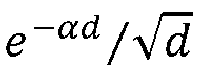
distinctive knee 109 on the log-log scale. The guidedfield strength curve 103 and the radiatedfield strength curve 106 intersect at point 112, which occurs at a crossing distance. At distances less than the crossing distance at intersection point 112, the field strength of a guided electromagnetic field is significantly greater at most locations than the field strength of a radiated electromagnetic field. At distances greater than the crossing distance, the opposite is true. Thus, the guided and radiated field strength curves 103 and 106 further illustrate the fundamental propagation difference between guided and radiated electromagnetic fields. For an informal discussion of the difference between guided and radiated electromagnetic fields, reference is made to Milligan, T., Modern Antenna Design, McGraw-Hill, 1st Edition, 1985, pp.8-9. - The distinction between radiated and guided electromagnetic waves, made above, is readily expressed formally and placed on a rigorous basis. That two such diverse solutions could emerge from one and the same linear partial differential equation, the wave equation, analytically follows from the boundary conditions imposed on the problem. The Green function for the wave equation, itself, contains the distinction between the nature of radiation and guided waves.
- In empty space, the wave equation is a differential operator whose eigenfunctions possess a continuous spectrum of eigenvalues on the complex wave-number plane. This transverse electro-magnetic (TEM) field is called the radiation field, and those propagating fields are called "Hertzian waves." However, in the presence of a conducting boundary, the wave equation plus boundary conditions mathematically lead to a spectral representation of wave-numbers composed of a continuous spectrum plus a sum of discrete spectra. To this end, reference is made to Sommerfeld, A., "Uber die Ausbreitung der Wellen in der Drahtlosen Telegraphie," Annalen der Physik, Vol. 28, 1909, pp. 665-736. Also see Sommerfeld, A., "Problems of Radio," published as Chapter 6 in Partial Differential Equations in Physics - Lectures on Theoretical Physics: Volume VI, Academic Press, 1949, pp. 236-289, 295-296; Collin, R. E., "Hertzian Dipole Radiating Over a Lossy Earth or Sea: Some Early and Late 20th Century Controversies," IEEE Antennas and Propagation Magazine, Vol. 46, No. 2, April 2004, pp. 64-79; and Reich, H. J., Ordnung, P.F, Krauss, H.L., and Skalnik, J.G., Microwave Theory and Techniques, Van Nostrand, 1953, pp. 291-293.
- The terms "ground wave" and "surface wave" identify two distinctly different physical propagation phenomena. A surface wave arises analytically from a distinct pole yielding a discrete component in the plane wave spectrum. See, e.g., "The Excitation of Plane Surface Waves" by Cullen, A.L., (Proceedings of the IEE (British), Vol. 101, Part IV, August 1954, pp. 225-235). In this context, a surface wave is considered to be a guided surface wave. The surface wave (in the Zenneck-Sommerfeld guided wave sense) is, physically and mathematically, not the same as the ground wave (in the Weyl-Norton-FCC sense) that is now so familiar from radio broadcasting. These two propagation mechanisms arise from the excitation of different types of eigenvalue spectra (continuum or discrete) on the complex plane. The field strength of the guided surface wave decays exponentially with distance as illustrated by
curve 103 ofFIG. 1 (much like propagation in a lossy waveguide) and resembles propagation in a radial transmission line, as opposed to the classical Hertzian radiation of the ground wave, which propagates spherically, possesses a continuum of eigenvalues, falls off geometrically as illustrated bycurve 106 ofFIG. 1 , and results from branch-cut integrals. As experimentally demonstrated by C.R. Burrows in "The Surface Wave in Radio Propagation over Plane Earth" (Proceedings of the IRE, Vol. 25, No. 2, February, 1937, pp. 219-229) and "The Surface Wave in Radio Transmission" (Bell Laboratories Record, Vol. 15, June 1937, pp. 321-324), vertical antennas radiate ground waves but do not launch guided surface waves. - To summarize the above, first, the continuous part of the wave-number eigenvalue spectrum, corresponding to branch-cut integrals, produces the radiation field, and second, the discrete spectra, and corresponding residue sum arising from the poles enclosed by the contour of integration, result in non-TEM traveling surface waves that are exponentially damped in the direction transverse to the propagation. Such surface waves are guided transmission line modes. For further explanation, reference is made to Friedman, B., Principles and Techniques of Applied Mathematics, Wiley, 1956, pp. pp. 214, 283-286, 290, 298-300.
- In free space, antennas excite the continuum eigenvalues of the wave equation, which is a radiation field, where the outwardly propagating RF energy with Ez and Hφ in-phase is lost forever. On the other hand, waveguide probes excite discrete eigenvalues, which results in transmission line propagation. See Collin, R. E., Field Theory of Guided Waves, McGraw-Hill, 1960, pp. 453, 474-477. While such theoretical analyses have held out the hypothetical possibility of launching open surface guided waves over planar or spherical surfaces of lossy, homogeneous media, for more than a century no known structures in the engineering arts have existed for accomplishing this with any practical efficiency. Unfortunately, since it emerged in the early 1900's, the theoretical analysis set forth above has essentially remained a theory and there have been no known structures for practically accomplishing the launching of open surface guided waves over planar or spherical surfaces of lossy, homogeneous media.
- According to the various embodiments of the present disclosure, various guided surface waveguide probes are described that are configured to excite electric fields that couple into a guided surface waveguide mode along the surface of a lossy conducting medium. Such guided electromagnetic fields are substantially mode-matched in magnitude and phase to a guided surface wave mode on the surface of the lossy conducting medium. Such a guided surface wave mode can also be termed a Zenneck waveguide mode. By virtue of the fact that the resultant fields excited by the guided surface waveguide probes described herein are substantially mode-matched to a guided surface waveguide mode on the surface of the lossy conducting medium, a guided electromagnetic field in the form of a guided surface wave is launched along the surface of the lossy conducting medium. According to one embodiment, the lossy conducting medium comprises a terrestrial medium such as the Earth.
- Referring to
FIG. 2 , shown is a propagation interface that provides for an examination of the boundary value solutions to Maxwell's equations derived in 1907 by Jonathan Zenneck as set forth in his paper Zenneck, J., "On the Propagation of Plane Electromagnetic Waves Along a Flat Conducting Surface and their Relation to Wireless Telegraphy," Annalen der Physik, Serial 4, Vol. 23, September 20, 1907, pp. 846-866.FIG. 2 depicts cylindrical coordinates for radially propagating waves along the interface between a lossy conducting medium specified asRegion 1 and an insulator specified asRegion 2.Region 1 can comprise, for example, any lossy conducting medium. In one example, such a lossy conducting medium can comprise a terrestrial medium such as the Earth or other medium.Region 2 is a second medium that shares a boundary interface withRegion 1 and has different constitutive parameters relative toRegion 1.Region 2 can comprise, for example, any insulator such as the atmosphere or other medium. The reflection coefficient for such a boundary interface goes to zero only for incidence at a complex Brewster angle. See Stratton, J.A., Electromagnetic Theory, McGraw-Hill, 1941, p. 516. - According to various embodiments, the present disclosure sets forth various guided surface waveguide probes that generate electromagnetic fields that are substantially mode-matched to a guided surface waveguide mode on the surface of the lossy conducting
medium comprising Region 1. According to various embodiments, such electromagnetic fields substantially synthesize a wave front incident at a complex Brewster angle of the lossy conducting medium that can result in zero reflection. - To explain further, in
Region 2, where an ejωt field variation is assumed and where ρ = 0 and z ≥ 0 (with z being the vertical coordinate normal to the surface ofRegion 1, and ρ being the radial dimension in cylindrical coordinates), Zenneck's closed-form exact solution of Maxwell's equations satisfying the boundary conditions along the interface are expressed by the following electric field and magnetic field components:


- In
Region 1, where the ejωt field variation is assumed and where ρ ≠ 0 and z ≤ 0, Zenneck's closed-form exact solution of Maxwell's equations satisfying the boundary conditions along the interface is expressed by the following electric field and magnetic field components:


- In these expressions, z is the vertical coordinate normal to the surface of
Region 1 and ρ is the radial coordinate,
Region 1, u 2 is the propagation constant in the vertical (z) direction inRegion 2, σ 1 is the conductivity ofRegion 1, ω is equal to 2πf, where f is a frequency of excitation, εo is the permittivity of free space, ε 1 is the permittivity ofRegion 1, A is a source constant imposed by the source, and γ is a surface wave radial propagation constant. - The propagation constants in the ±z directions are determined by separating the wave equation above and below the interface between
Regions Region 2,
Region 1,


Region 1, σ 1 is the conductivity ofRegion 1, εo is the permittivity of free space, and µo comprises the permeability of free space. Thus, the generated surface wave propagates parallel to the interface and exponentially decays vertical to it. This is known as evanescence. - Thus, Equations (1)-(3) can be considered to be a cylindrically-symmetric, radially-propagating waveguide mode. See Barlow, H. M., and Brown, J., Radio Surface Waves, Oxford University Press, 1962, pp. 10-12, 29-33. The present disclosure details structures that excite this "open boundary" waveguide mode. Specifically, according to various embodiments, a guided surface waveguide probe is provided with a charge terminal of appropriate size that is fed with voltage and/or current and is positioned relative to the boundary interface between
Region 2 andRegion 1. This may be better understood with reference toFIG. 3 , which shows an example of a guidedsurface waveguide probe 200a that includes a charge terminal T1 elevated above a lossy conducting medium 203 (e.g., the Earth) along a vertical axis z that is normal to a plane presented by thelossy conducting medium 203. Thelossy conducting medium 203 makes upRegion 1, and asecond medium 206 makes upRegion 2 and shares a boundary interface with thelossy conducting medium 203. - According to one embodiment, the lossy conducting medium 203 can comprise a terrestrial medium such as the planet Earth. To this end, such a terrestrial medium comprises all structures or formations included thereon whether natural or man-made. For example, such a terrestrial medium can comprise natural elements such as rock, soil, sand, fresh water, sea water, trees, vegetation, and all other natural elements that make up our planet. In addition, such a terrestrial medium can comprise man-made elements such as concrete, asphalt, building materials, and other man-made materials. In other embodiments, the lossy conducting medium 203 can comprise some medium other than the Earth, whether naturally occurring or man-made. In other embodiments, the lossy conducting medium 203 can comprise other media such as man-made surfaces and structures such as automobiles, aircraft, man-made materials (such as plywood, plastic sheeting, or other materials) or other media.
- In the case where the
lossy conducting medium 203 comprises a terrestrial medium or Earth, thesecond medium 206 can comprise the atmosphere above the ground. As such, the atmosphere can be termed an "atmospheric medium" that comprises air and other elements that make up the atmosphere of the Earth. In addition, it is possible that thesecond medium 206 can comprise other media relative to thelossy conducting medium 203. - The guided
surface waveguide probe 200a includes afeed network 209 that couples anexcitation source 212 to the charge terminal T1 via, e.g., a vertical feed line conductor. According to various embodiments, a charge Q1 is imposed on the charge terminal T1 to synthesize an electric field based upon the voltage applied to terminal T1 at any given instant. Depending on the angle of incidence (θi ) of the electric field (E), it is possible to substantially mode-match the electric field to a guided surface waveguide mode on the surface of the lossy conducting medium 203 comprisingRegion 1. - By considering the Zenneck closed-form solutions of Equations (1)-(6), the Leontovich impedance boundary condition between
Region 1 andRegion 2 can be stated as

Region 2 expressed by Equation (1) above. Equation (13) implies that the electric and magnetic fields specified in Equations (1)-(3) may result in a radial surface current density along the boundary interface, where the radial surface current density can be specified by

FIG. 3 , the "close-in" ground current flows radially inward. By field matching on Hφ "close-in," it can be determined that

- At this point, a review of the nature of the Hankel functions used in Equations (1)-(6) and (17) is provided for these solutions of the wave equation. One might observe that the Hankel functions of the first and second kind and order n are defined as complex combinations of the standard Bessel functions of the first and second kinds


outward 
- That


- Thus, beyond the Hankel crossover point the "far out" representation predominates over the "close-in" representation of the Hankel function. The distance to the Hankel crossover point (or Hankel crossover distance) can be found by equating Equations (20b) and (21) for -jyp, and solving for Rx. With x = σ/ωεo, it can be seen that the far-out and close-in Hankel function asymptotes are frequency dependent, with the Hankel crossover point moving out as the frequency is lowered. It should also be noted that the Hankel function asymptotes may also vary as the conductivity (σ) of the lossy conducting medium changes. For example, the conductivity of the soil can vary with changes in weather conditions.
- Referring to
FIG. 4 , shown is an example of a plot of the magnitudes of the first order Hankel functions of Equations (20b) and (21) for aRegion 1 conductivity of σ = 0.010 mhos/m and relative permittivity εr = 15, at an operating frequency of 1850 kHz.Curve 115 is the magnitude of the far-out asymptote of Equation (20b) andcurve 118 is the magnitude of the close-in asymptote of Equation (21), with theHankel crossover point 121 occurring at a distance of Rx = 54 feet. While the magnitudes are equal, a phase offset exists between the two asymptotes at theHankel crossover point 121. It can also be seen that the Hankel crossover distance is much less than a wavelength of the operation frequency. - Considering the electric field components given by Equations (2) and (3) of the Zenneck closed-form solution in
Region 2, it can be seen that the ratio of Ez and Eρ asymptotically passes to

- For example, the height H1 of the elevated charge terminal T1 in
FIG. 3 affects the amount of free charge on the charge terminal T1. When the charge terminal T1 is near the ground plane ofRegion 1, most of the charge Q1 on the terminal is "bound." As the charge terminal T1 is elevated, the bound charge is lessened until the charge terminal T1 reaches a height at which substantially all of the isolated charge is free. - The advantage of an increased capacitive elevation for the charge terminal T1 is that the charge on the elevated charge terminal T1 is further removed from the ground plane, resulting in an increased amount of free charge qfree to couple energy into the guided surface waveguide mode. As the charge terminal T1 is moved away from the ground plane, the charge distribution becomes more uniformly distributed about the surface of the terminal. The amount of free charge is related to the self-capacitance of the charge terminal T1.
- For example, the capacitance of a spherical terminal can be expressed as a function of physical height above the ground plane. The capacitance of a sphere at a physical height of h above a perfect ground is given by

- In the case of a sufficiently isolated terminal, the self-capacitance of a conductive sphere can be approximated by C = 4πεoa, where a is the radius of the sphere in meters, and the self-capacitance of a disk can be approximated by C = 8εoa, where a is the radius of the disk in meters. The charge terminal T1 can include any shape such as a sphere, a disk, a cylinder, a cone, a torus, a hood, one or more rings, or any other randomized shape or combination of shapes. An equivalent spherical diameter can be determined and used for positioning of the charge terminal T1.
- This may be further understood with reference to the example of
FIG. 3 , where the charge terminal T1 is elevated at a physical height of hp = H1 above thelossy conducting medium 203. To reduce the effects of the "bound" charge, the charge terminal T1 can be positioned at a physical height that is at least four times the spherical diameter (or equivalent spherical diameter) of the charge terminal T1 to reduce the bounded charge effects. - Referring next to
FIG. 5A , shown is a ray optics interpretation of the electric field produced by the elevated charge Q1 on charge terminal T1 ofFIG. 3 . As in optics, minimizing the reflection of the incident electric field can improve and/or maximize the energy coupled into the guided surface waveguide mode of thelossy conducting medium 203. For an electric field (E ∥) that is polarized parallel to the plane of incidence (not the boundary interface), the amount of reflection of the incident electric field may be determined using the Fresnel reflection coefficient, which can be expressed as
- In the example of
FIG. 5A , the ray optic interpretation shows the incident field polarized parallel to the plane of incidence having an angle of incidence of θi , which is measured with respect to the surface normal (ẑ). There will be no reflection of the incident electric field when Γ∥(θi ) = 0 and thus the incident electric field will be completely coupled into a guided surface waveguide mode along the surface of thelossy conducting medium 203. It can be seen that the numerator of Equation (25) goes to zero when the angle of incidence is
- As illustrated in
FIG. 5A , the electric field vector E can be depicted as an incoming non-uniform plane wave, polarized parallel to the plane of incidence. The electric field vector E can be created from independent horizontal and vertical components as
FIG. 5A suggests that the electric field vector E can be given by


- A generalized parameter W, called "wave tilt," is noted herein as the ratio of the horizontal electric field component to the vertical electric field component given by


Region 2, the wave tilt angle (Ψ) is equal to the angle between the normal of the wave-front at the boundary interface withRegion 1 and the tangent to the boundary interface. This may be easier to see inFIG. 5B , which illustrates equi-phase surfaces of an electromagnetic wave and their normals for a radial cylindrical guided surface wave. At the boundary interface (z = 0) with a perfect conductor, the wave-front normal is parallel to the tangent of the boundary interface, resulting in W = 0. However, in the case of a lossy dielectric, a wave tilt W exists because the wave-front normal is not parallel with the tangent of the boundary interface at z = 0. - Applying Equation (30b) to a guided surface wave gives


- The concept of an electrical effective height can provide further insight into synthesizing an electric field with a complex angle of incidence with a guided surface waveguide probe 200. The electrical effective height (heff ) has been defined as


FIG. 3 , IC is the current that is distributed along the vertical structure of the guidedsurface waveguide probe 200a. - For example, consider a
feed network 209 that includes a low loss coil (e.g., a helical coil) at the bottom of the structure and a vertical feed line conductor connected between the coil and the charge terminal T1. The phase delay due to the coil (or helical delay line) is θc = βplC , with a physical length of lC and a propagation factor of
- In addition, the spatial phase delay along the length lw of the vertical feed line conductor can be given by θy = βwlw where βw is the propagation phase constant for the vertical feed line conductor. In some implementations, the spatial phase delay may be approximated by θy = βwhp, since the difference between the physical height hp of the guided
surface waveguide probe 200a and the vertical feed line conductor length lw is much less than a wavelength at the supplied frequency (λ 0). As a result, the total phase delay through the coil and vertical feed line conductor is Φ = θc + θy, and the current fed to the top of the coil from the bottom of the physical structure is

lossy conducting medium 203. - In the example of
FIG. 5A , ray optics are used to illustrate the complex angle trigonometry of the incident electric field (E) having a complex Brewster angle of incidence (θi,B ) at the Hankel crossover distance (Rx ) 121. Recall from Equation (26) that, for a lossy conducting medium, the Brewster angle is complex and specified by


- In
FIG. 5A , a right triangle is depicted having an adjacent side of length Rx along the lossy conducting medium surface and a complex Brewster angle ψi,B measured between aray 124 extending between theHankel crossover point 121 at Rx and the center of the charge terminal T1, and the lossy conductingmedium surface 127 between theHankel crossover point 121 and the charge terminal T1. With the charge terminal T1 positioned at physical height hp and excited with a charge having the appropriate phase delay Φ, the resulting electric field is incident with the lossy conducting medium boundary interface at the Hankel crossover distance Rx , and at the Brewster angle. Under these conditions, the guided surface waveguide mode can be excited without reflection or substantially negligible reflection. - If the physical height of the charge terminal T1 is decreased without changing the phase shift Φ of the effective height (heff ), the resulting electric field intersects the lossy conducting medium 203 at the Brewster angle at a reduced distance from the guided surface waveguide probe 200.
FIG. 6 graphically illustrates the effect of decreasing the physical height of the charge terminal T1 on the distance where the electric field is incident at the Brewster angle. As the height is decreased from h3 through h2 to h1, the point where the electric field intersects with the lossy conducting medium (e.g., the Earth) at the Brewster angle moves closer to the charge terminal position. However, as Equation (39) indicates, the height H1 (FIG. 3 ) of the charge terminal T1 should be at or higher than the physical height (hp ) in order to excite the far-out component of the Hankel function. With the charge terminal T1 positioned at or above the effective height (heff ), the lossy conducting medium 203 can be illuminated at the Brewster angle of incidence (ψi,B = (π/2) - θi,B ) at or beyond the Hankel crossover distance (Rx ) 121 as illustrated inFIG. 5A . To reduce or minimize the bound charge on the charge terminal T1, the height should be at least four times the spherical diameter (or equivalent spherical diameter) of the charge terminal T1 as mentioned above. - A guided surface waveguide probe 200 can be configured to establish an electric field having a wave tilt that corresponds to a wave illuminating the surface of the lossy conducting medium 203 at a complex Brewster angle, thereby exciting radial surface currents by substantially mode-matching to a guided surface wave mode at (or beyond) the
Hankel crossover point 121 at Rx. - Referring to
FIG. 7 , shown is a graphical representation of an example of a guidedsurface waveguide probe 200b that includes a charge terminal T1.An AC source 212 acts as the excitation source for the charge terminal T1, which is coupled to the guidedsurface waveguide probe 200b through a feed network 209 (FIG. 3 ) comprising acoil 215 such as, e.g., a helical coil. In other implementations, theAC source 212 can be inductively coupled to thecoil 215 through a primary coil. In some embodiments, an impedance matching network may be included to improve and/or maximize coupling of theAC source 212 to thecoil 215. - As shown in
FIG. 7 , the guidedsurface waveguide probe 200b can include the upper charge terminal T1 (e.g., a sphere at height hp ) that is positioned along a vertical axis z that is substantially normal to the plane presented by thelossy conducting medium 203. Asecond medium 206 is located above thelossy conducting medium 203. The charge terminal T1 has a self-capacitance CT. During operation, charge Q1 is imposed on the terminal T1 depending on the voltage applied to the terminal T1 at any given instant. - In the example of
FIG. 7 , thecoil 215 is coupled to aground stake 218 at a first end and to the charge terminal T1 via a verticalfeed line conductor 221. In some implementations, the coil connection to the charge terminal T1 can be adjusted using atap 224 of thecoil 215 as shown inFIG. 7 . Thecoil 215 can be energized at an operating frequency by theAC source 212 through atap 227 at a lower portion of thecoil 215. In other implementations, theAC source 212 can be inductively coupled to thecoil 215 through a primary coil. - The construction and adjustment of the guided surface waveguide probe 200 is based upon various operating conditions, such as the transmission frequency, conditions of the lossy conducting medium (e.g., soil conductivity σ and relative permittivity εr ), and size of the charge terminal T1. The index of refraction can be calculated from Equations (10) and (11) as

lossy conducting medium 203. The complex Brewster angle (θi,B ) measured from the surface normal can also be determined from Equation (26) as
FIG. 5A as
- The Hankel crossover distance can also be found by equating the magnitudes of Equations (20b) and (21) for -jyp, and solving for Rx as illustrated by
FIG. 4 . The electrical effective height can then be determined from Equation (39) using the Hankel crossover distance and the complex Brewster angle as
- With the charge terminal T1 positioned at or above the physical height (hp ), the feed network 209 (
FIG. 3 ) and/or the vertical feed line connecting the feed network to the charge terminal T1 can be adjusted to match the phase (Φ) of the charge Q1 on the charge terminal T1 to the angle (Ψ) of the wave tilt (W). The size of the charge terminal T1 can be chosen to provide a sufficiently large surface for the charge Q1 imposed on the terminals. In general, it is desirable to make the charge terminal T1 as large as practical. The size of the charge terminal T1 should be large enough to avoid ionization of the surrounding air, which can result in electrical discharge or sparking around the charge terminal. - The phase delay θc of a helically-wound coil can be determined from Maxwell's equations as has been discussed by Corum, K.L. and J.F. Corum, "RF Coils, Helical Resonators and Voltage Magnification by Coherent Spatial Modes," Microwave Review, Vol. 7, No. 2, September 2001, pp. 36-45. For a helical coil with H/D > 1, the ratio of the velocity of propagation (v) of a wave along the coil's longitudinal axis to the speed of light (c), or the "velocity factor," is given by


- The spatial phase delay θy of the structure can be determined using the traveling wave phase delay of the vertical feed line conductor 221 (
FIG. 7 ). The capacitance of a cylindrical vertical conductor above a prefect ground plane can be expressed as


- With a charge terminal T1 positioned over the lossy conducting medium 203 as shown in
FIG. 3 , thefeed network 209 can be adjusted to excite the charge terminal T1 with the phase shift (Φ) of the complex effective height (heff ) equal to the angle (Ψ) of the wave tilt at the Hankel crossover distance, or Φ = Ψ. When this condition is met, the electric field produced by the charge oscillating Q1 on the charge terminal T1 is coupled into a guided surface waveguide mode traveling along the surface of alossy conducting medium 203. For example, if the Brewster angle (θi,B ), the phase delay (θy ) associated with the vertical feed line conductor 221 (FIG. 7 ), and the configuration of the coil 215 (FIG. 7 ) are known, then the position of the tap 224 (FIG. 7 ) can be determined and adjusted to impose an oscillating charge Q1 on the charge terminal T1 with phase Φ = Ψ. The position of thetap 224 may be adjusted to maximize coupling the traveling surface waves into the guided surface waveguide mode. Excess coil length beyond the position of thetap 224 can be removed to reduce the capacitive effects. The vertical wire height and/or the geometrical parameters of the helical coil may also be varied. - The coupling to the guided surface waveguide mode on the surface of the lossy conducting medium 203 can be improved and/or optimized by tuning the guided surface waveguide probe 200 for standing wave resonance with respect to a complex image plane associated with the charge Q1 on the charge terminal T1. By doing this, the performance of the guided surface waveguide probe 200 can be adjusted for increased and/or maximum voltage (and thus charge Q1) on the charge terminal T1. Referring back to
FIG. 3 , the effect of the lossy conducting medium 203 inRegion 1 can be examined using image theory analysis. - Physically, an elevated charge Q1 placed over a perfectly conducting plane attracts the free charge on the perfectly conducting plane, which then "piles up" in the region under the elevated charge Q1. The resulting distribution of "bound" electricity on the perfectly conducting plane is similar to a bell-shaped curve. The superposition of the potential of the elevated charge Q1, plus the potential of the induced "piled up" charge beneath it, forces a zero equipotential surface for the perfectly conducting plane. The boundary value problem solution that describes the fields in the region above the perfectly conducting plane may be obtained using the classical notion of image charges, where the field from the elevated charge is superimposed with the field from a corresponding "image" charge below the perfectly conducting plane.
- This analysis may also be used with respect to a
lossy conducting medium 203 by assuming the presence of an effective image charge Q1' beneath the guided surface waveguide probe 200. The effective image charge Q1' coincides with the charge Q1 on the charge terminal T1 about a conductingimage ground plane 130, as illustrated inFIG. 3 . However, the image charge Q1' is not merely located at some real depth and 180° out of phase with the primary source charge Q1 on the charge terminal T1, as they would be in the case of a perfect conductor. Rather, the lossy conducting medium 203 (e.g., a terrestrial medium) presents a phase shifted image. That is to say, the image charge Q1' is at a complex depth below the surface (or physical boundary) of thelossy conducting medium 203. For a discussion of complex image depth, reference is made to Wait, J. R., "Complex Image Theory-Revisited," IEEE Antennas and Propagation Magazine, Vol. 33, No. 4, August 1991, pp. 27-29. - Instead of the image charge Q1' being at a depth that is equal to the physical height (H1) of the charge Q1, the conducting image ground plane 130 (representing a perfect conductor) is located at a complex depth of z = - d/2 and the image charge Q1' appears at a complex depth (i.e., the "depth" has both magnitude and phase), given by -D1 = -(d/2 + d/2 + H1) ≠ H1. For vertically polarized sources over the Earth,


image ground plane 130 at z = - d/2, and not at the boundary interface betweenRegions - Consider the case illustrated in
FIG. 8A where thelossy conducting medium 203 is a finitely conductingEarth 133 with aphysical boundary 136. The finitely conductingEarth 133 may be replaced by a perfectly conductingimage ground plane 139 as shown inFIG.8B , which is located at a complex depth z 1 below thephysical boundary 136. This equivalent representation exhibits the same impedance when looking down into the interface at thephysical boundary 136. The equivalent representation ofFIG. 8B can be modeled as an equivalent transmission line, as shown inFIG. 8C . The cross-section of the equivalent structure is represented as a (z-directed) end-loaded transmission line, with the impedance of the perfectly conducting image plane being a short circuit (zs = 0). The depth z 1 can be determined by equating the TEM wave impedance looking down at the Earth to an image ground plane impedance zin seen looking into the transmission line ofFIG. 8C . - In the case of
FIG. 8A , the propagation constant and wave intrinsic impedance in the upper region (air) 142 are

lossy Earth 133, the propagation constant and wave intrinsic impedance are

FIG. 8B is equivalent to a TEM transmission line whose characteristic impedance is that of air (zo ), with propagation constant of γ o , and whose length is z 1. As such, the image ground plane impedance Zin seen at the interface for the shorted transmission line ofFIG. 8C is given by
FIG. 8C to the normal incidence wave impedance ofFIG. 8A and solving for z 1 gives the distance to a short circuit (the perfectly conducting image ground plane 139) as
air region 142, the propagation constant is γo = jβo, so Zin = jZo tan βoz 1 (which is a purely imaginary quantity for a real z 1), but ze is a complex value if σ ≠ 0. Therefore, Zin = Ze only when z 1 is a complex distance. - Since the equivalent representation of
FIG. 8B includes a perfectly conductingimage ground plane 139, the image depth for a charge or current lying at the surface of the Earth (physical boundary 136) is equal to distance z 1 on the other side of theimage ground plane 139, or d = 2 × z 1 beneath the Earth's surface (which is located at z = 0). Thus, the distance to the perfectly conductingimage ground plane 139 can be approximated by
image ground plane 139 at depth z 1 = - d/2 will be zero. - If a charge Q1 is elevated a distance H1 above the surface of the Earth as illustrated in
FIG. 3 , then the image charge Q1' resides at a complex distance of D1 = d + H1 below the surface, or a complex distance of d/2 + H1 below theimage ground plane 130. The guidedsurface waveguide probe 200b ofFIG. 7 can be modeled as an equivalent single-wire transmission line image plane model that can be based upon the perfectly conductingimage ground plane 139 ofFIG. 8B .FIG. 9A shows an example of the equivalent single-wire transmission line image plane model, andFIG. 9B illustrates an example of the equivalent classic transmission line model, including the shorted transmission line ofFIG. 8C . - In the equivalent image plane models of
FIGS. 9A and 9B , Φ = θy + θc is the traveling wave phase delay of the guided surface waveguide probe 200 referenced to Earth 133 (or the lossy conducting medium 203), θc = βpH is the electrical length of the coil 215 (FIG. 7 ), of physical length H, expressed in degrees, θy = βwhw is the electrical length of the vertical feed line conductor 221 (FIG. 7 ), of physical length hw, expressed in degrees, and θd = βo d/2 is the phase shift between theimage ground plane 139 and thephysical boundary 136 of the Earth 133 (or lossy conducting medium 203). In the example ofFIGS. 9A and 9B , Zw is the characteristic impedance of the elevated verticalfeed line conductor 221 in ohms, Zc is the characteristic impedance of thecoil 215 in ohms, and ZO is the characteristic impedance of free space. - At the base of the guided surface waveguide probe 200, the impedance seen "looking up" into the structure is Z ↑ = Zbase . With a load impedance of:

FIG. 7 ) is given by:
FIG. 7 ) is given by:
lossy conducting medium 203 is Z ↓ = Zin , which is given by:
- Neglecting losses, the equivalent image plane model can be tuned to resonance when Z ↓ + Z ↑ = 0 at the
physical boundary 136. Or, in the low loss case, X ↓ + X ↑ = 0 at thephysical boundary 136, where X is the corresponding reactive component. Thus, the impedance at thephysical boundary 136 "looking up" into the guided surface waveguide probe 200 is the conjugate of the impedance at thephysical boundary 136 "looking down" into thelossy conducting medium 203. By adjusting the load impedance ZL of the charge terminal T1 while maintaining the traveling wave phase delay Φ equal to the angle of the media's wave tilt Ψ, so that Φ = Ψ, which improves and/or maximizes coupling of the probe's electric field to a guided surface waveguide mode along the surface of the lossy conducting medium 203 (e.g., Earth), the equivalent image plane models ofFIGS. 9A and 9B can be tuned to resonance with respect to theimage ground plane 139. In this way, the impedance of the equivalent complex image plane model is purely resistive, which maintains a superposed standing wave on the probe structure that maximizes the voltage and elevated charge on terminal T1 , and by equations (1)-(3) and (16) maximizes the propagating surface wave. - It follows from the Hankel solutions, that the guided surface wave excited by the guided surface waveguide probe 200 is an outward propagating traveling wave. The source distribution along the
feed network 209 between the charge terminal T1 and theground stake 218 of the guided surface waveguide probe 200 (FIGS. 3 and7 ) is actually composed of a superposition of a traveling wave plus a standing wave on the structure. With the charge terminal T1 positioned at or above the physical height hp, the phase delay of the traveling wave moving through thefeed network 209 is matched to the angle of the wave tilt associated with thelossy conducting medium 203. This mode-matching allows the traveling wave to be launched along thelossy conducting medium 203. Once the phase delay has been established for the traveling wave, the load impedance ZL of the charge terminal T1 is adjusted to bring the probe structure into standing wave resonance with respect to the image ground plane (130 ofFIG. 3 or 139 ofFIG. 8 ), which is at a complex depth of - d/2. In that case, the impedance seen from the image ground plane has zero reactance and the charge on the charge terminal T1 is maximized. - The distinction between the traveling wave phenomenon and standing wave phenomena is that (1) the phase delay of traveling waves (θ = βd) on a section of transmission line of length d (sometimes called a "delay line") is due to propagation time delays; whereas (2) the position-dependent phase of standing waves (which are composed of forward and backward propagating waves) depends on both the line length propagation time delay and impedance transitions at interfaces between line sections of different characteristic impedances. In addition to the phase delay that arises due to the physical length of a section of transmission line operating in sinusoidal steady-state, there is an extra reflection coefficient phase at impedance discontinuities that is due to the ratio of Zoa /Zob , where Zoa and Zob are the characteristic impedances of two sections of a transmission line such as, e.g., a helical coil section of characteristic impedance Zoa = Zc (
FIG. 9B ) and a straight section of vertical feed line conductor of characteristic impedance Zob = Zw (FIG. 9B ). - As a result of this phenomenon, two relatively short transmission line sections of widely differing characteristic impedance may be used to provide a very large phase shift. For example, a probe structure composed of two sections of transmission line, one of low impedance and one of high impedance, together totaling a physical length of, say, 0.05 λ, may be fabricated to provide a phase shift of 90° which is equivalent to a 0.25 λ resonance. This is due to the large jump in characteristic impedances. In this way, a physically short probe structure can be electrically longer than the two physical lengths combined. This is illustrated in
FIGS. 9A and 9B , where the discontinuities in the impedance ratios provide large jumps in phase. The impedance discontinuity provides a substantial phase shift where the sections are joined together. - Referring to
FIG. 10 , shown is aflow chart 150 illustrating an example of adjusting a guided surface waveguide probe 200 (FIGS. 3 and7 ) to substantially mode-match to a guided surface waveguide mode on the surface of the lossy conducting medium, which launches a guided surface traveling wave along the surface of a lossy conducting medium 203 (FIG. 3 ). Beginning with 153, the charge terminal T1 of the guided surface waveguide probe 200 is positioned at a defined height above alossy conducting medium 203. Utilizing the characteristics of thelossy conducting medium 203 and the operating frequency of the guided surface waveguide probe 200, the Hankel crossover distance can also be found by equating the magnitudes of Equations (20b) and (21) for -jyp, and solving for Rx as illustrated byFIG. 4 . The complex index of refraction (n) can be determined using Equation (41), and the complex Brewster angle (θi,B ) can then be determined from Equation (42). The physical height (hp ) of the charge terminal T1 can then be determined from Equation (44). The charge terminal T1 should be at or higher than the physical height (hp ) in order to excite the far-out component of the Hankel function. This height relationship is initially considered when launching surface waves. To reduce or minimize the bound charge on the charge terminal T1, the height should be at least four times the spherical diameter (or equivalent spherical diameter) of the charge terminal T1. - At 156, the electrical phase delay Φ of the elevated charge Q1 on the charge terminal T1 is matched to the complex wave tilt angle Ψ. The phase delay (θc ) of the helical coil and/or the phase delay (θy ) of the vertical feed line conductor can be adjusted to make Φ equal to the angle (Ψ) of the wave tilt (W). Based on Equation (31), the angle (Ψ) of the wave tilt can be determined from:

FIG. 7 ) and/or the length (or height) of the vertical feed line conductor 221 (FIG. 7 ). By matching Φ = Ψ, an electric field can be established at or beyond the Hankel crossover distance (Rx ) with a complex Brewster angle at the boundary interface to excite the surface waveguide mode and launch a traveling wave along thelossy conducting medium 203. - Next at 159, the load impedance of the charge terminal T1 is tuned to resonate the equivalent image plane model of the guided surface waveguide probe 200. The depth (d/2) of the conducting
image ground plane 139 ofFIG. 9A and 9B (or 130 ofFIG. 3 ) can be determined using Equations (52), (53) and (54) and the values of the lossy conducting medium 203 (e.g., the Earth), which can be measured. Using that depth, the phase shift (θd ) between theimage ground plane 139 and thephysical boundary 136 of the lossy conducting medium 203 can be determined using θd = βo d/2. The impedance (Zin ) as seen "looking down" into the lossy conducting medium 203 can then be determined using Equation (65). This resonance relationship can be considered to maximize the launched surface waves. - Based upon the adjusted parameters of the
coil 215 and the length of the verticalfeed line conductor 221, the velocity factor, phase delay, and impedance of thecoil 215 and verticalfeed line conductor 221 can be determined using Equations (45) through (51). In addition, the self-capacitance (CT ) of the charge terminal T1 can be determined using, e.g., Equation (24). The propagation factor (βp ) of thecoil 215 can be determined using Equation (35) and the propagation phase constant (βw ) for the verticalfeed line conductor 221 can be determined using Equation (49). Using the self-capacitance and the determined values of thecoil 215 and verticalfeed line conductor 221, the impedance (Zbase ) of the guided surface waveguide probe 200 as seen "looking up" into thecoil 215 can be determined using Equations (62), (63) and (64). - The equivalent image plane model of the guided surface waveguide probe 200 can be tuned to resonance by adjusting the load impedance ZL such that the reactance component Xbase of Zbase cancels out the reactance component Xin of Zin , or Xbase + Xin = 0. Thus, the impedance at the
physical boundary 136 "looking up" into the guided surface waveguide probe 200 is the conjugate of the impedance at thephysical boundary 136 "looking down" into thelossy conducting medium 203. The load impedance ZL can be adjusted by varying the capacitance (CT ) of the charge terminal T1 without changing the electrical phase delay Φ = θc + θy of the charge terminal T1. An iterative approach may be taken to tune the load impedance ZL for resonance of the equivalent image plane model with respect to the conducting image ground plane 139 (or 130). In this way, the coupling of the electric field to a guided surface waveguide mode along the surface of the lossy conducting medium 203 (e.g., Earth) can be improved and/or maximized. - This may be better understood by illustrating the situation with a numerical example. Consider a guided surface waveguide probe 200 comprising a top-loaded vertical stub of physical height hp with a charge terminal T1 at the top, where the charge terminal T1 is excited through a helical coil and vertical feed line conductor at an operational frequency (fo ) of 1.85 MHz. With a height (H1) of 16 feet and the lossy conducting medium 203 (e.g., Earth) having a relative permittivity of εr = 15 and a conductivity of σ 1 = 0.010 mhos/m, several surface wave propagation parameters can be calculated for fo = 1.850 MHz. Under these conditions, the Hankel crossover distance can be found to be Rx = 54.5 feet with a physical height of hp = 5.5 feet, which is well below the actual height of the charge terminal T1. While a charge terminal height of H1 = 5.5 feet could have been used, the taller probe structure reduced the bound capacitance, permitting a greater percentage of free charge on the charge terminal T1 providing greater field strength and excitation of the traveling wave.
- The wave length can be determined as:


- The velocity factor of the vertical feed line conductor (approximated as a uniform cylindrical conductor with a diameter of 0.27 inches) can be given as Vw ≈ 0.93. Since hp << λo , the propagation phase constant for the vertical feed line conductor can be approximated as:


FIG. 11 shows a plot of both over a range of frequencies. As both Φ and Ψ are frequency dependent, it can be seen that their respective curves cross over each other at approximately 1.85 MHz. - For a helical coil having a conductor diameter of 0.0881 inches, a coil diameter (D) of 30 inches and a turn-to-turn spacing (s) of 4 inches, the velocity factor for the coil can be determined using Equation (45) as:


- With the traveling wave phase delay of the coil and vertical feed line conductor adjusted to match the wave tilt angle (Φ = θc + θy = Ψ), the load impedance (ZL ) of the charge terminal T1 can be adjusted for standing wave resonance of the equivalent image plane model of the guided surface wave probe 200. From the measured permittivity, conductivity and permeability of the Earth, the radial propagation constant can be determined using Equation (57)


- By matching the reactive component (Xin ) seen "looking down" into the lossy conducting medium 203 with the reactive component (Xbase ) seen "looking up" into the guided surface wave probe 200, the coupling into the guided surface waveguide mode may be maximized. This can be accomplished by adjusting the capacitance of the charge terminal T1 without changing the traveling wave phase delays of the coil and vertical feed line conductor. For example, by adjusting the charge terminal capacitance (CT ) to 61.8126 pF, the load impedance from Equation (62) is:

- Using Equation (51), the impedance of the vertical feed line conductor (having a diameter (2a) of 0.27 inches) is given as


FIGS. 9A and 9B from the perfectly conducting image ground plane is only resistive or Zip = R + j0. - When the electric fields produced by a guided surface waveguide probe 200 (
FIG. 3 ) are established by matching the traveling wave phase delay of the feed network to the wave tilt angle and the probe structure is resonated with respect to the perfectly conducting image ground plane at complex depth z = -d/2, the fields are substantially mode-matched to a guided surface waveguide mode on the surface of the lossy conducting medium, a guided surface traveling wave is launched along the surface of the lossy conducting medium. As illustrated inFIG. 1 , the guidedfield strength curve 103 of the guided electromagnetic field has a characteristic exponential decay of
distinctive knee 109 on the log-log scale. - In summary, both analytically and experimentally, the traveling wave component on the structure of the guided surface waveguide probe 200 has a phase delay (Φ) at its upper terminal that matches the angle (Ψ) of the wave tilt of the surface traveling wave (Φ = Ψ). Under this condition, the surface waveguide may be considered to be "mode-matched". Furthermore, the resonant standing wave component on the structure of the guided surface waveguide probe 200 has a VMAX at the charge terminal T1 and a VMIN down at the image plane 139 (
FIG. 8B ) where Zip = Rip +j 0 at a complex depth of z = - d/2, not at the connection at thephysical boundary 136 of the lossy conducting medium 203 (FIG. 8B ). Lastly, the charge terminal T1 is of sufficient height H1 ofFIG. 3 (h ≥ Rx tan ψ i,B ) so that electromagnetic waves incident onto the lossy conducting medium 203 at the complex Brewster angle do so out at a distance (≥ Rx ) where the
- Referring back to
FIG. 3 , operation of a guided surface waveguide probe 200 may be controlled to adjust for variations in operational conditions associated with the guided surface waveguide probe 200. For example, an adaptiveprobe control system 230 can be used to control thefeed network 209 and/or the charge terminal T1 to control the operation of the guided surface waveguide probe 200. Operational conditions can include, but are not limited to, variations in the characteristics of the lossy conducting medium 203 (e.g., conductivity σ and relative permittivity εr ), variations in field strength and/or variations in loading of the guided surface waveguide probe 200. As can be seen from Equations (31), (41) and (42), the index of refraction (n), the complex Brewster angle (θi,B ), and the wave tilt (|W|e jΨ) can be affected by changes in soil conductivity and permittivity resulting from, e.g., weather conditions. - Equipment such as, e.g., conductivity measurement probes, permittivity sensors, ground parameter meters, field meters, current monitors and/or load receivers can be used to monitor for changes in the operational conditions and provide information about current operational conditions to the adaptive
probe control system 230. Theprobe control system 230 can then make one or more adjustments to the guided surface waveguide probe 200 to maintain specified operational conditions for the guided surface waveguide probe 200. For instance, as the moisture and temperature vary, the conductivity of the soil will also vary. Conductivity measurement probes and/or permittivity sensors may be located at multiple locations around the guided surface waveguide probe 200. Generally, it would be desirable to monitor the conductivity and/or permittivity at or about the Hankel crossover distance Rx for the operational frequency. Conductivity measurement probes and/or permittivity sensors may be located at multiple locations (e.g., in each quadrant) around the guided surface waveguide probe 200. - The conductivity measurement probes and/or permittivity sensors can be configured to evaluate the conductivity and/or permittivity on a periodic basis and communicate the information to the
probe control system 230. The information may be communicated to theprobe control system 230 through a network such as, but not limited to, a LAN, WLAN, cellular network, or other appropriate wired or wireless communication network. Based upon the monitored conductivity and/or permittivity, theprobe control system 230 may evaluate the variation in the index of refraction (n), the complex Brewster angle (θi,B ), and/or the wave tilt (|W|e jΨ) and adjust the guided surface waveguide probe 200 to maintain the phase delay (Φ) of thefeed network 209 equal to the wave tilt angle (Ψ) and/or maintain resonance of the equivalent image plane model of the guided surface waveguide probe 200. This can be accomplished by adjusting, e.g., θ y, θ c and/or CT. For instance, theprobe control system 230 can adjust the self-capacitance of the charge terminal T1 and/or the phase delay (θ y , θ c ) applied to the charge terminal T1 to maintain the electrical launching efficiency of the guided surface wave at or near its maximum. For example, the self-capacitance of the charge terminal T1 can be varied by changing the size of the terminal. The charge distribution can also be improved by increasing the size of the charge terminal T1, which can reduce the chance of an electrical discharge from the charge terminal T1. In other embodiments, the charge terminal T1 can include a variable inductance that can be adjusted to change the load impedance ZL . The phase applied to the charge terminal T1 can be adjusted by varying the tap position on the coil 215 (FIG. 7 ), and/or by including a plurality of predefined taps along thecoil 215 and switching between the different predefined tap locations to maximize the launching efficiency. - Field or field strength (FS) meters may also be distributed about the guided surface waveguide probe 200 to measure field strength of fields associated with the guided surface wave. The field or FS meters can be configured to detect the field strength and/or changes in the field strength (e.g., electric field strength) and communicate that information to the
probe control system 230. The information may be communicated to theprobe control system 230 through a network such as, but not limited to, a LAN, WLAN, cellular network, or other appropriate communication network. As the load and/or environmental conditions change or vary during operation, the guided surface waveguide probe 200 may be adjusted to maintain specified field strength(s) at the FS meter locations to ensure appropriate power transmission to the receivers and the loads they supply. - For example, the phase delay (Φ = θ y + θ c ) applied to the charge terminal T1 can be adjusted to match the wave tilt angle (Ψ). By adjusting one or both phase delays, the guided surface waveguide probe 200 can be adjusted to ensure the wave tilt corresponds to the complex Brewster angle. This can be accomplished by adjusting a tap position on the coil 215 (
FIG. 7 ) to change the phase delay supplied to the charge terminal T1. The voltage level supplied to the charge terminal T1 can also be increased or decreased to adjust the electric field strength. This may be accomplished by adjusting the output voltage of theexcitation source 212 or by adjusting or reconfiguring thefeed network 209. For instance, the position of the tap 227 (FIG. 7 ) for theAC source 212 can be adjusted to increase the voltage seen by the charge terminal T1. Maintaining field strength levels within predefined ranges can improve coupling by the receivers, reduce ground current losses, and avoid interference with transmissions from other guided surface waveguide probes 200. - The
probe control system 230 can be implemented with hardware, firmware, software executed by hardware, or a combination thereof. For example, theprobe control system 230 can include processing circuitry including a processor and a memory, both of which can be coupled to a local interface such as, for example, a data bus with an accompanying control/address bus as can be appreciated by those with ordinary skill in the art. A probe control application may be executed by the processor to adjust the operation of the guided surface waveguide probe 200 based upon monitored conditions. Theprobe control system 230 can also include one or more network interfaces for communicating with the various monitoring devices. Communications can be through a network such as, but not limited to, a LAN, WLAN, cellular network, or other appropriate communication network. Theprobe control system 230 may comprise, for example, a computer system such as a server, desktop computer, laptop, or other system with like capability. - Referring back to the example of
FIG. 5A , the complex angle trigonometry is shown for the ray optic interpretation of the incident electric field (E) of the charge terminal T1 with a complex Brewster angle (θi,B ) at the Hankel crossover distance (Rx ). Recall that, for a lossy conducting medium, the Brewster angle is complex and specified by equation (38). Electrically, the geometric parameters are related by the electrical effective height (heff ) of the charge terminal T1 by equation (39). Since both the physical height (hp ) and the Hankel crossover distance (Rx ) are real quantities, the angle of the desired guided surface wave tilt at the Hankel crossover distance (WRx ) is equal to the phase (Φ) of the complex effective height (heff ). With the charge terminal T1 positioned at the physical height hp and excited with a charge having the appropriate phase Φ, the resulting electric field is incident with the lossy conducting medium boundary interface at the Hankel crossover distance Rx , and at the Brewster angle. Under these conditions, the guided surface waveguide mode can be excited without reflection or substantially negligible reflection. - However, Equation (39) means that the physical height of the guided surface waveguide probe 200 can be relatively small. While this will excite the guided surface waveguide mode, this can result in an unduly large bound charge with little free charge. To compensate, the charge terminal T1 can be raised to an appropriate elevation to increase the amount of free charge. As one example rule of thumb, the charge terminal T1 can be positioned at an elevation of about 4-5 times (or more) the effective diameter of the charge terminal T1.
FIG. 6 illustrates the effect of raising the charge terminal T1 above the physical height (hp ) shown inFIG. 5A . The increased elevation causes the distance at which the wave tilt is incident with the lossy conductive medium to move beyond the Hankel crossover point 121 (FIG. 5A ). To improve coupling in the guided surface waveguide mode, and thus provide for a greater launching efficiency of the guided surface wave, a lower compensation terminal T2 can be used to adjust the total effective height (hTE ) of the charge terminal T1 such that the wave tilt at the Hankel crossover distance is at the Brewster angle. - Referring to
FIG. 12 , shown is an example of a guidedsurface waveguide probe 200c that includes an elevated charge terminal T1 and a lower compensation terminal T2 that are arranged along a vertical axis z that is normal to a plane presented by thelossy conducting medium 203. In this respect, the charge terminal T1 is placed directly above the compensation terminal T2 although it is possible that some other arrangement of two or more charge and/or compensation terminals TN can be used. The guidedsurface waveguide probe 200c is disposed above alossy conducting medium 203 according to an embodiment of the present disclosure. Thelossy conducting medium 203 makes upRegion 1 with asecond medium 206 that makes upRegion 2 sharing a boundary interface with thelossy conducting medium 203. - The guided
surface waveguide probe 200c includes afeed network 209 that couples anexcitation source 212 to the charge terminal T1 and the compensation terminal T2. According to various embodiments, charges Q1 and Q2 can be imposed on the respective charge and compensation terminals T1 and T2, depending on the voltages applied to terminals T1 and T2 at any given instant. I1 is the conduction current feeding the charge Q1 on the charge terminal T1 via the terminal lead, and I2 is the conduction current feeding the charge Q2 on the compensation terminal T2 via the terminal lead. - According to the embodiment of
FIG. 12 , the charge terminal T1 is positioned over the lossy conducting medium 203 at a physical height H1, and the compensation terminal T2 is positioned directly below T1 along the vertical axis z at a physical height H2, where H2 is less than H1. The height h of the transmission structure may be calculated as h = H1 - H2. The charge terminal T1 has an isolated (or self) capacitance C1, and the compensation terminal T2 has an isolated (or self) capacitance C2. A mutual capacitance CM can also exist between the terminals T1 and T2 depending on the distance therebetween. During operation, charges Q1 and Q2 are imposed on the charge terminal T1 and the compensation terminal T2, respectively, depending on the voltages applied to the charge terminal T1 and the compensation terminal T2 at any given instant. - Referring next to
FIG. 13 , shown is a ray optics interpretation of the effects produced by the elevated charge Q1 on charge terminal T1 and compensation terminal T2 ofFIG. 12 . With the charge terminal T1 elevated to a height where the ray intersects with the lossy conductive medium at the Brewster angle at a distance greater than theHankel crossover point 121 as illustrated byline 163, the compensation terminal T2 can be used to adjust hTE by compensating for the increased height. The effect of the compensation terminal T2 is to reduce the electrical effective height of the guided surface waveguide probe (or effectively raise the lossy medium interface) such that the wave tilt at the Hankel crossover distance is at the Brewster angle as illustrated byline 166. - The total effective height can be written as the superposition of an upper effective height (hUE ) associated with the charge terminal T1 and a lower effective height (hLE ) associated with the compensation terminal T2 such that


FIG. 5A . - Equations (85) or (86) can be used to determine the physical height of the lower disk of the compensation terminal T2 and the phase angles to feed the terminals in order to obtain the desired wave tilt at the Hankel crossover distance. For example, Equation (86) can be rewritten as the phase shift applied to the charge terminal T1 as a function of the compensation terminal height (hd ) to give

- To determine the positioning of the compensation terminal T2, the relationships discussed above can be utilized. First, the total effective height (hTE ) is the superposition of the complex effective height (hUE ) of the upper charge terminal T1 and the complex effective height (hLE ) of the lower compensation terminal T2 as expressed in Equation (86). Next, the tangent of the angle of incidence can be expressed geometrically as

Hankel crossover point 121. This can be accomplished by adjusting hp, Φ U , and/or hd. - These concepts may be better understood when discussed in the context of an example of a guided surface waveguide probe. Referring to
FIG. 14 , shown is a graphical representation of an example of a guidedsurface waveguide probe 200d including an upper charge terminal T1 (e.g., a sphere at height hT ) and a lower compensation terminal T2 (e.g., a disk at height hd ) that are positioned along a vertical axis z that is substantially normal to the plane presented by thelossy conducting medium 203. During operation, charges Q1 and Q2 are imposed on the charge and compensation terminals T1 and T2, respectively, depending on the voltages applied to the terminals T1 and T2 at any given instant. - An
AC source 212 acts as the excitation source for the charge terminal T1, which is coupled to the guidedsurface waveguide probe 200d through afeed network 209 comprising acoil 215 such as, e.g., a helical coil. TheAC source 212 can be connected across a lower portion of thecoil 215 through atap 227, as shown inFIG. 14 , or can be inductively coupled to thecoil 215 by way of a primary coil. Thecoil 215 can be coupled to aground stake 218 at a first end and the charge terminal T1 at a second end. In some implementations, the connection to the charge terminal T1 can be adjusted using atap 224 at the second end of thecoil 215. The compensation terminal T2 is positioned above and substantially parallel with the lossy conducting medium 203 (e.g., the ground or Earth), and energized through atap 233 coupled to thecoil 215. Anammeter 236 located between thecoil 215 andground stake 218 can be used to provide an indication of the magnitude of the current flow (I 0) at the base of the guided surface waveguide probe. Alternatively, a current clamp may be used around the conductor coupled to theground stake 218 to obtain an indication of the magnitude of the current flow (I 0). - In the example of
FIG. 14 , thecoil 215 is coupled to aground stake 218 at a first end and the charge terminal T1 at a second end via a verticalfeed line conductor 221. In some implementations, the connection to the charge terminal T1 can be adjusted using atap 224 at the second end of thecoil 215 as shown inFIG. 14 . Thecoil 215 can be energized at an operating frequency by theAC source 212 through atap 227 at a lower portion of thecoil 215. In other implementations, theAC source 212 can be inductively coupled to thecoil 215 through a primary coil. The compensation terminal T2 is energized through atap 233 coupled to thecoil 215. Anammeter 236 located between thecoil 215 andground stake 218 can be used to provide an indication of the magnitude of the current flow at the base of the guidedsurface waveguide probe 200d. Alternatively, a current clamp may be used around the conductor coupled to theground stake 218 to obtain an indication of the magnitude of the current flow. The compensation terminal T2 is positioned above and substantially parallel with the lossy conducting medium 203 (e.g., the ground). - In the example of
FIG. 14 , the connection to the charge terminal T1 located on thecoil 215 above the connection point oftap 233 for the compensation terminal T2. Such an adjustment allows an increased voltage (and thus a higher charge Q1) to be applied to the upper charge terminal T1. In other embodiments, the connection points for the charge terminal T1 and the compensation terminal T2 can be reversed. It is possible to adjust the total effective height (hTE ) of the guidedsurface waveguide probe 200d to excite an electric field having a guided surface wave tilt at the Hankel crossover distance Rx. The Hankel crossover distance can also be found by equating the magnitudes of equations (20b) and (21) for -jyp, and solving for Rx as illustrated byFIG. 4 . The index of refraction (n), the complex Brewster angle (θi,B and ψi,B ), the wave tilt (|W|e jΨ) and the complex effective height (heff = hpe jΦ) can be determined as described with respect to Equations (41) - (44) above. - With the selected charge terminal T1 configuration, a spherical diameter (or the effective spherical diameter) can be determined. For example, if the charge terminal T1 is not configured as a sphere, then the terminal configuration may be modeled as a spherical capacitance having an effective spherical diameter. The size of the charge terminal T1 can be chosen to provide a sufficiently large surface for the charge Q1 imposed on the terminals. In general, it is desirable to make the charge terminal T1 as large as practical. The size of the charge terminal T1 should be large enough to avoid ionization of the surrounding air, which can result in electrical discharge or sparking around the charge terminal. To reduce the amount of bound charge on the charge terminal T1, the desired elevation to provide free charge on the charge terminal T1 for launching a guided surface wave should be at least 4-5 times the effective spherical diameter above the lossy conductive medium (e.g., the Earth). The compensation terminal T2 can be used to adjust the total effective height (hTE ) of the guided
surface waveguide probe 200d to excite an electric field having a guided surface wave tilt at Rx. The compensation terminal T2 can be positioned below the charge terminal T1 at hd = hT - hp, where hT is the total physical height of the charge terminal T1. With the position of the compensation terminal T2 fixed and the phase delay Φ U applied to the upper charge terminal T1, the phase delay Φ L applied to the lower compensation terminal T2 can be determined using the relationships of Equation (86), such that:
FIG. 15A , which showsplots plot 172. At this fixed height, the coil phase Φ U can be determined from Re{Φ U }, as graphically illustrated inplot 175. - With the
AC source 212 coupled to the coil 215 (e.g., at the 50Ω point to maximize coupling), the position oftap 233 may be adjusted for parallel resonance of the compensation terminal T2 with at least a portion of the coil at the frequency of operation.FIG. 15B shows a schematic diagram of the general electrical hookup ofFIG. 14 in which V1 is the voltage applied to the lower portion of thecoil 215 from theAC source 212 throughtap 227, V2 is the voltage attap 224 that is supplied to the upper charge terminal T1, and V3 is the voltage applied to the lower compensation terminal T2 throughtap 233. The resistances Rp and Rd represent the ground return resistances of the charge terminal T1 and compensation terminal T2, respectively. The charge and compensation terminals T1 and T2 may be configured as spheres, cylinders, toroids, rings, hoods, or any other combination of capacitive structures. The size of the charge and compensation terminals T1 and T2 can be chosen to provide a sufficiently large surface for the charges Q1 and Q2 imposed on the terminals. In general, it is desirable to make the charge terminal T1 as large as practical. The size of the charge terminal T1 should be large enough to avoid ionization of the surrounding air, which can result in electrical discharge or sparking around the charge terminal. The self-capacitance Cp and Cd of the charge and compensation terminals T1 and T2 respectively, can be determined using, for example, equation (24). - As can be seen in
FIG. 15B , a resonant circuit is formed by at least a portion of the inductance of thecoil 215, the self-capacitance Cd of the compensation terminal T2, and the ground return resistance Rd associated with the compensation terminal T2. The parallel resonance can be established by adjusting the voltage V3 applied to the compensation terminal T2 (e.g., by adjusting atap 233 position on the coil 215) or by adjusting the height and/or size of the compensation terminal T2 to adjust Cd. The position of thecoil tap 233 can be adjusted for parallel resonance, which will result in the ground current through theground stake 218 and through theammeter 236 reaching a maximum point. After parallel resonance of the compensation terminal T2 has been established, the position of thetap 227 for theAC source 212 can be adjusted to the 50Ω point on thecoil 215. - Voltage V2 from the
coil 215 can be applied to the charge terminal T1, and the position oftap 224 can be adjusted such that the phase (Φ) of the total effective height (hTE ) approximately equals the angle of the guided surface wave tilt (WRx ) at the Hankel crossover distance (Rx ). The position of thecoil tap 224 can be adjusted until this operating point is reached, which results in the ground current through theammeter 236 increasing to a maximum. At this point, the resultant fields excited by the guidedsurface waveguide probe 200d are substantially mode-matched to a guided surface waveguide mode on the surface of thelossy conducting medium 203, resulting in the launching of a guided surface wave along the surface of thelossy conducting medium 203. This can be verified by measuring field strength along a radial extending from the guided surface waveguide probe 200. - Resonance of the circuit including the compensation terminal T2 may change with the attachment of the charge terminal T1 and/or with adjustment of the voltage applied to the charge terminal T1 through
tap 224. While adjusting the compensation terminal circuit for resonance aids the subsequent adjustment of the charge terminal connection, it is not necessary to establish the guided surface wave tilt (WRx ) at the Hankel crossover distance (Rx ). The system may be further adjusted to improve coupling by iteratively adjusting the position of thetap 227 for theAC source 212 to be at the 50Ω point on thecoil 215 and adjusting the position oftap 233 to maximize the ground current through theammeter 236. Resonance of the circuit including the compensation terminal T2 may drift as the positions oftaps coil 215. - In other implementations, the voltage V2 from the
coil 215 can be applied to the charge terminal T1, and the position oftap 233 can be adjusted such that the phase (Φ) of the total effective height (hTE ) approximately equals the angle (Ψ) of the guided surface wave tilt at Rx. The position of thecoil tap 224 can be adjusted until the operating point is reached, resulting in the ground current through theammeter 236 substantially reaching a maximum. The resultant fields are substantially mode-matched to a guided surface waveguide mode on the surface of thelossy conducting medium 203, and a guided surface wave is launched along the surface of thelossy conducting medium 203. This can be verified by measuring field strength along a radial extending from the guided surface waveguide probe 200. The system may be further adjusted to improve coupling by iteratively adjusting the position of thetap 227 for theAC source 212 to be at the 50Ω point on thecoil 215 and adjusting the position oftap 224 and/or 233 to maximize the ground current through theammeter 236. - Referring back to
FIG. 12 , operation of a guided surface waveguide probe 200 may be controlled to adjust for variations in operational conditions associated with the guided surface waveguide probe 200. For example, aprobe control system 230 can be used to control thefeed network 209 and/or positioning of the charge terminal T1 and/or compensation terminal T2 to control the operation of the guided surface waveguide probe 200. Operational conditions can include, but are not limited to, variations in the characteristics of the lossy conducting medium 203 (e.g., conductivity σ and relative permittivity εr ), variations in field strength and/or variations in loading of the guided surface waveguide probe 200. As can be seen from Equations (41) - (44), the index of refraction (n), the complex Brewster angle (θi,B and ψi,B ), the wave tilt (|W|e jΨ) and the complex effective height (heff = hpe jΦ) can be affected by changes in soil conductivity and permittivity resulting from, e.g., weather conditions. - Equipment such as, e.g., conductivity measurement probes, permittivity sensors, ground parameter meters, field meters, current monitors and/or load receivers can be used to monitor for changes in the operational conditions and provide information about current operational conditions to the
probe control system 230. Theprobe control system 230 can then make one or more adjustments to the guided surface waveguide probe 200 to maintain specified operational conditions for the guided surface waveguide probe 200. For instance, as the moisture and temperature vary, the conductivity of the soil will also vary. Conductivity measurement probes and/or permittivity sensors may be located at multiple locations around the guided surface waveguide probe 200. Generally, it would be desirable to monitor the conductivity and/or permittivity at or about the Hankel crossover distance Rx for the operational frequency. Conductivity measurement probes and/or permittivity sensors may be located at multiple locations (e.g., in each quadrant) around the guided surface waveguide probe 200. - With reference then to
FIG. 16 , shown is an example of a guidedsurface waveguide probe 200e that includes a charge terminal T1 and a charge terminal T2 that are arranged along a vertical axis z. The guidedsurface waveguide probe 200e is disposed above alossy conducting medium 203, which makes upRegion 1. In addition, a second medium 206 shares a boundary interface with thelossy conducting medium 203 and makes upRegion 2. The charge terminals T1 and T2 are positioned over thelossy conducting medium 203. The charge terminal T1 is positioned at height H1, and the charge terminal T2 is positioned directly below T1 along the vertical axis z at height H2, where H2 is less than H1. The height h of the transmission structure presented by the guidedsurface waveguide probe 200e is h = H1 - H2. The guidedsurface waveguide probe 200e includes afeed network 209 that couples anexcitation source 212 to the charge terminals T1 and T2. - The charge terminals T1 and/or T2 include a conductive mass that can hold an electrical charge, which may be sized to hold as much charge as practically possible. The charge terminal T1 has a self-capacitance C1, and the charge terminal T2 has a self-capacitance C2, which can be determined using, for example, equation (24). By virtue of the placement of the charge terminal T1 directly above the charge terminal T2, a mutual capacitance CM is created between the charge terminals T1 and T2. Note that the charge terminals T1 and T2 need not be identical, but each can have a separate size and shape, and can include different conducting materials. Ultimately, the field strength of a guided surface wave launched by a guided
surface waveguide probe 200e is directly proportional to the quantity of charge on the terminal T1. The charge Q1 is, in turn, proportional to the self-capacitance C1 associated with the charge terminal T1 since Q1 = C1V, where V is the voltage imposed on the charge terminal T1. - When properly adjusted to operate at a predefined operating frequency, the guided
surface waveguide probe 200e generates a guided surface wave along the surface of thelossy conducting medium 203. Theexcitation source 212 can generate electrical energy at the predefined frequency that is applied to the guidedsurface waveguide probe 200e to excite the structure. When the electromagnetic fields generated by the guidedsurface waveguide probe 200e are substantially mode-matched with thelossy conducting medium 203, the electromagnetic fields substantially synthesize a wave front incident at a complex Brewster angle that results in little or no reflection. Thus, thesurface waveguide probe 200e does not produce a radiated wave, but launches a guided surface traveling wave along the surface of alossy conducting medium 203. The energy from theexcitation source 212 can be transmitted as Zenneck surface currents to one or more receivers that are located within an effective transmission range of the guidedsurface waveguide probe 200e. - One can determine asymptotes of the radial Zenneck surface current Jρ (ρ) on the surface of the lossy conducting medium 203 to be J 1(ρ) close-in and J 2(ρ) far-out, where


- The asymptotes representing the radial current close-in and far-out as set forth by equations (90) and (91) are complex quantities. According to various embodiments, a physical surface current J( ρ ), is synthesized to match as close as possible the current asymptotes in magnitude and phase. That is to say close-in, |J( ρ )| is to be tangent to |J 1|, and far-out |J( ρ )| is to be tangent to |J 2|. Also, according to the various embodiments, the phase of J( ρ ) should transition from the phase of J 1 close-in to the phase of J 2 far-out.
- In order to match the guided surface wave mode at the site of transmission to launch a guided surface wave, the phase of the surface current |J 2|far-out should differ from the phase of the surface current |J 1| close-in by the propagation phase corresponding to e -jβ(ρ
2 -(ρ1 ) plus a constant of approximately 45 degrees or 225 degrees. This is because there are two roots for


- In order to obtain the appropriate voltage magnitudes and phases for a given design of a guided
surface waveguide probe 200e at a given location, an iterative approach may be used. Specifically, analysis may be performed of a given excitation and configuration of a guidedsurface waveguide probe 200e taking into account the feed currents to the terminals T1 and T2, the charges on the charge terminals T1 and T2, and their images in the lossy conducting medium 203 in order to determine the radial surface current density generated. This process may be performed iteratively until an optimal configuration and excitation for a given guidedsurface waveguide probe 200e is determined based on desired parameters. To aid in determining whether a given guidedsurface waveguide probe 200e is operating at an optimal level, a guided field strength curve 103 (FIG. 1 ) may be generated using equations (1)-(12) based on values for the conductivity of Region 1 (σ 1) and the permittivity of Region 1 (ε 1) at the location of the guidedsurface waveguide probe 200e. Such a guidedfield strength curve 103 can provide a benchmark for operation such that measured field strengths can be compared with the magnitudes indicated by the guidedfield strength curve 103 to determine if optimal transmission has been achieved. - In order to arrive at an optimized condition, various parameters associated with the guided
surface waveguide probe 200e may be adjusted. One parameter that may be varied to adjust the guidedsurface waveguide probe 200e is the height of one or both of the charge terminals T1 and/or T2 relative to the surface of thelossy conducting medium 203. In addition, the distance or spacing between the charge terminals T1 and T2 may also be adjusted. In doing so, one may minimize or otherwise alter the mutual capacitance CM or any bound capacitances between the charge terminals T1 and T2 and the lossy conducting medium 203 as can be appreciated. The size of the respective charge terminals T1 and/or T2 can also be adjusted. By changing the size of the charge terminals T1 and/or T2, one will alter the respective self-capacitances C1 and/or C2, and the mutual capacitance CM as can be appreciated. - Still further, another parameter that can be adjusted is the
feed network 209 associated with the guidedsurface waveguide probe 200e. This may be accomplished by adjusting the size of the inductive and/or capacitive reactances that make up thefeed network 209. For example, where such inductive reactances comprise coils, the number of turns on such coils may be adjusted. Ultimately, the adjustments to thefeed network 209 can be made to alter the electrical length of thefeed network 209, thereby affecting the voltage magnitudes and phases on the charge terminals T1 and T2. - Note that the iterations of transmission performed by making the various adjustments may be implemented by using computer models or by adjusting physical structures as can be appreciated. By making the above adjustments, one can create corresponding "close-in" surface current J 1 and "far-out" surface current J 2 that approximate the same currents J( ρ ) of the guided surface wave mode specified in Equations (90) and (91) set forth above. In doing so, the resulting electromagnetic fields would be substantially or approximately mode-matched to a guided surface wave mode on the surface of the
lossy conducting medium 203. - While not shown in the example of
FIG. 16 , operation of the guidedsurface waveguide probe 200e may be controlled to adjust for variations in operational conditions associated with the guided surface waveguide probe 200. For example, aprobe control system 230 shown inFIG. 12 can be used to control thefeed network 209 and/or positioning and/or size of the charge terminals T1 and/or T2 to control the operation of the guidedsurface waveguide probe 200e. Operational conditions can include, but are not limited to, variations in the characteristics of the lossy conducting medium 203 (e.g., conductivity σ and relative permittivity εr ), variations in field strength and/or variations in loading of the guidedsurface waveguide probe 200e. - Referring now to
FIG. 17 , shown is an example of the guidedsurface waveguide probe 200e ofFIG. 16 , denoted herein as guidedsurface waveguide probe 200f. The guidedsurface waveguide probe 200f includes the charge terminals T1 and T2 that are positioned along a vertical axis z that is substantially normal to the plane presented by the lossy conducting medium 203 (e.g., the Earth). Thesecond medium 206 is above thelossy conducting medium 203. The charge terminal T1 has a self-capacitance C1, and the charge terminal T2 has a self-capacitance C2. During operation, charges Q1 and Q2 are imposed on the charge terminals T1 and T2, respectively, depending on the voltages applied to the charge terminals T1 and T2 at any given instant. A mutual capacitance CM may exist between the charge terminals T1 and T2 depending on the distance there between. In addition, bound capacitances may exist between the respective charge terminals T1 and T2 and the lossy conducting medium 203 depending on the heights of the respective charge terminals T1 and T2 with respect to thelossy conducting medium 203. - The guided
surface waveguide probe 200f includes afeed network 209 that comprises an inductive impedance comprising a coil L1a having a pair of leads that are coupled to respective ones of the charge terminals T1 and T2. In one embodiment, the coil L1a is specified to have an electrical length that is one-half (½) of the wavelength at the operating frequency of the guidedsurface waveguide probe 200f. - While the electrical length of the coil L1a is specified as approximately one-half (1/2) the wavelength at the operating frequency, it is understood that the coil L1a may be specified with an electrical length at other values. According to one embodiment, the fact that the coil L1a has an electrical length of approximately one-half the wavelength at the operating frequency provides for an advantage in that a maximum voltage differential is created on the charge terminals T1 and T2. Nonetheless, the length or diameter of the coil L1a may be increased or decreased when adjusting the guided
surface waveguide probe 200f to obtain optimal excitation of a guided surface wave mode. Adjustment of the coil length may be provided by taps located at one or both ends of the coil. In other embodiments, it may be the case that the inductive impedance is specified to have an electrical length that is significantly less than or greater than ½ the wavelength at the operating frequency of the guidedsurface waveguide probe 200f. - The
excitation source 212 can be coupled to thefeed network 209 by way of magnetic coupling. Specifically, theexcitation source 212 is coupled to a coil LP that is inductively coupled to the coil L1a. This may be done by link coupling, a tapped coil, a variable reactance, or other coupling approach as can be appreciated. To this end, the coil LP acts as a primary, and the coil L1a acts as a secondary as can be appreciated. - In order to adjust the guided
surface waveguide probe 200f for the transmission of a desired guided surface wave, the heights of the respective charge terminals T1 and T2 may be altered with respect to thelossy conducting medium 203 and with respect to each other. Also, the sizes of the charge terminals T1 and T2 may be altered. In addition, the size of the coil L1a may be altered by adding or eliminating turns or by changing some other dimension of the coil L1a. The coil L1a can also include one or more taps for adjusting the electrical length as shown inFIG. 17 . The position of a tap connected to either charge terminal T1 or T2 can also be adjusted. - Referring next to
FIGS. 18A, 18B ,18C and19 , shown are examples of generalized receive circuits for using the surface-guided waves in wireless power delivery systems.FIGS. 18A and18B-18C include alinear probe 303 and a tuned resonator 306, respectively.FIG. 19 is amagnetic coil 309 according to various embodiments of the present disclosure. According to various embodiments, each one of thelinear probe 303, the tuned resonator 306, and themagnetic coil 309 may be employed to receive power transmitted in the form of a guided surface wave on the surface of alossy conducting medium 203 according to various embodiments. As mentioned above, in one embodiment thelossy conducting medium 203 comprises a terrestrial medium (or Earth). - With specific reference to
FIG. 18A , the open-circuit terminal voltage at theoutput terminals 312 of thelinear probe 303 depends upon the effective height of thelinear probe 303. To this end, the terminal point voltage may be calculated as
linear probe 303 in Volts per meter, dl is an element of integration along the direction of thelinear probe 303, and he is the effective height of thelinear probe 303. Anelectrical load 315 is coupled to theoutput terminals 312 through animpedance matching network 318. - When the
linear probe 303 is subjected to a guided surface wave as described above, a voltage is developed across theoutput terminals 312 that may be applied to theelectrical load 315 through a conjugateimpedance matching network 318 as the case may be. In order to facilitate the flow of power to theelectrical load 315, theelectrical load 315 should be substantially impedance matched to thelinear probe 303 as will be described below. - Referring to
FIG. 18B , a ground currentexcited coil 306a possessing a phase shift equal to the wave tilt of the guided surface wave includes a charge terminal TR that is elevated (or suspended) above thelossy conducting medium 203. The charge terminal TR has a self-capacitance CR. In addition, there may also be a bound capacitance (not shown) between the charge terminal TR and the lossy conducting medium 203 depending on the height of the charge terminal TR above thelossy conducting medium 203. The bound capacitance should preferably be minimized as much as is practicable, although this may not be entirely necessary in every instance. - The
tuned resonator 306a also includes a receiver network comprising a coil LR having a phase shift Φ. One end of the coil LR is coupled to the charge terminal TR, and the other end of the coil LR is coupled to thelossy conducting medium 203. The receiver network can include a vertical supply line conductor that couples the coil LR to the charge terminal TR. To this end, the coil LR (which may also be referred to as tuned resonator LR-CR) comprises a series-adjusted resonator as the charge terminal CR and the coil LR are situated in series. The phase delay of the coil LR can be adjusted by changing the size and/or height of the charge terminal TR, and/or adjusting the size of the coil LR so that the phase Φ of the structure is made substantially equal to the angle of the wave tilt Ψ. The phase delay of the vertical supply line can also be adjusted by, e.g., changing length of the conductor. - For example, the reactance presented by the self-capacitance CR is calculated as 1/jωCR. Note that the total capacitance of the
structure 306a may also include capacitance between the charge terminal TR and thelossy conducting medium 203, where the total capacitance of thestructure 306a may be calculated from both the self-capacitance CR and any bound capacitance as can be appreciated. According to one embodiment, the charge terminal TR may be raised to a height so as to substantially reduce or eliminate any bound capacitance. The existence of a bound capacitance may be determined from capacitance measurements between the charge terminal TR and the lossy conducting medium 203 as previously discussed. - The inductive reactance presented by a discrete-element coil LR may be calculated as jωL, where L is the lumped-element inductance of the coil LR. If the coil LR is a distributed element, its equivalent terminal-point inductive reactance may be determined by conventional approaches. To tune the
structure 306a, one would make adjustments so that the phase delay is equal to the wave tilt for the purpose of mode-matching to the surface waveguide at the frequency of operation. Under this condition, the receiving structure may be considered to be "mode-matched" with the surface waveguide. A transformer link around the structure and/or animpedance matching network 324 may be inserted between the probe and theelectrical load 327 in order to couple power to the load. Inserting theimpedance matching network 324 between theprobe terminals 321 and theelectrical load 327 can effect a conjugate-match condition for maximum power transfer to theelectrical load 327. - When placed in the presence of surface currents at the operating frequencies power will be delivered from the surface guided wave to the
electrical load 327. To this end, anelectrical load 327 may be coupled to thestructure 306a by way of magnetic coupling, capacitive coupling, or conductive (direct tap) coupling. The elements of the coupling network may be lumped components or distributed elements as can be appreciated. - In the embodiment shown in
FIG. 18B , magnetic coupling is employed where a coil LS is positioned as a secondary relative to the coil LR that acts as a transformer primary. The coil LS may be link-coupled to the coil LR by geometrically winding it around the same core structure and adjusting the coupled magnetic flux as can be appreciated. In addition, while the receivingstructure 306a comprises a series-tuned resonator, a parallel-tuned resonator or even a distributed-element resonator of the appropriate phase delay may also be used. - While a receiving structure immersed in an electromagnetic field may couple energy from the field, it can be appreciated that polarization-matched structures work best by maximizing the coupling, and conventional rules for probe-coupling to waveguide modes should be observed. For example, a TE20 (transverse electric mode) waveguide probe may be optimal for extracting energy from a conventional waveguide excited in the TE20 mode. Similarly, in these cases, a mode-matched and phase-matched receiving structure can be optimized for coupling power from a surface-guided wave. The guided surface wave excited by a guided surface waveguide probe 200 on the surface of the lossy conducting medium 203 can be considered a waveguide mode of an open waveguide. Excluding waveguide losses, the source energy can be completely recovered. Useful receiving structures may be E-field coupled, H-field coupled, or surface-current excited.
- The receiving structure can be adjusted to increase or maximize coupling with the guided surface wave based upon the local characteristics of the lossy conducting medium 203 in the vicinity of the receiving structure. To accomplish this, the phase delay (Φ) of the receiving structure can be adjusted to match the angle (Ψ) of the wave tilt of the surface traveling wave at the receiving structure. If configured appropriately, the receiving structure may then be tuned for resonance with respect to the perfectly conducting image ground plane at complex depth z = -d/2.
- For example, consider a receiving structure comprising the tuned
resonator 306a ofFIG. 18B , including a coil LR and a vertical supply line connected between the coil LR and a charge terminal TR. With the charge terminal TR positioned at a defined height above thelossy conducting medium 203, the total phase shift Φ of the coil LR and vertical supply line can be matched with the angle (Ψ) of the wave tilt at the location of the tunedresonator 306a. From Equation (22), it can be seen that the wave tilt asymptotically passes to
- The total phase shift (Φ = θc + θy ) of the tuned
resonator 306a includes both the phase delay (θc ) through the coil LR and the phase delay of the vertical supply line (θy ). The spatial phase delay along the conductor length lw of the vertical supply line can be given by θy = βwlw, where βw is the propagation phase constant for the vertical supply line conductor. The phase delay due to the coil (or helical delay line) is θc = βplC, with a physical length of lC and a propagation factor of
FIG. 18B to adjust the coil phase delay (θc ) to match the total phase shift to the wave tilt angle (Φ = Ψ). For example, a portion of the coil can be bypassed by the tap connection as illustrated inFIG. 18B . The vertical supply line conductor can also be connected to the coil LR via a tap, whose position on the coil may be adjusted to match the total phase shift to the angle of the wave tilt. - Once the phase delay (Φ) of the tuned
resonator 306a has been adjusted, the impedance of the charge terminal TR can then be adjusted to tune to resonance with respect to the perfectly conducting image ground plane at complex depth z = -d/2. This can be accomplished by adjusting the capacitance of the charge terminal T1 without changing the traveling wave phase delays of the coil LR and vertical supply line. The adjustments are similar to those described with respect toFIGS. 9A and 9B . - The impedance seen "looking down" into the lossy conducting medium 203 to the complex image plane is given by:


lossy conducting medium 203 and ε 1 = εrεo. - At the base of the tuned
resonator 306a, the impedance seen "looking up" into the receiving structure is Z ↑ = Zbase as illustrated inFIG. 9A . With a terminal impedance of:
resonator 306a is given by:
resonator 306a is given by:
tuned resonator 306a, the coupling into the guided surface waveguide mode may be maximized. - Referring next to
FIG. 18C , shown is an example of atuned resonator 306b that does not include a charge terminal TR at the top of the receiving structure. In this embodiment, thetuned resonator 306b does not include a vertical supply line coupled between the coil LR and the charge terminal TR. Thus, the total phase shift (Φ) of thetuned resonator 306b includes only the phase delay (θc ) through the coil LR. As with thetuned resonator 306a ofFIG. 18B , the coil phase delay θc can be adjusted to match the angle (Ψ) of the wave tilt determined from Equation (97), which results in Φ = Ψ. While power extraction is possible with the receiving structure coupled into the surface waveguide mode, it is difficult to adjust the receiving structure to maximize coupling with the guided surface wave without the variable reactive load provided by the charge terminal TR. - Referring to
FIG. 18D , shown is aflow chart 180 illustrating an example of adjusting a receiving structure to substantially mode-match to a guided surface waveguide mode on the surface of thelossy conducting medium 203. Beginning with 181, if the receiving structure includes a charge terminal TR (e.g., of the tunedresonator 306a ofFIG. 18B ), then the charge terminal TR is positioned at a defined height above alossy conducting medium 203 at 184. As the surface guided wave has been established by a guided surface waveguide probe 200, the physical height (hp ) of the charge terminal TR may be below that of the effective height. The physical height may be selected to reduce or minimize the bound charge on the charge terminal TR (e.g., four times the spherical diameter of the charge terminal). If the receiving structure does not include a charge terminal TR (e.g., of thetuned resonator 306b ofFIG. 18C ), then the flow proceeds to 187. - At 187, the electrical phase delay Φ of the receiving structure is matched to the complex wave tilt angle Ψ defined by the local characteristics of the
lossy conducting medium 203. The phase delay (θc ) of the helical coil and/or the phase delay (θy ) of the vertical supply line can be adjusted to make Φ equal to the angle (Ψ) of the wave tilt (W). The angle (Ψ) of the wave tilt can be determined from Equation (86). The electrical phase Φ can then be matched to the angle of the wave tilt. For example, the electrical phase delay Φ = θc + θy can be adjusted by varying the geometrical parameters of the coil LR and/or the length (or height) of the vertical supply line conductor. - Next at 190, the load impedance of the charge terminal TR can be tuned to resonate the equivalent image plane model of the tuned
resonator 306a. The depth (d/2) of the conducting image ground plane 139 (FIG. 9A ) below the receiving structure can be determined using Equation (100) and the values of the lossy conducting medium 203 (e.g., the Earth) at the receiving structure, which can be locally measured. Using that complex depth, the phase shift (θd ) between theimage ground plane 139 and the physical boundary 136 (FIG. 9A ) of the lossy conducting medium 203 can be determined using θd = βo d/2. The impedance (Zin ) as seen "looking down" into the lossy conducting medium 203 can then be determined using Equation (99). This resonance relationship can be considered to maximize coupling with the guided surface waves. - Based upon the adjusted parameters of the coil LR and the length of the vertical supply line conductor, the velocity factor, phase delay, and impedance of the coil LR and vertical supply line can be determined. In addition, the self-capacitance (CR ) of the charge terminal TR can be determined using, e.g., Equation (24). The propagation factor (βp ) of the coil LR can be determined using Equation (98), and the propagation phase constant (βw ) for the vertical supply line can be determined using Equation (49). Using the self-capacitance and the determined values of the coil LR and vertical supply line, the impedance (Zbase ) of the tuned
resonator 306a as seen "looking up" into the coil LR can be determined using Equations (101), (102), and (103). - The equivalent image plane model of
FIG. 9A also applies to the tunedresonator 306a ofFIG. 18B . Thetuned resonator 306a can be tuned to resonance with respect to the complex image plane by adjusting the load impedance ZR of the charge terminal TR such that the reactance component Xbase of Zbase cancels out the reactance component of Xin of Zin, or Xbase + Xin = 0. Thus, the impedance at the physical boundary 136 (FIG. 9A ) "looking up" into the coil of the tunedresonator 306a is the conjugate of the impedance at thephysical boundary 136 "looking down" into thelossy conducting medium 203. The load impedance ZR can be adjusted by varying the capacitance (CR ) of the charge terminal TR without changing the electrical phase delay Φ = θc + θy seen by the charge terminal TR. An iterative approach may be taken to tune the load impedance ZR for resonance of the equivalent image plane model with respect to the conductingimage ground plane 139. In this way, the coupling of the electric field to a guided surface waveguide mode along the surface of the lossy conducting medium 203 (e.g., Earth) can be improved and/or maximized. - Referring to
FIG. 19 , themagnetic coil 309 comprises a receive circuit that is coupled through animpedance matching network 333 to anelectrical load 336. In order to facilitate reception and/or extraction of electrical power from a guided surface wave, themagnetic coil 309 may be positioned so that the magnetic flux of the guided surface wave, Hϕ, passes through themagnetic coil 309, thereby inducing a current in themagnetic coil 309 and producing a terminal point voltage at itsoutput terminals 330. The magnetic flux of the guided surface wave coupled to a single turn coil is expressed by is the coupled magnetic flux, µr is the effective relative permeability of the core of the
magnetic coil 309, µo is the permeability of free space,
magnetic coil 309 oriented for maximum coupling to an incident magnetic field that is uniform over the cross-sectional area of themagnetic coil 309, the open-circuit induced voltage appearing at theoutput terminals 330 of themagnetic coil 309 is
magnetic coil 309 may be tuned to the guided surface wave frequency either as a distributed resonator or with an external capacitor across itsoutput terminals 330, as the case may be, and then impedance-matched to an externalelectrical load 336 through a conjugateimpedance matching network 333. - Assuming that the resulting circuit presented by the
magnetic coil 309 and theelectrical load 336 are properly adjusted and conjugate impedance matched, viaimpedance matching network 333, then the current induced in themagnetic coil 309 may be employed to optimally power theelectrical load 336. The receive circuit presented by themagnetic coil 309 provides an advantage in that it does not have to be physically connected to the ground. - With reference to
FIGS. 18A, 18B ,18C and19 , the receive circuits presented by thelinear probe 303, the mode-matched structure 306, and themagnetic coil 309 each facilitate receiving electrical power transmitted from any one of the embodiments of guided surface waveguide probes 200 described above. To this end, the energy received may be used to supply power to anelectrical load 315/327/336 via a conjugate matching network as can be appreciated. This contrasts with the signals that may be received in a receiver that were transmitted in the form of a radiated electromagnetic field. Such signals have very low available power, and receivers of such signals do not load the transmitters. - It is also characteristic of the present guided surface waves generated using the guided surface waveguide probes 200 described above that the receive circuits presented by the
linear probe 303, the mode-matched structure 306, and themagnetic coil 309 will load the excitation source 212 (e.g.,FIGS. 3 ,12 and16 ) that is applied to the guided surface waveguide probe 200, thereby generating the guided surface wave to which such receive circuits are subjected. This reflects the fact that the guided surface wave generated by a given guided surface waveguide probe 200 described above comprises a transmission line mode. By way of contrast, a power source that drives a radiating antenna that generates a radiated electromagnetic wave is not loaded by the receivers, regardless of the number of receivers employed. - Thus, together one or more guided surface waveguide probes 200 and one or more receive circuits in the form of the
linear probe 303, the tuned mode-matched structure 306, and/or themagnetic coil 309 can make up a wireless distribution system. Given that the distance of transmission of a guided surface wave using a guided surface waveguide probe 200 as set forth above depends upon the frequency, it is possible that wireless power distribution can be achieved across wide areas and even globally. - The conventional wireless-power transmission/distribution systems extensively investigated today include "energy harvesting" from radiation fields and also sensor coupling to inductive or reactive near-fields. In contrast, the present wireless-power system does not waste power in the form of radiation which, if not intercepted, is lost forever. Nor is the presently disclosed wireless-power system limited to extremely short ranges as with conventional mutual-reactance coupled near-field systems. The wireless-power system disclosed herein probe-couples to the novel surface-guided transmission line mode, which is equivalent to delivering power to a load by a wave-guide or a load directly wired to the distant power generator. Not counting the power required to maintain transmission field strength plus that dissipated in the surface waveguide, which at extremely low frequencies is insignificant relative to the transmission losses in conventional high-tension power lines at 60 Hz, all of the generator power goes only to the desired electrical load. When the electrical load demand is terminated, the source power generation is relatively idle.
- Referring now to
FIG. 20 , shown is a graphical representation of an example of another guidedsurface waveguide probe 200g that includes a charge terminal that includes an upper portion T1U and a lower portion T1L, that are coupled together through avariable capacitance 260. AnAC source 212 acts as the excitation source for the charge terminal portions T1U and T1L, which are coupled to the guidedsurface waveguide probe 200g through afeed network 209 comprising acoil 215 such as, e.g., a helical coil. In other implementations, theAC source 212 can be inductively coupled to thecoil 215 through a primary coil. In some embodiments, an impedance matching network may be included to improve and/or maximize coupling of theAC source 212 to thecoil 215. - As shown in
FIG. 20 , the lower portion of the charge terminal T1L (e.g., a sphere at height hp ) can be positioned along a vertical axis z that is substantially normal to the plane presented by thelossy conducting medium 203. The upper portion of the charge terminal T1U can also be positioned along the vertical axis z and above the lower portion T1L. Asecond medium 206 is located above thelossy conducting medium 203. The charge terminal T1 has a self-capacitance CT. During operation, charge Q1 is imposed on the terminal T1 depending on the voltage applied to the terminal T1 at any given instant. The distribution of the charge on the two portions (T1U and T1L) can be affected by thevariable capacitance 260 coupling the two portions. - In the example of
FIG. 20 , thecoil 215 is coupled to aground stake 218 at a first end and to the charge terminal T1 via a verticalfeed line conductor 221. In some implementations, the coil connection to the charge terminal T1 can be adjusted using atap 224 of thecoil 215 as shown inFIG. 20 . Thecoil 215 can be energized at an operating frequency by theAC source 212 through atap 227 at a lower portion of thecoil 215. In other implementations, theAC source 212 can be inductively coupled to thecoil 215 through a primary coil. - The construction and adjustment of the guided
surface waveguide probe 200g is based upon various operating conditions, such as the transmission frequency, conditions of the lossy conducting medium (e.g., soil conductivity σ and relative permittivity εr ), and size of the charge terminal T1. The index of refraction n can be calculated using Equation (41) and the conductivity σ and relative permittivity εr can be determined through test measurements of thelossy conducting medium 203. The complex Brewster angle (θi,B ) measured from the surface normal can also be determined from Equation (42) as
- The Hankel crossover distance can also be found by equating the magnitudes of Equations (20b) and (21) for -jγp, and solving for Rx as illustrated by
FIG. 4 . The electrical effective height can then be determined from Equation (39) using the Hankel crossover distance and the complex Brewster angle as heff = hpe jΦ = Rx tan ψi,B. As can be seen, the complex effective height (heff ) includes a magnitude that is associated with the physical height (hp ) of the charge terminal T1 and a phase delay (Φ) that is to be associated with the angle (Ψ) of the wave tilt at the Hankel crossover distance (Rx ). With these variables and the selected charge terminal T1 configuration, it is possible to determine the configuration of the guidedsurface waveguide probe 200g. - With the lower portion of the charge terminal T1 positioned at the physical height (hp ), the
feed network 209 and/or the verticalfeed line conductor 221 connecting the feed network to the charge terminal T1 can be adjusted to match the phase (Φ) of the charge Q1 on the charge terminal T1 to the angle (Ψ) of the wave tilt (W). The size of the charge terminal portions T1U and T1L can be chosen to provide a sufficiently large surface for the charge Q1 imposed on the terminals. While the upper portion T1U is illustrated as being larger than the lower portion T1L, other dimensional relationships can be used. - As previously discussed, the phase delay θc of a helically-wound coil can be determined from Maxwell's equations. For a helical coil with H/D > 1, the ratio of the velocity of propagation (v) of a wave along the coil's longitudinal axis to the speed of light (c), or the "velocity factor," is given by Equation (45). Based upon this relationship, the electrical length, or phase delay, of the helical coil is given by Equation (46). The principle is the same if the helix is wound spirally or is short and fat, but Vf and θc are easier to obtain by experimental measurement. The expression for the characteristic (wave) impedance of a helical transmission line has also been derived using Equation (47).
- The spatial phase delay θy of the structure can be determined using the traveling wave phase delay of the vertical
feed line conductor 221. The capacitance of a cylindrical vertical conductor above a prefect ground plane can be given by Equation (48) and the traveling wave phase delay of the vertical feed line conductor can be given by Equation (49). For a uniform cylindrical conductor, the velocity factor is a constant with Vw ≈ 0.94, or in a range from about 0.93 to about 0.98. If the mast is considered to be a uniform transmission line, its average characteristic impedance can be approximated using Equation (50). An alternative expression that has been employed in amateur radio literature for the characteristic impedance of a single-wire feed line is given by Equation (51). The phase delay can be determined based upon the capacitance and characteristic impedance. - With a charge terminal T1 positioned over the lossy conducting medium 203 as shown in
FIG. 20 , thefeed network 209 can be adjusted to excite the charge terminal T1 with the phase shift (Φ) of the complex effective height (heff ) equal to the angle (Ψ) of the wave tilt at the Hankel crossover distance, or Φ = Ψ. When this condition is met, the electric field produced by the charge oscillating Q1 on the charge terminal T1 is coupled into a guided surface waveguide mode traveling along the surface of alossy conducting medium 203. The position of thetap 224 may be adjusted to maximize coupling the traveling surface waves into the guided surface waveguide mode. Excess coil length beyond the position of thetap 224 can be removed to reduce the capacitive effects. The vertical wire height and/or the geometrical parameters of the helical coil may also be varied. - The coupling to the guided surface waveguide mode on the surface of the lossy conducting medium 203 can be improved and/or optimized by tuning the guided
surface waveguide probe 200g for standing wave resonance with respect to a complex image plane associated with the charge Q1 on the charge terminal T1. By doing this, the performance of the guidedsurface waveguide probe 200g can be adjusted. - Consider the case illustrated in
FIG. 8A where thelossy conducting medium 203 is a finitely conductingEarth 133 with aphysical boundary 136. The finitely conductingEarth 133 may be replaced by a perfectly conductingimage ground plane 139 as shown inFIG.8B , which is located at a complex depth z 1 below thephysical boundary 136. This equivalent representation exhibits the same impedance when looking down into the interface at thephysical boundary 136. The equivalent representation ofFIG. 8B can be modeled as an equivalent transmission line, as shown inFIG. 8C . The cross-section of the equivalent structure is represented as a (z-directed) end-loaded transmission line, with the impedance of the perfectly conducting image plane being a short circuit (zs = 0). The depth z 1 can be determined by equating the TEM wave impedance looking down at the Earth to an image ground plane impedance zin seen looking into the transmission line ofFIG. 8C . - If a charge Q1 is elevated a distance H1 above the surface of the Earth as illustrated in
FIG. 3 , then the image charge Q1' resides at a complex distance of D1 = d + H1 below the surface, or a complex distance of d/2 + H1 below theimage ground plane 130. The guidedsurface waveguide probe 200g ofFIG. 20 can be modeled as an equivalent single-wire transmission line image plane model as shown inFIG. 9A . - Neglecting losses, the equivalent image plane model can be tuned to resonance when Z ↓ + Z ↑ = 0 at the
physical boundary 136. Or, in the low loss case, X ↓ + X ↑ = 0 at thephysical boundary 136, where X is the corresponding reactive component. Thus, the impedance at thephysical boundary 136 "looking up" into the guided surface waveguide probe 200 is the conjugate of the impedance at thephysical boundary 136 "looking down" into thelossy conducting medium 203. By adjusting thevariable capacitance 260 of the charge terminal T1 while maintaining the traveling wave phase delay Φ equal to the angle of the media's wave tilt Ψ, so that Φ = Ψ, the equivalent image plane models ofFIGS. 9A and 9B can be tuned to resonance with respect to theimage ground plane 139. In this way, the impedance of the equivalent complex image plane model is purely resistive, which maintains a superposed standing wave on the probe structure. - Referring back to
FIG. 10 , theflow chart 150 illustrates the adjustment of the guidedsurface waveguide probe 200g (FIG. 20 ) to substantially mode-match to a guided surface waveguide mode on the surface of the lossy conducting medium, which launches a guided surface traveling wave along the surface of a lossy conducting medium 203 (FIG. 20 ). Beginning with 153, the lower portion of the charge terminal T1L of the guided surface waveguide probe 200 is positioned at a defined height above alossy conducting medium 203 with the upper portion T1L located above the lower portion. Thevariable capacitance 260 can be adjusted to a defined setting or can be verified through measurements. Utilizing the characteristics of thelossy conducting medium 203 and the operating frequency of the guidedsurface waveguide probe 200g, the Hankel crossover distance can be found by equating the magnitudes of Equations (20b) and (21) for -jγρ, and solving for Rx as illustrated byFIG. 4 . The complex index of refraction (n) can be determined using Equation (41), and the complex Brewster angle (θi,B ) can then be determined from Equation (42). The physical height (hp ) can then be determined from Equation (44). The charge terminal T1 should be at or higher than the physical height (hp ) in order to excite the far-out component of the Hankel function. - At 156, the electrical phase delay Φ of the elevated charge Q1 on the charge terminal T1 is matched to the complex wave tilt angle Ψ. The phase delay (θc ) of the helical coil and/or the phase delay (θy ) of the vertical feed line conductor can be adjusted to make Φ equal to the angle (Ψ) of the wave tilt (W). Based on Equation (31), the angle (Ψ) of the wave tilt can be determined from Equation (66). The electrical phase Φ can then be matched to the angle of the wave tilt. This angular (or phase) relationship is next considered when launching surface waves. For example, the electrical phase delay Φ = θc + θy can be adjusted by varying the geometrical parameters of the coil 215 (
FIG. 20 ) and/or the length (or height) of the vertical feed line conductor 221 (FIG. 20 ). By matching Φ = Ψ, an electric field can be established at or beyond the Hankel crossover distance (Rx ) with a complex Brewster angle at the boundary interface to excite the surface waveguide mode, which can launches a traveling wave along thelossy conducting medium 203. - Next at 159, the variable capacitance of the charge terminal T1 is adjusted (or tuned) to resonate the equivalent image plane model of the guided
surface waveguide probe 200g. The depth (d/2) of the conductingimage ground plane 139 ofFIG. 9A and 9B (or 130 ofFIG. 3 ) can be determined using Equations (52), (53) and (54) and the values of the lossy conducting medium 203 (e.g., the Earth), which can be measured. Using that depth, the phase shift (θd ) between theimage ground plane 139 and thephysical boundary 136 of the lossy conducting medium 203 can be determined using θd = βo d/2. The impedance (Zin ) as seen "looking down" into the lossy conducting medium 203 can then be determined using Equation (65). This resonance relationship can be considered to maximize the launched surface waves. - Based upon the adjusted parameters of the
coil 215 and the length of the verticalfeed line conductor 221, the velocity factor, phase delay, and impedance of thecoil 215 and verticalfeed line conductor 221 can be determined using Equations (45) through (51). In addition, the self-capacitance (CT ) of the charge terminal T1 can be determined using, e.g., Equation (24). The propagation factor (βp ) of thecoil 215 can be determined using Equation (35) and the propagation phase constant (βw ) for the verticalfeed line conductor 221 can be determined using Equation (49). Using the self-capacitance and the determined values of thecoil 215 and verticalfeed line conductor 221, the impedance (Zbase ) of the guidedsurface waveguide probe 200g as seen "looking up" into thecoil 215 can be determined using Equations (62), (63) and (64). - The equivalent image plane model of the guided surface waveguide probe 200 can be tuned to resonance by adjusting the variable capacitance such that the reactance component Xbase of Zbase cancels out the reactance component Xin of Zin, or Xbase + Xin = 0. Thus, the impedance at the
physical boundary 136 "looking up" into the guidedsurface waveguide probe 200g is the conjugate of the impedance at thephysical boundary 136 "looking down" into thelossy conducting medium 203. An iterative approach may be taken to tune the variable capacitance for resonance of the equivalent image plane model with respect to the conducting image ground plane 139 (or 130). In this way, the coupling of the electric field to a guided surface waveguide mode along the surface of the lossy conducting medium 203 (e.g., Earth) can be improved and/or maximized.
Claims (15)
- A method, comprising:positioning a charge terminal (T1) at a defined height over a lossy conducting medium (203), the charge terminal comprising an upper terminal portion (T1U) coupled to a lower terminal portion (T1L) through a variable capacitance (260);adjusting a phase delay (Φ) of a feed network (209) connected to the charge terminal to match a wave tilt angle (Ψ) corresponding to a complex Brewster angle of incidence (θ i,B ) associated with the lossy conducting medium;adjusting the variable capacitance of the charge terminal to match a reactive component of an image ground plane impedance (Zin ) associated with the lossy conducting medium with a reactive component of a structure impedance (Zbase ) associated with the feed network and the charge terminal, where the image ground plane impedance is given by:


 exciting the charge terminal with an excitation voltage at the operational frequency via the feed network, where the excitation voltage establishes an electric field that couples into a guided surface waveguide mode along a surface of the lossy conducting medium.
 - The method of claim 1, wherein the phase delay (Φ) of the feed network is fixed while the variable capacitance of the charge terminal is adjusted.
- The method of any one of claims 1 and 2, wherein the feed network comprises a feed line conductor (221) coupled to the charge terminal and a coil (215) coupled between the lossy conducting medium and the feed line conductor, where the phase delay (Φ) of the feed network includes a phase delay (θ y ) associated with the feed line conductor and a phase delay (θ c ) associated with the coil.
- The method of any one of claims 1-3, wherein the complex Brewster angle of incidence (θi,B ) associated with the lossy conducting medium is based upon the operational frequency of the excitation voltage and characteristics of the lossy conducting medium.
- The method of any one of claims 1-4, wherein the image ground plane impedance (Zin ) is based at least in part upon a phase shift (θ d ) between a physical boundary (136) of the lossy conducting medium and a conducting image ground plane (139).
- The method of claim 5, wherein the physical boundary of the lossy conducting medium and the conducting image ground plane are separated by a complex depth.
- The method of any one of claims 1-6, comprising:sensing a change in a characteristic of the lossy conducting medium;adjusting the phase delay (Φ) of the feed network connected to the charge terminal to match a modified wave tilt angle in response to the change in the characteristic of the lossy conducting medium, the modified wave tilt angle corresponding to a complex Brewster angle of incidence associated with the lossy conducting medium having the changed characteristic; andadjusting the variable capacitance of the charge terminal based upon a new image ground plane impedance that is based upon the lossy conducting medium having the changed characteristic.
- The method of any one of claims 1-7, wherein the lossy conducting medium is a terrestrial medium.
- A guided surface waveguide probe, comprising:a charge terminal (T1) elevated over a lossy conducting medium (203), the charge terminal comprising a upper terminal portion (T1U) coupled to a lower terminal portion (T1L) through a variable capacitance (260); anda feed network (209) configured to couple an excitation source (212) to the charge terminal, the feed network configured to provide a voltage to the charge terminal with a phase delay (Φ) that matches a wave tilt angle (Ψ) associated with a complex Brewster angle of incidence (θi,B ) associated with the lossy conducting medium, and the variable capacitance adjusted to match a reactive component of a structure impedance (Zbase ) associated with the feed network and the charge terminal with a reactive component of an image ground plane impedance (Zin ) associated with the lossy conducting medium, the image ground plane impedance given by:


- The guided surface waveguide probe of claim 9, wherein the feed network comprises a feed line conductor (221) coupled to the charge terminal and a coil (215) coupled between the lossy conducting medium and the feed line conductor, where the phase delay (Φ) of the feed network includes a phase delay (θ y ) associated with the feed line conductor and a phase delay (θ c ) associated with the coil.
- The guided surface waveguide probe of claim 10, wherein the feed network is configured to vary the phase delay (Φ) to match the wave tilt angle (Ψ).
- The guided surface waveguide probe of any one of claims 10 and 11, comprising a probe control system (230) configured to adjust the feed network based at least in part upon characteristics of the lossy conducting medium.
- The guided surface waveguide probe of claim 12, wherein the probe control system adjusts the variable capacitance in response to a change in the characteristics of the lossy conducting medium.
- The guided surface waveguide probe of claim 13, wherein the phase delay (Φ) of the feed network is fixed while the variable capacitance of the charge terminal is adjusted.
- The guided surface waveguide probe of any one of claims 9-14, wherein the lossy conducting medium is a terrestrial medium.
Applications Claiming Priority (2)
| Application Number | Priority Date | Filing Date | Title |
|---|---|---|---|
| US201562217287P | 2015-09-11 | 2015-09-11 | |
| PCT/US2016/047167 WO2017044255A1 (en) | 2015-09-11 | 2016-08-16 | Enhanced guided surface waveguide probe |
Publications (2)
| Publication Number | Publication Date |
|---|---|
| EP3342002A1 EP3342002A1 (en) | 2018-07-04 |
| EP3342002B1 true EP3342002B1 (en) | 2020-03-11 |
Family
ID=56800369
Family Applications (1)
| Application Number | Title | Priority Date | Filing Date |
|---|---|---|---|
| EP16757120.7A Active EP3342002B1 (en) | 2015-09-11 | 2016-08-16 | Enhanced guided surface waveguide probe |
Country Status (9)
| Country | Link |
|---|---|
| US (2) | US9893403B2 (en) |
| EP (1) | EP3342002B1 (en) |
| JP (1) | JP2018530231A (en) |
| KR (1) | KR20180051604A (en) |
| CN (1) | CN108352612A (en) |
| EA (1) | EA201890709A1 (en) |
| HK (1) | HK1253398A1 (en) |
| TW (1) | TW201719972A (en) |
| WO (1) | WO2017044255A1 (en) |
Families Citing this family (8)
| Publication number | Priority date | Publication date | Assignee | Title |
|---|---|---|---|---|
| US9912031B2 (en) | 2013-03-07 | 2018-03-06 | Cpg Technologies, Llc | Excitation and use of guided surface wave modes on lossy media |
| US10027116B2 (en) | 2014-09-11 | 2018-07-17 | Cpg Technologies, Llc | Adaptation of polyphase waveguide probes |
| US10193595B2 (en) * | 2015-06-02 | 2019-01-29 | Cpg Technologies, Llc | Excitation and use of guided surface waves |
| US9893403B2 (en) * | 2015-09-11 | 2018-02-13 | Cpg Technologies, Llc | Enhanced guided surface waveguide probe |
| RU2699024C1 (en) * | 2018-04-16 | 2019-09-03 | Фолкуер Холдингс Лимитед | Method and device for wireless charging of electric energy storage unit of fixed or mobile electric consumer |
| US11340275B2 (en) | 2019-12-09 | 2022-05-24 | Cpg Technologies, Llc. | Anisotropic constitutive parameters for launching a Zenneck surface wave |
| US11448677B2 (en) | 2020-02-20 | 2022-09-20 | Cpg Technologies, Llc | System and method for measuring fields over distance |
| CN112462153B (en) * | 2020-11-18 | 2021-07-27 | 西安电子科技大学 | Fresnel coefficient-based method for estimating radiation characteristics of antennas in dielectric plate |
Family Cites Families (154)
| Publication number | Priority date | Publication date | Assignee | Title |
|---|---|---|---|---|
| US3123767A (en) | 1964-03-03 | Uator | ||
| GB189620981A (en) | 1896-09-22 | 1896-11-21 | Nikola Tesla | Improvements relating to the Production, Regulation, and Utilization of Electric Currents of High Frequency, and to Apparatus therefor. |
| US645576A (en) | 1897-09-02 | 1900-03-20 | Nikola Tesla | System of transmission of electrical energy. |
| GB189824421A (en) | 1898-11-19 | 1899-03-04 | George Frederick Baker | An Improved Curtain Rod. |
| US685953A (en) | 1899-06-24 | 1901-11-05 | Nikola Tesla | Method of intensifying and utilizing effects transmitted through natural media. |
| US685955A (en) | 1899-06-24 | 1901-11-05 | Nikola Tesla | Apparatus for utilizing effects transmitted from a distance to a receiving device through natural media. |
| US685956A (en) | 1899-08-01 | 1901-11-05 | Nikola Tesla | Apparatus for utilizing effects transmitted through natural media. |
| US685954A (en) | 1899-08-01 | 1901-11-05 | Nikola Tesla | Method of utilizing effects transmitted through natural media. |
| US685012A (en) | 1900-03-21 | 1901-10-22 | Nikola Tesla | Means for increasing the intensity of electrical oscillations. |
| US787412A (en) | 1900-05-16 | 1905-04-18 | Nikola Tesla | Art of transmitting electrical energy through the natural mediums. |
| US725605A (en) | 1900-07-16 | 1903-04-14 | Nikola Tesla | System of signaling. |
| GB190111293A (en) | 1901-06-01 | 1901-11-02 | Nikola Tesla | Improvements relating to the Utilization of Electromagnetic, Light, or other like Radiations Effects or Disturbances transmitted through the Natural Media and to Apparatus therefor. |
| GB190113563A (en) | 1901-07-03 | 1901-11-09 | Nikola Tesla | Improvements in, and relating to, the Transmission of Electrical Energy. |
| GB190114579A (en) | 1901-07-17 | 1902-04-24 | Nikola Tesla | Improvements in and relating to the Transmission of Electrical Energy. |
| GB190214579A (en) | 1902-06-30 | 1902-12-18 | Joseph William Cunningham | Improvements in Mills for Grinding Grain |
| GB190508200A (en) | 1905-04-17 | 1906-04-17 | Nikola Tesla | Improvements relating to the Transmission of Electrical Energy. |
| US851336A (en) | 1905-06-27 | 1907-04-23 | Georg Von Arco | Transmitter for wireless telegraphy. |
| US1119732A (en) | 1907-05-04 | 1914-12-01 | Nikola Tesla | Apparatus for transmitting electrical energy. |
| GB142352A (en) | 1919-06-28 | 1920-05-06 | Henry Baetz | Air-heating apparatus |
| US1452849A (en) | 1921-12-13 | 1923-04-24 | Rca Corp | Wireless transmitting station |
| US1691338A (en) | 1923-10-05 | 1928-11-13 | Westinghouse Electric & Mfg Co | Aerial system |
| US1652516A (en) | 1924-12-23 | 1927-12-13 | Westinghouse Electric & Mfg Co | Radio transmitting system |
| US1947256A (en) | 1930-01-11 | 1934-02-13 | Bell Telephone Labor Inc | Antenna counterpoise system |
| BE554252A (en) | 1950-03-21 | |||
| US2921277A (en) | 1956-07-13 | 1960-01-12 | Surface Conduction Inc | Launching and receiving of surface waves |
| US3219954A (en) | 1957-05-31 | 1965-11-23 | Giovanni P Rutelli | Surface wave transmission system for telecommunication and power transmission |
| FR1604503A (en) | 1960-05-31 | 1971-11-29 | ||
| US3582838A (en) | 1966-09-27 | 1971-06-01 | Zenith Radio Corp | Surface wave devices |
| US3445844A (en) | 1968-01-11 | 1969-05-20 | Raytheon Co | Trapped electromagnetic radiation communications system |
| US3742511A (en) | 1971-06-15 | 1973-06-26 | Smith Electronics Inc | Low-loss antenna system with counterpoise insulated from earth |
| US3742509A (en) | 1971-11-11 | 1973-06-26 | Raytheon Co | Subsurface traveling wave antenna |
| GB1471860A (en) | 1974-07-02 | 1977-04-27 | Plessey Co Ltd | Radio antenna incorporating low-loss high relative permittivity dielectric material |
| US4751515A (en) | 1980-07-09 | 1988-06-14 | Corum James F | Electromagnetic structure and method |
| US4808950A (en) | 1986-10-06 | 1989-02-28 | Sanders Associates, Inc. | Electromagnetic dispersive delay line |
| GB8802204D0 (en) | 1988-02-02 | 1988-03-02 | Hately M C | Twin feeder crossed field antenna systems |
| IL89468A (en) | 1989-03-03 | 1994-08-26 | Gamzon Eliyahu | Method and system for supporting an airborne vehicle in space |
| US5045825A (en) | 1990-07-05 | 1991-09-03 | Hewlett-Packard Company | Coupling port for multiple capacitor, distributed inductor resonator |
| US5293308A (en) | 1991-03-26 | 1994-03-08 | Auckland Uniservices Limited | Inductive power distribution system |
| US5301096A (en) | 1991-09-27 | 1994-04-05 | Electric Power Research Institute | Submersible contactless power delivery system |
| RU2105993C1 (en) | 1992-01-03 | 1998-02-27 | Сименс АГ | Passive transducer based on surface acoustic waves interrogated over radio |
| CA2135299C (en) | 1992-05-08 | 2000-01-18 | Stanislav Avramenko | Apparatus and method for single line electrical transmission |
| US6075498A (en) | 1993-01-08 | 2000-06-13 | American Nucleonics Corp. | Surface wave directional detection system and method |
| JPH06225481A (en) | 1993-01-21 | 1994-08-12 | Takeo Oe | Wireless type power supply apparatus for submerged electric machine |
| WO1995029516A1 (en) | 1994-04-26 | 1995-11-02 | Maurice Clifford Hately | Radio antennas |
| US5835067A (en) | 1994-04-28 | 1998-11-10 | Goodman; Edward A. | Short vertical 160 meter band antenna |
| US5714917A (en) | 1996-10-02 | 1998-02-03 | Nokia Mobile Phones Limited | Device incorporating a tunable thin film bulk acoustic resonator for performing amplitude and phase modulation |
| US5920261A (en) | 1996-12-31 | 1999-07-06 | Design Vision Inc. | Methods and apparatus for tracking and displaying objects |
| KR100216885B1 (en) | 1997-07-25 | 1999-09-01 | 윤덕용 | Electric field sensor |
| ES2278417T3 (en) | 1997-08-08 | 2007-08-01 | Jurgen G. Meins | METHOD AND APPLIANCE TO SUPPLY ENERGY WITHOUT CONTACT. |
| GB9718311D0 (en) | 1997-08-30 | 1997-11-05 | Hately Maurice C | Dual loop radio antenna |
| RU2143775C1 (en) | 1999-03-25 | 1999-12-27 | Стребков Дмитрий Семенович | Power transmission method and device |
| RU2161850C1 (en) | 1999-07-14 | 2001-01-10 | Стребков Дмитрий Семенович | Technique and gear to transmit electric energy |
| US6486846B1 (en) | 2000-05-23 | 2002-11-26 | Robert T. Hart | E H antenna |
| US6864849B2 (en) | 2000-05-23 | 2005-03-08 | Robert T. Hart | Method and apparatus for creating an EH antenna |
| RU2183376C2 (en) | 2000-07-03 | 2002-06-10 | Стребков Дмитрий Семенович | Procedure and gear to transmit electric energy ( alternatives ) |
| US6650556B2 (en) | 2001-10-31 | 2003-11-18 | Intel Corporation | Multi-phase DC—DC converter |
| AU2002366523A1 (en) * | 2001-12-05 | 2003-06-23 | E-Tenna Corporation | Capacitively-loaded bent-wire monopole on an artificial magnetic conductor |
| AU2003217075A1 (en) | 2002-04-13 | 2003-11-03 | Maurice Clifford Hately | Crossed-field radio antenna |
| RU2255406C2 (en) | 2003-02-21 | 2005-06-27 | Государственное научное учреждение Всероссийский научно-исследовательский институт электрификации сельского хозяйства (ГНУ ВИЭСХ) | Method and device for electrical energy transmission |
| US7068234B2 (en) | 2003-05-12 | 2006-06-27 | Hrl Laboratories, Llc | Meta-element antenna and array |
| JP3924263B2 (en) | 2003-06-09 | 2007-06-06 | ジーイー・メディカル・システムズ・グローバル・テクノロジー・カンパニー・エルエルシー | Ultrasonic diagnostic equipment |
| US6956535B2 (en) | 2003-06-30 | 2005-10-18 | Hart Robert T | Coaxial inductor and dipole EH antenna |
| US7280033B2 (en) | 2003-10-15 | 2007-10-09 | Current Technologies, Llc | Surface wave power line communications system and method |
| US7834813B2 (en) | 2004-10-15 | 2010-11-16 | Skycross, Inc. | Methods and apparatuses for adaptively controlling antenna parameters to enhance efficiency and maintain antenna size compactness |
| RU2273939C1 (en) | 2004-12-01 | 2006-04-10 | Государственное научное учреждение Всероссийский научно-исследовательский институт электрификации сельского хозяйства (ГНУ ВИЭСХ) | Method and device for transferring electric energy (variants) |
| EP1825282B1 (en) | 2004-12-13 | 2009-12-09 | inTEST Corporation | Signal module with reduced reflections |
| US9118216B2 (en) | 2005-02-18 | 2015-08-25 | Cpg Technologies, Llc | Parametric power multiplication |
| FI124618B (en) * | 2005-03-29 | 2014-11-14 | Perlos Oyj | Antenna system and method in conjunction with an antenna and antenna |
| US7825543B2 (en) | 2005-07-12 | 2010-11-02 | Massachusetts Institute Of Technology | Wireless energy transfer |
| WO2007008646A2 (en) | 2005-07-12 | 2007-01-18 | Massachusetts Institute Of Technology | Wireless non-radiative energy transfer |
| US7586384B2 (en) | 2005-08-15 | 2009-09-08 | Nokia Corporation | Integrated load impedance sensing for tunable matching networks |
| US7307589B1 (en) | 2005-12-29 | 2007-12-11 | Hrl Laboratories, Llc | Large-scale adaptive surface sensor arrays |
| RU2310964C1 (en) | 2006-02-10 | 2007-11-20 | Российская Академия сельскохозяйственных наук Государственное научное учреждение Всероссийский научно-исследовательский институт электрификации сельского хозяйства (ГНУ ВИЭСХ РОССЕЛЬХОЗАКАДЕМИИ) | Electrical energy transmission method and device |
| JP4278061B2 (en) | 2006-03-06 | 2009-06-10 | 国立大学法人京都大学 | In-building wireless power transmission system |
| US7782264B1 (en) | 2006-03-28 | 2010-08-24 | The Board Of Governors For Higher Education, State Of Rhode Island And Providence Plantations | Systems and methods for providing distributed load monopole antenna systems |
| WO2007146164A2 (en) | 2006-06-14 | 2007-12-21 | Powercast Corporation | Wireless power transmission |
| RU2341860C2 (en) | 2006-07-04 | 2008-12-20 | Виктор Иванович Петрик | Method and device for transmission of electric power (versions) |
| JP4345850B2 (en) * | 2006-09-11 | 2009-10-14 | ソニー株式会社 | Communication system and communication apparatus |
| JP4893483B2 (en) | 2006-09-11 | 2012-03-07 | ソニー株式会社 | Communications system |
| US7960870B2 (en) | 2006-11-27 | 2011-06-14 | Xslent Energy Technologies, Llc | Power extractor for impedance matching |
| EP1965223B1 (en) | 2007-03-02 | 2013-12-18 | Saab Ab | Subsurface Imaging radar |
| RU2340064C1 (en) | 2007-03-29 | 2008-11-27 | Российская Академия сельскохозяйственных наук Государственное научное учреждение Всероссийский научно-исследовательский институт электрификации сельского хозяйства (ГНУ ВИЭСХ РОССЕЛЬХОЗАКАДЕМИИ) | Method and device for electrical energy transmission (versions) |
| RU2342761C1 (en) | 2007-09-07 | 2008-12-27 | Российская Академия сельскохозяйственных наук Государственное научное учреждение Всероссийский научно-исследовательский институт электрификации сельского хозяйства (ГНУ ВИЭСХ РОССЕЛЬХОЗАКАДЕМИИ) | Method and device for electric energy transmission (versions) |
| WO2009042214A1 (en) | 2007-09-26 | 2009-04-02 | Governing Dynamics, Llc | Self-charging electric vehicles and aircraft, and wireless energy distribution system |
| WO2013093922A2 (en) | 2011-12-21 | 2013-06-27 | Powermat Technologies Ltd. | System and method for providing wireless power transfer functionality to an electrical device |
| US8350769B1 (en) | 2008-03-20 | 2013-01-08 | United States Of America As Represented By Secretary Of The Navy | Frequency agile electrically small tactical AM broadcast band antenna system |
| RU2366057C1 (en) | 2008-04-25 | 2009-08-27 | Российская Академия сельскохозяйственных наук Государственное учреждение Всероссийский научно-исследовательский институт электрификации сельского хозяйства (ГНУ ВИЭСХ РОССЕЛЬХОЗАКАДЕМИИ) | Electric power transmission method and device |
| CA2724341C (en) | 2008-05-14 | 2016-07-05 | Massachusetts Institute Of Technology | Wireless energy transfer, including interference enhancement |
| RU2366058C1 (en) | 2008-05-16 | 2009-08-27 | Российская Академия сельскохозяйственных наук Государственное научное учреждение Всероссийский научно-исследовательский институт электрификации сельского хозяйства (ГНУ ВИЭСХ РОССЕЛЬХОЗАКАДЕМИИ) | Electric power transmission method and device |
| WO2010020813A1 (en) | 2008-08-20 | 2010-02-25 | Bae Systems Plc | High frequency surfacewave radar |
| WO2010024895A1 (en) | 2008-08-25 | 2010-03-04 | Governing Dynamics, Llc | Wireless energy transfer system |
| JP4911148B2 (en) | 2008-09-02 | 2012-04-04 | ソニー株式会社 | Contactless power supply |
| US8933594B2 (en) | 2008-09-27 | 2015-01-13 | Witricity Corporation | Wireless energy transfer for vehicles |
| US8299936B2 (en) | 2008-12-18 | 2012-10-30 | Bae Systems Information And Electronic Systems Integration Inc. | Method and apparatus for establishing low frequency/ultra low frequency and very low frequency communications |
| US9130394B2 (en) | 2009-02-05 | 2015-09-08 | Qualcomm Incorporated | Wireless power for charging devices |
| JP4752931B2 (en) | 2009-02-18 | 2011-08-17 | ブラザー工業株式会社 | Wireless tag communication device |
| US8338991B2 (en) | 2009-03-20 | 2012-12-25 | Qualcomm Incorporated | Adaptive impedance tuning in wireless power transmission |
| US8803474B2 (en) | 2009-03-25 | 2014-08-12 | Qualcomm Incorporated | Optimization of wireless power devices |
| US8237313B2 (en) | 2009-04-08 | 2012-08-07 | John Ruocco | Method and apparatus for wireless transmission and reception of electric power |
| TWI520439B (en) | 2009-04-13 | 2016-02-01 | 凡爾賽特公司 | Half-duplex phased array antenna system |
| WO2010129369A2 (en) | 2009-04-28 | 2010-11-11 | Mojo Mobility, Inc. | System and methods for inductive charging, and improvements and uses thereof |
| US8536738B2 (en) | 2009-05-07 | 2013-09-17 | Telecom Italia S.P.A. | System for transferring energy wirelessly |
| US8274178B2 (en) | 2009-06-21 | 2012-09-25 | Christopher Allen Tucker | System of transmission of wireless energy |
| US8063717B2 (en) | 2009-07-27 | 2011-11-22 | Avago Technologies Wireless Ip (Singapore) Pte. Ltd. | Duplexer having resonator filters |
| US8587490B2 (en) | 2009-07-27 | 2013-11-19 | New Jersey Institute Of Technology | Localized wave generation via model decomposition of a pulse by a wave launcher |
| US20110049997A1 (en) | 2009-09-03 | 2011-03-03 | Tdk Corporation | Wireless power feeder and wireless power transmission system |
| RU2409883C1 (en) | 2009-09-11 | 2011-01-20 | Российская Академия сельскохозяйственных наук Государственное научное учреждение Всероссийский научно-исследовательский институт электрификации сельского хозяйства (ГНУ ВИЭСХ РОССЕЛЬХОЗАКАДЕМИИ) | Electric energy transmission method and device |
| US8541974B2 (en) | 2009-09-17 | 2013-09-24 | Qualcomm Incorporated | Movable magnetically resonant antenna for wireless charging |
| US20110080050A1 (en) | 2009-10-02 | 2011-04-07 | Ut-Battelle, Llc | Systems and Methods for Directional Reactive Power Ground Plane Transmission |
| US9461505B2 (en) | 2009-12-03 | 2016-10-04 | Mitsubishi Electric Research Laboratories, Inc. | Wireless energy transfer with negative index material |
| US20110133565A1 (en) | 2009-12-03 | 2011-06-09 | Koon Hoo Teo | Wireless Energy Transfer with Negative Index Material |
| RU2473160C2 (en) | 2009-12-04 | 2013-01-20 | Российская академия сельскохозяйственных наук Государственное научное учреждение Всероссийский научно-исследовательский институт электрификации сельского хозяйства Российской академии сельскохозяйственных наук (ГНУ ВИЭСХ Россельхозакадемии) | Method and device for electrical energy transmission |
| US9030363B2 (en) | 2009-12-29 | 2015-05-12 | Kathrein-Werke Ag | Method and apparatus for tilting beams in a mobile communications network |
| US8384247B2 (en) | 2010-01-13 | 2013-02-26 | Mitsubishi Electric Research Laboratories, Inc. | Wireless energy transfer to moving devices |
| US8159385B2 (en) | 2010-02-04 | 2012-04-17 | Sensis Corporation | Conductive line communication apparatus and conductive line radar system and method |
| JP2011199484A (en) * | 2010-03-18 | 2011-10-06 | Sony Corp | Communication device |
| RU2423772C1 (en) | 2010-03-23 | 2011-07-10 | Российская академия сельскохозяйственных наук Государственное научное учреждение Всероссийский научно-исследовательский институт электрификации сельского хозяйства Российской академии сельскохозяйственных наук (ГНУ ВИЭСХ Россельхозакадемии) | Method and device of electric energy transfer (versions) |
| RU2459340C2 (en) | 2010-09-21 | 2012-08-20 | Российская академия сельскохозяйственных наук Государственное научное учреждение Всероссийский научно-исследовательский институт электрификации сельского хозяйства Российской академии сельскохозяйственных наук (ГНУ ВИЭСХ Россельхозакадемии) | Method and device for transmission of power |
| RU2474031C2 (en) | 2010-09-22 | 2013-01-27 | Российская академия сельскохозяйственных наук Государственное научное учреждение Всероссийский научно-исследовательский институт электрификации сельского хозяйства Российской академии сельскохозяйственных наук (ГНУ ВИЭСХ Россельхозакадемии) | Method and device for electrical energy transmission (versions) |
| US20120169568A1 (en) | 2011-01-03 | 2012-07-05 | Palm, Inc. | Multiband antenna with ground resonator and tuning element |
| JP2012147351A (en) | 2011-01-14 | 2012-08-02 | Sony Corp | Signal transmission device, electronic device, and signal transmission method |
| JP5058350B1 (en) | 2011-03-30 | 2012-10-24 | 株式会社東芝 | Power transmission device and power transmission system |
| US9030421B2 (en) | 2011-04-01 | 2015-05-12 | Qualcomm Incorporated | Touchscreen controller with adjustable parameters |
| US20130029595A1 (en) | 2011-07-29 | 2013-01-31 | Qualcomm Incorporated | Communications related to electric vehicle wired and wireless charging |
| US20130049674A1 (en) | 2011-08-24 | 2013-02-28 | Qualcomm Incorporated | Integrated photo voltaic solar plant and electric vehicle charging station and method of operation |
| GB2494435B (en) | 2011-09-08 | 2018-10-03 | Roke Manor Res Limited | Apparatus for the transmission of electromagnetic waves |
| US8941448B2 (en) | 2011-10-13 | 2015-01-27 | Mediatek Singapore Pte. Ltd. | M-way coupler |
| US9264108B2 (en) | 2011-10-21 | 2016-02-16 | Qualcomm Incorporated | Wireless power carrier-synchronous communication |
| RU2488207C1 (en) | 2011-11-17 | 2013-07-20 | Российская академия сельскохозяйственных наук Государственное научное учреждение Всероссийский научно-исследовательский институт электрификации сельского хозяйства Российской академии сельскохозяйственных наук (ГНУ ВИЭСХ Россельхозакадемии) | Method and device for transmission of power |
| RU2488208C1 (en) | 2011-12-22 | 2013-07-20 | Российская академия сельскохозяйственных наук Государственное научное учреждение Всероссийский научно-исследовательский институт электрификации сельского хозяйства Российской академии сельскохозяйственных наук (ГНУ ВИЭСХ Россельхозакадемии) | Method and device for transmission of electric power |
| US10270292B2 (en) | 2012-01-06 | 2019-04-23 | Keith Maxwell Howard | System for wireless distribution of power |
| US9156364B2 (en) | 2012-02-14 | 2015-10-13 | Ut-Battelle, Llc | Wireless power charging using point of load controlled high frequency power converters |
| US20150280444A1 (en) | 2012-05-21 | 2015-10-01 | University Of Washington Through Its Center For Commercialization | Wireless power delivery in dynamic environments |
| US9419476B2 (en) | 2012-07-10 | 2016-08-16 | Farrokh Mohamadi | Flat panel, stationary or mobile, spatially beam-formed wireless energy delivery system |
| GB201215152D0 (en) | 2012-08-24 | 2012-10-10 | Imp Innovations Ltd | Maximising DC to load efficiency for inductive power transfer |
| KR20210005752A (en) | 2012-08-28 | 2021-01-14 | 오클랜드 유니서비시즈 리미티드 | A polyphase inductive power transfer system with individual control of phases |
| US9252492B2 (en) | 2012-08-29 | 2016-02-02 | Intel Deutschland Gmbh | Antenna tuning via multi-feed transceiver architecture |
| US9270248B2 (en) | 2012-10-12 | 2016-02-23 | Infineon Technologies Ag | Impedance matching network with improved quality factor and method for matching an impedance |
| RU2544380C2 (en) | 2013-01-24 | 2015-03-20 | Дмитрий Семенович Стребков | Method and device for transmission of electric power |
| RU2533060C2 (en) | 2013-02-01 | 2014-11-20 | Дмитрий Семенович Стребков | Method and device for transmission of electric power |
| US20140252556A1 (en) | 2013-03-06 | 2014-09-11 | International Business Machines Corporation | Single-mask spacer technique for semiconductor device features |
| BR112015021835A2 (en) * | 2013-03-07 | 2017-07-18 | Cpg Technologies Llc | power transmission method, apparatus and system |
| US9910144B2 (en) * | 2013-03-07 | 2018-03-06 | Cpg Technologies, Llc | Excitation and use of guided surface wave modes on lossy media |
| US9912031B2 (en) * | 2013-03-07 | 2018-03-06 | Cpg Technologies, Llc | Excitation and use of guided surface wave modes on lossy media |
| RU2548571C2 (en) | 2013-04-04 | 2015-04-20 | Федеральное государственное бюджетное научное учреждение "Всероссийский научно-исследовательский институт электрификации сельского хозяйства (ФГБНУ ВИЭСХ) | System for wireless electric power supply to remote consumers of electrical energy via laser beam |
| GB201306555D0 (en) | 2013-04-10 | 2013-05-22 | Roke Manor Research | System and Method for Sensing Signal Disruption |
| JP6164914B2 (en) | 2013-04-30 | 2017-07-19 | キヤノン株式会社 | Power supply apparatus, control method, and program |
| RU2554723C2 (en) | 2013-06-13 | 2015-06-27 | Федеральное государственное бюджетное научное учреждение "Всероссийский научно-исследовательский институт электрификации сельского хозяйства" (ФГБНУ ВИЭСХ) | Aircraft power supply method and device (versions) |
| US9647345B2 (en) | 2013-10-21 | 2017-05-09 | Elwha Llc | Antenna system facilitating reduction of interfering signals |
| US8897697B1 (en) | 2013-11-06 | 2014-11-25 | At&T Intellectual Property I, Lp | Millimeter-wave surface-wave communications |
| JP5839020B2 (en) | 2013-11-28 | 2016-01-06 | Tdk株式会社 | Power transmission coil unit and wireless power transmission device |
| GB201401014D0 (en) | 2014-01-21 | 2014-03-05 | Welding Inst | System and method for transmitting data or power across a structural component |
| US9722318B2 (en) | 2015-07-14 | 2017-08-01 | At&T Intellectual Property I, L.P. | Method and apparatus for coupling an antenna to a device |
| US9893403B2 (en) * | 2015-09-11 | 2018-02-13 | Cpg Technologies, Llc | Enhanced guided surface waveguide probe |
-
2016
- 2016-08-16 US US15/238,041 patent/US9893403B2/en active Active
- 2016-08-16 JP JP2018513294A patent/JP2018530231A/en not_active Ceased
- 2016-08-16 KR KR1020187010087A patent/KR20180051604A/en not_active Withdrawn
- 2016-08-16 CN CN201680065533.5A patent/CN108352612A/en active Pending
- 2016-08-16 EP EP16757120.7A patent/EP3342002B1/en active Active
- 2016-08-16 WO PCT/US2016/047167 patent/WO2017044255A1/en not_active Ceased
- 2016-08-16 HK HK18112695.3A patent/HK1253398A1/en unknown
- 2016-08-16 EA EA201890709A patent/EA201890709A1/en unknown
- 2016-09-06 TW TW105128752A patent/TW201719972A/en unknown
-
2018
- 2018-01-24 US US15/878,607 patent/US10326190B2/en active Active
Non-Patent Citations (1)
| Title |
|---|
| None * |
Also Published As
| Publication number | Publication date |
|---|---|
| EA201890709A1 (en) | 2018-09-28 |
| JP2018530231A (en) | 2018-10-11 |
| HK1253398A1 (en) | 2019-06-14 |
| US20170077893A1 (en) | 2017-03-16 |
| WO2017044255A1 (en) | 2017-03-16 |
| KR20180051604A (en) | 2018-05-16 |
| US9893403B2 (en) | 2018-02-13 |
| CN108352612A (en) | 2018-07-31 |
| US20180151934A1 (en) | 2018-05-31 |
| EP3342002A1 (en) | 2018-07-04 |
| US10326190B2 (en) | 2019-06-18 |
| TW201719972A (en) | 2017-06-01 |
Similar Documents
| Publication | Publication Date | Title |
|---|---|---|
| US10193353B2 (en) | Guided surface wave transmission of multiple frequencies in a lossy media | |
| EP3347942B1 (en) | Hybrid phased array transmission | |
| EP3192151B1 (en) | Variable frequency receivers for guided surface wave transmissions | |
| EP3192149B1 (en) | Simultaneous transmission and reception of guided surface waves | |
| EP3342002B1 (en) | Enhanced guided surface waveguide probe | |
| US10193595B2 (en) | Excitation and use of guided surface waves | |
| US20180166884A1 (en) | Excitation and use of guided surface waves | |
| US10135301B2 (en) | Guided surface waveguide probes | |
| US20190260105A1 (en) | Superposition of guided surface waves on lossy media | |
| EP3304639B1 (en) | Excitation and use of guided surface waves | |
| US10355333B2 (en) | Global electrical power multiplication | |
| US20180366808A1 (en) | Site specification for directional guided surface wave transmission in a lossy media | |
| US10320200B2 (en) | Chemically enhanced isolated capacitance | |
| US10062944B2 (en) | Guided surface waveguide probes | |
| AU2016320696B2 (en) | Magnetic coils having cores with high magnetic permeability | |
| US9882436B2 (en) | Return coupled wireless power transmission | |
| EP3342020B1 (en) | Deterring theft in wireless power systems |
Legal Events
| Date | Code | Title | Description |
|---|---|---|---|
| STAA | Information on the status of an ep patent application or granted ep patent |
Free format text: STATUS: THE INTERNATIONAL PUBLICATION HAS BEEN MADE |
|
| PUAI | Public reference made under article 153(3) epc to a published international application that has entered the european phase |
Free format text: ORIGINAL CODE: 0009012 |
|
| STAA | Information on the status of an ep patent application or granted ep patent |
Free format text: STATUS: REQUEST FOR EXAMINATION WAS MADE |
|
| 17P | Request for examination filed |
Effective date: 20180323 |
|
| AK | Designated contracting states |
Kind code of ref document: A1 Designated state(s): AL AT BE BG CH CY CZ DE DK EE ES FI FR GB GR HR HU IE IS IT LI LT LU LV MC MK MT NL NO PL PT RO RS SE SI SK SM TR |
|
| AX | Request for extension of the european patent |
Extension state: BA ME |
|
| DAV | Request for validation of the european patent (deleted) | ||
| DAX | Request for extension of the european patent (deleted) | ||
| REG | Reference to a national code |
Ref country code: DE Ref legal event code: R079 Ref document number: 602016031565 Country of ref document: DE Free format text: PREVIOUS MAIN CLASS: H01Q0009040000 Ipc: H02J0050200000 |
|
| GRAP | Despatch of communication of intention to grant a patent |
Free format text: ORIGINAL CODE: EPIDOSNIGR1 |
|
| STAA | Information on the status of an ep patent application or granted ep patent |
Free format text: STATUS: GRANT OF PATENT IS INTENDED |
|
| RIC1 | Information provided on ipc code assigned before grant |
Ipc: H01Q 1/04 20060101ALI20190903BHEP Ipc: H01Q 9/32 20060101ALI20190903BHEP Ipc: H04B 3/52 20060101ALI20190903BHEP Ipc: H01Q 9/04 20060101ALI20190903BHEP Ipc: H02J 50/20 20160101AFI20190903BHEP |
|
| INTG | Intention to grant announced |
Effective date: 20190930 |
|
| GRAS | Grant fee paid |
Free format text: ORIGINAL CODE: EPIDOSNIGR3 |
|
| GRAA | (expected) grant |
Free format text: ORIGINAL CODE: 0009210 |
|
| STAA | Information on the status of an ep patent application or granted ep patent |
Free format text: STATUS: THE PATENT HAS BEEN GRANTED |
|
| AK | Designated contracting states |
Kind code of ref document: B1 Designated state(s): AL AT BE BG CH CY CZ DE DK EE ES FI FR GB GR HR HU IE IS IT LI LT LU LV MC MK MT NL NO PL PT RO RS SE SI SK SM TR |
|
| REG | Reference to a national code |
Ref country code: GB Ref legal event code: FG4D |
|
| REG | Reference to a national code |
Ref country code: CH Ref legal event code: EP |
|
| REG | Reference to a national code |
Ref country code: AT Ref legal event code: REF Ref document number: 1244379 Country of ref document: AT Kind code of ref document: T Effective date: 20200315 |
|
| REG | Reference to a national code |
Ref country code: IE Ref legal event code: FG4D |
|
| REG | Reference to a national code |
Ref country code: DE Ref legal event code: R096 Ref document number: 602016031565 Country of ref document: DE |
|
| PG25 | Lapsed in a contracting state [announced via postgrant information from national office to epo] |
Ref country code: FI Free format text: LAPSE BECAUSE OF FAILURE TO SUBMIT A TRANSLATION OF THE DESCRIPTION OR TO PAY THE FEE WITHIN THE PRESCRIBED TIME-LIMIT Effective date: 20200311 Ref country code: NO Free format text: LAPSE BECAUSE OF FAILURE TO SUBMIT A TRANSLATION OF THE DESCRIPTION OR TO PAY THE FEE WITHIN THE PRESCRIBED TIME-LIMIT Effective date: 20200611 Ref country code: RS Free format text: LAPSE BECAUSE OF FAILURE TO SUBMIT A TRANSLATION OF THE DESCRIPTION OR TO PAY THE FEE WITHIN THE PRESCRIBED TIME-LIMIT Effective date: 20200311 |
|
| REG | Reference to a national code |
Ref country code: NL Ref legal event code: MP Effective date: 20200311 |
|
| PG25 | Lapsed in a contracting state [announced via postgrant information from national office to epo] |
Ref country code: SE Free format text: LAPSE BECAUSE OF FAILURE TO SUBMIT A TRANSLATION OF THE DESCRIPTION OR TO PAY THE FEE WITHIN THE PRESCRIBED TIME-LIMIT Effective date: 20200311 Ref country code: LV Free format text: LAPSE BECAUSE OF FAILURE TO SUBMIT A TRANSLATION OF THE DESCRIPTION OR TO PAY THE FEE WITHIN THE PRESCRIBED TIME-LIMIT Effective date: 20200311 Ref country code: GR Free format text: LAPSE BECAUSE OF FAILURE TO SUBMIT A TRANSLATION OF THE DESCRIPTION OR TO PAY THE FEE WITHIN THE PRESCRIBED TIME-LIMIT Effective date: 20200612 Ref country code: HR Free format text: LAPSE BECAUSE OF FAILURE TO SUBMIT A TRANSLATION OF THE DESCRIPTION OR TO PAY THE FEE WITHIN THE PRESCRIBED TIME-LIMIT Effective date: 20200311 Ref country code: BG Free format text: LAPSE BECAUSE OF FAILURE TO SUBMIT A TRANSLATION OF THE DESCRIPTION OR TO PAY THE FEE WITHIN THE PRESCRIBED TIME-LIMIT Effective date: 20200611 |
|
| REG | Reference to a national code |
Ref country code: LT Ref legal event code: MG4D |
|
| PG25 | Lapsed in a contracting state [announced via postgrant information from national office to epo] |
Ref country code: NL Free format text: LAPSE BECAUSE OF FAILURE TO SUBMIT A TRANSLATION OF THE DESCRIPTION OR TO PAY THE FEE WITHIN THE PRESCRIBED TIME-LIMIT Effective date: 20200311 |
|
| PG25 | Lapsed in a contracting state [announced via postgrant information from national office to epo] |
Ref country code: PT Free format text: LAPSE BECAUSE OF FAILURE TO SUBMIT A TRANSLATION OF THE DESCRIPTION OR TO PAY THE FEE WITHIN THE PRESCRIBED TIME-LIMIT Effective date: 20200805 Ref country code: RO Free format text: LAPSE BECAUSE OF FAILURE TO SUBMIT A TRANSLATION OF THE DESCRIPTION OR TO PAY THE FEE WITHIN THE PRESCRIBED TIME-LIMIT Effective date: 20200311 Ref country code: CZ Free format text: LAPSE BECAUSE OF FAILURE TO SUBMIT A TRANSLATION OF THE DESCRIPTION OR TO PAY THE FEE WITHIN THE PRESCRIBED TIME-LIMIT Effective date: 20200311 Ref country code: LT Free format text: LAPSE BECAUSE OF FAILURE TO SUBMIT A TRANSLATION OF THE DESCRIPTION OR TO PAY THE FEE WITHIN THE PRESCRIBED TIME-LIMIT Effective date: 20200311 Ref country code: EE Free format text: LAPSE BECAUSE OF FAILURE TO SUBMIT A TRANSLATION OF THE DESCRIPTION OR TO PAY THE FEE WITHIN THE PRESCRIBED TIME-LIMIT Effective date: 20200311 Ref country code: SM Free format text: LAPSE BECAUSE OF FAILURE TO SUBMIT A TRANSLATION OF THE DESCRIPTION OR TO PAY THE FEE WITHIN THE PRESCRIBED TIME-LIMIT Effective date: 20200311 Ref country code: IS Free format text: LAPSE BECAUSE OF FAILURE TO SUBMIT A TRANSLATION OF THE DESCRIPTION OR TO PAY THE FEE WITHIN THE PRESCRIBED TIME-LIMIT Effective date: 20200711 Ref country code: SK Free format text: LAPSE BECAUSE OF FAILURE TO SUBMIT A TRANSLATION OF THE DESCRIPTION OR TO PAY THE FEE WITHIN THE PRESCRIBED TIME-LIMIT Effective date: 20200311 |
|
| REG | Reference to a national code |
Ref country code: AT Ref legal event code: MK05 Ref document number: 1244379 Country of ref document: AT Kind code of ref document: T Effective date: 20200311 |
|
| REG | Reference to a national code |
Ref country code: DE Ref legal event code: R097 Ref document number: 602016031565 Country of ref document: DE |
|
| PLBE | No opposition filed within time limit |
Free format text: ORIGINAL CODE: 0009261 |
|
| STAA | Information on the status of an ep patent application or granted ep patent |
Free format text: STATUS: NO OPPOSITION FILED WITHIN TIME LIMIT |
|
| PG25 | Lapsed in a contracting state [announced via postgrant information from national office to epo] |
Ref country code: ES Free format text: LAPSE BECAUSE OF FAILURE TO SUBMIT A TRANSLATION OF THE DESCRIPTION OR TO PAY THE FEE WITHIN THE PRESCRIBED TIME-LIMIT Effective date: 20200311 Ref country code: IT Free format text: LAPSE BECAUSE OF FAILURE TO SUBMIT A TRANSLATION OF THE DESCRIPTION OR TO PAY THE FEE WITHIN THE PRESCRIBED TIME-LIMIT Effective date: 20200311 Ref country code: AT Free format text: LAPSE BECAUSE OF FAILURE TO SUBMIT A TRANSLATION OF THE DESCRIPTION OR TO PAY THE FEE WITHIN THE PRESCRIBED TIME-LIMIT Effective date: 20200311 Ref country code: DK Free format text: LAPSE BECAUSE OF FAILURE TO SUBMIT A TRANSLATION OF THE DESCRIPTION OR TO PAY THE FEE WITHIN THE PRESCRIBED TIME-LIMIT Effective date: 20200311 |
|
| 26N | No opposition filed |
Effective date: 20201214 |
|
| PG25 | Lapsed in a contracting state [announced via postgrant information from national office to epo] |
Ref country code: SI Free format text: LAPSE BECAUSE OF FAILURE TO SUBMIT A TRANSLATION OF THE DESCRIPTION OR TO PAY THE FEE WITHIN THE PRESCRIBED TIME-LIMIT Effective date: 20200311 Ref country code: PL Free format text: LAPSE BECAUSE OF FAILURE TO SUBMIT A TRANSLATION OF THE DESCRIPTION OR TO PAY THE FEE WITHIN THE PRESCRIBED TIME-LIMIT Effective date: 20200311 |
|
| REG | Reference to a national code |
Ref country code: DE Ref legal event code: R119 Ref document number: 602016031565 Country of ref document: DE |
|
| PG25 | Lapsed in a contracting state [announced via postgrant information from national office to epo] |
Ref country code: MC Free format text: LAPSE BECAUSE OF FAILURE TO SUBMIT A TRANSLATION OF THE DESCRIPTION OR TO PAY THE FEE WITHIN THE PRESCRIBED TIME-LIMIT Effective date: 20200311 |
|
| REG | Reference to a national code |
Ref country code: CH Ref legal event code: PL |
|
| GBPC | Gb: european patent ceased through non-payment of renewal fee |
Effective date: 20200816 |
|
| PG25 | Lapsed in a contracting state [announced via postgrant information from national office to epo] |
Ref country code: LI Free format text: LAPSE BECAUSE OF NON-PAYMENT OF DUE FEES Effective date: 20200831 Ref country code: LU Free format text: LAPSE BECAUSE OF NON-PAYMENT OF DUE FEES Effective date: 20200816 Ref country code: CH Free format text: LAPSE BECAUSE OF NON-PAYMENT OF DUE FEES Effective date: 20200831 |
|
| REG | Reference to a national code |
Ref country code: BE Ref legal event code: MM Effective date: 20200831 |
|
| PG25 | Lapsed in a contracting state [announced via postgrant information from national office to epo] |
Ref country code: FR Free format text: LAPSE BECAUSE OF NON-PAYMENT OF DUE FEES Effective date: 20200831 Ref country code: DE Free format text: LAPSE BECAUSE OF NON-PAYMENT OF DUE FEES Effective date: 20210302 |
|
| PG25 | Lapsed in a contracting state [announced via postgrant information from national office to epo] |
Ref country code: IE Free format text: LAPSE BECAUSE OF NON-PAYMENT OF DUE FEES Effective date: 20200816 Ref country code: GB Free format text: LAPSE BECAUSE OF NON-PAYMENT OF DUE FEES Effective date: 20200816 Ref country code: BE Free format text: LAPSE BECAUSE OF NON-PAYMENT OF DUE FEES Effective date: 20200831 |
|
| PG25 | Lapsed in a contracting state [announced via postgrant information from national office to epo] |
Ref country code: TR Free format text: LAPSE BECAUSE OF FAILURE TO SUBMIT A TRANSLATION OF THE DESCRIPTION OR TO PAY THE FEE WITHIN THE PRESCRIBED TIME-LIMIT Effective date: 20200311 Ref country code: MT Free format text: LAPSE BECAUSE OF FAILURE TO SUBMIT A TRANSLATION OF THE DESCRIPTION OR TO PAY THE FEE WITHIN THE PRESCRIBED TIME-LIMIT Effective date: 20200311 Ref country code: CY Free format text: LAPSE BECAUSE OF FAILURE TO SUBMIT A TRANSLATION OF THE DESCRIPTION OR TO PAY THE FEE WITHIN THE PRESCRIBED TIME-LIMIT Effective date: 20200311 |
|
| PG25 | Lapsed in a contracting state [announced via postgrant information from national office to epo] |
Ref country code: MK Free format text: LAPSE BECAUSE OF FAILURE TO SUBMIT A TRANSLATION OF THE DESCRIPTION OR TO PAY THE FEE WITHIN THE PRESCRIBED TIME-LIMIT Effective date: 20200311 Ref country code: AL Free format text: LAPSE BECAUSE OF FAILURE TO SUBMIT A TRANSLATION OF THE DESCRIPTION OR TO PAY THE FEE WITHIN THE PRESCRIBED TIME-LIMIT Effective date: 20200311 |