EP1825282B1 - Signal module with reduced reflections - Google Patents
Signal module with reduced reflections Download PDFInfo
- Publication number
- EP1825282B1 EP1825282B1 EP05853612A EP05853612A EP1825282B1 EP 1825282 B1 EP1825282 B1 EP 1825282B1 EP 05853612 A EP05853612 A EP 05853612A EP 05853612 A EP05853612 A EP 05853612A EP 1825282 B1 EP1825282 B1 EP 1825282B1
- Authority
- EP
- European Patent Office
- Prior art keywords
- conductors
- signal module
- signal
- conductor
- electromagnetic
- Prior art date
- Legal status (The legal status is an assumption and is not a legal conclusion. Google has not performed a legal analysis and makes no representation as to the accuracy of the status listed.)
- Active
Links
Images


Classifications
-
- G—PHYSICS
- G01—MEASURING; TESTING
- G01R—MEASURING ELECTRIC VARIABLES; MEASURING MAGNETIC VARIABLES
- G01R31/00—Arrangements for testing electric properties; Arrangements for locating electric faults; Arrangements for electrical testing characterised by what is being tested not provided for elsewhere
- G01R31/26—Testing of individual semiconductor devices
-
- G—PHYSICS
- G01—MEASURING; TESTING
- G01R—MEASURING ELECTRIC VARIABLES; MEASURING MAGNETIC VARIABLES
- G01R31/00—Arrangements for testing electric properties; Arrangements for locating electric faults; Arrangements for electrical testing characterised by what is being tested not provided for elsewhere
- G01R31/28—Testing of electronic circuits, e.g. by signal tracer
- G01R31/2851—Testing of integrated circuits [IC]
- G01R31/2886—Features relating to contacting the IC under test, e.g. probe heads; chucks
- G01R31/2889—Interfaces, e.g. between probe and tester
-
- G—PHYSICS
- G01—MEASURING; TESTING
- G01R—MEASURING ELECTRIC VARIABLES; MEASURING MAGNETIC VARIABLES
- G01R31/00—Arrangements for testing electric properties; Arrangements for locating electric faults; Arrangements for electrical testing characterised by what is being tested not provided for elsewhere
- G01R31/28—Testing of electronic circuits, e.g. by signal tracer
- G01R31/317—Testing of digital circuits
- G01R31/3181—Functional testing
- G01R31/3183—Generation of test inputs, e.g. test vectors, patterns or sequences
-
- H—ELECTRICITY
- H01—ELECTRIC ELEMENTS
- H01L—SEMICONDUCTOR DEVICES NOT COVERED BY CLASS H10
- H01L22/00—Testing or measuring during manufacture or treatment; Reliability measurements, i.e. testing of parts without further processing to modify the parts as such; Structural arrangements therefor
-
- G—PHYSICS
- G01—MEASURING; TESTING
- G01R—MEASURING ELECTRIC VARIABLES; MEASURING MAGNETIC VARIABLES
- G01R1/00—Details of instruments or arrangements of the types included in groups G01R5/00 - G01R13/00 and G01R31/00
- G01R1/02—General constructional details
- G01R1/06—Measuring leads; Measuring probes
-
- G—PHYSICS
- G01—MEASURING; TESTING
- G01R—MEASURING ELECTRIC VARIABLES; MEASURING MAGNETIC VARIABLES
- G01R31/00—Arrangements for testing electric properties; Arrangements for locating electric faults; Arrangements for electrical testing characterised by what is being tested not provided for elsewhere
- G01R31/28—Testing of electronic circuits, e.g. by signal tracer
- G01R31/282—Testing of electronic circuits specially adapted for particular applications not provided for elsewhere
- G01R31/2822—Testing of electronic circuits specially adapted for particular applications not provided for elsewhere of microwave or radiofrequency circuits
Definitions
- the present invention relates to electronic interfacing and more particularly, an apparatus and method for substantially reducing electromagnetic reflections in a signal interface module.
- IC testing systems typically include a test head and a probe card.
- Packaged part testing systems typically include a test head and a device under test (DUT) board.
- the probe card or DUT board includes a pattern of contacts for electrically probing or connecting to portions of an integrated circuit.
- the test head is configured to drive various contacts of the probe card or DUT board to carry out particular test procedures within the IC.
- the test head receives output signals from the IC via the contacts of the probe card or DUT board.
- the output signals are indicative of electrical characteristics of the IC under test.
- the probe card or DUT board and the test head are uniquely configured for a particular IC and, in some cases, a particular test procedure. Accordingly, the probe card or DUT board and/or the test head must be changed for different ICs and test procedures.
- the test head is electrically coupled to the probe card or DUT board with an interface apparatus.
- the interface apparatus may be, for example, a zero insertion force socket or a "pogo" unit.
- a pogo unit engages the test head, or some intermediate coupling structure associated with the test head, and the probe card or DUT board.
- the pogo unit includes an array of spring-loaded contact pins referred to as Pogo Pins®.
- the spring pins act as signal and ground conductors, and are arranged to electrically couple contacts on the probe card or DUT board to corresponding contacts on the test head.
- the spring force of the spring pins helps to maintain uniformity of electrical contact between the various contacts of the probe card or DUT board and the test head.
- the spring pins When the test head and probe card or DUT board are engaged with the pogo unit exerting pressure against the spring pins, the spring pins respond with a spring force that enhances coupling pressure.
- the resilience of the pins generally ensures adequate coupling pressure despite planar deformation of the test head or the probe card or DUT board during a test procedure.
- the conductors are required to carry signals having very high frequency components, from 100's of MHz to 10 GHz In the near future and to 10's of GHz in the more distant future.
- the transmission line characteristic impedance of the signal path between the probe card or DUT board and the test head is of prime interest.
- the characteristic impedance of all elements in the signal path should be closely matched.
- ATE interface signal modules typically employ dielectric materials to structurally support electrical transmission lines. These dielectric materials provide an electrically insulating boundary between adjacent transmission line elements, but also cause discontinuities in the characteristic impedance along the path of the transmission line. Discontinuities in characteristic impedance along a transmission line can cause undesirable effects that include increased reflection coefficients levels, consequent decreased transmission coefficient levels, both of which are frequency dependent, that causes unleveled channel performance detrimental to the signal integrity of the signal module and its ability to perform ATE signal characterization. In many applications it is thus desirable to remove the reflections of electromagnetic fields as they propagate through the impedance discontinuities caused by the differing dielectric constants.
- WO 02/07265 A describes a contact apparatus particular useful with test equipment.
- a double-ended, coaxial contact assembly has a center probe rod mounted in the bore of a dielectric center spacer bushing and mounts a probe contact assembly on each end of the center probe rod.
- the center probe rod is received in a ground sleeve with the probe contact assemblies maintained in coaxial relationship with the ground sleeve by a dielectric outer spacer bushing.
- a movable ground plunger is slidably received in each end of the ground sleeves and biased outwardly by respective ground plunger coil springs.
- the center spacer bushing is provided with an axially extending sleeve disposed between the respective probe contact assembly and the ground sleeve.
- the invention is defined by the subject-matter of the independent claims.
- the dependent claims are directed to advantageous embodiments.
- the signal module for electrically interfacing with an electronic device.
- the signal module includes a dielectric and a conductor extending through a surface of the dielectric.
- the surface of the dielectric is located away from perpendicular relative to an axis of the conductor and is located based on an electromagnetic field produced as a result of a signal flowing through the conductor.
- the method includes the step of providing a signal module.
- the signal module includes a dielectric and a conductor extending through a surface of the dielectric.
- the surface of the dielectric is away from perpendicular relative to an axis of the conductor and the surface is based on an electromagnetic field produced as a result of a signal flowing through the conductor.
- the method further includes the steps of providing the electromagnetic signal to one end of the conductor in the signal module and transmitting the signal through the conductor.
- the signal connector includes a dielectric having a countersink provided on each of a first surface and a second surface opposite the first surface.
- the signal connector also includes a conductor that extends through the countersink of the first surface of the dielectric and the countersink of the second surface of the dielectric.
- the dielectric provides mechanical support to the conductor.
- the countersinks are provided at a bevel angle relative to an axis of the conductor and located based on an electromagnetic field produced as a result of a signal flowing through the conductor.
- the signal module includes a plurality of spring pins and a first and second retainer cap.
- Each retainer cap is of dielectric materials.
- Each retainer cap includes a top portion having a plurality of countersinks provided in each of a first surface and a second surface opposite the first surface and a plurality of bores extending between the plurality of countersinks provided in the first surface and the second surface.
- Each retainer cap also includes a side portion that is coupled to the top portion. The side portion encloses the plurality of spring pins.
- the plurality of spring pins are disposed in the plurality of bores, respectively.
- the countersinks are provided at a bevel angle relative to an axis of the conductor and located based on an electromagnetic field produced as a result of a plurality of signals flowing through the plurality of spring pins, respectively.
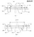
- Figure 1 describes a conventional ATE interface signal module 100.
- An ATE interface electromagnetic signal 106 is transmitted through signal module 100 along spring pin 104.
- the electromagnetic signal propagates in the region 108 surrounding the surfaces of the spring pins, (multiple spring pins not shown) and encounters dielectric caps 102 at the module ends along with any dielectric shims 116 within the signal module.
- reflections 112 of the electromagnetic signal occur when the electromagnetic signal encounters the boundary interface between the media surrounding spring pin 104 and the dielectric caps 102.
- a typical ATE interface signal module may employ dielectric caps whose dielectric constant is greater than air. This creates a characteristic impedance mismatch, resulting in the electromagnetic reflections 112.
- the magnitude of the electromagnetic reflections increase as the dielectric constant of the dielectric caps increase. Additionally, the forward transmission coefficient suffers loss causing decreased transmission through the signal module.
- the final electromagnetic signal 110 transmitted through the conventional signal module may include transmission loss and crosstalk from adjacent spring pins.
- Efforts to reduce electromagnetic reflections in an ATE interface signal module have attempted to compensate for the capacitive effect of the dielectric cap. For example, the spring pin diameter in a portion of the dielectric cap has been adjusted in an effort to achieve an impedance match.
- the present invention produces an electromagnetic impedance match by implementing the condition where the plane of the incident TM (transverse magnetic) field of the electromagnetic wave propagating along the axis of the signal module is parallel with the surface of the dielectric boundary.
- An angle of the dielectric boundary surface is thus determined based on the electromagnetic field produced as a result of the signal flowing through the signal module.
- this is desirably accomplished by creating a bevel angle at the boundary of the media between the spring pins and the dielectric caps.
- An exemplary embodiment of the present invention comprises a signal module including a conductor and a low loss dielectric.
- dielectrics 202 and 204 and conductor 208 are shown in Figure 2 .
- Figure 2 illustrates a signal module 200 according to an exemplary embodiment of the present invention.
- the conductor may pass through dielectrics 202 and 204 in signal module 200. Additional dielectrics such as dielectric 216 may also be positioned along the length of conductor to provide further support to the conductor.
- An electromagnetic signal 210 may be sent into one end of the exemplary signal module.
- the electromagnetic signal is an electromagnetic wave that propagates along the axis of conductor 208.
- the electromagnetic signal desirably passes through dielectrics 202 and 204 without producing reflections in region 212 between dielectrics 202 and 204.
- Signal 214 that is transmitted out of signal module 200 desirably has no transmission loss from passing through dielectrics 202 and 204.
- ATE interface signals typically have a bandwidth in the GHz region.
- Signal module 200 desirably operates in the frequency region between DC and at least 30 GHz and higher.
- Exemplary signal module 200 may operate at a substantially higher bandwidth or within a more limited bandwidth.
- the exemplary signal module is not limited to ATE interface signals and may be used for other applications, such as connectors that include internal dielectric inserts intended to mechanically support electrical conductors within the connector but also obstruct the propagation of electromagnetic signals that pass through them.
- Signal module 200 shown here presents dielectric 204 as having one angle 206. This is being shown for illustrative purposes only.
- dielectrics 202 and 204 are at the same bevel angle 206.
- dielectrics 202 and 204 show only one surface with bevel angle 206, in the exemplary embodiment, all surfaces are desirably at a specific bevel angle. Additionally, dielectrics 202 and 204 only show one segment of the specific bevel angle.
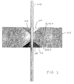
- the bevel angle is a conical shaped countersink 302 of Figure 3 , which is convenient for fabrication.
- a dielectric 204 has a first surface 204a and a second surface 204b.
- a conductor 208 passes through first surface 204a having a countersink 302.
- Countersink 302 is desirably at angle 206 relative to a central axis along the length of conductor 208.
- Conductor 208 further passes through second surface 204b, also having a countersink 302. It is desirable that surfaces 204a and 204b each have countersinks 302, both at bevel angle 206.
- Exemplary conductor 208 may be included in a pseudo-coaxial transmission line comprised of a plurality of conductors. Pseudo-coaxial transmission lines are commonly known by one skilled in the art.
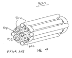
- Figure 4 illustrates a known in the art pseudo-coaxial transmission line 400 composed of five parallel spring pins 402 and 404.
- center pin 404 carries the electromagnetic signal and the other four spring pins 402, which are arranged to surround center pin 404 are electrically grounded.
- This and other potentially useful configurations are shown, for example, in Reference Data for Radio Engineers, 4th Edition. New York: International Telephone & Circuit Corp., 1957 .
- the present invention is not limited to spring pin arrangement 400 or to a pseudo-coaxial transmission line.
- the transmission lines used in exemplary signal module 200 typically seek to achieve a characteristic impedance of 50 Ohms. This characteristic impedance matches the impedance of typical coaxial cables, printed circuit boards microstrip transmission lines or other electrical devices that may be attached to the exemplary signal module. Signal module 200 may be designed to achieve other characteristic impedance values.
- the characteristic impedance of a transmission line may be governed by the geometric arrangement of the spring pins, the diameter of the spring pins, the spacing distance between spring pins, and the dielectric constant of the media between the pins.
- Other media may include other dielectric medium with a low loss tangent and stable, frequency independent dielectric constant.
- Exemplary signal module 200 with conductor 208 may operate with a planar electric field vector from an electromagnetic signal, such as but not limited to TM01 or TE11 wave modes for a circular geometric arrangement of conductors forming a transmission line, or TE10 or TM11 wave modes for a rectangular geometry of conductors forming a transmission line.
- the exemplary signal module also desirably operates with electromagnetic signals having distorted electric field vector.
- a distorted TM field vector may occur where conductor 208 is a pseudo-coaxial transmission line or in other configurations.
- Dielectrics 202 and 204 may include dielectric material having a dielectric constant between 1 to 5 over a frequency range of DC to at least 30 GHz and higher.
- the frequency range for which the dielectric constant is desirably between 1 to 5 may be substantially higher.
- the dielectric constant is desirably constant over a preferred bandwidth.
- the dielectric constant value and frequency range desirably depends upon the application of the exemplary signal module. The desired dielectric constant value and frequency range may vary with the type of input signal without affecting the scope of the present invention.
- the dielectric material also desirably includes the property of a loss tangent less than 0.1 over the frequency range of DC to at least 30 GHz and higher.
- the frequency range for which the loss tangent is desirably less than 0.1 may be substantially higher.
- the loss tangent required depends upon the application of the signal module. ATE interface signals may require lower loss tangents than other applications.
- Common dielectric materials used in exemplary signal module 200 may include polytetrafluoroethylene, FR4, Ultem ® 1000, Rexolite ® , polyethylene, polyvinylchloride and air. Other materials may be used provided they have a low loss tangent (for example less than 0.1) and dielectric constant suitable for the application requirements. All dielectric materials, including those listed here, exhibit some loss, albeit a small loss that may be considered negligible.
- an electromagnetic impedance match at the boundary of two media with differing dielectric constants may be achieved if the plane of the incident TM field of the electromagnetic wave propagating along the axis of the signal module is parallel with the surface of the dielectric boundary, and the boundary is at a specific bevel angle. This bevel angle is determined from the angle where the electromagnetic reflection approaches a zero value.
- the surface of the dielectric of the exemplary embodiment is desirably smooth and contains a straight line parallel to the TM field plane of incidence where they intersect and where the electromagnetic wave propagates along a linear axis.
- the surface of the dielectric desirably conforms to an isosurface of the TM field for other electromagnetic wave conditions.
- the angle where electromagnetic reflections approach a minimum value may be calculated using the principles of a Brewster angle.
- the Brewster angle is common in the art of optical and quasi-optical systems.
- ⁇ B the Brewster angle
- ⁇ 1 and ⁇ 2 are the dielectric constants of regions 1 and 2 respectively
- ⁇ T is the refractive angle of region 2.
- the bevel angle is dependent upon the dielectric constant of the dielectric, the dielectric constant of the media surrounding the conductor, and the angle of the TM field vector from the electromagnetic signal propagating along the conductor.
- the bevel angle is desirably further modified to account for the distortion. Therefore, the bevel angle is not a classic Brewster angle, but an angle that accounts for electric field distortion caused by the type of conductor, such as a pseudo-coaxial transmission line.
- the criteria for an electromagnetic impedance match are those as defined in equation (2) but the implementation desirably requires modification to account for electric field distortion in order to accommodate those criteria.
- the improvement in transmission is broadband and not dependent upon the signal frequency.
- Frequency dependence is limited by the frequency dependence of the dielectric material permittivity.
- frequency dependence is also limited by the electromagnetic mode cut-off frequency well known to transmission line designers.
- the present invention may be extended to a signal module with multiple conductors, as shown in Figure 5.
- Figure 5 shows a cross-sectioned portion of one end of a dielectric cap 500. Multiple conductors 502, 504 and 506 extend through the dielectric cap 500 and out of a signal module according to an exemplary embodiment of the present invention.
- Figure 5 shows bevel angles 508, 510 and 512 corresponding to conductors 502, 504, and 506.
- the bevel angles illustrated here more accurately depict the implementation of bevel angles on the dielectric surface.
- the bevel angles are desirably countersinks on the dielectric.
- the multiple countersinks are desirably adjacent to or intersect each other.
- the conductors illustrated in the embodiment of Figure 5 may each represent an individual conductor of, for example, a five-wire a pseudo-coaxial transmission line such as illustrated in Figure 4 or other transmission lines, or signal carrying connector.
- the exemplary embodiment is not limited to a device of three conductors.
- the exemplary signal module may contain any number of conductors in a planar or other suitable arrangement. The conductors may be spaced apart and in such an arrangement to provide an appropriate characteristic impedance match to its connecting devices.
- the bevel angle applied to the surface of the dielectric for each respective conductor causes the electromagnetic reflection along each conductor to approach a minimum value.
- the even mode is defined as simultaneous signals propagating in a parallel direction, in contrast to an odd mode where simultaneous signals are propagating in an anti-parallel direction.
- the exemplary embodiment may include any combination of even and odd mode propagation conditions simultaneously.
- a first electromagnetic signal may propagate into the end of conductor 502 while a second electromagnetic signal may propagate out of the end of conductor 504.
- the second electromagnetic signal thus propagates in a direction opposite the first electromagnetic signal.
- Respective bevel angles 508, 510 and 512 may each be designed for the specific electromagnetic signal and may be of a different angle to remove reflections for the particular electromagnetic signal. This allows manufacture of a signal module suited to a particular application. The resulting signal module will have a minimum of channel cross-talk and a maximum of respective signal transmission.
- Figures 6 illustrates an exemplary pseudo-coaxial transmission line 600 with five dielectrics 606 spaced apart from each other along pseudo-coaxial transmission line 600.
- Each dielectric 606 has a bevel angle countersink (not shown) on both sides of dielectric 606 determined as described above.
- Pseudo-coaxial transmission line 600 has five spring pins 602 and 604.
- Center spring pin 604 carries the electromagnetic signal and the other four spring pins 602, which are arranged to surround center pin 604 are electrically grounded.
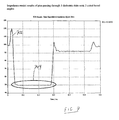
- Impedance model simulation results 702 illustrate the impedance in ohms of an electromagnetic signal propagating through exemplary pseudo-coaxial transmission line 600 versus time in ns.
- the impedance is about 50 ohms, as illustrated by region 704.
- Exemplary embodiment 600 demonstrates that although the electromagnetic signal encounters 10 boundary condition changes (two for each dielectric 606) the bevel angle countersinks on each dielectric significantly reduce an impedance mismatch, thus maintaining the impedance at about 50 ohms.
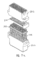
- a retainer cap 802 of dielectric material covers and supports spring pins 816.
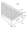
- a section of retainer cap 802 is further illustrated in Figure 8b .
- Retainer cap 802 has a top portion 804 and a side portion 812.
- a first surface of top portion 804 includes a plurality of bevel angle countersinks 806.
- a plurality of apertures 808 extends between bevel angle countersinks 806 and a second surface of top portion 804.
- a second surface 810 of top portion 804 is a flat surface and does not have bevel angle countersinks due to machining limitations.
- a bevel angle shim 814 is of dielectric material having a first surface that is flat and a second surface with bevel angle countersinks. Bevel angle shim further includes apertures corresponding to the apertures in the retainer cap 802 and the countersinks of bevel angle shim 814. The first surface of bevel angle shim 814 is disposed adjacent to the second surface 810 of top portion 804 of retainer cap 802. The combination of dielectric retainer cap 802 and bevel angle shim 812 function as one retainer with both surfaces having bevel angle countersinks.
- An assembly shim 818 is disposed between side portion 812 of a first retainer cap 802 and a side portion 812 of a second retainer cap 802.
- Assembly shim 818 has apertures corresponding to the apertures in first retainer cap 802.
- Assembly shim 818 is desirably of dielectric material with bevel angle countersinks machined on both sides corresponding to the apertures.
- Assembly shim 818 may provide support to spring pins 816.
- a second retainer cap 802 and bevel angle shim 814 as described above are coupled together to function as one retainer with both surfaces having bevel angle countersinks.
- Both second retainer cap 802 and second bevel angle shim 814 further include apertures that correspond to the apertures in first retainer cap 802.
- a plurality of spring pins 816 extend and are supported through the apertures between top portion 804 of first retainer cap 802, first bevel angle shim 814, assembly shim 818, a second bevel angle shim 814 and top portion 804 of a second retainer cap 802. Side portions 812 of first and second retainer caps 802 enclose spring pins 816 within exemplary ATE signal interface module 800.
- ATE signal Interface module 800 all dielectric boundaries are thus provided with countersink bevel angles designed as described above according to an exemplary method of the present invention. Exemplary module 800 thus does not suffer from impedance mismatch.
- the invention is defined by the following claims.
Abstract
Description
- The present invention relates to electronic interfacing and more particularly, an apparatus and method for substantially reducing electromagnetic reflections in a signal interface module.
- In the manufacture of integrated circuits (ICs) and other electronic devices, testing with automatic test equipment (ATE) is performed at one or more stages of the overall process. IC testing systems typically include a test head and a probe card. Packaged part testing systems typically include a test head and a device under test (DUT) board. The probe card or DUT board includes a pattern of contacts for electrically probing or connecting to portions of an integrated circuit. The test head is configured to drive various contacts of the probe card or DUT board to carry out particular test procedures within the IC. In the course of a test procedure, the test head receives output signals from the IC via the contacts of the probe card or DUT board. The output signals are indicative of electrical characteristics of the IC under test. The probe card or DUT board and the test head are uniquely configured for a particular IC and, in some cases, a particular test procedure. Accordingly, the probe card or DUT board and/or the test head must be changed for different ICs and test procedures.
- The test head is electrically coupled to the probe card or DUT board with an interface apparatus. The interface apparatus may be, for example, a zero insertion force socket or a "pogo" unit. A pogo unit engages the test head, or some intermediate coupling structure associated with the test head, and the probe card or DUT board. The pogo unit includes an array of spring-loaded contact pins referred to as Pogo Pins®. The spring pins act as signal and ground conductors, and are arranged to electrically couple contacts on the probe card or DUT board to corresponding contacts on the test head. The spring force of the spring pins helps to maintain uniformity of electrical contact between the various contacts of the probe card or DUT board and the test head. When the test head and probe card or DUT board are engaged with the pogo unit exerting pressure against the spring pins, the spring pins respond with a spring force that enhances coupling pressure. The resilience of the pins generally ensures adequate coupling pressure despite planar deformation of the test head or the probe card or DUT board during a test procedure.
- In many applications, the conductors are required to carry signals having very high frequency components, from 100's of MHz to 10 GHz In the near future and to 10's of GHz in the more distant future. Accordingly, the transmission line characteristic impedance of the signal path between the probe card or DUT board and the test head is of prime interest. For optimal signal transfer between the test electronics and the device being tested, the characteristic impedance of all elements in the signal path should be closely matched. Usually, it is desired that all signal paths have the same impedance, for example 28, 50, or 75 Ohms, though it may be required that several different values of characteristic impedance be provided in the same interface.
- ATE interface signal modules typically employ dielectric materials to structurally support electrical transmission lines. These dielectric materials provide an electrically insulating boundary between adjacent transmission line elements, but also cause discontinuities in the characteristic impedance along the path of the transmission line. Discontinuities in characteristic impedance along a transmission line can cause undesirable effects that include increased reflection coefficients levels, consequent decreased transmission coefficient levels, both of which are frequency dependent, that causes unleveled channel performance detrimental to the signal integrity of the signal module and its ability to perform ATE signal characterization. In many applications it is thus desirable to remove the reflections of electromagnetic fields as they propagate through the impedance discontinuities caused by the differing dielectric constants.
WO 02/07265 A
PatentUS-3,437,960 describes a dielectric bead structure for coaxial connectors. PatentUS-3,310,358 describes a conical lens focusing means for TM0n Modes. - The invention is defined by the subject-matter of the independent claims. The dependent claims are directed to advantageous embodiments.
- Advantageously, it is provided a signal module for electrically interfacing with an electronic device. The signal module includes a dielectric and a conductor extending through a surface of the dielectric. The surface of the dielectric is located away from perpendicular relative to an axis of the conductor and is located based on an electromagnetic field produced as a result of a signal flowing through the conductor.
- Advantageously, it is provided a method of transmitting an electromagnetic signal. The method includes the step of providing a signal module. The signal module includes a dielectric and a conductor extending through a surface of the dielectric. The surface of the dielectric is away from perpendicular relative to an axis of the conductor and the surface is based on an electromagnetic field produced as a result of a signal flowing through the conductor. The method further includes the steps of providing the electromagnetic signal to one end of the conductor in the signal module and transmitting the signal through the conductor.
- Advantageously, it is provided a signal connector. The signal connector includes a dielectric having a countersink provided on each of a first surface and a second surface opposite the first surface. The signal connector also includes a conductor that extends through the countersink of the first surface of the dielectric and the countersink of the second surface of the dielectric. The dielectric provides mechanical support to the conductor. The countersinks are provided at a bevel angle relative to an axis of the conductor and located based on an electromagnetic field produced as a result of a signal flowing through the conductor.
- Advantageously, it is provided a signal module. The signal module includes a plurality of spring pins and a first and second retainer cap. Each retainer cap is of dielectric materials. Each retainer cap includes a top portion having a plurality of countersinks provided in each of a first surface and a second surface opposite the first surface and a plurality of bores extending between the plurality of countersinks provided in the first surface and the second surface. Each retainer cap also includes a side portion that is coupled to the top portion. The side portion encloses the plurality of spring pins. The plurality of spring pins are disposed in the plurality of bores, respectively. The countersinks are provided at a bevel angle relative to an axis of the conductor and located based on an electromagnetic field produced as a result of a plurality of signals flowing through the plurality of spring pins, respectively.
- The invention is best understood from the following detailed description when read in connection with the accompanying drawing. It is emphasized that, according to common practice, the various features of the drawing are not to scale. On the contrary, the dimensions of the various features are arbitrarily expanded or reduced for clarity. Included in the drawing are the following figures:
-
Figure 1 is a side view of a conventional signal module showing electromagnetic signal propagation and reflection through the conventional signal module; -
Figure 2 is a side view of an exemplary signal module in accordance with an exemplary embodiment of the present invention showing electromagnetic signal propagation through the exemplary signal module; -
Figure 3 is a side view of an exemplary dielectric boundary in accordance with an exemplary embodiment of the present invention showing countersinks in the dielectric boundary in a vicinity of a conductor; -
Figure 4 is a perspective view of a conventional pseudo-coaxial transmission line showing an arrangement of conductors through an end terminal of the pseudo-coaxial transmission line; -
Figure 5 is a side view section of an exemplary signal module of the present invention showing an arrangement of conductors through a dielectric having bevel angles for each respective conductor; -
Figure 6 is a perspective view of an exemplary pseudo-coaxial transmission line in accordance with an exemplary embodiment of the present invention showing five dielectrics with bevel angle countersinks arranged along the pseudo-coaxial transmission line; -
Figure 7 is a simulation result of the impedance of an electromagnetic signal propagating through the exemplary pseudo-coaxial transmission line in accordance with an exemplary embodiment of the present invention; -
Figure 8a is a perspective view of an exemplary ATE interface signal module in accordance with an exemplary embodiment of the present invention; and -
Figure 8b is a section view of a retainer cap within an exemplary ATE interface in accordance with an exemplary embodiment of the present invention. -
Figure 1 describes a conventional ATEinterface signal module 100. An ATE interfaceelectromagnetic signal 106 is transmitted throughsignal module 100 alongspring pin 104. The electromagnetic signal propagates in theregion 108 surrounding the surfaces of the spring pins, (multiple spring pins not shown) and encountersdielectric caps 102 at the module ends along with anydielectric shims 116 within the signal module. - In the conventional ATE interface signal module,
reflections 112 of the electromagnetic signal occur when the electromagnetic signal encounters the boundary interface between the media surroundingspring pin 104 and thedielectric caps 102. - The media surrounding the spring pins is typically air. A typical ATE interface signal module may employ dielectric caps whose dielectric constant is greater than air. This creates a characteristic impedance mismatch, resulting in the
electromagnetic reflections 112. - The magnitude of the electromagnetic reflections increase as the dielectric constant of the dielectric caps increase. Additionally, the forward transmission coefficient suffers loss causing decreased transmission through the signal module.
- Multiple spring pins (not shown in
Figure 1 ) passing throughdielectric caps 102 may each haveelectromagnetic reflections 112. The resulting reflections may produce undesirable crosstalk between adjacent spring pins. Thus, the finalelectromagnetic signal 110 transmitted through the conventional signal module may include transmission loss and crosstalk from adjacent spring pins. - Attempts have been made to match the impedance of the dielectric with that of the media surrounding the spring pins. Attempts to fabricate dielectric caps using materials of very low dielectric constant, for example, Cuming Microwave Corporation RH-10 material, have revealed that the mechanical tensile strength of those materials is not sufficient to rigidly constrain the spring pins.
- Efforts to reduce electromagnetic reflections in an ATE interface signal module have attempted to compensate for the capacitive effect of the dielectric cap. For example, the spring pin diameter in a portion of the dielectric cap has been adjusted in an effort to achieve an impedance match.
- In "calculation of an Optimum Transmission Line Taper," IEEE Microwave Theory & Techniques, November 1972, pages 734-739, the diameter of the plunger was gradually changed to compensate for capacitive effect of the dielectric cap. A computer simulation model constructed that computed the required length of the tapered transmission line resulted in requiring an unacceptably long transmission line not capable of fitting within the constrained dimensions of a reasonable ATE signal module.
- The present invention produces an electromagnetic impedance match by implementing the condition where the plane of the incident TM (transverse magnetic) field of the electromagnetic wave propagating along the axis of the signal module is parallel with the surface of the dielectric boundary. An angle of the dielectric boundary surface is thus determined based on the electromagnetic field produced as a result of the signal flowing through the signal module. In an ATE signal module, this is desirably accomplished by creating a bevel angle at the boundary of the media between the spring pins and the dielectric caps. By providing the appropriate bevel angle, there are essentially zero reflections between dielectric boundaries.
- An exemplary embodiment of the present invention comprises a signal module including a conductor and a low loss dielectric. In an exemplary embodiment,
dielectrics conductor 208 are shown inFigure 2 . -
Figure 2 illustrates asignal module 200 according to an exemplary embodiment of the present invention. The conductor may pass throughdielectrics signal module 200. Additional dielectrics such asdielectric 216 may also be positioned along the length of conductor to provide further support to the conductor. - An
electromagnetic signal 210 may be sent into one end of the exemplary signal module. The electromagnetic signal is an electromagnetic wave that propagates along the axis ofconductor 208. The electromagnetic signal desirably passes throughdielectrics region 212 betweendielectrics Signal 214 that is transmitted out ofsignal module 200 desirably has no transmission loss from passing throughdielectrics - ATE interface signals typically have a bandwidth in the GHz region.
Signal module 200 desirably operates in the frequency region between DC and at least 30 GHz and higher.Exemplary signal module 200 may operate at a substantially higher bandwidth or within a more limited bandwidth. The exemplary signal module is not limited to ATE interface signals and may be used for other applications, such as connectors that include internal dielectric inserts intended to mechanically support electrical conductors within the connector but also obstruct the propagation of electromagnetic signals that pass through them. -
Signal module 200 shown here presents dielectric 204 as having oneangle 206. This is being shown for illustrative purposes only. InFigure 2 ,dielectrics same bevel angle 206. Althoughdielectrics bevel angle 206, in the exemplary embodiment, all surfaces are desirably at a specific bevel angle. Additionally,dielectrics countersink 302 ofFigure 3 , which is convenient for fabrication. - As illustrated in
Figure 3 , a dielectric 204 has a first surface 204a and a second surface 204b. Aconductor 208 passes through first surface 204a having acountersink 302.Countersink 302 is desirably atangle 206 relative to a central axis along the length ofconductor 208.Conductor 208 further passes through second surface 204b, also having acountersink 302. It is desirable that surfaces 204a and 204b each have countersinks 302, both atbevel angle 206. -
Exemplary conductor 208 may be included in a pseudo-coaxial transmission line comprised of a plurality of conductors. Pseudo-coaxial transmission lines are commonly known by one skilled in the art. -
Figure 4 illustrates a known in the artpseudo-coaxial transmission line 400 composed of five parallel spring pins 402 and 404. In this example,center pin 404 carries the electromagnetic signal and the other fourspring pins 402, which are arranged to surroundcenter pin 404 are electrically grounded. This is only one arrangement of a pseudo-coaxial transmission line. This and other potentially useful configurations are shown, for example, in Reference Data for Radio Engineers, 4th Edition. New York: International Telephone & Telegraph Corp., 1957. The present invention is not limited tospring pin arrangement 400 or to a pseudo-coaxial transmission line. - The transmission lines used in
exemplary signal module 200 typically seek to achieve a characteristic impedance of 50 Ohms. This characteristic impedance matches the impedance of typical coaxial cables, printed circuit boards microstrip transmission lines or other electrical devices that may be attached to the exemplary signal module.Signal module 200 may be designed to achieve other characteristic impedance values. - The characteristic impedance of a transmission line may be governed by the geometric arrangement of the spring pins, the diameter of the spring pins, the spacing distance between spring pins, and the dielectric constant of the media between the pins. The media surround the spring pins, and hence
conductor 208 inregion 212, is typically air. Other media may include other dielectric medium with a low loss tangent and stable, frequency independent dielectric constant. -
Exemplary signal module 200 withconductor 208 may operate with a planar electric field vector from an electromagnetic signal, such as but not limited to TM01 or TE11 wave modes for a circular geometric arrangement of conductors forming a transmission line, or TE10 or TM11 wave modes for a rectangular geometry of conductors forming a transmission line. The exemplary signal module also desirably operates with electromagnetic signals having distorted electric field vector. A distorted TM field vector may occur whereconductor 208 is a pseudo-coaxial transmission line or in other configurations. -
Dielectrics - In addition to the dielectric constant constraints of
dielectrics - Common dielectric materials used in
exemplary signal module 200 may include polytetrafluoroethylene, FR4, Ultem® 1000, Rexolite®, polyethylene, polyvinylchloride and air. Other materials may be used provided they have a low loss tangent (for example less than 0.1) and dielectric constant suitable for the application requirements. All dielectric materials, including those listed here, exhibit some loss, albeit a small loss that may be considered negligible. - According to the present invention, an electromagnetic impedance match at the boundary of two media with differing dielectric constants may be achieved if the plane of the incident TM field of the electromagnetic wave propagating along the axis of the signal module is parallel with the surface of the dielectric boundary, and the boundary is at a specific bevel angle. This bevel angle is determined from the angle where the electromagnetic reflection approaches a zero value.
- The surface of the dielectric of the exemplary embodiment is desirably smooth and contains a straight line parallel to the TM field plane of incidence where they intersect and where the electromagnetic wave propagates along a linear axis. The surface of the dielectric desirably conforms to an isosurface of the TM field for other electromagnetic wave conditions.
- The angle where electromagnetic reflections approach a minimum value may be calculated using the principles of a Brewster angle. The Brewster angle is common in the art of optical and quasi-optical systems.
- For parallel polarization, the Brewster angle, θB, exists where there is an angle of incidence upon the dielectric at which the TM Fresnel reflection vanishes for nonmagnetic and lossless materials. The initial condition is defined by Snell's Law as shown in equation (1).

where ε1 and ε2 are the dielectric constants ofregions region 2. - From simple geometry, it can be shown that θT = 90° - θ8, it follows that


known as Brewster's Law and typically expressed as below
- For the exemplary embodiment of the signal module, the bevel angle is dependent upon the dielectric constant of the dielectric, the dielectric constant of the media surrounding the conductor, and the angle of the TM field vector from the electromagnetic signal propagating along the conductor.
- The Brewster angle computed by
equation 2 above assumes the dielectric media are lossless, i.e. exhibit zero electrical conductivity and are nonmagnetic. The Brewster angle loses its meaning if the dielectric material inregion 2 is l ossy since it will exhibit a complex valued dielectric constant. The Brewster angle may be modified by specifying the real and imaginary parts of the complex dielectric. The electromagnetic reflection can approach a minimum value if we re-stateequation 2 as
- This approach is known as the Zenneck Surface Wave when the incident medium is lossless, such as air, which is the medium ε1.
- For determining appropriate bevel angles and surfaces for particular applications and configurations of real materials regardless of the loss tangent of the dielectric and the distortion of the TM vector resulting from various configurations, commercially available modeling and simulation tools such as Finite Difference Time Domain solvers with three-dimensional capabilities can be used.
- To accommodate distorted electric fields, the bevel angle is desirably further modified to account for the distortion. Therefore, the bevel angle is not a classic Brewster angle, but an angle that accounts for electric field distortion caused by the type of conductor, such as a pseudo-coaxial transmission line. The criteria for an electromagnetic impedance match are those as defined in equation (2) but the implementation desirably requires modification to account for electric field distortion in order to accommodate those criteria.
- At the specific bevel angle value, electromagnetic reflections approach zero. The transmission out of the signal module subsequently improves to a high value as it is commonly known from the conservation of energy.
- The improvement in transmission is broadband and not dependent upon the signal frequency. Frequency dependence is limited by the frequency dependence of the dielectric material permittivity. For an exemplary embodiment where the conductor is a transmission line, frequency dependence is also limited by the electromagnetic mode cut-off frequency well known to transmission line designers.
- The present invention may be extended to a signal module with multiple conductors, as shown in
Figure 5. Figure 5 shows a cross-sectioned portion of one end of adielectric cap 500.Multiple conductors dielectric cap 500 and out of a signal module according to an exemplary embodiment of the present invention. -
Figure 5 shows bevel angles 508, 510 and 512 corresponding toconductors - The conductors illustrated in the embodiment of
Figure 5 may each represent an individual conductor of, for example, a five-wire a pseudo-coaxial transmission line such as illustrated inFigure 4 or other transmission lines, or signal carrying connector. The exemplary embodiment is not limited to a device of three conductors. The exemplary signal module may contain any number of conductors in a planar or other suitable arrangement. The conductors may be spaced apart and in such an arrangement to provide an appropriate characteristic impedance match to its connecting devices. - The bevel angle applied to the surface of the dielectric for each respective conductor causes the electromagnetic reflection along each conductor to approach a minimum value. The adjacent channel crosstalk, both even mode and odd mode, decreases since there is no reflection mechanism to contribute to the crosstalk.
- In bidirectional signaling, multiple conductor transmission lines carrying any multiplicity of signals simultaneously, the even mode is defined as simultaneous signals propagating in a parallel direction, in contrast to an odd mode where simultaneous signals are propagating in an anti-parallel direction. The exemplary embodiment may include any combination of even and odd mode propagation conditions simultaneously.
- It is understood that the invention is not limited to multiple electromagnetic signals propagating in the same direction along multiple conductors, respectively. For example, a first electromagnetic signal may propagate into the end of
conductor 502 while a second electromagnetic signal may propagate out of the end ofconductor 504. The second electromagnetic signal thus propagates in a direction opposite the first electromagnetic signal. - Different electromagnetic signals with differing electric field vectors may propagate through
conductors - The invention will next be illustrated by reference to a number of examples. The examples are included to more clearly demonstrate the overall nature of the invention. These examples are exemplary, not restrictive of the invention.
-
Figures 6 illustrates an exemplary pseudo-coaxial transmission line 600 with fivedielectrics 606 spaced apart from each other along pseudo-coaxial transmission line 600. Each dielectric 606 has a bevel angle countersink (not shown) on both sides of dielectric 606 determined as described above. Pseudo-coaxial transmission line 600 has fivespring pins 602 and 604. Center spring pin 604 carries the electromagnetic signal and the other fourspring pins 602, which are arranged to surround center pin 604 are electrically grounded. - Referring now to
Figure 7 , results of an impedance model simulation with respect to exemplary pseudo-coaxial transmission line 600 is now described. Impedance model simulation results 702 illustrate the impedance in ohms of an electromagnetic signal propagating through exemplary pseudo-coaxial transmission line 600 versus time in ns. When the electromagnetic signal propagates through exemplary pseudo-coaxial transmission line 600, the impedance is about 50 ohms, as illustrated byregion 704. Exemplary embodiment 600 demonstrates that although the electromagnetic signal encounters 10 boundary condition changes (two for each dielectric 606) the bevel angle countersinks on each dielectric significantly reduce an impedance mismatch, thus maintaining the impedance at about 50 ohms. - Referring now to
Figure 8a , an exemplary ATE signal interface module 800 with multiple spring pins 816 is now described. Aretainer cap 802 of dielectric material covers and supports spring pins 816. - A section of
retainer cap 802 is further illustrated inFigure 8b .Retainer cap 802 has atop portion 804 and aside portion 812. A first surface oftop portion 804 includes a plurality of bevel angle countersinks 806. A plurality ofapertures 808 extends between bevel angle countersinks 806 and a second surface oftop portion 804. Asecond surface 810 oftop portion 804 is a flat surface and does not have bevel angle countersinks due to machining limitations. - A
bevel angle shim 814 is of dielectric material having a first surface that is flat and a second surface with bevel angle countersinks. Bevel angle shim further includes apertures corresponding to the apertures in theretainer cap 802 and the countersinks ofbevel angle shim 814. The first surface ofbevel angle shim 814 is disposed adjacent to thesecond surface 810 oftop portion 804 ofretainer cap 802. The combination ofdielectric retainer cap 802 andbevel angle shim 812 function as one retainer with both surfaces having bevel angle countersinks. - An
assembly shim 818 is disposed betweenside portion 812 of afirst retainer cap 802 and aside portion 812 of asecond retainer cap 802.Assembly shim 818 has apertures corresponding to the apertures infirst retainer cap 802.Assembly shim 818 is desirably of dielectric material with bevel angle countersinks machined on both sides corresponding to the apertures.Assembly shim 818 may provide support to spring pins 816. - A
second retainer cap 802 andbevel angle shim 814 as described above are coupled together to function as one retainer with both surfaces having bevel angle countersinks. Bothsecond retainer cap 802 and secondbevel angle shim 814 further include apertures that correspond to the apertures infirst retainer cap 802. - A plurality of spring pins 816 extend and are supported through the apertures between
top portion 804 offirst retainer cap 802, firstbevel angle shim 814,assembly shim 818, a secondbevel angle shim 814 andtop portion 804 of asecond retainer cap 802.Side portions 812 of first and second retainer caps 802 enclosespring pins 816 within exemplary ATE signal interface module 800. - In exemplary ATE signal Interface module 800, all dielectric boundaries are thus provided with countersink bevel angles designed as described above according to an exemplary method of the present invention. Exemplary module 800 thus does not suffer from impedance mismatch. The invention is defined by the following claims.
Claims (43)
- A signal module (200; 800) for electrically interfacing with an electronic device, said signal module (200; 800) comprising:a plurality of conductors (208; 404; 502, 504, 506; 604) configured to carry respective electromagnetic signals (210); andat least one solid support (202, 204; 500; 802) of dielectric material having a surface (204a, 204b) perpendicular to axes of said conductors (208; 404; 502, 504, 506; 604), said solid support (202, 204; 500; 802) having depressions (302; 806) symmetric with respect to said axes, said depressions (302; 806) each having a base on said surface (204a, 204b) and an apex within said solid support (202, 204; 500; 802), said depression (302; 806) each provided at a bevel angle (206; 508, 510, 512) relative to said axes, said bevel angle being chosen so that there are essentially zero reflections between the dielectric boundaries,wherein said conductors (208; 404; 502, 504, 506; 604) extend through said solid support (202, 204; 500; 802) via each apex of said depressions (302; 806), each of said
conductors (208; 404; 502, 504, 506; 604) being spaced apart from each other of said conductors (208; 404; 502, 504, 506; 604). - The signal module (200; 800) according to claim 1, wherein said solid support (202, 204; 500; 802) is one of a plurality of solid supports (202, 204; 500; 802), said plurality of solid supports (202; 204; 500; 802) spaced apart from each other along the axis of said conductor (208; 204; 502, 504, 506; 604).
- The signal module (200; 800) according to claim 1, wherein said dielectric material includes a loss tangent less than 0.1 over a DC to 30 GHz frequency range.
- The signal module (200; 800) according to claim 1, wherein said dielectric material includes a dielectric constant between 1 and 5 that remains constant over a DC to 30 GHz frequency range.
- The signal module (200; 800) according to claim 1, wherein said conductor (208; 404; 502, 504, 506; 604) is one of at least copper, brass, brass alloys, aluminum, silver, graphite and gold.
- The signal module (200; 800) according to claim 1, wherein said conductor (208; 404; 502, 504, 506; 604) is surrounded by a medium with low loss tangent and stable dielectric constant.
- The signal module (200; 800) according to claim 1, wherein said conductor (208; 404; 502, 504, 506; 604) is a transmission line (400; 600).
- The signal module (200; 800) according to claim 7, wherein said transmission line (400; 600) is a pseudo-coaxial transmission line (400; 600).
- The signal module (200; 800) according to claim 1, wherein said conductor (208; 404; 502, 504, 506; 604) is one of a plurality of conductors (208; 402, 404; 502, 504, 506; 602, 604; 816), where said conductors (208; 402, 404; 502, 504, 506; 602, 604; 816) are spaced apart from each other and extend through said solid support (202, 204; 500; 802).
- The signal module (200; 800) according to claim 1, wherein said conductor (208; 404; 502, 504, 506; 604) is configured to carry said electromagnetic signal (210) and said electromagnetic signal (210) is an electromagnetic wave (210) that propagates along the axis of said conductor (208; 404; 502, 504, 506; 604).
- The signal module (200; 800) according to claim 1, wherein said bevel angle (206, 508) is located at a boundary between said medium surrounding the conductor (208; 404; 502, 504, 506; 604) and said solid support (202, 204; 500; 802).
- The signal module (200; 800) according to claim 11, wherein said bevel angle (206; 508, 510, 512) provides an electromagnetic impedance match at said boundary between said conductor (208; 404; 502, 504, 506; 604) and said solid support (202, 204; 500; 802).
- The signal module (200; 800) according to claim 11, wherein said depression (302; 806) includes a countersink (302; 806) having said bevel angle (206; 508, 510, 512) that is provided in said solid support (202, 204; 500; 802), said countersink (302; 806) located at said boundary between said conductor (208; 404; 502, 504, 506; 604) and said solid support (202, 204; 500; 802).
- The signal module (200; 800) according to claim 1, wherein said bevel angle (206; 508, 510, 512) provides a characteristic impedance that substantially matches a characteristic impedance of said electrical device coupled to said signal module (200; 800).
- The signal module (200; 800) according to claim 1, said surface of said solid support (202, 204; 500; 802) is one of multiple surfaces, wherein the multiple surfaces have respective bevel angles (206; 508, 510, 512).
- The signal module (200; 800) according to claim 1, wherein said bevel angle (206; 508, 510, 512) is one of a plurality of bevel angles (206; 508, 510, 512) for a respective plurality of conductors (208; 402, 404; 502, 504, 506; 602, 604; 816), wherein said bevel angle (206; 508, 510, 512) for at least one of said respective plurality of conductors (208; 402, 404; 502, 504, 506; 602, 604; 816), is different from the bevel angle (206; 508, 510, 512) of the other respective conductors (208; 402, 404; 502, 504, 506; 602, 604; 816).
- The signal module (200; 800) according to claim 16, wherein said electromagnetic signal (210) is one of a plurality of electromagnetic signals, said plurality of conductors (208; 402, 404; 502, 504, 506; 602, 604; 816) configured to transmit said plurality of electromagnetic signals through said respective plurality of conductors (208; 402, 404; 502, 504, 506; 602, 604; 816), wherein at least one of said electromagnetic signals transmitted through said respective plurality of conductors (208; 402, 404; 502, 504, 506; 602, 604; 816) is different from the electromagnetic signals transmitted through the other respective conductors (208; 402,404;502,504,506;602,604;816).
- The signal module (200; 800) according to claim 17, wherein at least one of said electromagnetic signals transmitted through said respective plurality of conductors (208; 402, 404; 502, 504, 506; 602, 604; 816) propagates in a direction opposite from the electromagnetic signals transmitted through the other respective conductors (208; 402, 404; 502, 504, 506; 602, 604; 816).
- The signal module (200; 800) according to claim 1, wherein said bevel angle (206, 508, 510, 512) is one of a plurality of bevel angles (206; 508, 510, 512) for a respective plurality of conductors (208; 402, 404; 502, 504, 506; 602, 604; 816), said plurality of bevel angles (206; 508, 510, 512) provides a substantial reduction of cross-talk between said respective plurality of electromagnetic signals.
- The signal module (200; 800) according to claim 1, wherein:the solid support (202, 204; 500; 802) comprises a depression (302; 806) provided in each of a first surface (204a) and a second surface (204b) opposite said first surface (204a), said first surface (204a) and said second surface (204b) being perpendicular to an axis of said conductor (208; 404; 502, 504, 506; 604), each depression (302; 806) being symmetric with respect to said axis, each depression having an apex within said solid support (202, 204; 500; 802) and a base on said first surface (204a) and said second surface (204b), respectively, each depression (302; 806) provided at a bevel angle (206; 508, 510, 512) relative to said axis; andwherein said conductor (208; 404; 502, 504, 506; 604) is disposed through said solid support (202, 204; 500; 802) and extends through said apex of said depression of said first surface and said apex of said depression (302; 806) of said second surface (204b), respectively.
- The signal module (200; 800) according to claim 20, wherein said solid support (202, 204; 500; 802) is one of a plurality of solid supports (202, 204; 500; 802), said plurality of solid supports (202, 204; 500; 802) spaced apart from each other along said axis of said conductor (208; 404; 502, 504, 506; 604).
- The signal module (200; 800) according to claim 20, wherein said conductor (208; 404; 502, 504, 506; 604) is one of a plurality of conductors (208; 402, 404; 502, 504, 506; 604), where said conductors (208; 402, 404; 502, 504, 506; 602, 604; 816) are spaced part from each other and extend through one of a plurality of depressions (302; 806) provided on said first surface (204a) of said solid support (202, 204; 500; 802) and one of a plurality of depressions (302; 806) provided on said second surface (204b) of said solid support (202, 204; 500; 802), respectively.
- The signal module (200; 800) according to claim 20, wherein said conductor (208; 404; 502, 504, 506; 604) is a transmission line (400; 600).
- The signal module (200; 800) according to claim 23, wherein said transmission line (400; 600) is a pseudo-coaxial transmission line (400; 600), said pseudo-coaxial transmission line (400; 600) comprising a signal-carrying conductor (404; 504; 604) that is configured to carry said electromagnetic signal (210) and a plurality of conductors (402; 502, 506; 602) surrounding said signal-carrying conductor (404; 504; 604), each one of said plurality of conductors (402; 502; 506; 602) being electrically grounded.
- The signal module (200; 800) according to claim 20, wherein said bevel angle (206; 508, 510, 512) provides an electromagnetic impedance match at respective boundaries between said medium surrounding the conductor (208; 404; 502, 504, 506; 604) and said solid support (202, 204; 500; 802).
- The signal module (200; 800) according to claim 20, wherein said bevel angle (206; 508, 510, 512) provides a characteristic impedance that substantially matches a characteristic impedance of an electrical device coupled to said signal module (200; 800).
- The signal module (200; 800), according to claim 1, further comprising:a plurality of conductors (208; 402, 404; 502, 504, 506; 602, 604; 816), wherein at least one of the plurality of conductors (208; 402, 404; 502, 504, 506; 602, 604; 816) is configured to carry an electromagnetic signal (210); andat least one support of dielectric material (202, 204; 500; 802), said at least one support (202, 204; 500; 802) having plurality of depressions (302; 806) provided in each of a first surface (204a) and a second surface (204b) opposite said first surface (204a), wherein said plurality of conductors (208; 402, 404; 502, 504, 506; 602, 604; 816) are disposed through said at least one support (202, 204; 500; 802) and extend through said plurality of depressions (302; 806) of said first surface (204a) and said plurality of depressions (302; 806) of said second surface (204b) of said support (202, 204; 500; 802), respectively, andeach of said depressions (302; 806) are provided at a bevel angle (206; 508, 510, 512) relative to an axis of a respective one of said plurality of conductors (208; 402, 404; 502, 504, 506; 602, 604; 816).
- The signal module (200; 800) according to claim 27, wherein said bevel angle (206; 508, 510, 512) provides an electromagnetic impedance match at a respective boundary between a medium surrounding said plurality of conductors (208; 402, 404; 502, 504, 506; 602, 604; 816) and said at least one support (202, 204; 500; 802).
- The signal module (200; 800) according to claim 27, wherein said bevel angle (206; 508, 510, 512) provides a characteristic impedance that substantially matches a characteristic impedance of an electrical device coupled to said signal module (200; 800).
- The signal module (200; 800) according to claim 27, said at least one support (202, 204; 500; 802) including a first retainer cap (802) and second retainer cap (802).
- The signal module (200; 800) according to claim 30, further comprising a shim (814) of dielectric material disposed between said first and said second retainer caps (802), said shim (814) comprising:a plurality of shim depressions provided in each of a first surface and a second surface opposite said first surface of said shim (814), said plurality of shim depressions corresponding to said plurality of depressions of said first and second retainer caps (802),wherein said plurality of conductors (208; 402, 404; 502, 504, 506; 602, 604; 816) are disposed through said shim and extend through said plurality of shim (814) depressions of said first surface of said shim (814) and said plurality of shim depressions of said second surface of said shim (814), respectively.
- The signal module (200; 800) according to claim 1, wherein said at least one solid support (202, 204; 500; 802) includes a further surface having depressions provided at a further bevel angle relative to said axes.
- The signal module (200; 800) according to claim 1, wherein said at least one solid support (202, 204; 500; 802) includes a further support with a further surface having depressions provided at a further bevel angle relative to said axes.
- A method of transmitting an electromagnetic signal (210), the method comprising:a) providing a signal module according to any one of claims 1 to 33;b) providing said electromagnetic signal (210) to one end of said conductors (208; 404; 502, 504, 506; 604) in said signal module (200; 800); andc) transmitting said electromagnetic signal (210) through the conductors (208; 404; 502, 504, 506; 604).
- The method according to claim 34, wherein said solid support (202, 204; 500; 802) is one of a plurality of solid supports (202, 204; 500; 802), said plurality of solid support (202, 204; 500; 802) spaced apart from each other along said axis of said conductor (208; 404; 502, 504, 506; 604), so that in stepc c) said electromagnetic signal (210) is transmitted through said plurality of solid supports (202, 204; 500; 802).
- The method according to claim 34, wherein said conductor (208; 404; 502, 504, 506; 604) is one of a plurality of conductors (208; 402, 404; 502, 504, 506; 602, 604; 816), where said conductors (208; 402, 404; 502, 504, 506; 602, 604; 816) are spaced apart from each other and extend through said solid support (202, 204; 500; 802), said electromagnetic signal (210) is one of a plurality of electromagnetic signals transmitted through said conductors (208; 404; 502, 504, 506; 604), respectively.
- The method according to claim 36, wherein at least one of said electromagnetic signals transmitted through said conductors (208; 402, 404; 502, 504, 506; 602, 604; 816) propagates in a direction opposite from the electromagnetic signals transmitted through the other respective conductors (208; 404; 502, 504, 506; 604).
- The method according to claim 34, wherein the step b) includes providing the electromagnetic signal (210) comprising said electromagnetic wave that propagates along said axis of the conductor (208; 404; 502, 504, 506; 604).
- The method according to claim 34, said surface of said solid support (202, 204; 500; 802) is one of multiple surfaces, wherein the multiple surfaces, wherein the multiple surfaces have respective bevel angles (206; 508, 510, 512), so that in step c) said electromagnetic signal (210) is transmitted through said solid support (202, 204; 500; 802).
- The method according to claim 34, said bevel angle (206; 508, 510, 512) provides an electromagnetic impedance match for said electromagnetic signal (210) transmitted at a boundary between said solid support (202, 204; 500; 802) and said medium surrounding the conductor (208; 404; 502, 504, 506; 604).
- The method according to claim 34, said bevel angle (206; 508, 510, 512) provides a characteristic impedance such that the characteristic impedance of said electromagnetic signal (210) transmitted through the conductor (208; 404; 502, 504, 506; 604) substantially matches a characteristic impedance of an electrical device coupled to a second end of said conductor (208; 404; 502, 504, 506; 604).
- The method according to claim 34, wherein the electromagnetic signal (210) is one of a plurality of electromagnetic signals transmitted through said conductors (208; 404; 502, 504, 506; 604) respectively.
- The method according to claim 34, said bevel angle (206; 508, 510, 512) is one of a plurality of bevel angles (206; 508, 510, 512) for a respective plurality of conductors (208; 402, 404; 502, 504, 506; 602, 604; 816), said electromagnetic signal (210) is one of a plurality of electromagnetic signals transmitted through said conductors (208; 404; 502, 504, 506; 604) respectively, wherein said bevel angle (206; 508, 510, 512) provides a substantial reduction of cross-talk between said respective plurality of electromagnetic signals.
Applications Claiming Priority (2)
| Application Number | Priority Date | Filing Date | Title |
|---|---|---|---|
| US63564204P | 2004-12-13 | 2004-12-13 | |
| PCT/US2005/044730 WO2006065669A1 (en) | 2004-12-13 | 2005-12-09 | Signal module with reduced reflections |
Publications (2)
| Publication Number | Publication Date |
|---|---|
| EP1825282A1 EP1825282A1 (en) | 2007-08-29 |
| EP1825282B1 true EP1825282B1 (en) | 2009-12-09 |
Family
ID=36168623
Family Applications (1)
| Application Number | Title | Priority Date | Filing Date |
|---|---|---|---|
| EP05853612A Active EP1825282B1 (en) | 2004-12-13 | 2005-12-09 | Signal module with reduced reflections |
Country Status (9)
| Country | Link |
|---|---|
| US (1) | US7834718B2 (en) |
| EP (1) | EP1825282B1 (en) |
| JP (1) | JP5185625B2 (en) |
| KR (1) | KR101225519B1 (en) |
| CN (1) | CN100593726C (en) |
| AT (1) | ATE451623T1 (en) |
| DE (1) | DE602005018255D1 (en) |
| HK (1) | HK1111465A1 (en) |
| WO (1) | WO2006065669A1 (en) |
Families Citing this family (61)
| Publication number | Priority date | Publication date | Assignee | Title |
|---|---|---|---|---|
| US9910144B2 (en) | 2013-03-07 | 2018-03-06 | Cpg Technologies, Llc | Excitation and use of guided surface wave modes on lossy media |
| US9912031B2 (en) | 2013-03-07 | 2018-03-06 | Cpg Technologies, Llc | Excitation and use of guided surface wave modes on lossy media |
| US9941566B2 (en) | 2014-09-10 | 2018-04-10 | Cpg Technologies, Llc | Excitation and use of guided surface wave modes on lossy media |
| US9882397B2 (en) | 2014-09-11 | 2018-01-30 | Cpg Technologies, Llc | Guided surface wave transmission of multiple frequencies in a lossy media |
| US9960470B2 (en) * | 2014-09-11 | 2018-05-01 | Cpg Technologies, Llc | Site preparation for guided surface wave transmission in a lossy media |
| US9887557B2 (en) | 2014-09-11 | 2018-02-06 | Cpg Technologies, Llc | Hierarchical power distribution |
| US9887587B2 (en) | 2014-09-11 | 2018-02-06 | Cpg Technologies, Llc | Variable frequency receivers for guided surface wave transmissions |
| US10027116B2 (en) | 2014-09-11 | 2018-07-17 | Cpg Technologies, Llc | Adaptation of polyphase waveguide probes |
| US10033198B2 (en) | 2014-09-11 | 2018-07-24 | Cpg Technologies, Llc | Frequency division multiplexing for wireless power providers |
| US9887556B2 (en) | 2014-09-11 | 2018-02-06 | Cpg Technologies, Llc | Chemically enhanced isolated capacitance |
| US9893402B2 (en) | 2014-09-11 | 2018-02-13 | Cpg Technologies, Llc | Superposition of guided surface waves on lossy media |
| US10074993B2 (en) | 2014-09-11 | 2018-09-11 | Cpg Technologies, Llc | Simultaneous transmission and reception of guided surface waves |
| US10498393B2 (en) | 2014-09-11 | 2019-12-03 | Cpg Technologies, Llc | Guided surface wave powered sensing devices |
| US10101444B2 (en) | 2014-09-11 | 2018-10-16 | Cpg Technologies, Llc | Remote surface sensing using guided surface wave modes on lossy media |
| US9859707B2 (en) | 2014-09-11 | 2018-01-02 | Cpg Technologies, Llc | Simultaneous multifrequency receive circuits |
| US10001553B2 (en) | 2014-09-11 | 2018-06-19 | Cpg Technologies, Llc | Geolocation with guided surface waves |
| US10079573B2 (en) | 2014-09-11 | 2018-09-18 | Cpg Technologies, Llc | Embedding data on a power signal |
| US10175203B2 (en) | 2014-09-11 | 2019-01-08 | Cpg Technologies, Llc | Subsurface sensing using guided surface wave modes on lossy media |
| US9859658B2 (en) * | 2015-05-14 | 2018-01-02 | Te Connectivity Corporation | Electrical connector having resonance controlled ground conductors |
| US10193595B2 (en) | 2015-06-02 | 2019-01-29 | Cpg Technologies, Llc | Excitation and use of guided surface waves |
| US9923385B2 (en) | 2015-06-02 | 2018-03-20 | Cpg Technologies, Llc | Excitation and use of guided surface waves |
| KR20180050726A (en) | 2015-09-08 | 2018-05-15 | 씨피지 테크놀로지스, 엘엘씨. | Long distance transmission of marine power |
| US9997040B2 (en) | 2015-09-08 | 2018-06-12 | Cpg Technologies, Llc | Global emergency and disaster transmission |
| US9857402B2 (en) | 2015-09-08 | 2018-01-02 | CPG Technologies, L.L.C. | Measuring and reporting power received from guided surface waves |
| US9887585B2 (en) | 2015-09-08 | 2018-02-06 | Cpg Technologies, Llc | Changing guided surface wave transmissions to follow load conditions |
| US9921256B2 (en) | 2015-09-08 | 2018-03-20 | Cpg Technologies, Llc | Field strength monitoring for optimal performance |
| US10063095B2 (en) | 2015-09-09 | 2018-08-28 | CPG Technologies, Inc. | Deterring theft in wireless power systems |
| US9973037B1 (en) | 2015-09-09 | 2018-05-15 | Cpg Technologies, Llc | Object identification system and method |
| EA201890665A1 (en) * | 2015-09-09 | 2018-09-28 | Сипиджи Текнолоджиз, Элэлси. | PROBES OF THE DIRECTED SURFACE WAVEGUIDE |
| US9916485B1 (en) | 2015-09-09 | 2018-03-13 | Cpg Technologies, Llc | Method of managing objects using an electromagnetic guided surface waves over a terrestrial medium |
| US9887558B2 (en) | 2015-09-09 | 2018-02-06 | Cpg Technologies, Llc | Wired and wireless power distribution coexistence |
| US9927477B1 (en) | 2015-09-09 | 2018-03-27 | Cpg Technologies, Llc | Object identification system and method |
| US10205326B2 (en) | 2015-09-09 | 2019-02-12 | Cpg Technologies, Llc | Adaptation of energy consumption node for guided surface wave reception |
| WO2017044281A1 (en) * | 2015-09-09 | 2017-03-16 | Cpg Technologies, Llc | Guided surface waveguide probes |
| MA42077B1 (en) | 2015-09-09 | 2019-10-31 | Cpg Technologies Llc | Electrical internal medical devices with guided surface waves |
| US10031208B2 (en) | 2015-09-09 | 2018-07-24 | Cpg Technologies, Llc | Object identification system and method |
| US9882436B2 (en) | 2015-09-09 | 2018-01-30 | Cpg Technologies, Llc | Return coupled wireless power transmission |
| EP3345276B1 (en) | 2015-09-09 | 2019-10-09 | CPG Technologies, LLC | Load shedding in a guided surface wave power delivery system |
| US10027131B2 (en) | 2015-09-09 | 2018-07-17 | CPG Technologies, Inc. | Classification of transmission |
| US10033197B2 (en) | 2015-09-09 | 2018-07-24 | Cpg Technologies, Llc | Object identification system and method |
| US9496921B1 (en) | 2015-09-09 | 2016-11-15 | Cpg Technologies | Hybrid guided surface wave communication |
| US10103452B2 (en) | 2015-09-10 | 2018-10-16 | Cpg Technologies, Llc | Hybrid phased array transmission |
| US10498006B2 (en) | 2015-09-10 | 2019-12-03 | Cpg Technologies, Llc | Guided surface wave transmissions that illuminate defined regions |
| KR20180051573A (en) * | 2015-09-10 | 2018-05-16 | 씨피지 테크놀로지스, 엘엘씨. | Global time synchronization using surface wave |
| US10312747B2 (en) | 2015-09-10 | 2019-06-04 | Cpg Technologies, Llc | Authentication to enable/disable guided surface wave receive equipment |
| US10559893B1 (en) * | 2015-09-10 | 2020-02-11 | Cpg Technologies, Llc | Pulse protection circuits to deter theft |
| US10396566B2 (en) | 2015-09-10 | 2019-08-27 | Cpg Technologies, Llc | Geolocation using guided surface waves |
| US10408916B2 (en) * | 2015-09-10 | 2019-09-10 | Cpg Technologies, Llc | Geolocation using guided surface waves |
| US10324163B2 (en) | 2015-09-10 | 2019-06-18 | Cpg Technologies, Llc | Geolocation using guided surface waves |
| US10408915B2 (en) | 2015-09-10 | 2019-09-10 | Cpg Technologies, Llc | Geolocation using guided surface waves |
| CN108351399A (en) | 2015-09-10 | 2018-07-31 | Cpg技术有限责任公司 | Use the geo-location of lead schedule surface wave |
| US10601099B2 (en) | 2015-09-10 | 2020-03-24 | Cpg Technologies, Llc | Mobile guided surface waveguide probes and receivers |
| US10193229B2 (en) | 2015-09-10 | 2019-01-29 | Cpg Technologies, Llc | Magnetic coils having cores with high magnetic permeability |
| US9893403B2 (en) | 2015-09-11 | 2018-02-13 | Cpg Technologies, Llc | Enhanced guided surface waveguide probe |
| EA201890711A1 (en) | 2015-09-11 | 2018-09-28 | Сипиджи Текнолоджиз, Элэлси. | GLOBAL MULTIPLICATION OF ELECTRICAL POWER |
| US20200190192A1 (en) | 2017-03-07 | 2020-06-18 | Sutro Biopharma, Inc. | Pd-1/tim-3 bi-specific antibodies, compositions thereof, and methods of making and using the same |
| US10559866B2 (en) | 2017-03-07 | 2020-02-11 | Cpg Technologies, Inc | Measuring operational parameters at the guided surface waveguide probe |
| US10581492B1 (en) | 2017-03-07 | 2020-03-03 | Cpg Technologies, Llc | Heat management around a phase delay coil in a probe |
| US10630111B2 (en) | 2017-03-07 | 2020-04-21 | Cpg Technologies, Llc | Adjustment of guided surface waveguide probe operation |
| US10559867B2 (en) | 2017-03-07 | 2020-02-11 | Cpg Technologies, Llc | Minimizing atmospheric discharge within a guided surface waveguide probe |
| US10560147B1 (en) | 2017-03-07 | 2020-02-11 | Cpg Technologies, Llc | Guided surface waveguide probe control system |
Family Cites Families (9)
| Publication number | Priority date | Publication date | Assignee | Title |
|---|---|---|---|---|
| US3310358A (en) * | 1963-05-01 | 1967-03-21 | Bell Telephone Labor Inc | Conical lens focusing means for tmon modes |
| US3437960A (en) | 1966-03-30 | 1969-04-08 | Amp Inc | Dielectric bead structure for coaxial connectors |
| DE2020173C3 (en) | 1970-04-24 | 1981-01-08 | Spinner-Gmbh Elektrotechnische Fabrik, 8000 Muenchen | Insulating support arrangement in coaxial lines |
| US3750086A (en) * | 1972-01-03 | 1973-07-31 | Gen Tel Co Calif | Rapid connector |
| EP0465845A3 (en) * | 1990-06-15 | 1992-06-10 | Asea Brown Boveri Ag | Microwave window |
| US5269702A (en) * | 1992-10-23 | 1993-12-14 | Helmut Bacher | Coaxial support structure |
| US5961355A (en) * | 1997-12-17 | 1999-10-05 | Berg Technology, Inc. | High density interstitial connector system |
| US6652326B2 (en) * | 2000-07-13 | 2003-11-25 | Rika Electronics International, Inc. | Contact apparatus particularly useful with test equipment |
| US6844738B2 (en) * | 2001-12-10 | 2005-01-18 | Intel Corporation | Coaxial radio frequency adapter and method |
-
2005
- 2005-12-09 DE DE602005018255T patent/DE602005018255D1/en active Active
- 2005-12-09 US US11/721,492 patent/US7834718B2/en not_active Expired - Fee Related
- 2005-12-09 WO PCT/US2005/044730 patent/WO2006065669A1/en active Application Filing
- 2005-12-09 JP JP2007546783A patent/JP5185625B2/en not_active Expired - Fee Related
- 2005-12-09 EP EP05853612A patent/EP1825282B1/en active Active
- 2005-12-09 AT AT05853612T patent/ATE451623T1/en not_active IP Right Cessation
- 2005-12-09 CN CN200580042838A patent/CN100593726C/en not_active Expired - Fee Related
- 2005-12-09 KR KR1020077015842A patent/KR101225519B1/en not_active IP Right Cessation
-
2008
- 2008-01-24 HK HK08100887.8A patent/HK1111465A1/en not_active IP Right Cessation
Also Published As
| Publication number | Publication date |
|---|---|
| HK1111465A1 (en) | 2008-08-08 |
| KR101225519B1 (en) | 2013-01-24 |
| JP5185625B2 (en) | 2013-04-17 |
| DE602005018255D1 (en) | 2010-01-21 |
| US20080273201A1 (en) | 2008-11-06 |
| KR20070090243A (en) | 2007-09-05 |
| JP2008523411A (en) | 2008-07-03 |
| CN100593726C (en) | 2010-03-10 |
| US7834718B2 (en) | 2010-11-16 |
| ATE451623T1 (en) | 2009-12-15 |
| EP1825282A1 (en) | 2007-08-29 |
| WO2006065669A1 (en) | 2006-06-22 |
| CN101080643A (en) | 2007-11-28 |
Similar Documents
| Publication | Publication Date | Title |
|---|---|---|
| EP1825282B1 (en) | Signal module with reduced reflections | |
| US7492146B2 (en) | Impedance controlled via structure | |
| US6501278B1 (en) | Test structure apparatus and method | |
| US6856131B2 (en) | Magnetic sensor, side-opened TEM cell, and apparatus using such magnetic sensor and side-opened TEM cell | |
| TWI479732B (en) | Spring loaded microwave interconnector | |
| US6939175B2 (en) | Coaxial cable for overvoltage protection | |
| US20090120668A1 (en) | Cabled Signaling System and Components Thereof | |
| US4980636A (en) | Universal nondestructive MM-wave integrated circuit test fixture | |
| US7013452B2 (en) | Method and apparatus for intra-layer transitions and connector launch in multilayer circuit boards | |
| KR20170073323A (en) | Printed circuit board having high-speed signal connector | |
| TWI414791B (en) | Test arrangement, pogo-pin and method for testing a device under test | |
| US20030042912A1 (en) | Hybrid conductor-board for multi-conductor routing | |
| US7423497B2 (en) | Device for coupling suspended stripline and NRD guides | |
| US20220236302A1 (en) | Hybrid shielding sockets with impedance tuning for integrated circuit device test tooling | |
| US11624764B1 (en) | Flange mount coaxial connector system | |
| US20030062914A1 (en) | Surface mating compliant contact assembly with fixed signal path length | |
| CN220368259U (en) | Interface board and device for testing channel physical layer C-PHY signal | |
| US6842084B2 (en) | Transition from a coaxial transmission line to a printed circuit transmission line | |
| US7049903B2 (en) | Transition from a coaxial transmission line to a printed circuit transmission line | |
| Rosas et al. | Development of a 1.85 mm coaxial blind mating interconnect for ATE applications | |
| WO2023284314A1 (en) | Test structural member and test system | |
| Siebert | High frequency cable connector for twisted pair cables | |
| Berg | Multi-GHz elastomeric connectors for complex hybrids and chip carriers | |
| KR19980087354A (en) | Circuit board |
Legal Events
| Date | Code | Title | Description |
|---|---|---|---|
| PUAI | Public reference made under article 153(3) epc to a published international application that has entered the european phase |
Free format text: ORIGINAL CODE: 0009012 |
|
| 17P | Request for examination filed |
Effective date: 20070530 |
|
| AK | Designated contracting states |
Kind code of ref document: A1 Designated state(s): AT BE BG CH CY CZ DE DK EE ES FI FR GB GR HU IE IS IT LI LT LU LV MC NL PL PT RO SE SI SK TR |
|
| 17Q | First examination report despatched |
Effective date: 20080111 |
|
| DAX | Request for extension of the european patent (deleted) | ||
| REG | Reference to a national code |
Ref country code: HK Ref legal event code: DE Ref document number: 1111465 Country of ref document: HK |
|
| GRAP | Despatch of communication of intention to grant a patent |
Free format text: ORIGINAL CODE: EPIDOSNIGR1 |
|
| GRAS | Grant fee paid |
Free format text: ORIGINAL CODE: EPIDOSNIGR3 |
|
| GRAA | (expected) grant |
Free format text: ORIGINAL CODE: 0009210 |
|
| AK | Designated contracting states |
Kind code of ref document: B1 Designated state(s): AT BE BG CH CY CZ DE DK EE ES FI FR GB GR HU IE IS IT LI LT LU LV MC NL PL PT RO SE SI SK TR |
|
| REG | Reference to a national code |
Ref country code: GB Ref legal event code: FG4D |
|
| REG | Reference to a national code |
Ref country code: CH Ref legal event code: EP |
|
| REG | Reference to a national code |
Ref country code: IE Ref legal event code: FG4D |
|
| REF | Corresponds to: |
Ref document number: 602005018255 Country of ref document: DE Date of ref document: 20100121 Kind code of ref document: P |
|
| REG | Reference to a national code |
Ref country code: SE Ref legal event code: TRGR |
|
| REG | Reference to a national code |
Ref country code: NL Ref legal event code: T3 |
|
| REG | Reference to a national code |
Ref country code: HK Ref legal event code: GR Ref document number: 1111465 Country of ref document: HK |
|
| PG25 | Lapsed in a contracting state [announced via postgrant information from national office to epo] |
Ref country code: LT Free format text: LAPSE BECAUSE OF FAILURE TO SUBMIT A TRANSLATION OF THE DESCRIPTION OR TO PAY THE FEE WITHIN THE PRESCRIBED TIME-LIMIT Effective date: 20091209 Ref country code: FI Free format text: LAPSE BECAUSE OF FAILURE TO SUBMIT A TRANSLATION OF THE DESCRIPTION OR TO PAY THE FEE WITHIN THE PRESCRIBED TIME-LIMIT Effective date: 20091209 |
|
| LTIE | Lt: invalidation of european patent or patent extension |
Effective date: 20091209 |
|
| PG25 | Lapsed in a contracting state [announced via postgrant information from national office to epo] |
Ref country code: SI Free format text: LAPSE BECAUSE OF FAILURE TO SUBMIT A TRANSLATION OF THE DESCRIPTION OR TO PAY THE FEE WITHIN THE PRESCRIBED TIME-LIMIT Effective date: 20091209 Ref country code: LV Free format text: LAPSE BECAUSE OF FAILURE TO SUBMIT A TRANSLATION OF THE DESCRIPTION OR TO PAY THE FEE WITHIN THE PRESCRIBED TIME-LIMIT Effective date: 20091209 Ref country code: PL Free format text: LAPSE BECAUSE OF FAILURE TO SUBMIT A TRANSLATION OF THE DESCRIPTION OR TO PAY THE FEE WITHIN THE PRESCRIBED TIME-LIMIT Effective date: 20091209 |
|
| PG25 | Lapsed in a contracting state [announced via postgrant information from national office to epo] |
Ref country code: AT Free format text: LAPSE BECAUSE OF FAILURE TO SUBMIT A TRANSLATION OF THE DESCRIPTION OR TO PAY THE FEE WITHIN THE PRESCRIBED TIME-LIMIT Effective date: 20091209 |
|
| PG25 | Lapsed in a contracting state [announced via postgrant information from national office to epo] |
Ref country code: EE Free format text: LAPSE BECAUSE OF FAILURE TO SUBMIT A TRANSLATION OF THE DESCRIPTION OR TO PAY THE FEE WITHIN THE PRESCRIBED TIME-LIMIT Effective date: 20091209 Ref country code: ES Free format text: LAPSE BECAUSE OF FAILURE TO SUBMIT A TRANSLATION OF THE DESCRIPTION OR TO PAY THE FEE WITHIN THE PRESCRIBED TIME-LIMIT Effective date: 20100320 Ref country code: MC Free format text: LAPSE BECAUSE OF NON-PAYMENT OF DUE FEES Effective date: 20100701 Ref country code: RO Free format text: LAPSE BECAUSE OF FAILURE TO SUBMIT A TRANSLATION OF THE DESCRIPTION OR TO PAY THE FEE WITHIN THE PRESCRIBED TIME-LIMIT Effective date: 20091209 Ref country code: PT Free format text: LAPSE BECAUSE OF FAILURE TO SUBMIT A TRANSLATION OF THE DESCRIPTION OR TO PAY THE FEE WITHIN THE PRESCRIBED TIME-LIMIT Effective date: 20100409 Ref country code: BG Free format text: LAPSE BECAUSE OF FAILURE TO SUBMIT A TRANSLATION OF THE DESCRIPTION OR TO PAY THE FEE WITHIN THE PRESCRIBED TIME-LIMIT Effective date: 20100309 Ref country code: IS Free format text: LAPSE BECAUSE OF FAILURE TO SUBMIT A TRANSLATION OF THE DESCRIPTION OR TO PAY THE FEE WITHIN THE PRESCRIBED TIME-LIMIT Effective date: 20100409 |
|
| REG | Reference to a national code |
Ref country code: CH Ref legal event code: PL |
|
| PG25 | Lapsed in a contracting state [announced via postgrant information from national office to epo] |
Ref country code: BE Free format text: LAPSE BECAUSE OF FAILURE TO SUBMIT A TRANSLATION OF THE DESCRIPTION OR TO PAY THE FEE WITHIN THE PRESCRIBED TIME-LIMIT Effective date: 20091209 Ref country code: CZ Free format text: LAPSE BECAUSE OF FAILURE TO SUBMIT A TRANSLATION OF THE DESCRIPTION OR TO PAY THE FEE WITHIN THE PRESCRIBED TIME-LIMIT Effective date: 20091209 Ref country code: SK Free format text: LAPSE BECAUSE OF FAILURE TO SUBMIT A TRANSLATION OF THE DESCRIPTION OR TO PAY THE FEE WITHIN THE PRESCRIBED TIME-LIMIT Effective date: 20091209 |
|
| PLBE | No opposition filed within time limit |
Free format text: ORIGINAL CODE: 0009261 |
|
| STAA | Information on the status of an ep patent application or granted ep patent |
Free format text: STATUS: NO OPPOSITION FILED WITHIN TIME LIMIT |
|
| PG25 | Lapsed in a contracting state [announced via postgrant information from national office to epo] |
Ref country code: LI Free format text: LAPSE BECAUSE OF NON-PAYMENT OF DUE FEES Effective date: 20091231 Ref country code: CH Free format text: LAPSE BECAUSE OF NON-PAYMENT OF DUE FEES Effective date: 20091231 Ref country code: CY Free format text: LAPSE BECAUSE OF FAILURE TO SUBMIT A TRANSLATION OF THE DESCRIPTION OR TO PAY THE FEE WITHIN THE PRESCRIBED TIME-LIMIT Effective date: 20091209 Ref country code: GR Free format text: LAPSE BECAUSE OF FAILURE TO SUBMIT A TRANSLATION OF THE DESCRIPTION OR TO PAY THE FEE WITHIN THE PRESCRIBED TIME-LIMIT Effective date: 20100310 Ref country code: IE Free format text: LAPSE BECAUSE OF NON-PAYMENT OF DUE FEES Effective date: 20091209 |
|
| 26N | No opposition filed |
Effective date: 20100910 |
|
| PG25 | Lapsed in a contracting state [announced via postgrant information from national office to epo] |
Ref country code: DK Free format text: LAPSE BECAUSE OF FAILURE TO SUBMIT A TRANSLATION OF THE DESCRIPTION OR TO PAY THE FEE WITHIN THE PRESCRIBED TIME-LIMIT Effective date: 20091209 |
|
| PG25 | Lapsed in a contracting state [announced via postgrant information from national office to epo] |
Ref country code: IT Free format text: LAPSE BECAUSE OF NON-PAYMENT OF DUE FEES Effective date: 20091209 |
|
| PG25 | Lapsed in a contracting state [announced via postgrant information from national office to epo] |
Ref country code: LU Free format text: LAPSE BECAUSE OF NON-PAYMENT OF DUE FEES Effective date: 20091209 |
|
| PG25 | Lapsed in a contracting state [announced via postgrant information from national office to epo] |
Ref country code: HU Free format text: LAPSE BECAUSE OF FAILURE TO SUBMIT A TRANSLATION OF THE DESCRIPTION OR TO PAY THE FEE WITHIN THE PRESCRIBED TIME-LIMIT Effective date: 20100610 |
|
| PGRI | Patent reinstated in contracting state [announced from national office to epo] |
Ref country code: IT Effective date: 20110616 |
|
| PG25 | Lapsed in a contracting state [announced via postgrant information from national office to epo] |
Ref country code: TR Free format text: LAPSE BECAUSE OF FAILURE TO SUBMIT A TRANSLATION OF THE DESCRIPTION OR TO PAY THE FEE WITHIN THE PRESCRIBED TIME-LIMIT Effective date: 20091209 |
|
| PGFP | Annual fee paid to national office [announced via postgrant information from national office to epo] |
Ref country code: SE Payment date: 20131206 Year of fee payment: 9 |
|
| PGFP | Annual fee paid to national office [announced via postgrant information from national office to epo] |
Ref country code: GB Payment date: 20141124 Year of fee payment: 10 |
|
| PGFP | Annual fee paid to national office [announced via postgrant information from national office to epo] |
Ref country code: NL Payment date: 20141209 Year of fee payment: 10 |
|
| PG25 | Lapsed in a contracting state [announced via postgrant information from national office to epo] |
Ref country code: SE Free format text: LAPSE BECAUSE OF NON-PAYMENT OF DUE FEES Effective date: 20141210 |
|
| REG | Reference to a national code |
Ref country code: SE Ref legal event code: EUG |
|
| REG | Reference to a national code |
Ref country code: FR Ref legal event code: PLFP Year of fee payment: 11 |
|
| GBPC | Gb: european patent ceased through non-payment of renewal fee |
Effective date: 20151209 |
|
| REG | Reference to a national code |
Ref country code: NL Ref legal event code: MM Effective date: 20160101 |
|
| PG25 | Lapsed in a contracting state [announced via postgrant information from national office to epo] |
Ref country code: GB Free format text: LAPSE BECAUSE OF NON-PAYMENT OF DUE FEES Effective date: 20151209 Ref country code: NL Free format text: LAPSE BECAUSE OF NON-PAYMENT OF DUE FEES Effective date: 20160101 |
|
| REG | Reference to a national code |
Ref country code: FR Ref legal event code: PLFP Year of fee payment: 12 |
|
| REG | Reference to a national code |
Ref country code: FR Ref legal event code: PLFP Year of fee payment: 13 |
|
| PGFP | Annual fee paid to national office [announced via postgrant information from national office to epo] |
Ref country code: FR Payment date: 20171113 Year of fee payment: 13 |
|
| PGFP | Annual fee paid to national office [announced via postgrant information from national office to epo] |
Ref country code: IT Payment date: 20171221 Year of fee payment: 13 |
|
| PG25 | Lapsed in a contracting state [announced via postgrant information from national office to epo] |
Ref country code: IT Free format text: LAPSE BECAUSE OF NON-PAYMENT OF DUE FEES Effective date: 20181209 Ref country code: FR Free format text: LAPSE BECAUSE OF NON-PAYMENT OF DUE FEES Effective date: 20181231 |
|
| PGFP | Annual fee paid to national office [announced via postgrant information from national office to epo] |
Ref country code: DE Payment date: 20191126 Year of fee payment: 15 |
|
| REG | Reference to a national code |
Ref country code: DE Ref legal event code: R119 Ref document number: 602005018255 Country of ref document: DE |
|
| PG25 | Lapsed in a contracting state [announced via postgrant information from national office to epo] |
Ref country code: DE Free format text: LAPSE BECAUSE OF NON-PAYMENT OF DUE FEES Effective date: 20210701 |