EP3056343B1 - Fluorharzbasismaterial, leiterplatte und schaltungsmodul - Google Patents
Fluorharzbasismaterial, leiterplatte und schaltungsmodul Download PDFInfo
- Publication number
- EP3056343B1 EP3056343B1 EP14852835.9A EP14852835A EP3056343B1 EP 3056343 B1 EP3056343 B1 EP 3056343B1 EP 14852835 A EP14852835 A EP 14852835A EP 3056343 B1 EP3056343 B1 EP 3056343B1
- Authority
- EP
- European Patent Office
- Prior art keywords
- fluororesin
- base material
- modified layer
- group
- layer
- Prior art date
- Legal status (The legal status is an assumption and is not a legal conclusion. Google has not performed a legal analysis and makes no representation as to the accuracy of the status listed.)
- Active
Links
- 239000000463 material Substances 0.000 title claims description 431
- 238000000576 coating method Methods 0.000 claims description 52
- 239000011248 coating agent Substances 0.000 claims description 51
- 229920001721 polyimide Polymers 0.000 claims description 51
- 239000004642 Polyimide Substances 0.000 claims description 50
- 238000005530 etching Methods 0.000 claims description 44
- 239000000853 adhesive Substances 0.000 claims description 43
- 230000001070 adhesive effect Effects 0.000 claims description 43
- 238000011282 treatment Methods 0.000 claims description 40
- XLYOFNOQVPJJNP-UHFFFAOYSA-N water Substances O XLYOFNOQVPJJNP-UHFFFAOYSA-N 0.000 claims description 38
- -1 sulfonyldioxy group Chemical group 0.000 claims description 23
- 230000003746 surface roughness Effects 0.000 claims description 19
- VEXZGXHMUGYJMC-UHFFFAOYSA-N Hydrochloric acid Chemical compound Cl VEXZGXHMUGYJMC-UHFFFAOYSA-N 0.000 claims description 18
- 239000003822 epoxy resin Substances 0.000 claims description 17
- 229920000647 polyepoxide Polymers 0.000 claims description 17
- FBAFATDZDUQKNH-UHFFFAOYSA-M iron chloride Chemical compound [Cl-].[Fe] FBAFATDZDUQKNH-UHFFFAOYSA-M 0.000 claims description 10
- 230000005484 gravity Effects 0.000 claims description 9
- 230000003287 optical effect Effects 0.000 claims description 9
- 230000036961 partial effect Effects 0.000 claims description 8
- 125000003277 amino group Chemical group 0.000 claims description 5
- 125000002887 hydroxy group Chemical group [H]O* 0.000 claims description 5
- 125000000101 thioether group Chemical group 0.000 claims description 5
- 125000003396 thiol group Chemical group [H]S* 0.000 claims description 5
- 238000002834 transmittance Methods 0.000 claims description 5
- 230000001464 adherent effect Effects 0.000 claims description 4
- 125000003368 amide group Chemical group 0.000 claims description 4
- 125000002915 carbonyl group Chemical group [*:2]C([*:1])=O 0.000 claims description 4
- 125000003178 carboxy group Chemical group [H]OC(*)=O 0.000 claims description 4
- 125000003700 epoxy group Chemical group 0.000 claims description 4
- 125000005641 methacryl group Chemical group 0.000 claims description 4
- 125000000020 sulfo group Chemical group O=S(=O)([*])O[H] 0.000 claims description 4
- 125000000472 sulfonyl group Chemical group *S(*)(=O)=O 0.000 claims description 4
- 239000002585 base Substances 0.000 description 215
- 239000010410 layer Substances 0.000 description 213
- 238000000034 method Methods 0.000 description 53
- 239000006087 Silane Coupling Agent Substances 0.000 description 49
- 238000012360 testing method Methods 0.000 description 39
- 229920005989 resin Polymers 0.000 description 38
- 239000011347 resin Substances 0.000 description 38
- RYGMFSIKBFXOCR-UHFFFAOYSA-N Copper Chemical compound [Cu] RYGMFSIKBFXOCR-UHFFFAOYSA-N 0.000 description 36
- 238000004519 manufacturing process Methods 0.000 description 32
- 229910052751 metal Inorganic materials 0.000 description 24
- 239000002184 metal Substances 0.000 description 24
- 229910052710 silicon Inorganic materials 0.000 description 22
- LFQSCWFLJHTTHZ-UHFFFAOYSA-N Ethanol Chemical compound CCO LFQSCWFLJHTTHZ-UHFFFAOYSA-N 0.000 description 19
- RTAQQCXQSZGOHL-UHFFFAOYSA-N Titanium Chemical compound [Ti] RTAQQCXQSZGOHL-UHFFFAOYSA-N 0.000 description 19
- 229910052802 copper Inorganic materials 0.000 description 19
- 239000010949 copper Substances 0.000 description 19
- 239000012787 coverlay film Substances 0.000 description 18
- 239000011889 copper foil Substances 0.000 description 17
- 125000004429 atom Chemical group 0.000 description 16
- 125000004435 hydrogen atom Chemical group [H]* 0.000 description 14
- 125000000524 functional group Chemical group 0.000 description 13
- 229920001343 polytetrafluoroethylene Polymers 0.000 description 13
- 239000004810 polytetrafluoroethylene Substances 0.000 description 13
- 125000001153 fluoro group Chemical group F* 0.000 description 12
- 239000000126 substance Substances 0.000 description 12
- 239000004696 Poly ether ether ketone Substances 0.000 description 11
- XUIMIQQOPSSXEZ-UHFFFAOYSA-N Silicon Chemical compound [Si] XUIMIQQOPSSXEZ-UHFFFAOYSA-N 0.000 description 11
- 238000000354 decomposition reaction Methods 0.000 description 11
- 239000010408 film Substances 0.000 description 11
- 229920002530 polyetherether ketone Polymers 0.000 description 11
- 230000002829 reductive effect Effects 0.000 description 11
- 239000010703 silicon Substances 0.000 description 11
- 229910000679 solder Inorganic materials 0.000 description 11
- 125000003118 aryl group Chemical group 0.000 description 10
- 238000002844 melting Methods 0.000 description 10
- 230000008018 melting Effects 0.000 description 10
- 125000004433 nitrogen atom Chemical group N* 0.000 description 10
- 229920001643 poly(ether ketone) Polymers 0.000 description 10
- 125000004434 sulfur atom Chemical group 0.000 description 10
- 239000010953 base metal Substances 0.000 description 9
- 125000004432 carbon atom Chemical group C* 0.000 description 9
- 238000001035 drying Methods 0.000 description 9
- 239000004744 fabric Substances 0.000 description 9
- 239000011521 glass Substances 0.000 description 9
- RNFJDJUURJAICM-UHFFFAOYSA-N 2,2,4,4,6,6-hexaphenoxy-1,3,5-triaza-2$l^{5},4$l^{5},6$l^{5}-triphosphacyclohexa-1,3,5-triene Chemical compound N=1P(OC=2C=CC=CC=2)(OC=2C=CC=CC=2)=NP(OC=2C=CC=CC=2)(OC=2C=CC=CC=2)=NP=1(OC=1C=CC=CC=1)OC1=CC=CC=C1 RNFJDJUURJAICM-UHFFFAOYSA-N 0.000 description 8
- PPBRXRYQALVLMV-UHFFFAOYSA-N Styrene Chemical compound C=CC1=CC=CC=C1 PPBRXRYQALVLMV-UHFFFAOYSA-N 0.000 description 8
- 230000005540 biological transmission Effects 0.000 description 8
- 230000008859 change Effects 0.000 description 8
- 230000000694 effects Effects 0.000 description 8
- 229910052731 fluorine Inorganic materials 0.000 description 8
- 125000001997 phenyl group Chemical group [H]C1=C([H])C([H])=C(*)C([H])=C1[H] 0.000 description 8
- 229920001296 polysiloxane Polymers 0.000 description 8
- 125000005372 silanol group Chemical group 0.000 description 8
- 230000015572 biosynthetic process Effects 0.000 description 7
- 239000003607 modifier Substances 0.000 description 7
- 238000009832 plasma treatment Methods 0.000 description 7
- 230000009257 reactivity Effects 0.000 description 7
- XEEYBQQBJWHFJM-UHFFFAOYSA-N Iron Chemical compound [Fe] XEEYBQQBJWHFJM-UHFFFAOYSA-N 0.000 description 6
- 239000012790 adhesive layer Substances 0.000 description 6
- 229910052799 carbon Inorganic materials 0.000 description 6
- 229920001577 copolymer Polymers 0.000 description 6
- 238000011978 dissolution method Methods 0.000 description 6
- 239000003063 flame retardant Substances 0.000 description 6
- 229910052739 hydrogen Inorganic materials 0.000 description 6
- 238000007654 immersion Methods 0.000 description 6
- 229920000642 polymer Polymers 0.000 description 6
- 238000012546 transfer Methods 0.000 description 6
- 238000009736 wetting Methods 0.000 description 6
- 229920010524 Syndiotactic polystyrene Polymers 0.000 description 5
- 125000003545 alkoxy group Chemical group 0.000 description 5
- 125000000217 alkyl group Chemical group 0.000 description 5
- 238000005452 bending Methods 0.000 description 5
- 239000000919 ceramic Substances 0.000 description 5
- ORTQZVOHEJQUHG-UHFFFAOYSA-L copper(II) chloride Chemical compound Cl[Cu]Cl ORTQZVOHEJQUHG-UHFFFAOYSA-L 0.000 description 5
- 239000007822 coupling agent Substances 0.000 description 5
- 230000007423 decrease Effects 0.000 description 5
- 230000006866 deterioration Effects 0.000 description 5
- 239000001257 hydrogen Substances 0.000 description 5
- 150000003254 radicals Chemical class 0.000 description 5
- 239000012779 reinforcing material Substances 0.000 description 5
- 230000008054 signal transmission Effects 0.000 description 5
- 239000000758 substrate Substances 0.000 description 5
- 239000010936 titanium Substances 0.000 description 5
- 229910052719 titanium Inorganic materials 0.000 description 5
- OKTJSMMVPCPJKN-UHFFFAOYSA-N Carbon Chemical compound [C] OKTJSMMVPCPJKN-UHFFFAOYSA-N 0.000 description 4
- PXHVJJICTQNCMI-UHFFFAOYSA-N Nickel Chemical compound [Ni] PXHVJJICTQNCMI-UHFFFAOYSA-N 0.000 description 4
- 239000004952 Polyamide Substances 0.000 description 4
- UMHKOAYRTRADAT-UHFFFAOYSA-N [hydroxy(octoxy)phosphoryl] octyl hydrogen phosphate Chemical compound CCCCCCCCOP(O)(=O)OP(O)(=O)OCCCCCCCC UMHKOAYRTRADAT-UHFFFAOYSA-N 0.000 description 4
- 239000003795 chemical substances by application Substances 0.000 description 4
- 238000007796 conventional method Methods 0.000 description 4
- 238000004090 dissolution Methods 0.000 description 4
- 229920006351 engineering plastic Polymers 0.000 description 4
- RTZKZFJDLAIYFH-UHFFFAOYSA-N ether Substances CCOCC RTZKZFJDLAIYFH-UHFFFAOYSA-N 0.000 description 4
- 239000007789 gas Substances 0.000 description 4
- 230000002093 peripheral effect Effects 0.000 description 4
- 230000000704 physical effect Effects 0.000 description 4
- 229920002647 polyamide Polymers 0.000 description 4
- 229920000098 polyolefin Polymers 0.000 description 4
- 229920001955 polyphenylene ether Polymers 0.000 description 4
- 239000000376 reactant Substances 0.000 description 4
- 239000004925 Acrylic resin Substances 0.000 description 3
- 229920000178 Acrylic resin Polymers 0.000 description 3
- KFZMGEQAYNKOFK-UHFFFAOYSA-N Isopropanol Chemical compound CC(C)O KFZMGEQAYNKOFK-UHFFFAOYSA-N 0.000 description 3
- 229920000106 Liquid crystal polymer Polymers 0.000 description 3
- 239000004977 Liquid-crystal polymers (LCPs) Substances 0.000 description 3
- OKKJLVBELUTLKV-UHFFFAOYSA-N Methanol Chemical compound OC OKKJLVBELUTLKV-UHFFFAOYSA-N 0.000 description 3
- 229910052782 aluminium Inorganic materials 0.000 description 3
- XAGFODPZIPBFFR-UHFFFAOYSA-N aluminium Chemical compound [Al] XAGFODPZIPBFFR-UHFFFAOYSA-N 0.000 description 3
- 239000003963 antioxidant agent Substances 0.000 description 3
- 239000012298 atmosphere Substances 0.000 description 3
- 239000012159 carrier gas Substances 0.000 description 3
- 239000002131 composite material Substances 0.000 description 3
- 230000002500 effect on skin Effects 0.000 description 3
- 125000004428 fluoroalkoxy group Chemical group 0.000 description 3
- 125000003709 fluoroalkyl group Chemical group 0.000 description 3
- 230000007062 hydrolysis Effects 0.000 description 3
- 238000006460 hydrolysis reaction Methods 0.000 description 3
- 229910052742 iron Inorganic materials 0.000 description 3
- 238000010030 laminating Methods 0.000 description 3
- 239000007788 liquid Substances 0.000 description 3
- 230000003647 oxidation Effects 0.000 description 3
- 238000007254 oxidation reaction Methods 0.000 description 3
- 239000000049 pigment Substances 0.000 description 3
- 229920000728 polyester Polymers 0.000 description 3
- 229920002803 thermoplastic polyurethane Polymers 0.000 description 3
- WYTZZXDRDKSJID-UHFFFAOYSA-N (3-aminopropyl)triethoxysilane Chemical compound CCO[Si](OCC)(OCC)CCCN WYTZZXDRDKSJID-UHFFFAOYSA-N 0.000 description 2
- LVNLBBGBASVLLI-UHFFFAOYSA-N 3-triethoxysilylpropylurea Chemical compound CCO[Si](OCC)(OCC)CCCNC(N)=O LVNLBBGBASVLLI-UHFFFAOYSA-N 0.000 description 2
- UUEWCQRISZBELL-UHFFFAOYSA-N 3-trimethoxysilylpropane-1-thiol Chemical compound CO[Si](OC)(OC)CCCS UUEWCQRISZBELL-UHFFFAOYSA-N 0.000 description 2
- 229920001780 ECTFE Polymers 0.000 description 2
- LRHPLDYGYMQRHN-UHFFFAOYSA-N N-Butanol Chemical compound CCCCO LRHPLDYGYMQRHN-UHFFFAOYSA-N 0.000 description 2
- 239000002033 PVDF binder Substances 0.000 description 2
- 239000004693 Polybenzimidazole Substances 0.000 description 2
- 239000004695 Polyether sulfone Substances 0.000 description 2
- BQCADISMDOOEFD-UHFFFAOYSA-N Silver Chemical compound [Ag] BQCADISMDOOEFD-UHFFFAOYSA-N 0.000 description 2
- DKGAVHZHDRPRBM-UHFFFAOYSA-N Tert-Butanol Chemical compound CC(C)(C)O DKGAVHZHDRPRBM-UHFFFAOYSA-N 0.000 description 2
- GWEVSGVZZGPLCZ-UHFFFAOYSA-N Titan oxide Chemical compound O=[Ti]=O GWEVSGVZZGPLCZ-UHFFFAOYSA-N 0.000 description 2
- 238000004833 X-ray photoelectron spectroscopy Methods 0.000 description 2
- 230000009471 action Effects 0.000 description 2
- ADCOVFLJGNWWNZ-UHFFFAOYSA-N antimony trioxide Chemical compound O=[Sb]O[Sb]=O ADCOVFLJGNWWNZ-UHFFFAOYSA-N 0.000 description 2
- 230000003078 antioxidant effect Effects 0.000 description 2
- 230000000712 assembly Effects 0.000 description 2
- 238000000429 assembly Methods 0.000 description 2
- FPCJKVGGYOAWIZ-UHFFFAOYSA-N butan-1-ol;titanium Chemical compound [Ti].CCCCO.CCCCO.CCCCO.CCCCO FPCJKVGGYOAWIZ-UHFFFAOYSA-N 0.000 description 2
- 230000000052 comparative effect Effects 0.000 description 2
- 238000009833 condensation Methods 0.000 description 2
- 230000005494 condensation Effects 0.000 description 2
- 239000004020 conductor Substances 0.000 description 2
- 238000004132 cross linking Methods 0.000 description 2
- 230000003247 decreasing effect Effects 0.000 description 2
- 238000010586 diagram Methods 0.000 description 2
- 239000003989 dielectric material Substances 0.000 description 2
- XHWQYYPUYFYELO-UHFFFAOYSA-N ditridecyl phosphite Chemical compound CCCCCCCCCCCCCOP([O-])OCCCCCCCCCCCCC XHWQYYPUYFYELO-UHFFFAOYSA-N 0.000 description 2
- 238000010894 electron beam technology Methods 0.000 description 2
- 229920006332 epoxy adhesive Polymers 0.000 description 2
- 229920000840 ethylene tetrafluoroethylene copolymer Polymers 0.000 description 2
- PCHJSUWPFVWCPO-UHFFFAOYSA-N gold Chemical compound [Au] PCHJSUWPFVWCPO-UHFFFAOYSA-N 0.000 description 2
- 229910052737 gold Inorganic materials 0.000 description 2
- 239000010931 gold Substances 0.000 description 2
- 238000010438 heat treatment Methods 0.000 description 2
- 239000012535 impurity Substances 0.000 description 2
- 238000005259 measurement Methods 0.000 description 2
- 239000000203 mixture Substances 0.000 description 2
- 230000004048 modification Effects 0.000 description 2
- 238000012986 modification Methods 0.000 description 2
- 239000000178 monomer Substances 0.000 description 2
- KBJFYLLAMSZSOG-UHFFFAOYSA-N n-(3-trimethoxysilylpropyl)aniline Chemical compound CO[Si](OC)(OC)CCCNC1=CC=CC=C1 KBJFYLLAMSZSOG-UHFFFAOYSA-N 0.000 description 2
- 229910052759 nickel Inorganic materials 0.000 description 2
- 229910052757 nitrogen Inorganic materials 0.000 description 2
- 125000000962 organic group Chemical group 0.000 description 2
- 229910052760 oxygen Inorganic materials 0.000 description 2
- 238000007719 peel strength test Methods 0.000 description 2
- 239000002798 polar solvent Substances 0.000 description 2
- 229920002493 poly(chlorotrifluoroethylene) Polymers 0.000 description 2
- 229920002480 polybenzimidazole Polymers 0.000 description 2
- 229920002857 polybutadiene Polymers 0.000 description 2
- 239000005023 polychlorotrifluoroethylene (PCTFE) polymer Substances 0.000 description 2
- 229920006393 polyether sulfone Polymers 0.000 description 2
- 229920002620 polyvinyl fluoride Polymers 0.000 description 2
- 229920002981 polyvinylidene fluoride Polymers 0.000 description 2
- 238000012545 processing Methods 0.000 description 2
- BDERNNFJNOPAEC-UHFFFAOYSA-N propan-1-ol Chemical compound CCCO BDERNNFJNOPAEC-UHFFFAOYSA-N 0.000 description 2
- 239000011241 protective layer Substances 0.000 description 2
- 238000007348 radical reaction Methods 0.000 description 2
- 239000012744 reinforcing agent Substances 0.000 description 2
- 230000003014 reinforcing effect Effects 0.000 description 2
- 229920006395 saturated elastomer Polymers 0.000 description 2
- FZHAPNGMFPVSLP-UHFFFAOYSA-N silanamine Chemical compound [SiH3]N FZHAPNGMFPVSLP-UHFFFAOYSA-N 0.000 description 2
- SCPYDCQAZCOKTP-UHFFFAOYSA-N silanol Chemical compound [SiH3]O SCPYDCQAZCOKTP-UHFFFAOYSA-N 0.000 description 2
- 229910052709 silver Inorganic materials 0.000 description 2
- 239000004332 silver Substances 0.000 description 2
- 239000010935 stainless steel Substances 0.000 description 2
- 229910001220 stainless steel Inorganic materials 0.000 description 2
- 239000002344 surface layer Substances 0.000 description 2
- 238000004381 surface treatment Methods 0.000 description 2
- 238000005979 thermal decomposition reaction Methods 0.000 description 2
- OGIDPMRJRNCKJF-UHFFFAOYSA-N titanium oxide Inorganic materials [Ti]=O OGIDPMRJRNCKJF-UHFFFAOYSA-N 0.000 description 2
- VTHOKNTVYKTUPI-UHFFFAOYSA-N triethoxy-[3-(3-triethoxysilylpropyltetrasulfanyl)propyl]silane Chemical compound CCO[Si](OCC)(OCC)CCCSSSSCCC[Si](OCC)(OCC)OCC VTHOKNTVYKTUPI-UHFFFAOYSA-N 0.000 description 2
- 229920006305 unsaturated polyester Polymers 0.000 description 2
- RYSXWUYLAWPLES-MTOQALJVSA-N (Z)-4-hydroxypent-3-en-2-one titanium Chemical compound [Ti].C\C(O)=C\C(C)=O.C\C(O)=C\C(C)=O.C\C(O)=C\C(C)=O.C\C(O)=C\C(C)=O RYSXWUYLAWPLES-MTOQALJVSA-N 0.000 description 1
- OVSGBKZKXUMMHS-VGKOASNMSA-L (z)-4-oxopent-2-en-2-olate;propan-2-olate;titanium(4+) Chemical compound [Ti+4].CC(C)[O-].CC(C)[O-].C\C([O-])=C\C(C)=O.C\C([O-])=C\C(C)=O OVSGBKZKXUMMHS-VGKOASNMSA-L 0.000 description 1
- BQCIDUSAKPWEOX-UHFFFAOYSA-N 1,1-Difluoroethene Chemical compound FC(F)=C BQCIDUSAKPWEOX-UHFFFAOYSA-N 0.000 description 1
- KWKAKUADMBZCLK-UHFFFAOYSA-N 1-octene Chemical group CCCCCCC=C KWKAKUADMBZCLK-UHFFFAOYSA-N 0.000 description 1
- HIQAWCBKWSQMRQ-UHFFFAOYSA-N 16-methylheptadecanoic acid;2-methylprop-2-enoic acid;propan-2-ol;titanium Chemical compound [Ti].CC(C)O.CC(=C)C(O)=O.CC(=C)C(O)=O.CC(C)CCCCCCCCCCCCCCC(O)=O HIQAWCBKWSQMRQ-UHFFFAOYSA-N 0.000 description 1
- IEKHISJGRIEHRE-UHFFFAOYSA-N 16-methylheptadecanoic acid;propan-2-ol;titanium Chemical compound [Ti].CC(C)O.CC(C)CCCCCCCCCCCCCCC(O)=O.CC(C)CCCCCCCCCCCCCCC(O)=O.CC(C)CCCCCCCCCCCCCCC(O)=O IEKHISJGRIEHRE-UHFFFAOYSA-N 0.000 description 1
- QJPPPLJETZSLMG-UHFFFAOYSA-N 2-(3-trimethoxysilylpropylamino)ethylurea Chemical compound CO[Si](OC)(OC)CCCNCCNC(N)=O QJPPPLJETZSLMG-UHFFFAOYSA-N 0.000 description 1
- RWLALWYNXFYRGW-UHFFFAOYSA-N 2-Ethyl-1,3-hexanediol Chemical compound CCCC(O)C(CC)CO RWLALWYNXFYRGW-UHFFFAOYSA-N 0.000 description 1
- IHEDBVUTTQXGSJ-UHFFFAOYSA-M 2-[bis(2-oxidoethyl)amino]ethanolate;titanium(4+);hydroxide Chemical compound [OH-].[Ti+4].[O-]CCN(CC[O-])CC[O-] IHEDBVUTTQXGSJ-UHFFFAOYSA-M 0.000 description 1
- KKOHCQAVIJDYAF-UHFFFAOYSA-N 2-dodecylbenzenesulfonic acid;propan-2-ol;titanium Chemical compound [Ti].CC(C)O.CCCCCCCCCCCCC1=CC=CC=C1S(O)(=O)=O.CCCCCCCCCCCCC1=CC=CC=C1S(O)(=O)=O.CCCCCCCCCCCCC1=CC=CC=C1S(O)(=O)=O KKOHCQAVIJDYAF-UHFFFAOYSA-N 0.000 description 1
- UJMZZAZBRIPOHZ-UHFFFAOYSA-N 2-ethylhexan-1-ol;titanium Chemical compound [Ti].CCCCC(CC)CO UJMZZAZBRIPOHZ-UHFFFAOYSA-N 0.000 description 1
- WZLRYEIJALOESF-UHFFFAOYSA-R 2-ethylhexane-1,3-diolate;hydron;titanium(4+) Chemical compound [H+].[H+].[H+].[H+].[Ti+4].CCCC([O-])C(CC)C[O-].CCCC([O-])C(CC)C[O-].CCCC([O-])C(CC)C[O-].CCCC([O-])C(CC)C[O-] WZLRYEIJALOESF-UHFFFAOYSA-R 0.000 description 1
- AIFLGMNWQFPTAJ-UHFFFAOYSA-J 2-hydroxypropanoate;titanium(4+) Chemical compound [Ti+4].CC(O)C([O-])=O.CC(O)C([O-])=O.CC(O)C([O-])=O.CC(O)C([O-])=O AIFLGMNWQFPTAJ-UHFFFAOYSA-J 0.000 description 1
- SNOJPWLNAMAYSX-UHFFFAOYSA-N 2-methylpropan-1-ol;titanium Chemical compound [Ti].CC(C)CO.CC(C)CO.CC(C)CO.CC(C)CO SNOJPWLNAMAYSX-UHFFFAOYSA-N 0.000 description 1
- IKYAJDOSWUATPI-UHFFFAOYSA-N 3-[dimethoxy(methyl)silyl]propane-1-thiol Chemical compound CO[Si](C)(OC)CCCS IKYAJDOSWUATPI-UHFFFAOYSA-N 0.000 description 1
- DCQBZYNUSLHVJC-UHFFFAOYSA-N 3-triethoxysilylpropane-1-thiol Chemical compound CCO[Si](OCC)(OCC)CCCS DCQBZYNUSLHVJC-UHFFFAOYSA-N 0.000 description 1
- SJECZPVISLOESU-UHFFFAOYSA-N 3-trimethoxysilylpropan-1-amine Chemical compound CO[Si](OC)(OC)CCCN SJECZPVISLOESU-UHFFFAOYSA-N 0.000 description 1
- LVACOMKKELLCHJ-UHFFFAOYSA-N 3-trimethoxysilylpropylurea Chemical compound CO[Si](OC)(OC)CCCNC(N)=O LVACOMKKELLCHJ-UHFFFAOYSA-N 0.000 description 1
- PRKPGWQEKNEVEU-UHFFFAOYSA-N 4-methyl-n-(3-triethoxysilylpropyl)pentan-2-imine Chemical compound CCO[Si](OCC)(OCC)CCCN=C(C)CC(C)C PRKPGWQEKNEVEU-UHFFFAOYSA-N 0.000 description 1
- VPVRJOJDXHQDHZ-UHFFFAOYSA-N C(C)(=O)O.C(=C)NCCC[Si](OC(CCN)CC1=CC=CC=C1)(OC)OC Chemical compound C(C)(=O)O.C(=C)NCCC[Si](OC(CCN)CC1=CC=CC=C1)(OC)OC VPVRJOJDXHQDHZ-UHFFFAOYSA-N 0.000 description 1
- KLQSRTKDOLFPQJ-UHFFFAOYSA-M CCCCO[Ti+](OCCCC)OCCCC.CCCCCCCCCCCCCCCCCC([O-])=O Chemical compound CCCCO[Ti+](OCCCC)OCCCC.CCCCCCCCCCCCCCCCCC([O-])=O KLQSRTKDOLFPQJ-UHFFFAOYSA-M 0.000 description 1
- 229910000881 Cu alloy Inorganic materials 0.000 description 1
- VGGSQFUCUMXWEO-UHFFFAOYSA-N Ethene Chemical compound C=C VGGSQFUCUMXWEO-UHFFFAOYSA-N 0.000 description 1
- 239000005977 Ethylene Substances 0.000 description 1
- AEMRFAOFKBGASW-UHFFFAOYSA-M Glycolate Chemical compound OCC([O-])=O AEMRFAOFKBGASW-UHFFFAOYSA-M 0.000 description 1
- DRNPGEPMHMPIQU-UHFFFAOYSA-N O.[Ti].[Ti].CCCCO.CCCCO.CCCCO.CCCCO.CCCCO.CCCCO Chemical compound O.[Ti].[Ti].CCCCO.CCCCO.CCCCO.CCCCO.CCCCO.CCCCO DRNPGEPMHMPIQU-UHFFFAOYSA-N 0.000 description 1
- 229920001774 Perfluoroether Polymers 0.000 description 1
- 229920008285 Poly(ether ketone) PEK Polymers 0.000 description 1
- 229920012266 Poly(ether sulfone) PES Polymers 0.000 description 1
- 229910008051 Si-OH Inorganic materials 0.000 description 1
- 229910006358 Si—OH Inorganic materials 0.000 description 1
- LCKIEQZJEYYRIY-UHFFFAOYSA-N Titanium ion Chemical compound [Ti+4] LCKIEQZJEYYRIY-UHFFFAOYSA-N 0.000 description 1
- 230000001133 acceleration Effects 0.000 description 1
- 239000000654 additive Substances 0.000 description 1
- 238000004220 aggregation Methods 0.000 description 1
- 230000002776 aggregation Effects 0.000 description 1
- 150000001298 alcohols Chemical class 0.000 description 1
- 239000003513 alkali Substances 0.000 description 1
- 125000002947 alkylene group Chemical group 0.000 description 1
- PNEYBMLMFCGWSK-UHFFFAOYSA-N aluminium oxide Inorganic materials [O-2].[O-2].[O-2].[Al+3].[Al+3] PNEYBMLMFCGWSK-UHFFFAOYSA-N 0.000 description 1
- 239000004760 aramid Substances 0.000 description 1
- 229920003235 aromatic polyamide Polymers 0.000 description 1
- QVGXLLKOCUKJST-UHFFFAOYSA-N atomic oxygen Chemical compound [O] QVGXLLKOCUKJST-UHFFFAOYSA-N 0.000 description 1
- XRASGLNHKOPXQL-UHFFFAOYSA-L azane 2-oxidopropanoate titanium(4+) dihydrate Chemical compound N.N.O.O.[Ti+4].CC([O-])C([O-])=O.CC([O-])C([O-])=O XRASGLNHKOPXQL-UHFFFAOYSA-L 0.000 description 1
- 239000003990 capacitor Substances 0.000 description 1
- 125000001951 carbamoylamino group Chemical group C(N)(=O)N* 0.000 description 1
- 150000001875 compounds Chemical class 0.000 description 1
- 239000000470 constituent Substances 0.000 description 1
- 230000007797 corrosion Effects 0.000 description 1
- 238000005260 corrosion Methods 0.000 description 1
- HTDKEJXHILZNPP-UHFFFAOYSA-N dioctyl hydrogen phosphate Chemical compound CCCCCCCCOP(O)(=O)OCCCCCCCC HTDKEJXHILZNPP-UHFFFAOYSA-N 0.000 description 1
- XMQYIPNJVLNWOE-UHFFFAOYSA-N dioctyl hydrogen phosphite Chemical compound CCCCCCCCOP(O)OCCCCCCCC XMQYIPNJVLNWOE-UHFFFAOYSA-N 0.000 description 1
- 238000007772 electroless plating Methods 0.000 description 1
- NCXTWAVJIHJVRV-UHFFFAOYSA-N ethane-1,2-diol;16-methylheptadecanoic acid;titanium Chemical compound [Ti].OCCO.CC(C)CCCCCCCCCCCCCCC(O)=O.CC(C)CCCCCCCCCCCCCCC(O)=O NCXTWAVJIHJVRV-UHFFFAOYSA-N 0.000 description 1
- XGZNHFPFJRZBBT-UHFFFAOYSA-N ethanol;titanium Chemical compound [Ti].CCO.CCO.CCO.CCO XGZNHFPFJRZBBT-UHFFFAOYSA-N 0.000 description 1
- 125000001301 ethoxy group Chemical group [H]C([H])([H])C([H])([H])O* 0.000 description 1
- BEGAGPQQLCVASI-UHFFFAOYSA-N ethyl 2-hydroxypropanoate;titanium Chemical compound [Ti].CCOC(=O)C(C)O BEGAGPQQLCVASI-UHFFFAOYSA-N 0.000 description 1
- XYIBRDXRRQCHLP-UHFFFAOYSA-N ethyl acetoacetate Chemical compound CCOC(=O)CC(C)=O XYIBRDXRRQCHLP-UHFFFAOYSA-N 0.000 description 1
- 229960005082 etohexadiol Drugs 0.000 description 1
- 230000001747 exhibiting effect Effects 0.000 description 1
- 239000000945 filler Substances 0.000 description 1
- 229920001973 fluoroelastomer Polymers 0.000 description 1
- 239000004088 foaming agent Substances 0.000 description 1
- 239000011888 foil Substances 0.000 description 1
- 230000004927 fusion Effects 0.000 description 1
- LNEPOXFFQSENCJ-UHFFFAOYSA-N haloperidol Chemical compound C1CC(O)(C=2C=CC(Cl)=CC=2)CCN1CCCC(=O)C1=CC=C(F)C=C1 LNEPOXFFQSENCJ-UHFFFAOYSA-N 0.000 description 1
- 239000012210 heat-resistant fiber Substances 0.000 description 1
- HCDGVLDPFQMKDK-UHFFFAOYSA-N hexafluoropropylene Chemical group FC(F)=C(F)C(F)(F)F HCDGVLDPFQMKDK-UHFFFAOYSA-N 0.000 description 1
- 230000005660 hydrophilic surface Effects 0.000 description 1
- 230000002209 hydrophobic effect Effects 0.000 description 1
- AMGQUBHHOARCQH-UHFFFAOYSA-N indium;oxotin Chemical compound [In].[Sn]=O AMGQUBHHOARCQH-UHFFFAOYSA-N 0.000 description 1
- 150000004658 ketimines Chemical class 0.000 description 1
- 238000003475 lamination Methods 0.000 description 1
- 230000000670 limiting effect Effects 0.000 description 1
- 239000004973 liquid crystal related substance Substances 0.000 description 1
- 239000000314 lubricant Substances 0.000 description 1
- 230000000873 masking effect Effects 0.000 description 1
- 125000000956 methoxy group Chemical group [H]C([H])([H])O* 0.000 description 1
- 125000000325 methylidene group Chemical group [H]C([H])=* 0.000 description 1
- 238000002156 mixing Methods 0.000 description 1
- INJVFBCDVXYHGQ-UHFFFAOYSA-N n'-(3-triethoxysilylpropyl)ethane-1,2-diamine Chemical compound CCO[Si](OCC)(OCC)CCCNCCN INJVFBCDVXYHGQ-UHFFFAOYSA-N 0.000 description 1
- PHQOGHDTIVQXHL-UHFFFAOYSA-N n'-(3-trimethoxysilylpropyl)ethane-1,2-diamine Chemical compound CO[Si](OC)(OC)CCCNCCN PHQOGHDTIVQXHL-UHFFFAOYSA-N 0.000 description 1
- MQWFLKHKWJMCEN-UHFFFAOYSA-N n'-[3-[dimethoxy(methyl)silyl]propyl]ethane-1,2-diamine Chemical compound CO[Si](C)(OC)CCCNCCN MQWFLKHKWJMCEN-UHFFFAOYSA-N 0.000 description 1
- 239000012299 nitrogen atmosphere Substances 0.000 description 1
- 239000004745 nonwoven fabric Substances 0.000 description 1
- KQJBQMSCFSJABN-UHFFFAOYSA-N octadecan-1-olate;titanium(4+) Chemical compound [Ti+4].CCCCCCCCCCCCCCCCCC[O-].CCCCCCCCCCCCCCCCCC[O-].CCCCCCCCCCCCCCCCCC[O-].CCCCCCCCCCCCCCCCCC[O-] KQJBQMSCFSJABN-UHFFFAOYSA-N 0.000 description 1
- CAQIWIAAHXOQOS-UHFFFAOYSA-N octadecanoic acid;propan-2-ol;titanium Chemical compound [Ti].CC(C)O.CCCCCCCCCCCCCCCCCC(O)=O.CCCCCCCCCCCCCCCCCC(O)=O.CCCCCCCCCCCCCCCCCC(O)=O CAQIWIAAHXOQOS-UHFFFAOYSA-N 0.000 description 1
- MCCIMQKMMBVWHO-UHFFFAOYSA-N octadecanoic acid;titanium Chemical compound [Ti].CCCCCCCCCCCCCCCCCC(O)=O.CCCCCCCCCCCCCCCCCC(O)=O.CCCCCCCCCCCCCCCCCC(O)=O.CCCCCCCCCCCCCCCCCC(O)=O MCCIMQKMMBVWHO-UHFFFAOYSA-N 0.000 description 1
- 125000005702 oxyalkylene group Chemical group 0.000 description 1
- 239000001301 oxygen Substances 0.000 description 1
- 125000004430 oxygen atom Chemical group O* 0.000 description 1
- 125000004115 pentoxy group Chemical group [*]OC([H])([H])C([H])([H])C([H])([H])C(C([H])([H])[H])([H])[H] 0.000 description 1
- 125000005010 perfluoroalkyl group Chemical group 0.000 description 1
- 239000010702 perfluoropolyether Substances 0.000 description 1
- 239000002530 phenolic antioxidant Substances 0.000 description 1
- 125000000843 phenylene group Chemical group C1(=C(C=CC=C1)*)* 0.000 description 1
- 239000004014 plasticizer Substances 0.000 description 1
- 239000009719 polyimide resin Substances 0.000 description 1
- 229920006254 polymer film Polymers 0.000 description 1
- 239000000843 powder Substances 0.000 description 1
- 238000003825 pressing Methods 0.000 description 1
- HKJYVRJHDIPMQB-UHFFFAOYSA-N propan-1-olate;titanium(4+) Chemical compound CCCO[Ti](OCCC)(OCCC)OCCC HKJYVRJHDIPMQB-UHFFFAOYSA-N 0.000 description 1
- 125000002572 propoxy group Chemical group [*]OC([H])([H])C(C([H])([H])[H])([H])[H] 0.000 description 1
- 150000003839 salts Chemical class 0.000 description 1
- 239000002904 solvent Substances 0.000 description 1
- 238000005507 spraying Methods 0.000 description 1
- 238000003892 spreading Methods 0.000 description 1
- 230000007480 spreading Effects 0.000 description 1
- 239000003381 stabilizer Substances 0.000 description 1
- BFKJFAAPBSQJPD-UHFFFAOYSA-N tetrafluoroethene Chemical group FC(F)=C(F)F BFKJFAAPBSQJPD-UHFFFAOYSA-N 0.000 description 1
- 125000003698 tetramethyl group Chemical group [H]C([H])([H])* 0.000 description 1
- 229920001169 thermoplastic Polymers 0.000 description 1
- 229920005992 thermoplastic resin Polymers 0.000 description 1
- 229920001187 thermosetting polymer Polymers 0.000 description 1
- 239000004416 thermosoftening plastic Substances 0.000 description 1
- JMXKSZRRTHPKDL-UHFFFAOYSA-N titanium(IV) ethoxide Substances [Ti+4].CC[O-].CC[O-].CC[O-].CC[O-] JMXKSZRRTHPKDL-UHFFFAOYSA-N 0.000 description 1
- FBBATURSCRIBHN-UHFFFAOYSA-N triethoxy-[3-(3-triethoxysilylpropyldisulfanyl)propyl]silane Chemical compound CCO[Si](OCC)(OCC)CCCSSCCC[Si](OCC)(OCC)OCC FBBATURSCRIBHN-UHFFFAOYSA-N 0.000 description 1
- 238000005406 washing Methods 0.000 description 1
Images


Classifications
-
- B—PERFORMING OPERATIONS; TRANSPORTING
- B32—LAYERED PRODUCTS
- B32B—LAYERED PRODUCTS, i.e. PRODUCTS BUILT-UP OF STRATA OF FLAT OR NON-FLAT, e.g. CELLULAR OR HONEYCOMB, FORM
- B32B27/00—Layered products comprising a layer of synthetic resin
- B32B27/32—Layered products comprising a layer of synthetic resin comprising polyolefins
- B32B27/322—Layered products comprising a layer of synthetic resin comprising polyolefins comprising halogenated polyolefins, e.g. PTFE
-
- B—PERFORMING OPERATIONS; TRANSPORTING
- B32—LAYERED PRODUCTS
- B32B—LAYERED PRODUCTS, i.e. PRODUCTS BUILT-UP OF STRATA OF FLAT OR NON-FLAT, e.g. CELLULAR OR HONEYCOMB, FORM
- B32B27/00—Layered products comprising a layer of synthetic resin
- B32B27/30—Layered products comprising a layer of synthetic resin comprising vinyl (co)polymers; comprising acrylic (co)polymers
- B32B27/304—Layered products comprising a layer of synthetic resin comprising vinyl (co)polymers; comprising acrylic (co)polymers comprising vinyl halide (co)polymers, e.g. PVC, PVDC, PVF, PVDF
-
- B—PERFORMING OPERATIONS; TRANSPORTING
- B32—LAYERED PRODUCTS
- B32B—LAYERED PRODUCTS, i.e. PRODUCTS BUILT-UP OF STRATA OF FLAT OR NON-FLAT, e.g. CELLULAR OR HONEYCOMB, FORM
- B32B7/00—Layered products characterised by the relation between layers; Layered products characterised by the relative orientation of features between layers, or by the relative values of a measurable parameter between layers, i.e. products comprising layers having different physical, chemical or physicochemical properties; Layered products characterised by the interconnection of layers
- B32B7/04—Interconnection of layers
- B32B7/12—Interconnection of layers using interposed adhesives or interposed materials with bonding properties
-
- H—ELECTRICITY
- H05—ELECTRIC TECHNIQUES NOT OTHERWISE PROVIDED FOR
- H05K—PRINTED CIRCUITS; CASINGS OR CONSTRUCTIONAL DETAILS OF ELECTRIC APPARATUS; MANUFACTURE OF ASSEMBLAGES OF ELECTRICAL COMPONENTS
- H05K1/00—Printed circuits
- H05K1/02—Details
- H05K1/0274—Optical details, e.g. printed circuits comprising integral optical means
-
- H—ELECTRICITY
- H05—ELECTRIC TECHNIQUES NOT OTHERWISE PROVIDED FOR
- H05K—PRINTED CIRCUITS; CASINGS OR CONSTRUCTIONAL DETAILS OF ELECTRIC APPARATUS; MANUFACTURE OF ASSEMBLAGES OF ELECTRICAL COMPONENTS
- H05K1/00—Printed circuits
- H05K1/02—Details
- H05K1/03—Use of materials for the substrate
- H05K1/0313—Organic insulating material
- H05K1/032—Organic insulating material consisting of one material
- H05K1/034—Organic insulating material consisting of one material containing halogen
-
- H—ELECTRICITY
- H05—ELECTRIC TECHNIQUES NOT OTHERWISE PROVIDED FOR
- H05K—PRINTED CIRCUITS; CASINGS OR CONSTRUCTIONAL DETAILS OF ELECTRIC APPARATUS; MANUFACTURE OF ASSEMBLAGES OF ELECTRICAL COMPONENTS
- H05K3/00—Apparatus or processes for manufacturing printed circuits
- H05K3/10—Apparatus or processes for manufacturing printed circuits in which conductive material is applied to the insulating support in such a manner as to form the desired conductive pattern
- H05K3/20—Apparatus or processes for manufacturing printed circuits in which conductive material is applied to the insulating support in such a manner as to form the desired conductive pattern by affixing prefabricated conductor pattern
-
- H—ELECTRICITY
- H05—ELECTRIC TECHNIQUES NOT OTHERWISE PROVIDED FOR
- H05K—PRINTED CIRCUITS; CASINGS OR CONSTRUCTIONAL DETAILS OF ELECTRIC APPARATUS; MANUFACTURE OF ASSEMBLAGES OF ELECTRICAL COMPONENTS
- H05K3/00—Apparatus or processes for manufacturing printed circuits
- H05K3/38—Improvement of the adhesion between the insulating substrate and the metal
- H05K3/386—Improvement of the adhesion between the insulating substrate and the metal by the use of an organic polymeric bonding layer, e.g. adhesive
-
- H—ELECTRICITY
- H05—ELECTRIC TECHNIQUES NOT OTHERWISE PROVIDED FOR
- H05K—PRINTED CIRCUITS; CASINGS OR CONSTRUCTIONAL DETAILS OF ELECTRIC APPARATUS; MANUFACTURE OF ASSEMBLAGES OF ELECTRICAL COMPONENTS
- H05K3/00—Apparatus or processes for manufacturing printed circuits
- H05K3/38—Improvement of the adhesion between the insulating substrate and the metal
- H05K3/389—Improvement of the adhesion between the insulating substrate and the metal by the use of a coupling agent, e.g. silane
-
- B—PERFORMING OPERATIONS; TRANSPORTING
- B32—LAYERED PRODUCTS
- B32B—LAYERED PRODUCTS, i.e. PRODUCTS BUILT-UP OF STRATA OF FLAT OR NON-FLAT, e.g. CELLULAR OR HONEYCOMB, FORM
- B32B2457/00—Electrical equipment
- B32B2457/08—PCBs, i.e. printed circuit boards
-
- H—ELECTRICITY
- H05—ELECTRIC TECHNIQUES NOT OTHERWISE PROVIDED FOR
- H05K—PRINTED CIRCUITS; CASINGS OR CONSTRUCTIONAL DETAILS OF ELECTRIC APPARATUS; MANUFACTURE OF ASSEMBLAGES OF ELECTRICAL COMPONENTS
- H05K1/00—Printed circuits
- H05K1/02—Details
- H05K1/0213—Electrical arrangements not otherwise provided for
- H05K1/0237—High frequency adaptations
- H05K1/024—Dielectric details, e.g. changing the dielectric material around a transmission line
-
- H—ELECTRICITY
- H05—ELECTRIC TECHNIQUES NOT OTHERWISE PROVIDED FOR
- H05K—PRINTED CIRCUITS; CASINGS OR CONSTRUCTIONAL DETAILS OF ELECTRIC APPARATUS; MANUFACTURE OF ASSEMBLAGES OF ELECTRICAL COMPONENTS
- H05K1/00—Printed circuits
- H05K1/02—Details
- H05K1/03—Use of materials for the substrate
- H05K1/0313—Organic insulating material
- H05K1/0353—Organic insulating material consisting of two or more materials, e.g. two or more polymers, polymer + filler, + reinforcement
- H05K1/0366—Organic insulating material consisting of two or more materials, e.g. two or more polymers, polymer + filler, + reinforcement reinforced, e.g. by fibres, fabrics
-
- H—ELECTRICITY
- H05—ELECTRIC TECHNIQUES NOT OTHERWISE PROVIDED FOR
- H05K—PRINTED CIRCUITS; CASINGS OR CONSTRUCTIONAL DETAILS OF ELECTRIC APPARATUS; MANUFACTURE OF ASSEMBLAGES OF ELECTRICAL COMPONENTS
- H05K2201/00—Indexing scheme relating to printed circuits covered by H05K1/00
- H05K2201/01—Dielectrics
- H05K2201/0104—Properties and characteristics in general
- H05K2201/0108—Transparent
-
- H—ELECTRICITY
- H05—ELECTRIC TECHNIQUES NOT OTHERWISE PROVIDED FOR
- H05K—PRINTED CIRCUITS; CASINGS OR CONSTRUCTIONAL DETAILS OF ELECTRIC APPARATUS; MANUFACTURE OF ASSEMBLAGES OF ELECTRICAL COMPONENTS
- H05K2201/00—Indexing scheme relating to printed circuits covered by H05K1/00
- H05K2201/01—Dielectrics
- H05K2201/0137—Materials
- H05K2201/015—Fluoropolymer, e.g. polytetrafluoroethylene [PTFE]
-
- H—ELECTRICITY
- H05—ELECTRIC TECHNIQUES NOT OTHERWISE PROVIDED FOR
- H05K—PRINTED CIRCUITS; CASINGS OR CONSTRUCTIONAL DETAILS OF ELECTRIC APPARATUS; MANUFACTURE OF ASSEMBLAGES OF ELECTRICAL COMPONENTS
- H05K2201/00—Indexing scheme relating to printed circuits covered by H05K1/00
- H05K2201/01—Dielectrics
- H05K2201/0137—Materials
- H05K2201/0158—Polyalkene or polyolefin, e.g. polyethylene [PE], polypropylene [PP]
-
- H—ELECTRICITY
- H05—ELECTRIC TECHNIQUES NOT OTHERWISE PROVIDED FOR
- H05K—PRINTED CIRCUITS; CASINGS OR CONSTRUCTIONAL DETAILS OF ELECTRIC APPARATUS; MANUFACTURE OF ASSEMBLAGES OF ELECTRICAL COMPONENTS
- H05K2201/00—Indexing scheme relating to printed circuits covered by H05K1/00
- H05K2201/01—Dielectrics
- H05K2201/0183—Dielectric layers
- H05K2201/0191—Dielectric layers wherein the thickness of the dielectric plays an important role
-
- H—ELECTRICITY
- H05—ELECTRIC TECHNIQUES NOT OTHERWISE PROVIDED FOR
- H05K—PRINTED CIRCUITS; CASINGS OR CONSTRUCTIONAL DETAILS OF ELECTRIC APPARATUS; MANUFACTURE OF ASSEMBLAGES OF ELECTRICAL COMPONENTS
- H05K2201/00—Indexing scheme relating to printed circuits covered by H05K1/00
- H05K2201/01—Dielectrics
- H05K2201/0183—Dielectric layers
- H05K2201/0195—Dielectric or adhesive layers comprising a plurality of layers, e.g. in a multilayer structure
-
- H—ELECTRICITY
- H05—ELECTRIC TECHNIQUES NOT OTHERWISE PROVIDED FOR
- H05K—PRINTED CIRCUITS; CASINGS OR CONSTRUCTIONAL DETAILS OF ELECTRIC APPARATUS; MANUFACTURE OF ASSEMBLAGES OF ELECTRICAL COMPONENTS
- H05K2201/00—Indexing scheme relating to printed circuits covered by H05K1/00
- H05K2201/03—Conductive materials
- H05K2201/032—Materials
- H05K2201/0326—Inorganic, non-metallic conductor, e.g. indium-tin oxide [ITO]
-
- H—ELECTRICITY
- H05—ELECTRIC TECHNIQUES NOT OTHERWISE PROVIDED FOR
- H05K—PRINTED CIRCUITS; CASINGS OR CONSTRUCTIONAL DETAILS OF ELECTRIC APPARATUS; MANUFACTURE OF ASSEMBLAGES OF ELECTRICAL COMPONENTS
- H05K2201/00—Indexing scheme relating to printed circuits covered by H05K1/00
- H05K2201/09—Shape and layout
- H05K2201/09209—Shape and layout details of conductors
- H05K2201/09654—Shape and layout details of conductors covering at least two types of conductors provided for in H05K2201/09218 - H05K2201/095
- H05K2201/09781—Dummy conductors, i.e. not used for normal transport of current; Dummy electrodes of components
-
- H—ELECTRICITY
- H05—ELECTRIC TECHNIQUES NOT OTHERWISE PROVIDED FOR
- H05K—PRINTED CIRCUITS; CASINGS OR CONSTRUCTIONAL DETAILS OF ELECTRIC APPARATUS; MANUFACTURE OF ASSEMBLAGES OF ELECTRICAL COMPONENTS
- H05K2201/00—Indexing scheme relating to printed circuits covered by H05K1/00
- H05K2201/20—Details of printed circuits not provided for in H05K2201/01 - H05K2201/10
- H05K2201/2009—Reinforced areas, e.g. for a specific part of a flexible printed circuit
-
- H—ELECTRICITY
- H05—ELECTRIC TECHNIQUES NOT OTHERWISE PROVIDED FOR
- H05K—PRINTED CIRCUITS; CASINGS OR CONSTRUCTIONAL DETAILS OF ELECTRIC APPARATUS; MANUFACTURE OF ASSEMBLAGES OF ELECTRICAL COMPONENTS
- H05K2203/00—Indexing scheme relating to apparatus or processes for manufacturing printed circuits covered by H05K3/00
- H05K2203/02—Details related to mechanical or acoustic processing, e.g. drilling, punching, cutting, using ultrasound
- H05K2203/0264—Peeling insulating layer, e.g. foil, or separating mask
-
- H—ELECTRICITY
- H05—ELECTRIC TECHNIQUES NOT OTHERWISE PROVIDED FOR
- H05K—PRINTED CIRCUITS; CASINGS OR CONSTRUCTIONAL DETAILS OF ELECTRIC APPARATUS; MANUFACTURE OF ASSEMBLAGES OF ELECTRICAL COMPONENTS
- H05K2203/00—Indexing scheme relating to apparatus or processes for manufacturing printed circuits covered by H05K3/00
- H05K2203/02—Details related to mechanical or acoustic processing, e.g. drilling, punching, cutting, using ultrasound
- H05K2203/0278—Flat pressure, e.g. for connecting terminals with anisotropic conductive adhesive
-
- H—ELECTRICITY
- H05—ELECTRIC TECHNIQUES NOT OTHERWISE PROVIDED FOR
- H05K—PRINTED CIRCUITS; CASINGS OR CONSTRUCTIONAL DETAILS OF ELECTRIC APPARATUS; MANUFACTURE OF ASSEMBLAGES OF ELECTRICAL COMPONENTS
- H05K2203/00—Indexing scheme relating to apparatus or processes for manufacturing printed circuits covered by H05K3/00
- H05K2203/03—Metal processing
- H05K2203/0376—Etching temporary metallic carrier substrate
-
- H—ELECTRICITY
- H05—ELECTRIC TECHNIQUES NOT OTHERWISE PROVIDED FOR
- H05K—PRINTED CIRCUITS; CASINGS OR CONSTRUCTIONAL DETAILS OF ELECTRIC APPARATUS; MANUFACTURE OF ASSEMBLAGES OF ELECTRICAL COMPONENTS
- H05K2203/00—Indexing scheme relating to apparatus or processes for manufacturing printed circuits covered by H05K3/00
- H05K2203/07—Treatments involving liquids, e.g. plating, rinsing
- H05K2203/0756—Uses of liquids, e.g. rinsing, coating, dissolving
- H05K2203/0769—Dissolving insulating materials, e.g. coatings, not used for developing resist after exposure
-
- H—ELECTRICITY
- H05—ELECTRIC TECHNIQUES NOT OTHERWISE PROVIDED FOR
- H05K—PRINTED CIRCUITS; CASINGS OR CONSTRUCTIONAL DETAILS OF ELECTRIC APPARATUS; MANUFACTURE OF ASSEMBLAGES OF ELECTRICAL COMPONENTS
- H05K2203/00—Indexing scheme relating to apparatus or processes for manufacturing printed circuits covered by H05K3/00
- H05K2203/11—Treatments characterised by their effect, e.g. heating, cooling, roughening
- H05K2203/1173—Differences in wettability, e.g. hydrophilic or hydrophobic areas
-
- H—ELECTRICITY
- H05—ELECTRIC TECHNIQUES NOT OTHERWISE PROVIDED FOR
- H05K—PRINTED CIRCUITS; CASINGS OR CONSTRUCTIONAL DETAILS OF ELECTRIC APPARATUS; MANUFACTURE OF ASSEMBLAGES OF ELECTRICAL COMPONENTS
- H05K3/00—Apparatus or processes for manufacturing printed circuits
- H05K3/007—Manufacture or processing of a substrate for a printed circuit board supported by a temporary or sacrificial carrier
-
- H—ELECTRICITY
- H05—ELECTRIC TECHNIQUES NOT OTHERWISE PROVIDED FOR
- H05K—PRINTED CIRCUITS; CASINGS OR CONSTRUCTIONAL DETAILS OF ELECTRIC APPARATUS; MANUFACTURE OF ASSEMBLAGES OF ELECTRICAL COMPONENTS
- H05K3/00—Apparatus or processes for manufacturing printed circuits
- H05K3/02—Apparatus or processes for manufacturing printed circuits in which the conductive material is applied to the surface of the insulating support and is thereafter removed from such areas of the surface which are not intended for current conducting or shielding
- H05K3/06—Apparatus or processes for manufacturing printed circuits in which the conductive material is applied to the surface of the insulating support and is thereafter removed from such areas of the surface which are not intended for current conducting or shielding the conductive material being removed chemically or electrolytically, e.g. by photo-etch process
- H05K3/067—Etchants
-
- H—ELECTRICITY
- H05—ELECTRIC TECHNIQUES NOT OTHERWISE PROVIDED FOR
- H05K—PRINTED CIRCUITS; CASINGS OR CONSTRUCTIONAL DETAILS OF ELECTRIC APPARATUS; MANUFACTURE OF ASSEMBLAGES OF ELECTRICAL COMPONENTS
- H05K3/00—Apparatus or processes for manufacturing printed circuits
- H05K3/22—Secondary treatment of printed circuits
- H05K3/28—Applying non-metallic protective coatings
- H05K3/281—Applying non-metallic protective coatings by means of a preformed insulating foil
-
- H—ELECTRICITY
- H05—ELECTRIC TECHNIQUES NOT OTHERWISE PROVIDED FOR
- H05K—PRINTED CIRCUITS; CASINGS OR CONSTRUCTIONAL DETAILS OF ELECTRIC APPARATUS; MANUFACTURE OF ASSEMBLAGES OF ELECTRICAL COMPONENTS
- H05K3/00—Apparatus or processes for manufacturing printed circuits
- H05K3/22—Secondary treatment of printed circuits
- H05K3/28—Applying non-metallic protective coatings
- H05K3/285—Permanent coating compositions
Definitions
- the present invention relates to a fluororesin base material, a printed wiring board, and a circuit module.
- Printed wiring boards having fluororesin base materials are known. Such printed wiring boards having fluororesin base materials are used as circuit boards for high frequency signal processing, because fluororesins have a dielectric constant lower than that of epoxy resins. Furthermore, because fluororesins have excellent chemical resistance and heat resistance, the printed wiring boards having fluororesin base materials are also used as circuit boards exposed to chemicals or circuit boards in which heat resistance is demanded.
- a fluororesin base material is surface-treated using various methods.
- An exemplary method of surface treatment is a plasma treatment.
- the fluororesin base material is hydrophilized by plasma irradiation.
- it has been proposed to irradiate the fluororesin base material with plasma, and then form a metal layer on the fluororesin base material see Japanese Patent Laying-Open No. 2003-201571 (PTD 1)).
- PTD 1 Japanese Patent Laying-Open No. 2003-201571
- the plasma-treated fluororesin base material is disadvantageous in that its surface-modified state is not maintained for a long time.
- a predetermined treatment for example, a treatment such as electroless plating
- Conventional fluororesin base materials thus require time and effort in terms of manufacturing control.
- a coating material having a sufficiently high adhesion strength that is, peel strength
- a fluororesin base material having a surface-modified state more stable than that of a conventional fluororesin base material is required.
- the present invention was made in view of the foregoing circumstances, and an object of the invention is to provide a fluororesin base material having a stable surface-modified state, a printed wiring board having the fluororesin base material, and a circuit module.
- the invention is provided by a fluororesin base material according to claim 1, a printed wiring board according to claim 8 and a circuit module according to claim 11.
- the fluororesin base material has a surface-modified state more stable than that of a conventional fluororesin base material.
- a fluororesin base material is a fluororesin base material containing a fluororesin as a main component, the fluororesin base material including a modified layer on at least a partial region of a surface thereof, the modified layer containing a siloxane bond and a hydrophilic organofunctional group, and a surface of the modified layer having a contact angle of 90° or less with pure water.
- the fluororesin base material is highly reactive on the hydrophilic surface of the modified layer whose contact angle with pure water is 90° or less.
- the term "highly reactive” includes having significant physical action such as adhesiveness.
- the fluororesin base material is therefore surface active.
- this modified layer is stable over time, and therefore, its surface-modified state (surface active state) is more stable than that of a conventional fluororesin base material.
- fluororesin base material comprising a fluororesin as a main component refers to a fluororesin base material having a fluororesin content of 50 mass% or more, and preferably 90 mass% or more.
- the fluororesin base material additionally has an average fluororesin content of 95% or more in a depth position of 1 ⁇ m from the surface having at least the modified layer.
- hydrophilic organofunctional group refers to a functional group having hydrophilicity and made up of a hydrogen atom and an atom higher in electronegativity than a hydrogen atom.
- contact angle with pure water refers to a value of a contact angle measured using the sessile drop method under JIS-R-3257 (1999), for example, a value measured with a contact angle measuring apparatus such as "G-I-1 000" from Erma Corporation.
- the term "surface-modified state” means being more surface active than the original fluororesin base material. Specifically, by the surface-modified state is meant that at least one of the following is met: the contact angle of the surface with a polar solvent is smaller than that of the original fluororesin base material; the reactivity with chemical substances is higher than that of the original fluororesin base material; and the adhesiveness (peel strength) to resin is higher than that of the original fluororesin base material.
- a peel strength of an epoxy resin adhesive having an average thickness of 25 ⁇ m against the surface of the modified layer is preferably 1.0 N/cm or more, as measured using a polyimide sheet having an average thickness of 12.5 ⁇ m as a flexible adherent.
- an adhered material laminated on the surface of the polyimide sheet or the like can be resistant to peeling from the fluororesin base material.
- peel strength represents a value measured using the method in accordance with JIS-K-6854-2 (1999): "Adhesives - Determination of peel strength of adhered assemblies - Part 2: 180° peel”.
- a cover lay having a lamination of a polyimide sheet and an epoxy adhesive is used.
- CM type from Arisawa Manufacturing Co., Ltd. which uses “Apical (registered trademark) NPI” from Kaneka Corporation as the polyimide sheet is used.
- the modified layer is not removed by an etching treatment in which the modified layer is immersed under conditions of 45°C and 2 minutes, using an etchant containing iron chloride and having a specific gravity of 1.33 g/cm 3 and a free hydrochloric acid concentration of 0.2 mol/L.
- an etchant containing iron chloride and having a specific gravity of 1.33 g/cm 3 and a free hydrochloric acid concentration of 0.2 mol/L the surface-modified state (surface activity) of the fluororesin base material can be maintained even if the fluororesin base material on which a metal layer is formed is subjected to the etching treatment. Therefore, when the fluororesin base material is subjected to any of various treatments after the etching treatment, it can provide a satisfactory condition after the treatment.
- the surface of the modified layer has a mean surface roughness Ra of 4 ⁇ m or less.
- Ra surface roughness measured in accordance with JIS-B-0601 (2001).
- the modified layer has an average thickness of 400 nm or less.
- the fluororesin base material is used as a circuit board, deterioration of high frequency characteristics due to the thickness of the modified layer can be suppressed.
- an increase in dielectric loss can be suppressed by designing the modified layer whose dielectric constant tends to increase to have an average thickness of 400 nm or less.
- the "average thickness" of the modified layer is a distance measured with an interference thickness meter, XPS (X-ray Photoelectron Spectroscopy), an electron microscope, or the like.
- the hydrophilic organofunctional group is a hydroxy group, a carboxy group, a carbonyl group, an amino group, an amide group, a sulfide group, a sulfonyl group, a sulfo group, a sulfonyldioxy group, an epoxy group, a methacryl group, a mercapto group, or a combination thereof
- the reactivity (including adhesion strength) of the surface of the fluororesin base material can be increased.
- the fluororesin base material has an optical transmittance at a wavelength of 600 nm of 50% or more.
- the fluororesin base material can serve as an optical path of light.
- optical transmittance at a wavelength of 600 nm refers to a value measured in accordance with JIS-K-7375 (2008), using a single-wavelength light source with a wavelength of 600 nm.
- a printed wiring board includes the fluororesin base material described above. With this structure, the adhered material can be resistant to peeling in the printed wiring board.
- the adhered material means a material provided on the surface of the fluororesin base material, such as a metal layer, an adhesive, a coating material, or an ink.
- the adhered material may include a conductive adhesive, an anisotropic conductive adhesive, an adhesive for a cover lay film, a prepreg resin for bonding substrates together, a coating resin, solder resist, an electromagnetic shielding material, a heat conductive material, a reinforcing agent, an adhesive, a tackifier, an ink, a conductive paste, a conductive pattern, an adhesive for fixing and reinforcing a member, and a cover lay film.
- the printed wiring board includes a conductive pattern laminated on at least a portion of a region having the modified layer of the fluororesin base material. That is, the conductive pattern may be adhered to the fluororesin with the modified layer sandwiched therebetween. With this structure, peeling of the conductive pattern can be suppressed.
- the printed wiring board includes a coating material laminated on the surface of the modified layer of the fluororesin base material,
- the peel strength of the coating material can be increased more than that when the coating material (for example, a cover lay film) is directly adhered to an unmodified fluororesin.
- the coating material includes a covering resin and a coating member.
- the fluororesin base material having the above-described structure can also be adopted as the coating material. That is, the fluororesin as a low-dielectric material is adopted for both the fluororesin base material and the coating material. With this structure, a high frequency circuit module with a low signal transmission loss can be achieved.
- a circuit module according to one embodiment of the present invention includes the printed wiring board described above. With this structure, peeling of the adhered material adhered to the printed wiring board can be suppressed, leading to higher reliability of the circuit module.
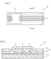
- Fluororesin base material 1 includes a fluororesin layer 2 containing a fluororesin as a main component, and a modified layer 3 formed on at least a partial region of the surface of fluororesin layer 2.
- the "surface" of fluororesin layer 2 refers to the entire peripheral surface of fluororesin layer 2, including one surface of fluororesin layer 2 and another surface opposite to that surface.
- Fig. 1 shows modified layer 3 formed on all of one surface, this is merely illustrative, and the region on which modified layer 3 is formed may be a portion of one surface, or may be all of both surfaces or a portion of each of both surfaces.
- fluororesin refers to a fluororesin in which at least one of hydrogen atoms bonded to carbon atoms forming the repeating unit of the polymer chain has been substituted with a fluorine atom or an organic group having a fluorine atom (hereinafter also referred to as a "fluorine atom-containing group").
- the fluorine atom-containing group is a group in which at least one of hydrogen atoms in a straight or branched chain organic group has been substituted with a fluorine atom, and examples may include a fluoroalkyl group, a fluoroalkoxy group, and a fluoropolyether group.
- fluoroalkyl group means an alkyl group in which at least one hydrogen atom has been substituted with a fluorine atom, and includes a "perfluoroalkyl group”. Specifically, the "fluoroalkyl group” includes a group in which all of the hydrogen atoms in an alkyl group have been substituted with fluorine atoms; a group in which all of hydrogen atoms except for one terminal hydrogen atom of an alkyl group have been substituted with fluorine atoms; etc.
- fluoroalkoxy group means an alkoxy group in which at least one hydrogen atom has been substituted with a fluorine atom, and includes a "perfluoroalkoxy group”. Specifically, the "fluoroalkoxy group” includes a group in which all of the hydrogen atoms in an alkoxy group have been substituted with fluorine atoms; a group in which all of hydrogen atoms except for one terminal hydrogen atom of an alkoxy group have been substituted with fluorine atoms; etc.
- fluoropolyether group means a monovalent group having an oxyalkylene unit as a repeating unit and having a terminal alkyl group or hydrogen atom, in which at least one hydrogen atom of the alkylene oxide chain or the terminal alkyl group has been substituted with a fluorine atom.
- fluoropolyether group includes a "perfluoropolyether group” having a plurality of perfluoroalkylene oxide chains as a repeating unit.
- unmodified fluororesin base material 1 may include polytetrafluoroethylene (PTFE), polytetrafluoroethylene-perfluoroalkylvinylether copolymer (PFA), tetrafluoroethylene-hexafluoropropylene copolymer (FEP), tetrafluoroethylene-ethylene copolymer (ETFE), polyvinylidene fluoride (PVDF), polychlorotrifluoroethylene (PCTFE), chlorotrifluoroethylene-ethylene copolymer (ECTFE), polyvinyl fluoride (PVF), as well as a thermoplastic fluororesin (THV) and a fluoroelastomer formed of the three monomers of tetrafluoroethylene, hexafluoropropylene, and vinylidene fluoride.
- PTFE polytetrafluoroethylene
- PFA polytetrafluoroethylene-perfluoroalkylvinylether copolymer
- fluororesin used as the main component of fluororesin layer 2 are tetrafluoroethylene-hexafluoropropylene copolymer (FEP), polytetrafluoroethylene-perfluoroalkylvinylether copolymer (PFA), and polytetrafluoroethylene (PTFE).
- FEP tetrafluoroethylene-hexafluoropropylene copolymer
- PFA polytetrafluoroethylene-perfluoroalkylvinylether copolymer
- PTFE polytetrafluoroethylene
- Fluororesin layer 2 can also contain, as optional component(s), an engineering plastic, a flame retardant, a flame retardant aid, a pigment, an antioxidant, a reflection imparting agent, a masking agent, a lubricant, a processing stabilizer, a plasticizer, a foaming agent, and/or a reinforcing material, for example.
- an engineering plastic e.g., a flame retardant, a flame retardant aid, a pigment, an antioxidant, a reflection imparting agent, a masking agent, a lubricant, a processing stabilizer, a plasticizer, a foaming agent, and/or a reinforcing material, for example.
- the engineering plastic to be used can be selected from known engineering plastics based on the characteristics required in fluororesin base material 1. Typically, an aromatic polyether ketone can be used as the engineering plastic.
- the aromatic polyether ketone may include polyetheretherketone (PEEK) having a structural unit in which an ether bond, a benzene ring, an ether bond, a benzene ring, a ketone bond, and a benzene ring are aligned in this order, and polyether ketone (PEK) having a repeating unit in which an ether bond, a benzene ring, a ketone bond, and a benzene ring are aligned in this order.
- PEEK is particularly preferable as the aromatic polyether ketone.
- These aromatic polyether ketones have excellent wear resistance, heat resistance, insulating properties, workability, etc.
- Aromatic polyether ketones of various grades are available in the market, and a commercially available aromatic polyether ketone may be used alone, or aromatic polyether ketones of a plurality of grades may be used in combination, or a modified aromatic polyether ketone may be used.
- any of various known flame retardants can be used, such as, for example, a halogenated flame retardant such as a brominated flame retardant or a chlorinated flame retardant.
- any of various known flame retardant aids can be used, such as, for example, antimony trioxide.
- any of various known pigments can be used, such as, for example, titanium oxide.
- antioxidant any of various known antioxidants can be used, such as, for example, a phenolic antioxidant.
- reflection imparting agent any of various known reflection imparting agents can be used, such as, for example, titanium oxide.
- the reinforcing material is not particularly limited as long as it has a linear expansion coefficient lower than that of fluororesin layer 2, the reinforcing material desirably has an insulating property, heat resistance such that it does not melt and flow at the melting point of the fluororesin, a tensile strength equal to or higher than that of the fluororesin, and corrosion resistance.
- This reinforcing material can be composed of, for example, glass cloth obtained by forming a glass into a cloth; fluororesin-containing glass cloth obtained by impregnating such glass cloth with a fluororesin; resin cloth obtained by forming a heat-resistant fiber such as a metal, a ceramic, alumina, polytetrafluoroethylene (PTFE), polyetheretherketone (PEEK), a polyimide (PI), or aramid into a cloth or a nonwoven fabric; or a heat-resistant film containing, as a main component, polytetrafluoroethylene (PTFE), a liquid crystal polymer (LCP (I type)), a polyimide, polyamidoimide (PAI), polybenzimidazole (PBI), polyetheretherketone, polytetrafluoroethylene, tetrafluoroethylene-perfluoro alkyl vinyl ether copolymer (PFA), a thermosetting resin, a crosslinkable resin, or the like.
- the above-described resin cloth or heat-resistant film to be used has a melting point (or a heat deflection temperature) not lower than a temperature of thermocompression bonding in a step of forming the modified layer described below.
- the cloth is preferably plain-woven to make fluororesin base material 1 thin, while it is preferably twill-woven or satin-woven to make fluororesin base material 1 flexible. Other known weaves are also applicable.
- Fluororesin base material 1 may be provided with a hollow structure.
- a lower limit of the average thickness of fluororesin base material 1 is preferably 3 ⁇ m, and more preferably 6 ⁇ m.
- an upper limit of the average thickness of fluororesin base material 1 is preferably 1 mm, more preferably 0.5 mm, still more preferably 0.1 mm, and particularly preferably 55 ⁇ m. If the average thickness of fluororesin base material 1 falls below the lower limit, the strength of fluororesin base material 1 may become insufficient. On the other hand, if the average thickness of fluororesin base material 1 exceeds the upper limit, the flexibility and the optical transparency of fluororesin base material 1 and thus, of a printed wiring board including fluororesin base material 1, may become insufficient.
- a lower limit of the optical transmittance at a wavelength of 600 nm of fluororesin base material 1 is preferably 50%, and more preferably 70%.
- an upper limit of the optical transmittance of fluororesin base material 1 is not particularly limited, theoretically, it does not exceed 100%. If the light transparency falls below the lower limit, fluororesin base material 1 may not be usable for applications requiring transparency.
- Examples of such applications requiring transparency may include a printed circuit board for an electrical circuit having a light emitting element that projects light or a light receiving element that receives light, through fluororesin base material 1; a hybrid circuit board including both an optical circuit and an electrical circuit; and a transparent conductive film used for, for example, a flat display panel, a touch panel, or the like including an organic EL, a liquid crystal, or the like.
- Modified layer 3 contains a siloxane bond (Si-O-Si) and a hydrophilic organofunctional group.
- Modified layer 3 is formed by causing a modifier (silane coupling agent) having a hydrophilic organofunctional group and producing a siloxane bond to be bonded to the fluororesin as the main component of fluororesin layer 2. That is, in modified layer 3, the hydrophilic organofunctional group is bonded to a Si atom forming the siloxane bond. This hydrophilic organofunctional group imparts wettability to the surface side of fluororesin base material 1.
- the chemical bond between the fluororesin and the modifier may be formed of a covalent bond alone, or may contain a covalent bond and a hydrogen bond.
- Modified layer 3 is a region believed to differ from a region (near a surface of fluororesin layer 2) excluding modified layer 3 near the surface of fluororesin base material 1, in terms of microstructure, molecular structure, and abundance ratio of elements.
- the hydrophilic organofunctional group contained in modified layer 3 makes fluororesin base material 1 hydrophilic, which improves the wettability of the surface.
- fluororesin base material 1 is surface-treated in a polar solvent, the uniformity of the treatment rate and the surface treatment (evenness of the treatment) can be improved.
- a Si atom forming the siloxane bond (this atom is hereinafter referred to as the "Si atom of the siloxane bond") is covalently bonded to a C atom of fluororesin layer 2 via at least one atom of any of N, C, O, and S atoms.
- the Si atom of the siloxane bond is bonded to the C atom of the fluororesin via an atomic group such as -O-, -S-, -S-S-, -(CH 2 )n-, -NH-, -(CH 2 )n-NH-, or -(CH 2 )n-O-(CH 2 )m- (where each of n and m is an integer of 1 or more).
- hydrophilic organofunctional group Preferable as the hydrophilic organofunctional group are a hydroxy group, a carboxy group, a carbonyl group, an amino group, an amide group, a sulfide group, a sulfonyl group, a sulfo group, a sulfonyldioxy group, an epoxy group, a methacryl group, and a mercapto group. Among these, a group containing a N atom or a S atom is more preferable.
- modified layer 3 may contain two or more types of these hydrophilic organofunctional groups.
- modified layer 3 with hydrophilic organofunctional groups exhibiting different properties, the reactivity or the like of the surface of fluororesin base material 1 can be diversified. Any of these hydrophilic organofunctional groups is bonded to a Si atom as a constituent of the siloxane bond, either directly or via one or more C atoms (for example, a methylene or phenylene group).
- a silane coupling agent having a hydrophilic organofunctional group in the molecule is suitable, and in particular, a silane coupling agent having a hydrolyzable silicon-containing functional group containing a Si atom is more suitable.
- a silane coupling agent is chemically bonded to the fluororesin forming fluororesin layer 2.
- the chemical bond between the silane coupling agent and the fluororesin of fluororesin layer 2 may be formed of a covalent bond alone, or may contain a covalent bond and a hydrogen bond.
- the term "hydrolyzable silicon-containing functional group” refers to a group that can form a silanol group (Si-OH) through hydrolysis.
- An upper limit of the contact angle of the surface of modified layer 3 with pure water is 90°, preferably 80°, and more preferably 70°. If the contact angle of the surface of modified layer 3 with pure water exceeds the upper limit, the adhesion strength to the adhered material such as the conductive pattern or the like may become insufficient. On the other hand, a lower limit of the contact angle of the surface of modified layer 3 with pure water is not particularly limited.
- modified layer 3 has etching resistance such that modified layer 3 is not removed by an etching treatment in which it is immersed under conditions of 45°C and 2 minutes, using an etchant containing iron chloride and having a specific gravity of 1.33 g/cm 3 and a free hydrochloric acid concentration of 0.2 mol/L.
- modified layer 3 is not removed means that the hydrophilicity is not lost, and the contact angle of pure water on the portion where modified layer 3 is formed does not exceed 90°. Note that although the etching treatment may sometimes unevenly produce hydrophobic minute portions in the region where modified layer 3 is formed, if the entire region has hydrophilicity, hydrophilicity is maintained in this state.
- modified layer 3 has etching resistance against an etchant containing copper chloride. Note that it has been ascertained that when modified layer 3 has the above-described etching resistance against the etchant containing iron chloride, modified layer 3 has the above-described etching resistance against an etchant containing copper chloride.
- a lower limit of an adhesion energy between the surface of modified layer 3 and water is preferably 50 dyne/cm. If the adhesion energy between the surface of modified layer 3 and water falls below the lower limit, the adherence of the surface of fluororesin base material 1 may become insufficient compared to that of pure polytetrafluoroethylene (PTFE).
- PTFE polytetrafluoroethylene
- a lower limit of wetting tension of the surface of modified layer 3 is preferably 50 mN/m, and more preferably 60 m N/m. If the wetting tension is less than the lower limit, the adhesive force may become insufficient, which may cause the adhered material to be peeled off from modified layer 3.
- the surface of modified layer 3 has improved adherence because the lower limit of the wetting tension described above is greater than the wetting tension of pure polytetrafluoroethylene (PTFE). In contrast, if the wetting tension of the surface of modified layer 3 falls below the lower limit, the adherence of the surface of modified layer 3 may become insufficient.
- wetting tension is a value measured in accordance with JIS-K-6768 (1999).
- An upper limit of the average thickness of modified layer 3 is preferably 400 nm, and more preferably 200 nm. If the average thickness of modified layer 3 exceeds the upper limit, the dielectric loss may increase in applications where fluororesin base material 1 is used as a circuit board, leading to insufficient high frequency characteristics.
- a lower limit of the peel strength of the epoxy resin adhesive having an average thickness of 25 ⁇ m against the surface of modified layer 3 is preferably 1.0 N/cm, more preferably 3.0 N/cm, and still more preferably 5.0 N/cm, as measured using a polyimide sheet having an average thickness of 12.5 ⁇ m as a flexible adherent. If the peel strength of the epoxy resin adhesive against the surface of modified layer 3 falls below the lower limit, peeling of the adhered material such as a cover lay adhered to the surface of fluororesin base material 1 cannot be prevented, and thus, reliability required in a circuit module including fluororesin base material 1 may not be achieved.
- An upper limit of mean surface roughness Ra of the surface of modified layer 3 is preferably 4 ⁇ m, more preferably 2 ⁇ m, and still more preferably 1 ⁇ m. If mean surface roughness Ra of the surface of modified layer 3 exceeds the upper limit, when a conductive pattern is laminated on the surface of modified layer 3, a rear surface of the conductive pattern may become uneven, and an electrical current may flow along this uneven portion due to the skin effect. This may lead to an increased transmission delay and transmission loss of high frequency characteristic signals, and may lead to increased scattering of light and thus, reduced transparency of fluororesin base material 1.
- Fluororesin base material 1 having the above-described structure is used as an insulating layer of a printed wiring board, for example.
- a coating member a covering resin, an adhesive, an ink, or the like is laminated on fluororesin base material 1.
- the coating member may be a cover lay film, for example.
- a cover lay is generally formed of a base material made of a resin film, and an adhesive layer that is laminated on the base material and to be adhered to fluororesin base material 1.
- the base material of such a cover lay is formed of, for example, a polyimide, an epoxy resin, SPS, a fluororesin, a crosslinkable polyolefin, or a silicone.
- Examples of the adhesive adhered to fluororesin base material 1 may include a conductive adhesive, an anisotropic conductive adhesive, an adhesive for a cover lay film, and a prepreg resin for bonding substrates together.
- resins for use as a main component of such an adhesive may include an epoxy resin, a polyimide, an unsaturated polyester, a saturated polyester, a butadiene resin, an acrylic resin, a polyamide, a polyolefin, a silicone, a fluororesin, an urethane resin, polyetheretherketone (PEEK), polyamidoimide (PAI), polyethersulfone (PES), syndiotactic polystyrene (SPS), and a resin containing one or more of the above.
- a resin obtained by crosslinking any of these resins using an electron beam, a radical reaction, or the like may also be used as the material of the adhesive.
- Fluororesin base material 1 having the above-described structure can also be used as a cover lay film of another printed wiring board.
- fluororesin base material 1 having the above-described structure can be used as a cover lay film for a printed wiring board having fluororesin base material 1 as an insulating layer. That is, the low dielectric material isadopted for both the insulating layer and the coating material. With this structure, a high frequency circuit module with a low signal transmission loss can be achieved. Note that in this case, because the insulating layer and the cover lay film are both made of the fluororesin, they can be adhered to each other by thermal fusion, without using an adhesive. This pressing is performed under conditions of not lower than 180°C and not higher than 400°C, not shorter than 20 minutes and not longer than 30 minutes, and not lower than 3 MPa and not higher than 4 MPa.
- Fluororesin base material 1 can also be adopted as a cover lay film for a printed wiring board having a polyimide or a liquid crystal polymer as an insulating layer.
- the printed wiring board and fluororesin base material 1 are adhered to each other with an adhesive sandwiched therebetween.
- fluororesin base material 1 includes modified layer 3, with this side serving as the surface to be adhered, fluororesin base material 1 and the printed wiring board can be bonded to each other with an existing adhesive (for example, an epoxy resin).
- a printed wiring board 10 according to one embodiment of the present invention will be described.
- Printed wiring board 10 includes fluororesin base material 1 having the above-described structure, and a conductive pattern 11 formed on at least one surface of fluororesin base material 1. Conductive pattern 11 is formed on at least a partial region of fluororesin base material 1. Conductive pattern 11 is at least partially covered with a coating material 13. Note that coating material 13 may not be provided, depending on the application of printed wiring board 10.
- modified layer 3 is formed to include a region having conductive pattern 11 and coating material 13 in fluororesin base material 1. That is, preferably, conductive pattern 11 is provided on modified layer 3, and coating material 13 is provided on modified layer 3. With this structure, the peel strength of conductive pattern 11 and coating material 13 is improved.
- Conductive pattern 11 is formed of, for example, copper, silver, gold, SUS (stainless steel), iron, aluminum, nickel, or ITO (Indium Tin Oxide). Conductive pattern 11 may also be formed of a conductive resin or conductive adhesive, which is a mixture of a resin and a metal powder. Note that conductive pattern 11 includes a land, a ground pattern, an electrode, a metal reinforcing layer, a dummy layer, and the like.
- Coating material 13 includes a coating member such as a cover lay film, and a covering resin having fluidity when uncured.
- the covering resin may include a coating resin, solder resist, a conductive adhesive, an electromagnetic shielding material, a heat conductive material, a reinforcing agent, an adhesive, a tackifier, an adhesive for a cover lay film, an ink, and a conductive paste.
- Examples of materials of these covering resins may include an epoxy resin, a polyimide, an unsaturated polyester, a saturated polyester, a butadiene resin, an acrylic resin, a polyamide, a polyolefin, a silicone, a fluororesin, an urethane resin, polyetheretherketone, polyamidoimide, polyethersulfone, syndiotactic polystyrene, a styrene-based resin, modified polyphenylene ether (m-PPE), and a resin containing two or more of the above.
- a resin obtained by mixing a styrene-based resin and modified polyphenylene ether is preferable because of its low dielectric constant and ease of adhesion.
- a resin obtained by crosslinking any of these resins using an electron beam, a radical reaction, or the like may also be used as the material of the covering resin.
- a resin obtained by including voids or bubbles (vacancies) in any of these resins may also be used as the material of the covering resin.
- a resin having high adhesiveness to the fluororesin forming fluororesin base material 1 is preferable among the resins mentioned above.
- this resin may include a fluororesin, polyetheretherketone, polyamidoimide, polyethersulfone, an epoxy resin, an acrylic resin, a polyamide, an urethane resin, a styrene-based resin, and modified polyphenylene ether.
- the dielectric constant ⁇ can be set to 3 or less in coating material 13 formed of a fluororesin, a crosslinkable polyolefin, a styrene-based resin such as syndiotactic polystyrene, or modified polyphenylene ether, or coating material 13 having voids or bubbles (vacancies) in any of the above.
- Coating material 13 having this structure is therefore suitable as a member requiring a low dielectric loss (for example, a member for high frequency use).
- Fig. 3 is a cross-sectional view along A-A in Fig. 2 of printed wiring board 10.
- a cover lay film as coating material 13 includes an adhesive layer 14 and a protective layer 15. Conductive pattern 11 is formed on modified layer 3. Adhesive layer 14 of the cover lay film is adhered to modified layer 3. This allows the cover lay film to be resistant to peeling.
- Fig. 4 illustrates another example of the printed wiring board.
- a printed wiring board 10X includes fluororesin base material 1 described above. Modified layer 3 is formed on one surface of printed wiring board 10X. That is, the one surface is made hydrophilic. Conductive pattern 11 is also formed on the surface on which modified layer 3 is formed. At least a central portion 16 is transparent, and mean surface roughness Ra of central portion 16 is formed to be 4 ⁇ m or less.
- Printed wiring board 10X is used as an electrode sheet for a touch panel, for example. Note that modified layer 3 may be formed on all of, or one or more partial regions of, the other surface of printed wiring board 10X.
- printed wiring board 10X when printed wiring board 10X is transferred on a transfer plate, printed wiring board 10X is adsorbed onto the transfer plate by virtue of the function of modified layer 3 formed on the other surface. This suppresses slippage of printed wiring board 10X during transfer.
- Circuit module 20 includes printed wiring board 10 described above, and an electronic component 21 mounted on printed wiring board 10. Conductive pattern 11 connected to electronic component 21 is covered with coating material 13 such as solder resist or a cover lay film.
- Examples of electronic component 21 may include a resistor, a capacitor, a coil, a connector, a switch, an IC (Integrated Circuit), a light emitting element, a light receiving element, an acceleration sensor, an acoustic device (a piezoelectric element, a silicon microphone, or the like), a magnetic sensor, a temperature sensor, and a coaxial cable.
- Circuit module 20 is superior in manufacturability to a circuit module having a conventional fluororesin base material, in that printed wiring board 10 described above includes fluororesin base material 1 having heat resistance that withstands reflow, and having modified layer 3 with high adhesiveness. Circuit module 20 has also excellent heat resistance because it has fluororesin base material 1 with high heat resistance.
- the high frequency circuit module includes printed wiring board 10 described above, and a high frequency device (a kind of electronic component 21) mounted on printed wiring board 10. Conductive pattern 11 connected to electronic component 21 is covered with coating material 13 such as solder resist or a cover lay film.
- This high frequency circuit module which includes fluororesin base material 1 having a low dielectric constant, provides a reduced signal transmission loss of high frequency signals, compared to a high frequency circuit module having an epoxy resin base material.
- conductive pattern 11 and solder resist are provided on modified layer 3. This makes conductive pattern 11 and solder resist resistant to peeling from fluororesin base material 1 even in a high temperature, high humidity environment. This suppresses disconnection due to peeling of conductive pattern 11, or deterioration of circuit characteristics due to peeling of the solder resist, even in a high temperature, high humidity environment. Consequently, deterioration of the characteristics of the high frequency circuit module can be reduced, compared with a high frequency circuit module having a conventional fluororesin base material without modified layer 3.
- a primer material 101 containing a silane coupling agent as the modifier, an alcohol, and water is adhered to a flat plate-like carrier 100 (see Fig. 6(A) ).
- a region of a surface of carrier 100 to which primer material 101 is to be adhered is at least a portion of the surface of carrier 100, and primer material 101 may be adhered to the entire surface of carrier 100.
- Primer material 101 may be adhered to only one surface of carrier 100, or only a partial region of one surface of carrier 100.
- the entire surface of carrier 100 herein means the entire outer peripheral surface.
- the entire surface of carrier 100 means all of the opposite surfaces, and when carrier 100 is rectangular, it means all of the six surfaces.
- Primer material 101 may be adhered to carrier 100 using any non-limiting method. For example, any of an immersion method, a spraying method, a coating method, and the like may be adopted.
- the alcohol in primer material 101 is then removed by drying.
- the alcohol may be removed using any of natural drying, heat drying, and drying under reduced pressure. Note that drying may be continuously performed in a press machine 900 that performs thermocompression bonding in a second step. After drying, the silane coupling agent is bonded to carrier 100 by heating (at 120°C for 15 minutes, for example).
- a lower limit of the content of the silane coupling agent in the entire primer material 101 is preferably 0.1 mass%, and more preferably 0.5 mass%.
- an upper limit of the content of the silane coupling agent in the entire primer material 101 is preferably 5 mass%, and more preferably 3 mass%. If the content of the silane coupling agent exceeds the upper limit, aggregation of the silane coupling agent may occur, and a film of primer material 101 with a uniform thickness may not be easily formed on the surface of carrier 100.
- silane coupling agent a silane coupling agent having a hydrophilic organofunctional group containing a N atom or a S atom and having a hydrolyzable silicon-containing functional group containing a Si atom is suitably used.
- the hydrolyzable silicon-containing functional group containing a Si atom of the silane coupling agent produces a silanol group through hydrolysis. Further, condensation of these silanol groups forms a siloxane bond (Si-O-Si). Moreover, some of the silanol groups and the hydrophilic organofunctional groups are bonded to carrier 100. As a result, a coating containing siloxane bonds that ensure stability and the hydrophilic organofunctional groups that ensure hydrophilicity is formed on carrier 100. Furthermore, the hydrophilic organofunctional group, which contains a N atom or a S atom, can be relatively easily bonded to the fluororesin of fluororesin layer 2.
- the above-described hydrolyzable silicon-containing functional group containing a Si atom is specifically a group in which an alkoxy group is bonded to the Si atom.
- the alkoxy group may include a methoxy group, an ethoxy group, a propoxy group, a t-butoxy group, and a pentyloxy group.
- hydrophilic organofunctional group containing a N atom may include an amino group and an ureido group.
- silane coupling agents having the hydrophilic organofunctional group containing a N atom may include an aminoalkoxysilane, an ureidoalkoxysilane, and derivatives thereof.
- aminoalkoxysilane may include 3-aminopropyltrimethoxysilane, 3-aminopropyltriethoxysilane, N-(2-aminoethyl)-3-aminopropylmethyldimethoxysilane, N-(2-aminoethyl)-3-aminopropyltrimethoxysilane, N-(2-aminoethyl)-3-aminopropyltriethoxysilane, and N-phenyl-3-aminopropyltrimethoxysilane.
- Examples of derivatives of the aminoalkoxysilane may include a ketimine such as 3-triethoxysilyl-N-(1,3-dimethyl-butylidene)propylamine, and a salt of a silane coupling agent such as N-vinylbenzyl-2-aminoethyl-3-aminopropyltrimethoxysilane acetate.
- a ketimine such as 3-triethoxysilyl-N-(1,3-dimethyl-butylidene)propylamine
- a salt of a silane coupling agent such as N-vinylbenzyl-2-aminoethyl-3-aminopropyltrimethoxysilane acetate.
- ureidoalkoxysilane examples include 3-ureidopropyltriethoxysilane, 3-ureidopropyltrimethoxysilane, and N-(2-ureidoethyl)-3-aminopropyltrimethoxysilane.
- hydrophilic organofunctional group containing a S atom may include a mercapto group and a sulfide group.
- silane coupling agents having the hydrophilic organofunctional group containing a S atom may include mercaptoalkoxysilane, sulfidealkoxysilane, and derivatives thereof.
- Examples of the mercaptoalkoxysilane may include 3-mercaptopropyltrimethoxysilane, 3-mercaptopropyltriethoxysilane, and 3-mercaptopropyl(dimethoxy)methylsilane.
- sulfidealkoxysilane my include bis(3-triethoxysilylpropyl)tetrasulfide and bis(3-triethoxysilylpropyl)disulfide.
- a silane coupling agent obtained by introducing a modifier group to any of the above-described silane coupling agents may also be used.
- a phenyl group is preferable as the modifier group.
- silane coupling agent is 3-aminopropyltriethoxysilane, N-phenyl-3-aminopropyltrimethoxysilane, 3-ureidopropyltriethoxysilane, 3-mercaptopropyltrimethoxysilane, or bis(3-triethoxysilylpropyl)tetrasulfide.
- another coupling agent can be used as a modifier.
- Any coupling agent that is reactive with the fluororesin of fluororesin layer 2 or radicals thereof may be used as the other coupling agent, such as, for example, a titanium-based coupling agent.
- titanium-based coupling agent may include isopropyltriisostearoyl titanate, isopropyltristearoyl titanate, isopropyltrioctanoyl titanate, isopropyldimethacrylisostearoyl titanate, isopropyltridodecylbenzenesulfonyl titanate, isopropylisostearoyldiacryl titanate, isopropyltri(dioctylphosphate)titanate, isopropyltricumylphenyl titanate, isopropyltris(dioctylpyrophosphate)titanate, isopropyltri(N-aminoethyl-aminoethyl)titanate, tetraisopropylbis(dioctylphosphite)titanate, tetraoctylbis(ditridecylphos
- Examples of the alcohol contained in primer material 101 may include methanol, ethanol, n-propanol, n-butanol, tert-butanol, and isopropyl alcohol.
- a solution containing one or more selected from the group consisting of these alcohols is used as a solvent of primer material 101.
- Water in primer material 101 which may be used in a very small amount, is essential for the condensation of the silane coupling agent.
- the proportion of water is set to, for example, not less than 0.01 mass% and not more than 0.1 mass%, based on the total amount of the alcohol.
- carrier 100 is formed of a metal such as copper, gold, silver, iron, aluminum, or nickel, or a material such as a glass, silicon, a silicone, carbon, or a ceramic. Carrier 100 may also be a composite of these materials.
- a base metal that dissolves in an etchant is adopted as carrier 100.
- a metal sheet such as copper, iron, or aluminum is used as carrier 100 of primer material 101.
- base metal refers to a metal having an ionization tendency equal to or higher than that of copper, and specifically, a metal having a standard redox potential of 0.5 V or less.
- carrier 100 is not particularly limited, it is configured to match the shape of the object on which modified layer 3 is to be formed.
- plate-like carrier 100 is used.
- carrier 100 shaped to conform to the curved surface is used.
- Carrier 100 may also be segmented into a plurality of block regions when seen in a plan view.
- mean surface roughness Ra of a portion of carrier 100 to which primer material 101 is adhered (hereinafter referred to as the "adhered surface") is set to be not more than a predetermined value.
- an upper limit of mean surface roughness Ra of the adhered surface of carrier 100 is preferably 4 ⁇ m, and more preferably 1 ⁇ m. If mean surface roughness Ra of the adhered surface of carrier 100 exceeds the upper limit, mean surface roughness Ra of modified layer 3 may become high. It is also desirable to adjust the adhered surface of carrier 100 to achieve a surface on which a liquid primer material can be uniformly applied.
- the adhered surface of carrier 100 advantageously has good wettability, and desirably has a contact angle of 100° or less with water.
- mean surface roughness Ra of a predetermined region of the entire adhered surface of carrier 100 may be set to not more than a predetermined value, and mean surface roughness Ra of a peripheral portion of the predetermined region may be set to be higher than the predetermined value.
- the surface roughness of modified layer 3 of the portion corresponding to the predetermined region can be made lower than the surface roughness of the peripheral portion thereof.
- fluororesin material 102 is laminated onto the surface of carrier 100 on which the primer material is adhered, with primer material 101 sandwiched therebetween, and the resulting laminate is subjected to thermocompression bonding with press machine 900 (see Fig. 6(B) ).
- Thermocompression bonding is preferably performed under reduced pressure, in order to prevent bubbles or voids from being formed between carrier 100 and fluororesin material 102.
- Thermocompression bonding is also preferably performed under low oxygen conditions, in order to suppress oxidation of carrier 100.
- thermocompression bonding is performed in a nitrogen atmosphere. In this way, modified layer 3 is formed between carrier 100 and fluororesin material 102.
- Fluororesin material 102 is a member forming fluororesin layer 2 of fluororesin base material 1. Depending on the application of fluororesin base material 1, fluororesin material 102 containing any of various additives (filler) is used. When a bending strength is required in fluororesin base material 1, fluororesin material 102 containing the above-described reinforcing material such as glass cloth is used.
- thermocompression bonding is performed under the following conditions.
- Thermocompression bonding is preferably performed at a temperature not lower than the melting point (more preferably, not lower than a decomposition start temperature) of fluororesin material 102, and not higher than a decomposition temperature of fluororesin material 102.
- the term "decomposition start temperature” refers to a temperature at which fluororesin material 102 begins to undergo thermal decomposition
- the term “decomposition temperature” refers to a temperature at which fluororesin material 102 undergoes a 10% decrease in mass due to the thermal decomposition.
- thermocompression bonding is performed at a temperature not lower than the melting point of fluororesin material 102 is that fluororesin material 102 will not be activated at a temperature lower than the melting point. Furthermore, the temperature is set to not lower than the decomposition start temperature of fluororesin material 102, because the C atoms in fluororesin material 102 are converted into radicals, which further activates fluororesin material 102. That is, it is believed that when the temperature of thermocompression bonding is not lower than the melting point of fluororesin material 102, preferably not lower than the decomposition start temperature, bonding of the fluororesin to the layer formed on carrier 100 with the silane coupling agent can be accelerated.
- a lower limit of the temperature of thermocompression bonding of fluororesin material 102 is preferably a temperature that is 30°C higher, and more preferably 50°C higher, than the melting point of fluororesin material 102.
- thermocompression bonding is preferably performed at a temperature of 300°C or higher, and more preferably 320°C or higher.
- an upper limit temperature of thermocompression bonding is 600°C, and more preferably 500°C. This allows decomposition of fluororesin material 102 to be suppressed.
- the pressure is set to not less than 0.01 MPa and not more than 100.0 MPa.
- the pressurization time is not shorter than 0.01 minute and not longer than 1000 minutes.
- the pressure and the pressurization time are not restricted, and are set in consideration of the reactivity or the like of the silane coupling agent.
- thermocompression bonding it is believed that a C atom in radical form of the fluororesin of fluororesin material 102 is chemically bonded to the siloxane bond (Si-O-Si) formed with the silane coupling agent via another atom or atomic group.
- modified layer 3 is a polymer that spreads like a film, and there is a possibility that this polymer and the fluororesin may be strongly bonded to each other with multiple hydrogen bonds being formed between them. Thus, the possibility that these hydrogen bonds and the covalent bond are both present is not excluded.
- modified layer 3 is exposed by removing at least a portion of carrier 100 (see Fig. 6(C) ).
- the dissolution method or a stripping method may be used to remove carrier 100.
- carrier 100 is a sheet made of a base metal
- the dissolution method is adopted, because a metal sheet is difficult to strip from fluororesin material 102.
- the laminate of carrier 100 and fluororesin material 102 is immersed in a solution that dissolves the above-described base metal, thereby completely removing carrier 100.
- carrier 100 When a copper material is used as carrier 100, carrier 100 (copper) of the laminate is dissolved in an etchant.
- an etchant is suitably used that contains iron chloride or copper chloride, and having a specific gravity not less than 1.31 g/cm 3 and not more than 1.33 g/cm 3 and a free hydrochloric acid concentration not less than 0.1 mol/L and not more than 0.2 mol/L.
- etching is preferably performed under conditions such that the temperature is not lower than 30°C and not higher than 45°C, and the immersion time is not shorter than 30 seconds and not longer than 2 minutes. Under these conditions, the copper foil can be removed, and the removal of modified layer 3 from fluororesin material 102 can be suppressed.
- carrier 100 a carrier that is easily stripped from fluororesin material 102 after the thermocompression bonding between carrier 100 and fluororesin material 102 is adopted as carrier 100.
- carrier 100 a silicone sheet or a metal foil is used as carrier 100.
- carrier 100 segmented into a plurality of block regions when seen in a plan view may be used, and at least a portion of the plurality of block regions may be stripped.
- carrier 100 simplifies the work of the third step. That is, carrier 100 can be removed from fluororesin material 102 without performing the dissolution treatment. While the stripping method may also be described as a transfer method, it differs from simple transfer in that during transfer, primer material 101 is altered in properties and bonded to fluororesin material 102.
- the fluororesin has low wettability, if a method in which a liquid reactant is directly applied to the surface of fluororesin material 102 is used, the reactant will be unevenly distributed and thus, it is difficult to introduce the hydrophilic organofunctional groups evenly to the surface of fluororesin material 102.
- a plasma method has been used to modify fluororesin material 102. With plasma, radical species can be easily formed on the surface of fluororesin material 102, which facilitates introduction of hydrophilic groups to the surface of fluororesin material 102.
- the surface state of the plasma-treated fluororesin material 102 is unstable and thus, the surface thereof gradually returns to its original stable state (surface inactive state). The plasma treatment is therefore disadvantageous in that the surface-modified state of fluororesin material 102 cannot be maintained over a long period of time.
- primer material 101 containing a silane coupling agent, an alcohol, and water is adhered to carrier 100. Because the surface of carrier 100 has good wettability, primer material 101 in liquid state is evenly applied to the surface of carrier 100.
- carrier 100 spreads in the form of a film because of the hydrophilic organofunctional group of the silane coupling agent contained in primer material 101. Then, carrier 100 in this state is heated at a temperature around 120°C to hydrolyze the hydrolyzable silicon-containing functional group containing a Si atom to produce a silanol group. This silanol group is then condensed with another silanol group to form a siloxane bond. Simultaneously, some of the silanol groups and the hydrophilic organofunctional groups are bonded to carrier 100. As a result, it is believed that a polymer film is formed in which the siloxane bond structure is two-dimensionally aligned in a network form.
- carrier 100 and fluororesin material 102 are laminated with primer material 101 being sandwiched between carrier 100 and fluororesin material 102.
- Carrier 100 and fluororesin material 102 are then subjected to thermocompression bonding at a temperature not lower than the melting point of fluororesin material 102.
- primer material 101 spreads in the form of a film on carrier 100, it does not become uneven owing to the water repellency of the fluororesin when brought into contact with fluororesin material 102. This may also be attributed to the fact that siloxane bonds are formed during drying and heating of primer material 101, in addition to the fact that primer material 101 is film-shaped. Primer material 101 is thus pressed against fluororesin material 102 with a substantially uniform thickness (with little unevenness).
- thermocompression bonding between fluororesin material 102 and carrier 100 at a temperature not lower than the melting point of fluororesin material 102 it is believed that a C atom of the fluororesin is bonded to the siloxane bond formed with the silane coupling agent via another atom or atomic group.
- a method for manufacturing printed wiring board 10 is similar to the above-described method for manufacturing fluororesin base material 1 described above. Thus, the method for manufacturing printed wiring board 10 will be described referring to the above-described method for manufacturing fluororesin base material 1.
- primer material 101 is adhered to a metal sheet as carrier 100.
- Primer material 101 contains a silane coupling agent, an alcohol, and water. This step is similar to the first step in the method for manufacturing fluororesin base material 1.
- a second step the alcohol in primer material 101 adhered to carrier 100 is removed by drying, and then carrier 100 is heated. Carrier 100 and fluororesin material 102 are then laminated with primer material 101 sandwiched therebetween, and are subjected to thermocompression bonding. This step is similar to the second step in the method for manufacturing fluororesin base material 1.
- a wiring pattern is formed similarly to an etching method adopted in a conventional method for manufacturing a printed wiring board.
- a resist pattern is formed on the metal layer as carrier 100, the laminate (laminate of carrier 100, the metal layer, and the resist pattern) is immersed in an etchant, and then the resist pattern is removed. Consequently, conductive pattern 11 is formed.
- This printed wiring board 10 in which modified layer 3 is exposed on the surface can make the adhered material such as solder resist, a conductive adhesive, or a cover lay film resistant to peeling, compared to a conventional printed wiring board.
- a feature of the method for manufacturing fluororesin base material 1 and the method for manufacturing printed wiring board 10 is that fluororesin material 102 is not subjected to a plasma treatment or alkali treatment. That is, fluororesin base material 1 or printed wiring board 10 having a surface active state can be manufactured without such a treatment. Furthermore, with this manufacturing method, modified layer 3 can be provided in a relatively simple manner on the surface of fluororesin base material 1 or printed wiring board 10.
- Fluororesin base material 1 is fluororesin base material 1 containing a fluororesin as a main component, the fluororesin base material including modified layer 3 on at least a partial region of a surface thereof, modified layer 3 containing a siloxane bond and a hydrophilic organofunctional group, and a surface of modified layer 3 having a contact angle of 90° or less with pure water. Fluororesin base material 1 is therefore highly reactive. Fluororesin base material 1 is therefore surface active. Moreover, modified layer 3 is stable over time because of its siloxane bonds. That is, fluororesin base material 1 with the above-described structure has a surface-modified state (surface active state) more stable than that of a conventional fluororesin base material.
- a peel strength of an epoxy resin adhesive having an average thickness of 25 ⁇ m against the surface of the modified layer is 1.0 N/cm or more, as measured using a polyimide sheet having an average thickness of 12.5 ⁇ m as a flexible adherent.
- the coating material laminated on the surface of the polyimide sheet or the like can be resistant to peeling from fluororesin base material 1. More preferably, the peel strength is 5.0 N/cm or more.
- modified layer 3 is preferably not removed by an etching treatment in which the modified layer is immersed under conditions of 45°C and 2 minutes, using an etchant containing iron chloride and having a specific gravity of 1.33 g/cm 3 and a free hydrochloric acid concentration of 0.2 mol/L.
- an etchant containing iron chloride and having a specific gravity of 1.33 g/cm 3 and a free hydrochloric acid concentration of 0.2 mol/L With this structure, the surface-modified state (surface activity) of fluororesin base material 1 can be maintained even if fluororesin base material 1 on which a metal layer is formed is subjected to the etching treatment. Therefore, when fluororesin base material 1 is subjected to any of various treatments after the etching treatment, it can provide a satisfactory condition after the treatment.
- a solder resist application treatment and an adhesive application treatment for fluororesin base material 1 are typically performed after etching. Because modified layer 3 is maintained even after fluororesin base material 1 is subjected to the etching treatment, the peel strength of these adhered materials (the solder resist and the adhesive) has a sufficiently high value.
- the surface of modified layer 3 preferably has a mean surface roughness Ra of 4 ⁇ m or less.
- Ra surface roughness of the bonded surface of the conductive pattern laminated on the surface of the modified layer. This reduces the unevenness of a portion where high frequency signals are concentrated due to the skin effect, allowing an electrical current to flow linearly, thus leading to a reduced transmission delay and transmission loss.
- modified layer 3 preferably has an average thickness of 400 nm or less. With this structure, when fluororesin base material 1 is used as a circuit board, deterioration of high frequency characteristics due to a dielectric loss attributed to a high dielectric constant of modified layer 3 can be suppressed.
- the bond between modified layer 3 and fluororesin layer 2 contains a chemical bond. That is, preferably, this bond is either formed of a covalent bond alone, or contains both a hydrogen bond and a covalent bond, rather than being a bond formed through physical action simply owing to an anchor effect resulting from the uneven shape of the boundary between modified layer 3 and fluororesin layer 2. With this structure, the bond between modified layer 3 and the fluororesin becomes stronger than a bond formed between modified layer 3 and fluororesin layer 2 simply through physical action.
- fluororesin base material 1 can maintain the surface-modified state over a long period of time, compared to a fluororesin base material in which modified layer 3 is adhered to the fluororesin simply through physical action owing to the anchor effect or the like.
- the hydrophilic organofunctional group is at least one selected from the group consisting of a hydroxy group, a carboxy group, a carbonyl group, an amino group, an amide group, a sulfide group, a sulfonyl group, a sulfo group, a sulfonyldioxy group, an epoxy group, a methacryl group, and a mercapto group.
- Printed wiring board 10 preferably includes fluororesin base material 1 described above. With this structure, the adhered material can be resistant to peeling in printed wiring board 10.
- the adhered material such as conductive pattern 11, solder resist, a conductive adhesive, an adhesive for fixing a component, or a cover lay film can be resistant to peeling.
- Printed wiring board 10 has conductive pattern 11 laminated on at least a portion of the region having modified layer 3 of fluororesin base material 1. That is, conductive pattern 11 is adhered to fluororesin layer 2 with modified layer 3 sandwiched therebetween. Consequently, peeling of conductive pattern 11 can be suppressed.
- the coating material (the covering resin or coating member) is preferably laminated on the surface of modified layer 3.
- the peel strength of the coating material can be higher than that when the coating material is directly adhered to the fluororesin.
- Circuit module 20 has printed wiring board 10 described above. With this circuit module 20, the presence of modified layer 3 suppresses peeling of the adhered material adhered to printed wiring board 10, leading to higher reliability of circuit module 20. Moreover, circuit module 20, which has printed wiring board 10 described above, is superior in manufacturability to a circuit module having a conventional fluororesin base material. Furthermore, circuit module 20 is superior in heat resistance to a circuit module having a conventional epoxy resin base material.
- the method for manufacturing fluororesin base material 1 includes a first step of adhering primer material 101 containing the silane coupling agent to flat-shaped carrier 100; and a second step of bonding fluororesin material 102 containing a fluororesin as a main component by thermocompression bonding to the surface of carrier 100 on which primer material 101 is adhered. With this method, fluororesin base material 1 having carrier 100 (the metal layer, for example) is formed.
- modified layer 3 having a relatively uniform thickness with little unevenness can be formed on fluororesin material 102, compared to the case where primer material 101 is directly applied to the fluororesin. Furthermore, modified layer 3 is stable over time because as a result of thermocompression bonding, the silane coupling agent is bonded together to form a siloxane bond. That is, with this manufacturing method, fluororesin base material 1 having a stable surface-modified state can be manufactured.
- carrier 100 is a metal, a glass, a silicone, carbon, a ceramic, or a composite thereof, and the silane coupling agent has the hydrolyzable silicon-containing functional group and the hydrophilic organofunctional group.
- the silane coupling agent having the hydrophilic organofunctional group is easily spread on carrier 100 in the form of a film.
- the hydrolyzable silicon-containing functional group of the silane coupling agent produce a silanol, which then condenses with another silanol to form a siloxane bond.
- Modified layer 3 containing the siloxane bond is thus formed as a layer between carrier 100 and the fluororesin, which increases the resistance of modified layer 3 to a chemical treatment such as etching. Moreover, because modified layer 3 contains the hydrophilic organofunctional group derived from the silane coupling agent, it has high adhesiveness to carrier 100 and coating material 13 that is to be laminated after the carrier is stripped.
- the hydrophilic organofunctional group contains a N atom or a S atom. Because the N atom or S atom is likely to be bonded to a C atom in radical form of the fluororesin, the hydrophilic organofunctional group containing the N or S atom is more likely to be bonded to the fluororesin than other functional groups (a group containing C and H only, such as a phenyl group). Consequently, the adhesion strength (that is, the peel strength) between modified layer 3 and the fluororesin can be increased.
- the method for manufacturing fluororesin base material 1 further includes, after the second step, a third step of removing at least a portion of carrier 100 described above.
- a third step of removing at least a portion of carrier 100 described above allows fluororesin base material 1 to be provided in which modified layer 3 is at least partially exposed.
- fluororesin base material 1 not having carrier 100 can be manufactured by completely removing carrier 100.
- the above-described dissolution method that is, a method of exposing modified layer 3 by dissolving carrier 100 with a solution that dissolves the base metal, can be adopted in the third step.
- the dissolution method can use a conventional etching method for removing carrier 100.
- any section of carrier 100 can be removed similarly to the conventional etching method to expose any section of modified layer 3.
- a method of exposing modified layer 3 by stripping any of the blocks of carrier 100 from fluororesin material 102 can be used in the third step.
- carrier 100 is removed by being stripped from fluororesin material 102, the manufacturing process of fluororesin base material 1 can be more simplified than the case where carrier 100 is removed by dissolution.
- the method for manufacturing printed wiring board 10 includes a first step of adhering primer material 101 containing the silane coupling agent to carrier 100; a second step of bonding fluororesin material 102 containing a fluororesin as a main component by thermocompression bonding to the surface of carrier 100 on which primer material 101 is adhered; and a third step, after the second step, of forming a circuit (conductive pattern 11) by removing a portion of carrier 100 with an etchant.
- modified layer 3 having a relatively uniform thickness with little unevenness can be formed on fluororesin material 102, compared to the case where primer material 101 is directly applied to the fluororesin. Furthermore, modified layer 3 is stable over time because as a result of thermocompression bonding, the silane coupling agent is bonded together to form a siloxane bond. That is, with this structure, printed wiring board 10 having a stable surface-modified state can be manufactured.
- carrier 100 is copper
- the etchant used in the third step contains iron chloride or copper chloride.
- a circuit pattern can be formed similarly to a conventional method.
- the temperature of the thermocompression bonding in the second step is not higher than the decomposition temperature of the fluororesin of the fluororesin material. This allows decomposition of fluororesin material 102 to be suppressed in the manufacturing process.
- the method further includes the step of laminating coating material 13 onto at least a portion of a circuit-side surface of the laminate containing fluororesin 102, modified layer 3, and the circuit (conductive pattern 11).
- coating material 13 which leads to improved reliability or an increased bending strength. That is, because metal carrier 100 is covered with coating material 13, the circuit pattern formed by carrier 100 is protected against oxidation and the like. Furthermore, because modified layer 3 is covered with coating material 13, the bending strength of that portion is increased.
- Table 1 shows results of a peel strength test for fluororesin base materials 1 according to the present embodiments and comparative fluororesin base materials.
- Samples (samples 1 and 2) for use in this test were formed as follows.
- FEP having an average thickness of 0.05 mm, a dimensional width of 10 mm, and a length of 500 mm
- FEP-NE-2 from Daikin Industries, Ltd.
- Modified layer 3 was formed as follows. An aminosilane was used as a silane coupling agent for primer material 101. Ethanol was used as an alcohol for primer material 101. Water was not added. That is, water present in air and water contained in the alcohol as an impurity was used. The concentration of the silane coupling agent was 1 mass% based on the total mass of primer material 101. A copper foil (average thickness: 18 ⁇ m, mean surface roughness Ra: 0.6 ⁇ m) was used as carrier 100. Primer material 101 was adhered to the copper foil as carrier 100 using the immersion method, dried, and heated at 120°C. A layer of primer material 101 was thus formed on the copper foil. This copper foil was then bonded to the fluororesin sheet by thermocompression bonding. All of the copper foil was then removed with an etchant. A modified layer thus formed had an average thickness of 30 nm, as measured with an electron microscope.
- etching was performed under conditions of a temperature of 45°C and an immersion time of 2 minutes, with an etchant containing iron chloride adjusted to give a specific gravity not less than 1.31 g/cm 3 and not more than 1.33 g/cm 3 and a free hydrochloric acid concentration not less than 0.1 mol/L and not more than 0.2 mol/L.
- Sample 1 was washed with water after the etching treatment and dried. Immediately after that, fluororesin base material 1 was coated with a test polyimide sheet having an epoxy resin adhesive layer with an average thickness of 25 ⁇ m and a polyimide layer with an average thickness of 12.5 ⁇ m.
- CM type from Arisawa Manufacturing Co., Ltd. which uses "Apical (registered trademark) NPI” from Kaneka Corporation as the polyimide sheet was used. After the passage of 24 hours, the peel strength of the test polyimide sheet was measured.
- the peel strength (hereinafter referred to as the test polyimide sheet peel strength) was measured using the method in accordance with JIS-K-6854-2 (1999): "Adhesives - Determination of peel strength of adhered assemblies - Part 2: 180° peel”.
- Sample 2 was washed with water after the etching treatment, dried, and then left standing in an air atmosphere over 1 week. Fluororesin base material 1 was then coated with the test polyimide sheet. After the passage of 24 hours, the test polyimide sheet peel strength was measured.
- the above-described fluororesin sheet (FEP having an average thickness of 0.05 mm, an average width of 10 mm, and an average length of 500 mm ("FEP-NE-2" from Daikin Industries, Ltd.)) was plasma-treated.
- N 2 was used as a carrier gas.
- CF 4 and O 2 were used as reactant gases.
- the volume ratio of the carrier gas to the reactant gases was 1650/1000 (carrier gas/reactive gases).
- the plasma treatment was performed for 30 minutes with a capacitively coupled plasma device, at a gas pressure of 27 Pa, a flow rate of 1650 sccm, and power of 5000 W.
- the (plasma-treated) fluororesin base material was coated with the test polyimide sheet. After the passage of 24 hours, the test polyimide sheet peel strength was measured.
- the change ratio shown in Table 1 is a value calculated in accordance with ⁇ (PB - PA)/PA ⁇ ⁇ 100 (%).
- each of "PA” and “PB” represents the following.
- PA represents the test polyimide sheet peel strength measured as follows. After the formation of the modified layer on the fluororesin sheet to be tested, the fluororesin sheet was washed and dried. Immediately after that, the test polyimide sheet was adhered to the fluororesin sheet. After the passage of 24 hours, the peel strength was measured.
- "PB” represents the test polyimide sheet peel strength measured as follows. After the formation of the modified layer on the fluororesin sheet to be tested, the fluororesin sheet was washed and dried. The fluororesin sheet was left standing in an air atmosphere over 1 week, and then the test polyimide sheet was adhered to the fluororesin sheet. After the passage of 24 hours, the peel strength was measured.
- fluororesin base material 1 according to the present embodiment has adhesiveness not only to the epoxy resin adhesive but also to an adhesive containing as a main component a polyimide, a polyester, a polyamide, or the like, and substantially maintains its adhesiveness even after the passage of 1 week. That is, fluororesin base material 1 according to the present embodiment shows little decrease in surface activity even after being left standing over 1 week.
- the contact angle of pure water on the surface of the modified layer of sample 1 of the fluororesin base material was found to be distributed within the range not less than 50° and not more than 90°.
- the contact angle of pure water on the surface of the fluororesin sheet not having the modified layer was found to be distributed within the range not less than 95° and not more than 130°. Therefore, the fluororesin base material having the modified layer, which clearly shows a reduced contact angle of its surface with pure water, has been demonstrated to have improved hydrophilicity.
- Table 2 shows results of the peel strength test for printed wiring boards 10 according to the present embodiments. The test conditions will be described below.
- Sample nos. 1 to 8 to be tested in a reliability test were formed as follows.
- fluororesin sheet forming fluororesin base material 1 As a fluororesin sheet forming fluororesin base material 1 (corresponding to fluororesin base material 102 described above), FEP having an average thickness of 0.05 mm, an average width of 10 mm, and an average length of 500 mm ("NF-0050" from Daikin Industries, Ltd.) was used for sample nos. 1, 2, 5, and 6. PFA (“AF-0050” from Daikin Industries, Ltd.) was used for sample nos. 3, 4, 7, and 8.
- Modified layer 3 was formed with primer material 101 described below.
- An aminosilane was used as a silane coupling agent for primer material 101.
- Ethanol was used as an alcohol for primer material 101. Water was not added. That is, water present in air and water contained in the alcohol as an impurity was used. The concentration of the silane coupling agent was 1 mass% based on the total mass of primer material 101.
- a copper foil (average thickness: 18 ⁇ m, mean surface roughness Ra: 0.6 ⁇ m) was used as carrier 100. Primer material 101 was adhered to the copper foil as carrier 100 using the immersion method, dried, and heated at 120°C. A layer of primer material 101 was thus formed on the copper foil. This primer layer had an average thickness of 30 nm. This copper foil was then bonded to the fluororesin sheet by thermocompression bonding.
- etching was performed under conditions of a temperature of 45°C and an immersion time of 2 minutes, with an etchant containing iron chloride adjusted to give a specific gravity not less than 1.31 g/cm 3 and not more than 1.33 g/cm 3 and a free hydrochloric acid concentration not less than 0.1 mol/L and not more than 0.2 mol/L.
- test polyimide sheet having an epoxy resin adhesive layer with an average thickness of 25 ⁇ m and a polyimide layer with an average thickness of 12.5 ⁇ m
- printed wiring boards 10 described above were left standing for 100 hours under conditions of a relative humidity of 85% and a temperature of 85°C.
- modified layer 3 can be formed in a desired portion of fluororesin material 102. This can also be utilized to provide a predetermined portion (that is, a portion other than the region where modified layer 3 is formed) with water repellency, which is an inherent property in the fluororesin.
- fluororesin base material 1 having modified layer 3 only on one surface thereof is useful as a waterproof sheet.
- a multilayer printed wiring board can be formed by laminating the above-described fluororesin base materials 1 and the above-described printed wiring boards 10 similarly to a conventional method for manufacturing a multilayer printed wiring board. Because each of the above-described fluororesin base material 1 and printed wiring board 10 has modified layer 3, fluororesin base material 1 and printed wiring board 10 can be strongly adhered to each other with an adhesive therebetween. Thus, a highly reliable multilayer printed wiring board can be provided using fluororesin base material 1 and printed wiring board 10.
- fluororesin base material 1 can be used as a base material of a flexible wiring board.
- a flexible wiring board including fluororesin base material 1 as a base layer features a signal transmission loss lower than that of a flexible wiring board including a conventional polyimide as a base material.
- Fluororesin base material 1 having carrier 100 made of a metal is used as a material of printed wiring board 10, for example.
- fluororesin base material 1 without carrier 100 is useful as a coating member. While conventional fluororesin base materials have been difficult to use as coating members (cover films, for example) because of their low adhesion strength, fluororesin base material 1 of the invention can be adhered to various types of substrates with an adhesive therebetween, because of its reactivity to the adhesive owing to the presence of modified layer 3.
- a method for manufacturing the multilayer printed wiring board having the fluororesin as an insulating layer can include at least the first step and the second step described in the present embodiments. That is, in the manufacturing process of the multilayer printed wiring board, fluororesin base material 1 is formed by the first and second steps. Then, structures on which circuit patterns are formed by removing a portion of carrier 100 of fluororesin base material 1 are laminated with an adhesive therebetween. Because the adhesive can be brought into contact with modified layer 3, the adherence of one fluororesin base material 1 to another fluororesin base material 1 is improved compared to that in a multilayer printed wiring board without modified layer 3.
- the foregoing embodiments disclose a technical concept concerning a circuit module including a fluororesin base material, wiring and an electronic component arranged on the fluororesin base material, and a coating material covering at least the wiring, each of the fluororesin base material and the coating material being a fluororesin base material containing a fluororesin as a main component, the fluororesin base material having a modified layer formed on at least a partial region of a surface thereof, the modified layer containing a siloxane bond and a hydrophilic organofunctional group, and a surface of the modified layer having a contact angle of 90° or less with pure water.
- this circuit module at least the wiring is sandwiched between the fluororesin base materials described in the present embodiments.
- This structure results in a circuit module with a signal transmission loss lower than that of a circuit module including a polyimide resin as a coating material.
- this circuit module has high heat resistance and high chemical resistance.
- the foregoing embodiments disclose a technical concept concerning a method for manufacturing a fluororesin base material including a first step of adhering a primer material containing a silane coupling agent to a flat plate-like carrier; and a second step of bonding a fluororesin material containing a fluororesin as a main component by thermocompression bonding to a surface of the carrier on which the primer material is adhered, wherein a modified layer is formed between the carrier and the fluororesin material.
- a fluororesin base material is formed having a carrier and having excellent adhesion to this carrier. Moreover, because the primer material is adhered to the carrier, and then the resulting material is bonded to the fluororesin material by thermocompression bonding, a modified layer having little unevenness in thickness can be formed on the fluororesin material, compared to the case where the primer material is simply applied to the fluororesin. Furthermore, the modified layer is stable over time because as a result of thermocompression bonding, the silane coupling agent is bonded together to form a siloxane bond. This modified layer also has increased resistance to a chemical treatment such as etching. That is, with this structure, a fluororesin base material having a stable surface-modified state can be manufactured.
- the material of at least a surface layer of the carrier is a metal, a glass, a silicone, carbon, a ceramic, or a composite thereof, and the silane coupling agent has a hydrolyzable silicon-containing functional group and a hydrophilic organofunctional group.
- the silane coupling agent has a hydrolyzable silicon-containing functional group and a hydrophilic organofunctional group.
- the hydrophilic organofunctional group contains a N atom or a S atom.
- the adhesion strength that is, the peel strength
- the method further includes, after the second step, a third step of removing at least a portion of the carrier.
- a fluororesin base material can be provided in which the modified layer is at least partially exposed.
- a fluororesin base material not having the carrier can be manufactured by completely removing the carrier.
- a solution that dissolves the base metal may be used to remove the carrier in the third step.
- a conventional etching method can be adopted to remove the carrier.
- any section of the carrier can be removed similarly to the conventional etching method to expose any section of the modified layer.
- the carrier may be segmented into a plurality of block regions when seen in a plan view, and at least a portion of the plurality of block regions may be stripped in removing the carrier in the third step.
- the carrier can be removed in a simple manner because the carrier is removed from the fluororesin by stripping. This can simplify the manufacturing process of the fluororesin base material more than the case where the carrier is removed by dissolution.
- the foregoing embodiments disclose a technical concept concerning a method for manufacturing a printed wiring board including a first step of adhering a primer material containing a silane coupling agent to a flat plate-like carrier made of a base metal; a second step of bonding a fluororesin material containing a fluororesin as a main component by thermocompression bonding to a surface of the carrier on which the primer material is adhered; and a third step, after the second step, of forming a circuit by removing a portion of the carrier with an etchant, wherein a modified layer is formed between the carrier and the fluororesin material in the second step.
- the primer material is adhered to the carrier, and then the resulting material is bonded to the fluororesin material by thermocompression bonding, a modified layer with little unevenness in thickness and having high adhesion strength to the carrier can be formed on the fluororesin material. Furthermore, the modified layer is stable over time because as a result of thermocompression bonding, the silane coupling agent is bonded together. That is, with this structure, a printed wiring board having a stable surface-modified state can be manufactured.
- the etchant used in the third step preferably contains iron chloride or copper chloride. With this use of copper as the carrier and use of the etchant, a circuit pattern can be formed from the carrier similarly to a conventional method.
- the temperature of the thermocompression bonding in the second step may be not higher than the decomposition temperature of the fluororesin of the fluororesin material. This allows decomposition of the fluororesin material to be suppressed in the manufacturing process.
- the method may further include the step of laminating a coating material onto at least a portion of a circuit-side surface of a laminate including the modified layer and the circuit.
- a coating material onto at least a portion of a circuit-side surface of a laminate including the modified layer and the circuit.
- the fluororesin base material, the printed wiring board, and the circuit module according to the embodiments of the present invention can be suitably used in order to reduce the transmission delay and transmission loss particularly in high frequency circuits.
Landscapes
- Engineering & Computer Science (AREA)
- Microelectronics & Electronic Packaging (AREA)
- Manufacturing & Machinery (AREA)
- Laminated Bodies (AREA)
- Manufacturing Of Printed Wiring (AREA)
- Non-Metallic Protective Coatings For Printed Circuits (AREA)
Claims (11)
- Fluorharz-Basismaterial (1), das eine Fluorharzschicht (2) und eine modifizierte Schicht (3) umfasst, dadurch gekennzeichnet, dass die Fluorharzschicht (2) ein Fluorharz als Hauptkomponente enthält,
wobei die modifizierte Schicht (3) auf mindestens einem Teilbereich einer Oberfläche der Fluorharzschicht (2) angeordnet ist,
wobei die modifizierte Schicht (3) eine Siloxanbindung und eine hydrophile organofunktionelle Gruppe enthält,
wobei eine Oberfläche der modifizierten Schicht (3) einen Kontaktwinkel von 90° oder weniger mit reinem Wasser aufweist,
wobei die Oberfläche der Fluorharzschicht (2), welche nicht die modifizierte Schicht (3) aufweist, einen Kontaktwinkel von 95° oder mehr mit reinem Wasser aufweist, wobei
die modifizierte Schicht eine durch die Siloxanbindung und die hydrophile organofunktionelle Gruppe modifizierte Schicht ist. - Fluorharz-Basismaterial (1) gemäß Anspruch 1, wobei eine Haftfestigkeit eines Epoxidharz-Klebstoffs mit einer durchschnittlichen Dicke von 25 µm gegen die Oberfläche der modifizierten Schicht (3) 1,0 N/cm oder mehr beträgt, gemessen unter Verwendung einer Polyimidfolie mit einer durchschnittlichen Dicke von 12,5 µm als flexiblem Klebstoff.
- Fluorharz-Basismaterial (1) gemäß Anspruch 1 oder 2, wobei die modifizierte Schicht (3) nicht durch eine Ätzbehandlung entfernt wird, bei welcher die modifizierte Schicht (3) unter Verwendung eines Ätzmittels, das Eisenchlorid enthält und eine spezifische Dichte von 1,33 g/cm3 und eine Konzentration an freier Salzsäure von 0,2 mol/l aufweist, unter Bedingungen von 45 °C und 2 Minuten eingetaucht wird.
- Fluorharz-Basismaterial (1) gemäß Anspruch 1, 2 oder 3, wobei die Oberfläche der modifizierten Schicht (3) eine mittlere Oberflächenrauheit Ra von 4 µm oder weniger aufweist.
- Fluorharz-Basismaterial (1) gemäß einem der Ansprüche 1 bis 4, wobei die modifizierte Schicht (3) eine durchschnittliche Dicke von 400 nm oder weniger aufweist.
- Fluorharz-Basismaterial (1) gemäß einem der Ansprüche 1 bis 5, wobei eine optische Durchlässigkeit bei einer Wellenlänge von 600 nm 50 % oder mehr beträgt.
- Fluorharz-Basismaterial (1) gemäß einem der Ansprüche 1 bis 6, wobei die hydrophile organofunktionelle Gruppe eine Hydroxygruppe, eine Carboxygruppe, eine Carbonylgruppe, eine Aminogruppe, eine Amidgruppe, eine Sulfidgruppe, eine Sulfonylgruppe, eine Sulfogruppe, eine Sulfonyldioxygruppe, eine Epoxygruppe, eine Methacrylgruppe, eine Mercaptogruppe oder eine Kombination davon ist.
- Gedruckte Leiterplatte (10, 10X), die das Fluorharz-Basismaterial (1) gemäß einem der Ansprüche 1 bis 7 umfasst.
- Gedruckte Leiterplatte (10, 10X) gemäß Anspruch 8, wobei die gedruckte Leiterplatte (10, 10X) eine leitende Struktur (11) beinhaltet, die auf mindestens einen Teil eines Bereichs mit der modifizierten Schicht (3) des Fluorharz-Basismaterials (1) laminiert ist.
- Gedruckte Leiterplatte (10, 10X) gemäß Anspruch 8 oder 9, wobei die gedruckte Leiterplatte (10, 10X) ein Beschichtungsmaterial (13) enthält, das auf die Oberfläche der modifizierten Schicht (3) des Fluorharz-Basismaterials (1) laminiert ist.
- Schaltungsmodul (20), das die gedruckte Leiterplatte (10, 10X) gemäß Anspruch 8, 9 oder 10 umfasst.
Applications Claiming Priority (4)
| Application Number | Priority Date | Filing Date | Title |
|---|---|---|---|
| JP2013214089 | 2013-10-11 | ||
| JP2013214090 | 2013-10-11 | ||
| JP2014192589A JP6809771B2 (ja) | 2013-10-11 | 2014-09-22 | フッ素樹脂基材、プリント配線板、及び回路モジュール |
| PCT/JP2014/076932 WO2015053309A1 (ja) | 2013-10-11 | 2014-10-08 | フッ素樹脂基材、プリント配線板、及び回路モジュール |
Publications (3)
| Publication Number | Publication Date |
|---|---|
| EP3056343A1 EP3056343A1 (de) | 2016-08-17 |
| EP3056343A4 EP3056343A4 (de) | 2017-09-27 |
| EP3056343B1 true EP3056343B1 (de) | 2020-05-06 |
Family
ID=55991257
Family Applications (1)
| Application Number | Title | Priority Date | Filing Date |
|---|---|---|---|
| EP14852835.9A Active EP3056343B1 (de) | 2013-10-11 | 2014-10-08 | Fluorharzbasismaterial, leiterplatte und schaltungsmodul |
Country Status (3)
| Country | Link |
|---|---|
| US (1) | US11364714B2 (de) |
| EP (1) | EP3056343B1 (de) |
| CN (1) | CN105612055B (de) |
Families Citing this family (16)
| Publication number | Priority date | Publication date | Assignee | Title |
|---|---|---|---|---|
| JP6281427B2 (ja) * | 2013-07-19 | 2018-02-21 | セントラル硝子株式会社 | 膜形成用組成物およびその膜、並びにそれを用いる有機半導体素子の製造方法 |
| DE102014211239A1 (de) * | 2014-06-12 | 2015-12-17 | Benecke-Kaliko Ag | Folie mit integrierter Sensorik |
| KR20180052646A (ko) * | 2015-08-21 | 2018-05-18 | 코닝 인코포레이티드 | 플렉서블 기판 웹들 내의 피쳐들의 연속적 제조 방법들 및 이와 관련된 제품들 |
| EP3340755B1 (de) | 2015-08-21 | 2024-02-14 | Sumitomo Electric Industries, Ltd. | Leiterplattensubstrat, leiterplatte und verfahren zur herstellung eines leiterplattensubstrats |
| US10120411B2 (en) * | 2016-08-22 | 2018-11-06 | Apple Inc. | Systems with low-friction matte flexible printed circuits |
| KR20190119606A (ko) * | 2017-03-09 | 2019-10-22 | 린텍 가부시키가이샤 | 그린 시트 형성용 박리 필름 |
| JP6997104B2 (ja) * | 2017-08-08 | 2022-01-17 | 住友電気工業株式会社 | 高周波プリント配線板用基材 |
| JP6896579B2 (ja) | 2017-09-27 | 2021-06-30 | 株式会社東芝 | 構造体、配線基板、配線基板用基材及び銅張積層板 |
| JP2019175943A (ja) * | 2018-03-27 | 2019-10-10 | シャープ株式会社 | フレキシブルプリント基板、積層体、およびフレキシブルプリント基板の製造方法 |
| WO2019194208A1 (ja) * | 2018-04-04 | 2019-10-10 | 住友電工プリントサーキット株式会社 | フレキシブルプリント配線板用カバーフィルム及びフレキシブルプリント配線板 |
| KR20200100889A (ko) * | 2019-02-18 | 2020-08-27 | 삼성디스플레이 주식회사 | 표시장치 및 그 제조방법 |
| WO2020203206A1 (ja) * | 2019-03-29 | 2020-10-08 | リンテック株式会社 | 接合方法及び高周波誘電加熱接着シート |
| JP7349301B2 (ja) * | 2019-09-17 | 2023-09-22 | 日本メクトロン株式会社 | フレキシブルプリント配線板用基板の製造方法、およびフレキシブルプリント配線板用基板 |
| CN111405751B (zh) * | 2020-04-22 | 2021-04-27 | 上海科谷纳新材料科技有限公司 | 实现mpi基材fpc天线性能改进的结构及制备方法 |
| JP2022120792A (ja) * | 2021-02-05 | 2022-08-18 | 住友化学株式会社 | 硬化皮膜及び積層体 |
| CN113774651B (zh) * | 2021-09-14 | 2023-07-21 | 上海普利特复合材料股份有限公司 | 一种液晶高分子材料表面改性方法 |
Family Cites Families (20)
| Publication number | Priority date | Publication date | Assignee | Title |
|---|---|---|---|---|
| JPS61164816A (ja) * | 1985-01-18 | 1986-07-25 | Meiko Kogyo Kk | フッ素樹脂と他の合成樹脂との接合方法 |
| US5194326A (en) * | 1987-02-17 | 1993-03-16 | Rogers Corporation | Ceramic filled fluoropolymeric composite material |
| US5425832A (en) * | 1990-10-05 | 1995-06-20 | Bridgestone Corporation | Surface treatment of fluoropolymer members and preparation of composite products therefrom |
| JP2707903B2 (ja) * | 1992-01-28 | 1998-02-04 | 日本電気株式会社 | 多層プリント配線板の製造方法 |
| TW326423B (en) | 1993-08-06 | 1998-02-11 | Gould Inc | Metallic foil with adhesion promoting layer |
| JP3435853B2 (ja) * | 1994-11-11 | 2003-08-11 | 旭硝子株式会社 | フッ素樹脂の表面改質方法 |
| US6221176B1 (en) * | 1999-03-17 | 2001-04-24 | Gould Electronics, Inc. | Surface treatment of copper to prevent microcracking in flexible circuits |
| JP2001358415A (ja) * | 2000-06-16 | 2001-12-26 | Nippon Pillar Packing Co Ltd | プリント回路基板 |
| US6753087B2 (en) | 2001-05-21 | 2004-06-22 | 3M Innovative Properties Company | Fluoropolymer bonding |
| JP4075379B2 (ja) | 2002-01-08 | 2008-04-16 | 株式会社デンソー | フッ素樹脂の表面処理方法およびフッ素樹脂を用いたプリント配線基板の製造方法 |
| US6776827B2 (en) * | 2002-09-23 | 2004-08-17 | Syed M. Hasan | Method and solution for treating fluorocarbon surfaces |
| US20040058112A1 (en) * | 2002-09-25 | 2004-03-25 | Ats Products, Inc. | Method for making tubular articles |
| CN100447194C (zh) * | 2003-08-25 | 2008-12-31 | 大金工业株式会社 | 成型体及其制造方法、高频信号传输用产品以及高频传输电缆 |
| EP1830613B1 (de) * | 2004-12-20 | 2011-04-27 | Asahi Glass Company, Limited | Laminat für flexible leiterplatten |
| US7601419B2 (en) * | 2005-12-19 | 2009-10-13 | Samsung Electro-Mechanics Co., Ltd. | Printed circuit board and method of manufacturing the same |
| JP5649772B2 (ja) * | 2008-04-25 | 2015-01-07 | 日本バルカー工業株式会社 | フッ素樹脂系成形物の表面改質方法 |
| JP2011148968A (ja) * | 2009-12-21 | 2011-08-04 | Arai Seisakusho Co Ltd | 表面改質方法および弾性複合材の製造方法ならびに弾性複合材 |
| JP2012046781A (ja) * | 2010-08-25 | 2012-03-08 | Hyogo Prefecture | 高周波回路用ポリテトラフルオロエチレン基板の銅メッキ方法 |
| JP5849308B2 (ja) * | 2011-08-31 | 2016-01-27 | 住友ゴム工業株式会社 | 表面改質フッ素樹脂フィルムの製造方法及び表面改質フッ素樹脂フィルム |
| WO2014192718A1 (ja) * | 2013-05-31 | 2014-12-04 | 住友電気工業株式会社 | 金属樹脂複合体、配線材及び金属樹脂複合体の製造方法 |
-
2014
- 2014-10-08 CN CN201480055941.3A patent/CN105612055B/zh active Active
- 2014-10-08 US US15/027,323 patent/US11364714B2/en active Active
- 2014-10-08 EP EP14852835.9A patent/EP3056343B1/de active Active
Non-Patent Citations (1)
| Title |
|---|
| None * |
Also Published As
| Publication number | Publication date |
|---|---|
| EP3056343A1 (de) | 2016-08-17 |
| CN105612055A (zh) | 2016-05-25 |
| US11364714B2 (en) | 2022-06-21 |
| EP3056343A4 (de) | 2017-09-27 |
| CN105612055B (zh) | 2018-01-09 |
| US20160250830A1 (en) | 2016-09-01 |
Similar Documents
| Publication | Publication Date | Title |
|---|---|---|
| EP3056343B1 (de) | Fluorharzbasismaterial, leiterplatte und schaltungsmodul | |
| JP6461532B2 (ja) | フッ素樹脂基材の製造方法及びプリント配線板の製造方法 | |
| JP6809771B2 (ja) | フッ素樹脂基材、プリント配線板、及び回路モジュール | |
| EP3148301B1 (de) | Leiterplatte und verfahren zur herstellung einer leiterplatte | |
| JP6350524B2 (ja) | 金属樹脂複合体及び金属樹脂複合体の製造方法 | |
| WO2016063757A1 (ja) | 樹脂フィルム、プリント配線板用カバーレイ、プリント配線板用基板及びプリント配線板 | |
| TWI776801B (zh) | 樹脂組成物 | |
| WO2015053309A1 (ja) | フッ素樹脂基材、プリント配線板、及び回路モジュール | |
| JP6315758B2 (ja) | フッ素樹脂基材、プリント基板、表示パネル、表示装置、タッチパネル、照明装置、及びソーラパネル | |
| US20100323208A1 (en) | Plastic-thin metal film and method for preparing the same | |
| JP2018014387A (ja) | 基板、フレキシブルプリント配線板用基材、フレキシブルプリント配線板及び基板の製造方法 | |
| WO2016021666A1 (ja) | 高周波回路用に適した両面回路用基板 | |
| JP7230932B2 (ja) | 積層体及びその製造方法、複合積層体の製造方法、並びにポリマーフィルムの製造方法 | |
| JP6252935B2 (ja) | 導電性透明基材、その導電性透明基材を有する回路モジュール、発光パネル、タッチパネル、及びソーラパネル、並びに透明配線板の製造方法 | |
| CN112334301A (zh) | 带树脂的金属箔 | |
| CN112004610A (zh) | 层叠体的制造方法及层叠体 | |
| JP6569936B2 (ja) | プリント配線板用基板 | |
| JP2015115422A (ja) | プリント配線板 | |
| JP2015046072A (ja) | タッチセンサパネル | |
| Laine‐Ma et al. | Electroless copper plating and surface characterization of thermoplastic PPO based printed circuit boards | |
| JP4571436B2 (ja) | 配線板の製造方法 | |
| WO2020184569A1 (ja) | 回路基板及び回路基板の製造方法 |
Legal Events
| Date | Code | Title | Description |
|---|---|---|---|
| PUAI | Public reference made under article 153(3) epc to a published international application that has entered the european phase |
Free format text: ORIGINAL CODE: 0009012 |
|
| 17P | Request for examination filed |
Effective date: 20160308 |
|
| AK | Designated contracting states |
Kind code of ref document: A1 Designated state(s): AL AT BE BG CH CY CZ DE DK EE ES FI FR GB GR HR HU IE IS IT LI LT LU LV MC MK MT NL NO PL PT RO RS SE SI SK SM TR |
|
| AX | Request for extension of the european patent |
Extension state: BA ME |
|
| DAX | Request for extension of the european patent (deleted) | ||
| A4 | Supplementary search report drawn up and despatched |
Effective date: 20170829 |
|
| RIC1 | Information provided on ipc code assigned before grant |
Ipc: B32B 7/12 20060101ALI20170821BHEP Ipc: H05K 3/00 20060101ALN20170821BHEP Ipc: H05K 1/03 20060101ALI20170821BHEP Ipc: H05K 3/28 20060101ALN20170821BHEP Ipc: H05K 1/02 20060101ALN20170821BHEP Ipc: B32B 27/32 20060101ALI20170821BHEP Ipc: H05K 3/06 20060101ALN20170821BHEP Ipc: H05K 13/00 20060101ALN20170821BHEP Ipc: H05K 3/38 20060101ALI20170821BHEP Ipc: B32B 27/30 20060101AFI20170821BHEP Ipc: C08J 7/12 20060101ALI20170821BHEP |
|
| RIC1 | Information provided on ipc code assigned before grant |
Ipc: H05K 3/38 20060101ALI20190829BHEP Ipc: B32B 27/30 20060101AFI20190829BHEP Ipc: C08J 7/12 20060101ALI20190829BHEP Ipc: B32B 7/12 20060101ALI20190829BHEP Ipc: H05K 3/00 20060101ALN20190829BHEP Ipc: H05K 3/06 20060101ALN20190829BHEP Ipc: H05K 1/03 20060101ALI20190829BHEP Ipc: H05K 3/28 20060101ALN20190829BHEP Ipc: H05K 1/02 20060101ALN20190829BHEP Ipc: B32B 27/32 20060101ALI20190829BHEP Ipc: H05K 13/00 20060101ALN20190829BHEP |
|
| GRAP | Despatch of communication of intention to grant a patent |
Free format text: ORIGINAL CODE: EPIDOSNIGR1 |
|
| STAA | Information on the status of an ep patent application or granted ep patent |
Free format text: STATUS: GRANT OF PATENT IS INTENDED |
|
| INTG | Intention to grant announced |
Effective date: 20191021 |
|
| RIN1 | Information on inventor provided before grant (corrected) |
Inventor name: MIURA, KOUSUKE Inventor name: UEHARA, SUMITO Inventor name: NAKABAYASHI, MAKOTO Inventor name: KIYA, SATOSHI |
|
| GRAS | Grant fee paid |
Free format text: ORIGINAL CODE: EPIDOSNIGR3 |
|
| GRAA | (expected) grant |
Free format text: ORIGINAL CODE: 0009210 |
|
| STAA | Information on the status of an ep patent application or granted ep patent |
Free format text: STATUS: THE PATENT HAS BEEN GRANTED |
|
| AK | Designated contracting states |
Kind code of ref document: B1 Designated state(s): AL AT BE BG CH CY CZ DE DK EE ES FI FR GB GR HR HU IE IS IT LI LT LU LV MC MK MT NL NO PL PT RO RS SE SI SK SM TR |
|
| REG | Reference to a national code |
Ref country code: GB Ref legal event code: FG4D |
|
| REG | Reference to a national code |
Ref country code: CH Ref legal event code: EP Ref country code: AT Ref legal event code: REF Ref document number: 1266129 Country of ref document: AT Kind code of ref document: T Effective date: 20200515 |
|
| REG | Reference to a national code |
Ref country code: IE Ref legal event code: FG4D |
|
| REG | Reference to a national code |
Ref country code: DE Ref legal event code: R096 Ref document number: 602014065227 Country of ref document: DE |
|
| REG | Reference to a national code |
Ref country code: LT Ref legal event code: MG4D |
|
| REG | Reference to a national code |
Ref country code: NL Ref legal event code: MP Effective date: 20200506 |
|
| PG25 | Lapsed in a contracting state [announced via postgrant information from national office to epo] |
Ref country code: LT Free format text: LAPSE BECAUSE OF FAILURE TO SUBMIT A TRANSLATION OF THE DESCRIPTION OR TO PAY THE FEE WITHIN THE PRESCRIBED TIME-LIMIT Effective date: 20200506 Ref country code: FI Free format text: LAPSE BECAUSE OF FAILURE TO SUBMIT A TRANSLATION OF THE DESCRIPTION OR TO PAY THE FEE WITHIN THE PRESCRIBED TIME-LIMIT Effective date: 20200506 Ref country code: PT Free format text: LAPSE BECAUSE OF FAILURE TO SUBMIT A TRANSLATION OF THE DESCRIPTION OR TO PAY THE FEE WITHIN THE PRESCRIBED TIME-LIMIT Effective date: 20200907 Ref country code: GR Free format text: LAPSE BECAUSE OF FAILURE TO SUBMIT A TRANSLATION OF THE DESCRIPTION OR TO PAY THE FEE WITHIN THE PRESCRIBED TIME-LIMIT Effective date: 20200807 Ref country code: SE Free format text: LAPSE BECAUSE OF FAILURE TO SUBMIT A TRANSLATION OF THE DESCRIPTION OR TO PAY THE FEE WITHIN THE PRESCRIBED TIME-LIMIT Effective date: 20200506 Ref country code: IS Free format text: LAPSE BECAUSE OF FAILURE TO SUBMIT A TRANSLATION OF THE DESCRIPTION OR TO PAY THE FEE WITHIN THE PRESCRIBED TIME-LIMIT Effective date: 20200906 Ref country code: NO Free format text: LAPSE BECAUSE OF FAILURE TO SUBMIT A TRANSLATION OF THE DESCRIPTION OR TO PAY THE FEE WITHIN THE PRESCRIBED TIME-LIMIT Effective date: 20200806 |
|
| PG25 | Lapsed in a contracting state [announced via postgrant information from national office to epo] |
Ref country code: BG Free format text: LAPSE BECAUSE OF FAILURE TO SUBMIT A TRANSLATION OF THE DESCRIPTION OR TO PAY THE FEE WITHIN THE PRESCRIBED TIME-LIMIT Effective date: 20200806 Ref country code: RS Free format text: LAPSE BECAUSE OF FAILURE TO SUBMIT A TRANSLATION OF THE DESCRIPTION OR TO PAY THE FEE WITHIN THE PRESCRIBED TIME-LIMIT Effective date: 20200506 Ref country code: HR Free format text: LAPSE BECAUSE OF FAILURE TO SUBMIT A TRANSLATION OF THE DESCRIPTION OR TO PAY THE FEE WITHIN THE PRESCRIBED TIME-LIMIT Effective date: 20200506 Ref country code: LV Free format text: LAPSE BECAUSE OF FAILURE TO SUBMIT A TRANSLATION OF THE DESCRIPTION OR TO PAY THE FEE WITHIN THE PRESCRIBED TIME-LIMIT Effective date: 20200506 |
|
| REG | Reference to a national code |
Ref country code: AT Ref legal event code: MK05 Ref document number: 1266129 Country of ref document: AT Kind code of ref document: T Effective date: 20200506 |
|
| PG25 | Lapsed in a contracting state [announced via postgrant information from national office to epo] |
Ref country code: NL Free format text: LAPSE BECAUSE OF FAILURE TO SUBMIT A TRANSLATION OF THE DESCRIPTION OR TO PAY THE FEE WITHIN THE PRESCRIBED TIME-LIMIT Effective date: 20200506 Ref country code: AL Free format text: LAPSE BECAUSE OF FAILURE TO SUBMIT A TRANSLATION OF THE DESCRIPTION OR TO PAY THE FEE WITHIN THE PRESCRIBED TIME-LIMIT Effective date: 20200506 |
|
| PG25 | Lapsed in a contracting state [announced via postgrant information from national office to epo] |
Ref country code: SM Free format text: LAPSE BECAUSE OF FAILURE TO SUBMIT A TRANSLATION OF THE DESCRIPTION OR TO PAY THE FEE WITHIN THE PRESCRIBED TIME-LIMIT Effective date: 20200506 Ref country code: IT Free format text: LAPSE BECAUSE OF FAILURE TO SUBMIT A TRANSLATION OF THE DESCRIPTION OR TO PAY THE FEE WITHIN THE PRESCRIBED TIME-LIMIT Effective date: 20200506 Ref country code: EE Free format text: LAPSE BECAUSE OF FAILURE TO SUBMIT A TRANSLATION OF THE DESCRIPTION OR TO PAY THE FEE WITHIN THE PRESCRIBED TIME-LIMIT Effective date: 20200506 Ref country code: CZ Free format text: LAPSE BECAUSE OF FAILURE TO SUBMIT A TRANSLATION OF THE DESCRIPTION OR TO PAY THE FEE WITHIN THE PRESCRIBED TIME-LIMIT Effective date: 20200506 Ref country code: RO Free format text: LAPSE BECAUSE OF FAILURE TO SUBMIT A TRANSLATION OF THE DESCRIPTION OR TO PAY THE FEE WITHIN THE PRESCRIBED TIME-LIMIT Effective date: 20200506 Ref country code: ES Free format text: LAPSE BECAUSE OF FAILURE TO SUBMIT A TRANSLATION OF THE DESCRIPTION OR TO PAY THE FEE WITHIN THE PRESCRIBED TIME-LIMIT Effective date: 20200506 Ref country code: DK Free format text: LAPSE BECAUSE OF FAILURE TO SUBMIT A TRANSLATION OF THE DESCRIPTION OR TO PAY THE FEE WITHIN THE PRESCRIBED TIME-LIMIT Effective date: 20200506 Ref country code: AT Free format text: LAPSE BECAUSE OF FAILURE TO SUBMIT A TRANSLATION OF THE DESCRIPTION OR TO PAY THE FEE WITHIN THE PRESCRIBED TIME-LIMIT Effective date: 20200506 |
|
| REG | Reference to a national code |
Ref country code: DE Ref legal event code: R097 Ref document number: 602014065227 Country of ref document: DE |
|
| PG25 | Lapsed in a contracting state [announced via postgrant information from national office to epo] |
Ref country code: SK Free format text: LAPSE BECAUSE OF FAILURE TO SUBMIT A TRANSLATION OF THE DESCRIPTION OR TO PAY THE FEE WITHIN THE PRESCRIBED TIME-LIMIT Effective date: 20200506 Ref country code: PL Free format text: LAPSE BECAUSE OF FAILURE TO SUBMIT A TRANSLATION OF THE DESCRIPTION OR TO PAY THE FEE WITHIN THE PRESCRIBED TIME-LIMIT Effective date: 20200506 |
|
| PLBE | No opposition filed within time limit |
Free format text: ORIGINAL CODE: 0009261 |
|
| STAA | Information on the status of an ep patent application or granted ep patent |
Free format text: STATUS: NO OPPOSITION FILED WITHIN TIME LIMIT |
|
| 26N | No opposition filed |
Effective date: 20210209 |
|
| PG25 | Lapsed in a contracting state [announced via postgrant information from national office to epo] |
Ref country code: SI Free format text: LAPSE BECAUSE OF FAILURE TO SUBMIT A TRANSLATION OF THE DESCRIPTION OR TO PAY THE FEE WITHIN THE PRESCRIBED TIME-LIMIT Effective date: 20200506 |
|
| REG | Reference to a national code |
Ref country code: CH Ref legal event code: PL |
|
| GBPC | Gb: european patent ceased through non-payment of renewal fee |
Effective date: 20201008 |
|
| PG25 | Lapsed in a contracting state [announced via postgrant information from national office to epo] |
Ref country code: MC Free format text: LAPSE BECAUSE OF FAILURE TO SUBMIT A TRANSLATION OF THE DESCRIPTION OR TO PAY THE FEE WITHIN THE PRESCRIBED TIME-LIMIT Effective date: 20200506 Ref country code: LU Free format text: LAPSE BECAUSE OF NON-PAYMENT OF DUE FEES Effective date: 20201008 |
|
| REG | Reference to a national code |
Ref country code: BE Ref legal event code: MM Effective date: 20201031 |
|
| PG25 | Lapsed in a contracting state [announced via postgrant information from national office to epo] |
Ref country code: FR Free format text: LAPSE BECAUSE OF NON-PAYMENT OF DUE FEES Effective date: 20201031 |
|
| PG25 | Lapsed in a contracting state [announced via postgrant information from national office to epo] |
Ref country code: CH Free format text: LAPSE BECAUSE OF NON-PAYMENT OF DUE FEES Effective date: 20201031 Ref country code: BE Free format text: LAPSE BECAUSE OF NON-PAYMENT OF DUE FEES Effective date: 20201031 Ref country code: LI Free format text: LAPSE BECAUSE OF NON-PAYMENT OF DUE FEES Effective date: 20201031 Ref country code: GB Free format text: LAPSE BECAUSE OF NON-PAYMENT OF DUE FEES Effective date: 20201008 |
|
| PG25 | Lapsed in a contracting state [announced via postgrant information from national office to epo] |
Ref country code: IE Free format text: LAPSE BECAUSE OF NON-PAYMENT OF DUE FEES Effective date: 20201008 |
|
| PG25 | Lapsed in a contracting state [announced via postgrant information from national office to epo] |
Ref country code: TR Free format text: LAPSE BECAUSE OF FAILURE TO SUBMIT A TRANSLATION OF THE DESCRIPTION OR TO PAY THE FEE WITHIN THE PRESCRIBED TIME-LIMIT Effective date: 20200506 Ref country code: MT Free format text: LAPSE BECAUSE OF FAILURE TO SUBMIT A TRANSLATION OF THE DESCRIPTION OR TO PAY THE FEE WITHIN THE PRESCRIBED TIME-LIMIT Effective date: 20200506 Ref country code: CY Free format text: LAPSE BECAUSE OF FAILURE TO SUBMIT A TRANSLATION OF THE DESCRIPTION OR TO PAY THE FEE WITHIN THE PRESCRIBED TIME-LIMIT Effective date: 20200506 |
|
| PG25 | Lapsed in a contracting state [announced via postgrant information from national office to epo] |
Ref country code: MK Free format text: LAPSE BECAUSE OF FAILURE TO SUBMIT A TRANSLATION OF THE DESCRIPTION OR TO PAY THE FEE WITHIN THE PRESCRIBED TIME-LIMIT Effective date: 20200506 |
|
| P01 | Opt-out of the competence of the unified patent court (upc) registered |
Effective date: 20230515 |
|
| PGFP | Annual fee paid to national office [announced via postgrant information from national office to epo] |
Ref country code: DE Payment date: 20230830 Year of fee payment: 10 |