EP3051694A1 - Hochfrequenz-halbleiterverstärker - Google Patents
Hochfrequenz-halbleiterverstärker Download PDFInfo
- Publication number
- EP3051694A1 EP3051694A1 EP16152706.4A EP16152706A EP3051694A1 EP 3051694 A1 EP3051694 A1 EP 3051694A1 EP 16152706 A EP16152706 A EP 16152706A EP 3051694 A1 EP3051694 A1 EP 3051694A1
- Authority
- EP
- European Patent Office
- Prior art keywords
- transmission line
- line
- frequency
- impedance
- load impedance
- Prior art date
- Legal status (The legal status is an assumption and is not a legal conclusion. Google has not performed a legal analysis and makes no representation as to the accuracy of the status listed.)
- Granted
Links
Images





Classifications
-
- H—ELECTRICITY
- H03—ELECTRONIC CIRCUITRY
- H03F—AMPLIFIERS
- H03F1/00—Details of amplifiers with only discharge tubes, only semiconductor devices or only unspecified devices as amplifying elements
- H03F1/56—Modifications of input or output impedances, not otherwise provided for
-
- H—ELECTRICITY
- H03—ELECTRONIC CIRCUITRY
- H03F—AMPLIFIERS
- H03F1/00—Details of amplifiers with only discharge tubes, only semiconductor devices or only unspecified devices as amplifying elements
- H03F1/02—Modifications of amplifiers to raise the efficiency, e.g. gliding Class A stages, use of an auxiliary oscillation
- H03F1/0205—Modifications of amplifiers to raise the efficiency, e.g. gliding Class A stages, use of an auxiliary oscillation in transistor amplifiers
-
- H—ELECTRICITY
- H01—ELECTRIC ELEMENTS
- H01P—WAVEGUIDES; RESONATORS, LINES, OR OTHER DEVICES OF THE WAVEGUIDE TYPE
- H01P5/00—Coupling devices of the waveguide type
- H01P5/02—Coupling devices of the waveguide type with invariable factor of coupling
- H01P5/022—Transitions between lines of the same kind and shape, but with different dimensions
- H01P5/028—Transitions between lines of the same kind and shape, but with different dimensions between strip lines
-
- H—ELECTRICITY
- H03—ELECTRONIC CIRCUITRY
- H03F—AMPLIFIERS
- H03F3/00—Amplifiers with only discharge tubes or only semiconductor devices as amplifying elements
- H03F3/189—High-frequency amplifiers, e.g. radio frequency amplifiers
- H03F3/19—High-frequency amplifiers, e.g. radio frequency amplifiers with semiconductor devices only
-
- H—ELECTRICITY
- H03—ELECTRONIC CIRCUITRY
- H03F—AMPLIFIERS
- H03F3/00—Amplifiers with only discharge tubes or only semiconductor devices as amplifying elements
- H03F3/20—Power amplifiers, e.g. Class B amplifiers, Class C amplifiers
- H03F3/21—Power amplifiers, e.g. Class B amplifiers, Class C amplifiers with semiconductor devices only
- H03F3/217—Class D power amplifiers; Switching amplifiers
-
- H—ELECTRICITY
- H10—SEMICONDUCTOR DEVICES; ELECTRIC SOLID-STATE DEVICES NOT OTHERWISE PROVIDED FOR
- H10W—GENERIC PACKAGES, INTERCONNECTIONS, CONNECTORS OR OTHER CONSTRUCTIONAL DETAILS OF DEVICES COVERED BY CLASS H10
- H10W44/00—Electrical arrangements for controlling or matching impedance
- H10W44/20—Electrical arrangements for controlling or matching impedance at high-frequency [HF] or radio frequency [RF]
-
- H—ELECTRICITY
- H01—ELECTRIC ELEMENTS
- H01P—WAVEGUIDES; RESONATORS, LINES, OR OTHER DEVICES OF THE WAVEGUIDE TYPE
- H01P1/00—Auxiliary devices
- H01P1/24—Terminating devices
-
- H—ELECTRICITY
- H01—ELECTRIC ELEMENTS
- H01P—WAVEGUIDES; RESONATORS, LINES, OR OTHER DEVICES OF THE WAVEGUIDE TYPE
- H01P1/00—Auxiliary devices
- H01P1/24—Terminating devices
- H01P1/28—Short-circuiting plungers
-
- H—ELECTRICITY
- H03—ELECTRONIC CIRCUITRY
- H03F—AMPLIFIERS
- H03F2200/00—Indexing scheme relating to amplifiers
- H03F2200/451—Indexing scheme relating to amplifiers the amplifier being a radio frequency amplifier
-
- H—ELECTRICITY
- H03—ELECTRONIC CIRCUITRY
- H03F—AMPLIFIERS
- H03F3/00—Amplifiers with only discharge tubes or only semiconductor devices as amplifying elements
- H03F3/60—Amplifiers in which coupling networks have distributed constants, e.g. with waveguide resonators
-
- H—ELECTRICITY
- H10—SEMICONDUCTOR DEVICES; ELECTRIC SOLID-STATE DEVICES NOT OTHERWISE PROVIDED FOR
- H10W—GENERIC PACKAGES, INTERCONNECTIONS, CONNECTORS OR OTHER CONSTRUCTIONAL DETAILS OF DEVICES COVERED BY CLASS H10
- H10W44/00—Electrical arrangements for controlling or matching impedance
- H10W44/20—Electrical arrangements for controlling or matching impedance at high-frequency [HF] or radio frequency [RF]
- H10W44/203—Electrical connections
- H10W44/206—Wires
-
- H—ELECTRICITY
- H10—SEMICONDUCTOR DEVICES; ELECTRIC SOLID-STATE DEVICES NOT OTHERWISE PROVIDED FOR
- H10W—GENERIC PACKAGES, INTERCONNECTIONS, CONNECTORS OR OTHER CONSTRUCTIONAL DETAILS OF DEVICES COVERED BY CLASS H10
- H10W44/00—Electrical arrangements for controlling or matching impedance
- H10W44/20—Electrical arrangements for controlling or matching impedance at high-frequency [HF] or radio frequency [RF]
- H10W44/203—Electrical connections
- H10W44/216—Waveguides, e.g. strip lines
- H10W44/219—Waveguides, e.g. strip lines characterised by transitions between different types of waveguides
-
- H—ELECTRICITY
- H10—SEMICONDUCTOR DEVICES; ELECTRIC SOLID-STATE DEVICES NOT OTHERWISE PROVIDED FOR
- H10W—GENERIC PACKAGES, INTERCONNECTIONS, CONNECTORS OR OTHER CONSTRUCTIONAL DETAILS OF DEVICES COVERED BY CLASS H10
- H10W44/00—Electrical arrangements for controlling or matching impedance
- H10W44/20—Electrical arrangements for controlling or matching impedance at high-frequency [HF] or radio frequency [RF]
- H10W44/226—Electrical arrangements for controlling or matching impedance at high-frequency [HF] or radio frequency [RF] for HF amplifiers
- H10W44/234—Arrangements for impedance matching
-
- H—ELECTRICITY
- H10—SEMICONDUCTOR DEVICES; ELECTRIC SOLID-STATE DEVICES NOT OTHERWISE PROVIDED FOR
- H10W—GENERIC PACKAGES, INTERCONNECTIONS, CONNECTORS OR OTHER CONSTRUCTIONAL DETAILS OF DEVICES COVERED BY CLASS H10
- H10W72/00—Interconnections or connectors in packages
- H10W72/50—Bond wires
- H10W72/541—Dispositions of bond wires
- H10W72/5445—Dispositions of bond wires being orthogonal to a side surface of the chip, e.g. parallel arrangements
Definitions
- An amplifier operating in the high-frequency band of 1 GHz or more has recently been under active development.
- Such an amplifier is used in e.g. radio communication equipment, mobile communication base stations, and radar devices. This amplifier is required to amplify and transmit signals in the high-frequency band at high power-added efficiency.
- class-F mode high efficiency operation called class-F mode can be achieved when the load impedance for the second harmonic seen from the output electrode end of the semiconductor amplifying element is made near-short, and the load impedance for the third harmonic is made near-open.
- an open-stub that is a tip-open transmission line of 1/8 wavelength of the fundamental is connected to the output electrode end of the semiconductor amplifying element so that the load impedance for the second harmonic seen from the output electrode end of the semiconductor amplifying element is made near-short.
- An open-stub that is a tip-open transmission line of 1/12 wavelength of the fundamental is connected to the output electrode end of the semiconductor amplifying element through a transmission line of 1/8 wavelength of the fundamental so that the load impedance for the third harmonic is made near-open.
- inverse class-F mode can be achieved when the load impedance for the second harmonic seen from the output electrode end of the semiconductor amplifying element is made near-open, and the load impedance for the third harmonic is made near-short.
- the impedance for the second harmonic is controlled without affecting the fundamental by a harmonic impedance adjustment line so that the load impedance for the second harmonic is made near-open.
- a high-frequency semiconductor amplifier includes an input terminal, an input matching circuit, a high-frequency semiconductor amplifying element, an output matching circuit and an output terminal.
- the input terminal is inputted with a fundamental signal.
- the fundamental signal has a first frequency band and a first center frequency in the first frequency band.
- the input matching circuit includes an input end and an output end. The input end of the input matching circuit is connected to the input terminal.
- the high-frequency semiconductor amplifying element includes an input end and an output end. The input end of the high-frequency semiconductor amplifying element is connected to the output end of the input matching circuit.
- the high-frequency semiconductor amplifying element is configured to amplify the fundamental signal.
- the output matching circuit includes an input end and an output end.
- the input end of the output matching circuit is connected to the output end of the high-frequency semiconductor amplifying element.
- the output terminal is connected to the output end of the output matching circuit.
- the output matching circuit includes a first transmission line, a second transmission line, a third transmission line, a fourth transmission line and a wire part.
- the first transmission line includes an input end and an output end.
- the output end of the first transmission line is connected to the output end of the output matching circuit.
- the first transmission line has an electrical length of 72 degrees or more and 108 degrees or less at the first center frequency.
- a characteristic impedance of the first transmission line is lower than load impedance of an external load.
- the external load is connected in parallel to the output terminal.
- the second transmission line includes an input end and an output end.
- the output end of the second transmission line is connected to the input end of the first transmission line.
- the second transmission line has an electrical length of 18 degrees or more and 27 degrees or less at the first center frequency.
- a characteristic impedance of the second transmission line is lower than the characteristic impedance of the first transmission line.
- the third transmission line includes an input end and an output end. The output end of the third transmission line is connected to the input end of the second transmission line.
- the third transmission line has an electrical length of 18 degrees or more and 27 degrees or less at the first center frequency.
- a characteristic impedance of the third transmission line is lower than the characteristic impedance of the first transmission line.
- the characteristic impedance of the third transmission line is higher than a resistance of a desired load impedance.
- the resistance of the desired load impedance is an impedance provided to the high-frequency semiconductor amplifying element for fundamental frequency.
- the fourth transmission line includes an input end and an output end. The output end of the fourth transmission line is connected to the input end of the third transmission line.
- the fourth transmission line has an electrical length of 5 degrees or more and 10 degrees or less at the first center frequency.
- a characteristic impedance of the fourth transmission line is equal to the resistance of the desired load impedance.
- the resistance of the desired load impedance is an impedance provided to the high-frequency semiconductor amplifying element for fundamental frequency.
- the wire part includes an input end and an output end. The output end of the wire part is connected to the input end of the fourth transmission line. The input end of the wire part is connected to the input end of the output matching circuit.
- FIG. 1 is a schematic view showing the configuration of a high-frequency semiconductor amplifier according to this embodiment.
- the high-frequency semiconductor amplifier 1 is composed of an input terminal 10 inputted a fundamental signal S1 including the first frequency band Bw1, an input matching circuit 12 connected to the input terminal 10, a high-frequency semiconductor amplifying element 14 connected to the input matching circuit 12, an output matching circuit 21 connected to the high-frequency semiconductor amplifying element 14, and an output terminal 18 connected to the output matching circuit 21.
- a high-frequency fundamental signal S1 having a first frequency band Bw1 is inputted to the input terminal 10.
- the input end 12p1 of the input matching circuit 12 is connected to the input terminal 10.
- the input end 14p1 of the high-frequency semiconductor amplifying element 14 is connected to the output end 12p2 of the input matching circuit 12.
- the output end 14p2 of the high-frequency semiconductor amplifying element 14 is connected to the input end 21p1 of the output matching circuit 21.
- the output terminal 18 is connected to the output end 21p2 of the output matching circuit 21.
- the input matching circuit 12 is a circuit for matching the power supply impedance with the input impedance of the high-frequency semiconductor amplifying element 14.
- the high-frequency semiconductor amplifying element 14 is an element for amplifying the high-frequency fundamental signal S1.
- An external load Zo is connected in parallel externally seen from the output terminal 18.
- the load impedance m0 of the external load Zo is e.g. 50 ⁇ .
- the DC circuit for supplying voltage to the high-frequency semiconductor amplifying element 14 is not shown.
- the output matching circuit 21 is formed from a microstrip line 111 (ML111), a microstrip line 112 (ML112), a microstrip line 113 (ML113), a microstrip line 114 (ML114), and a wire part 115.
- the microstrip line is one example of a transmission line.
- the wire part 115 is formed from e.g. six wires.
- the output matching circuit 21 is a circuit for transforming a load impedance m0 of the external load Zo seen from the output terminal 18 to a desired load impedance md provided to the high-frequency semiconductor amplifying element 14.
- the desired load impedance md is determined by e.g. the load-pull measurement.
- the desired load impedance md is e.g. (1+j1) ⁇ .
- an XYZ orthogonal coordinate system is adopted in this specification. More specifically, in FIG. 1 , the extending direction of the microstrip line 111 is referred to as "X-direction". A direction orthogonal thereto is referred to as "Y-direction". The direction orthogonal to the X-direction and orthogonal to the Y-direction is referred to as e.g. "Z-direction". The direction opposite to the "X-direction" is referred to as "-X-direction”. The direction opposite to the "Y-direction” is referred to as "-Y-direction".
- the fundamental signal S1 has a first frequency band Bw1 and a first center frequency f1.
- the first center frequency f1 lies in the first frequency band Bw1.
- the first center frequency f1 is referred to as “fundamental frequency f1".
- the wavelength corresponding to the "fundamental frequency f1" is referred to as “fundamental wavelength ⁇ 1".
- the frequency of twice the "fundamental frequency f1” is referred to as "second harmonic frequency f2”.
- the wavelength corresponding to the "second harmonic frequency f2" is referred to as “second harmonic wavelength ⁇ 2”.
- the frequency of three times the "fundamental frequency f1" is referred to as "third harmonic frequency f3".
- the wavelength corresponding to the "third harmonic frequency f3" is referred to as "third harmonic wavelength ⁇ 3".
- microstrip line 111, the microstrip line 112, the microstrip line 113, and the microstrip line 114 schematically show the pattern of microstrip lines.
- the center line splitting the microstrip line 112 in the Y-direction, the center line splitting the microstrip line 113 in the Y-direction, and the center line splitting the microstrip line 114 in the Y-direction overlap the center line C splitting the microstrip line 111 in the Y-direction.
- the reference plane P0 is a plane tangent to the X-direction end part of the microstrip line 111 and perpendicular to the X-direction.
- the reference plane P1 is a plane tangent to the X-direction end part of the microstrip line 112 and perpendicular to the X-direction.
- the reference plane P2 is a plane tangent to the X-direction end part of the microstrip line 113 and perpendicular to the X-direction.
- the reference plane P3 is a plane tangent to the X-direction end part of the microstrip line 114 and perpendicular to the X-direction.
- the reference plane P4 is a plane tangent to the -X-direction end part of the microstrip line 114 and perpendicular to the X-direction.
- TABLE 1 is a table illustrating the electrical characteristics and dimensions of the microstrip lines in the high-frequency semiconductor amplifier 1 according to this embodiment.
- the X-direction output end 111p2 of the microstrip line 111 (ML111) is connected to the output terminal 18 (the output end 21p2 of the output matching circuit 21) at the reference plane P0.
- the microstrip line 111 has a line width W11 of 0.846 mm along the Y-direction.
- the microstrip line 111 extends from the reference plane P0 by a line length L11 of 9.31 mm along the -X-direction.
- the input end 111p1 of the microstrip line 111 is connected to the output end 112p2 of the microstrip line 112 at the reference plane P1 to which the microstrip line 111 extends.
- the characteristic impedance Zc11 of the microstrip line 111 is 15.9 ⁇ .
- the relative permittivity ⁇ r11 of the microstrip line 111 is 10.
- the substrate thickness (thickness) t11 of the microstrip line 111 along the Z-direction is 150 ⁇ m.
- the characteristic impedance Zc11 is lower than the load impedance m0 of the external load Zo.
- the electrical length EL11 of the microstrip line 111 is 96 degrees, being approximately 1/4 times the fundamental wavelength ⁇ 1.
- the electrical length EL11 may be 72 degrees or more and 108 degrees or less at the fundamental frequency f1.
- the microstrip line 112 (ML112) extends from the reference plane P1 by a line length L12 of 0.79 mm along the -X-direction with a line width W12 of 4.44 mm along the Y-direction.
- the input end 112p1 of the microstrip line 112 is connected to the output end 113p2 of the microstrip line 113 at the reference plane P2 to which the microstrip line 112 extends.
- the characteristic impedance Zc12 of the microstrip line 112 is 1.13 ⁇ .
- the relative permittivity ⁇ r12 of the microstrip line 112 is 90.
- the thickness t12 of the microstrip line 112 along the Z-direction is 135 ⁇ m.
- the relative permittivity ⁇ r12 of the microstrip line 112 is higher than the relative permittivity ⁇ r11 of the microstrip line 111.
- the characteristic impedance Zc12 of the microstrip line 112 is lower than the characteristic impedance Zc11.
- the electrical length EL12 of the microstrip line 112 is 26 degrees, being approximately 1/16 times the fundamental wavelength ⁇ 1.
- the electrical length EL12 may be 18 degrees or more and 27 degrees or less at the fundamental frequency f1.
- the microstrip line 113 extends from the reference plane P2 by a line length L13 of 1.13 mm along the -X-direction with a line width W13 of 2.38 mm along the Y-direction.
- the input end 113p1 of the microstrip line 113 is connected to the output end 114p2 of the microstrip line 114 at the reference plane P3 to which the microstrip line 113 extends.
- the characteristic impedance Zc13 of the microstrip line 113 is 4.67 ⁇ .
- the relative permittivity ⁇ r13 of the microstrip line 113 is 40.
- the thickness t13 of the microstrip line 113 along the Z-direction is 220 ⁇ m.
- the relative permittivity ⁇ r12 of the microstrip line 112 is higher than the relative permittivity ⁇ r13 of the microstrip line 113.
- the characteristic impedance Zc13 is lower than the characteristic impedance Zc11.
- the characteristic impedance Zc13 is higher than the resistance R of the desired load impedance md provided to the high-frequency semiconductor amplifying element 14.
- the electrical length EL13 of the microstrip line 113 is 24 degrees, being approximately 1/16 times the fundamental wavelength ⁇ 1.
- the electrical length EL13 may be 8 degrees or more and 27 degrees or less at the fundamental frequency f1.
- the microstrip line 114 (ML114) extends from the reference plane P3 by a line length L14 of 0.21 mm along the -X-direction with a line width W14 of 5.05 mm along the Y-direction.
- the input end 114p1 of the microstrip line 114 is connected to the output end 115p2 of the wire part 115 to which the microstrip line 114 extends.
- the characteristic impedance Zc14 of the microstrip line 114 is 1.00 ⁇ .
- the relative permittivity ⁇ r14 of the microstrip line 114 is 90.
- the thickness t14 of the microstrip line 114 along the Z-direction is 135 ⁇ m.
- the relative permittivity ⁇ r14 of the microstrip line 114 is higher than the relative permittivity ⁇ r11 of the microstrip line 111.
- the relative permittivity ⁇ r14 of the microstrip line 114 is higher than the relative permittivity ⁇ r13 of the microstrip line 113.
- the characteristic impedance Zc14 is nearly equal to the resistance R of the desired load impedance md provided to the high-frequency semiconductor amplifying element 14.
- the electrical length EL14 of the microstrip line 114 is 7 degrees, being approximately 1/50 times the fundamental wavelength ⁇ 1.
- the electrical length EL14 may be 5 degrees or more and 10 degrees or less at the fundamental frequency f1.
- the wire part 115 is provided between the microstrip line 114 and the high-frequency semiconductor amplifying element 14.
- the wire part 115 connects the microstrip line 114 and the high-frequency semiconductor amplifying element 14.
- the wire part 115 is formed from e.g. six wires.
- the input end 115p1 of the wire part 115 is connected to the input end 21p1 of the output matching circuit 21.
- the line length L11 is longer than the line length L12.
- the line length L11 is longer than the line length L13.
- the line length L11 is longer than the line length L14.
- the line length L13 is longer than the line length L12.
- the line length L13 is longer than the line length L14.
- the line width W14 is larger than the line width W11.
- the line width W14 is larger than the line width W12.
- the line width W14 is larger than the line width W13.
- the line width W12 is larger than the line width W11.
- the line width W12 is larger than the line width W13.
- the thickness t13 is thicker than the thickness t11.
- the thickness t13 is thicker than the thickness t12.
- the thickness t13 is thicker than the thickness t14.
- the thickness t11 is thicker than the thickness t12.
- the thickness t11 is thicker than the thickness t14.
- FIG. 2 is an impedance chart illustrating the load impedance seen from the reference plane P0 shown in FIG. 1 .
- FIGS. 3A and 3B are impedance charts illustrating the load impedance seen from the reference plane P1 shown in FIG. 1 .
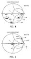
- FIG. 4 is an impedance chart illustrating the load impedance seen from the reference plane P2 shown in FIG. 1 .
- FIG. 5 is an impedance chart illustrating the load impedance seen from the reference plane P3 shown in FIG. 1 .
- FIG. 6 is an impedance chart illustrating the load impedance seen from the reference plane P4 shown in FIG. 1 .
- FIG. 7 is an impedance chart illustrating the load impedance seen from the reference plane P5 shown in FIG. 1 .
- the impedance charts of FIGS. 4 to 7 are normalized so that the center point O represents 1 ⁇ .
- the symbols m11-m15 represent the load impedance at the fundamental frequency f1.
- the symbols m21-m25 represent the load impedance at the second harmonic frequency f2.
- the symbols m31-m35 represent the load impedance at the third harmonic frequency f3.
- This example shows the case where the load impedance m15 at the fundamental frequency f1 seen from the reference plane P5 is transformed to approximately (1+j1) ⁇ .
- the side of the output terminal 18 connected with the external load Zo is seen from the reference plane P0. Then, the load impedance m10 at the fundamental frequency f1, the load impedance m20 at the second harmonic frequency f2, and the load impedance m30 at the third harmonic frequency f3 are located at the center point O near 50 ⁇ .
- the load impedance at the fundamental, second harmonic, and third harmonic frequencies can be determined by measurement and simulation, and indicated on the impedance chart.
- the electrical length of the microstrip line 111 at the fundamental frequency f1 is 96 degrees.
- the electrical length of 96 degrees corresponds to approximately a quarter wavelength.
- the microstrip line 111 operates like a quarter wavelength transformer.
- the characteristic impedance Zc11 of the microstrip line 111 is lower than the load impedance m0 of the external load Zo.
- the load impedance m0 is e.g. 50 ⁇ .
- the load impedance m11 at the fundamental frequency f1 seen from the reference plane P1 is transformed to an impedance lower than the load impedance m0 of the external load Zo.
- the load impedance in the first frequency band Bw1 is transformed to a neighborhood portion including the load impedance m11. This portion is indicated as portion 3A in FIGS. 3A and 3B .
- the electrical length EL11 of the microstrip line 111 is approximately a three-quarter wavelength at the third harmonic frequency f3.
- the load impedance m31 at the third harmonic frequency f3 is transformed to the portion 3A.
- the signal having a frequency of three times that of the fundamental signal S1 is referred to as third harmonic signal S3.
- the load impedance of the third harmonic signal S3 having a frequency band is also transformed to the portion 3A.
- the electrical length EL11 of the microstrip line 111 is approximately a two-quarter wavelength at the second harmonic frequency f2.
- the load impedance m21 at the second harmonic frequency f2 remains near 50 ⁇ without substantial change.
- This portion near 50 ⁇ is indicated as portion 3B in FIGS. 3A and 3B .
- the load impedance m21 of the second harmonic is separated from the load impedance m11 for the fundamental and the load impedance m31 for the third harmonic.
- the characteristic impedance Zc12 of the microstrip line 112 is lower than the characteristic impedance Zc11 of the microstrip line 111.
- the electrical length EL12 of the microstrip line 112 at the fundamental frequency f1 is as short as 26 degrees.
- the load impedance m22 at the second harmonic frequency f2 is transformed to a portion 4B different from the portion 4A.
- the electrical length at the fundamental frequency f1 is as short as 26 degrees.
- the electrical length is less than or equal to a three-quarter wavelength also at the third harmonic frequency f3.
- the load impedance m32 at the third harmonic frequency f3 is transformed to a portion 4C different from the portion 4A and the portion 4B. That is, the load impedances m12, m22, and m32 at the fundamental, second harmonic, and third harmonic frequencies are separated.
- the characteristic impedance Zc13 of the microstrip line 113 is higher than that of the microstrip line 112.
- the electrical length EL13 at the fundamental frequency f1 is 24 degrees.
- the microstrip line 113 is added to the microstrip line 112.
- the load impedance m13 at the fundamental frequency f1 seen from the reference plane P3 is transformed to a portion 5A near 1 ⁇ .
- the load impedance m23 at the second harmonic frequency f2 is transformed to a portion 5B.
- the portion 5B is an inductive region near ⁇ ⁇ .
- the load impedance m33 at the third harmonic frequency f3 is transformed to a portion 5C.
- the portion 5C is inductive near ⁇ ⁇ and different from the portion 5B.
- an inductive impedance is indicated in the upper half region of the impedance chart.
- a capacitive impedance is indicated in the lower half region of the impedance chart.
- the characteristic impedance Zc14 of the microstrip line 114 is close to the load impedance m13 at the fundamental frequency f1 seen from the reference plane P3.
- the microstrip line 114 is added to the microstrip line 113.
- the load impedance m14 at the fundamental frequency f1 seen from the reference plane P4 remains near 1 ⁇ without substantial change.
- This portion near 1 ⁇ is indicated as portion 6A in FIG. 6 .
- the load impedance m24 at the second harmonic frequency f2 is transformed to a portion 6B.
- the portion 6B is an inductive region near ⁇ ⁇ .
- the load impedance m34 at the third harmonic frequency f3 is transformed to a portion 6C.
- the portion 6C is a capacitive region. At this stage, the load impedance m34 for the third harmonic is capacitive.
- the wire part 115 is added to the microstrip line 114.
- the load impedance m15 at the fundamental frequency f1 seen from the reference plane P5 is transformed to a portion 7A near (1+j1) ⁇ because of the added inductivity of the wire part 115.
- the load impedance m25 at the second harmonic frequency f2 remains near ⁇ ⁇ .
- This portion near ⁇ ⁇ is indicated as portion 7B in FIG. 7 .
- the load impedance m35 at the third harmonic frequency f3 is transformed to a portion 7C near 0 ⁇ due to resonance between the capacitivity in the aforementioned portion 6C and the inductivity of the wire part 115.
- the amount of capacitivity produced by the addition of the microstrip line 114 may be smaller than the amount of inductivity of the wire part 115.
- the load impedance m35 at the third harmonic frequency f3 is not transformed to approximately 0 ⁇ due to insufficient resonance between capacitivity and inductivity.
- the amount of capacitivity produced by the addition of the microstrip line 114 may be larger than the amount of inductivity of the wire part 115.
- the load impedance m35 at the third harmonic frequency f3 is not transformed to approximately 0 ⁇ due to insufficient resonance between capacitivity and inductivity.
- the electrical length EL14 of the microstrip line 114 needs to be selected so as to achieve resonance between the capacitivity produced by the addition of the microstrip line 114 and the inductivity of the wire part 115.
- the high-frequency semiconductor amplifier 1 has been described with reference to the example in which the load impedance at the fundamental frequency f1 seen from the reference plane P5 is transformed to approximately (1+j1) ⁇ .
- this embodiment is not limited thereto.
- the load impedance may be transformed to a different desired load impedance.
- High power-added efficiency is achieved in the high-frequency semiconductor amplifier by an output matching circuit connected to the output of the high-frequency semiconductor amplifying element.
- the load impedance at the fundamental frequency is matched with a desired impedance.
- the impedance at even harmonics such as the second harmonic frequency is set to ⁇ ⁇ .
- the impedance at odd harmonics such as the third harmonic frequency is set to 0 ⁇ .
- Such operation of the high-frequency semiconductor amplifier is referred to as inverse class-F operation.
- the inverse class-F operation of the high-frequency semiconductor amplifier eliminates the even harmonics of voltage and the odd harmonics of current. The voltage and the current both exist only at the fundamental frequency. This realizes high power-added efficiency.
- the load impedance m12 at the fundamental frequency f1 is transformed to the portion 4A shown in FIG. 4 .
- the load impedance m22 at the second harmonic frequency f2 is transformed to the portion 4B shown in FIG. 4 .
- the load impedance m32 at the third harmonic frequency f3 is transformed to the portion 4C shown in FIG. 4 .
- the portions 4A, 4B, and 4C are separate.
- the load impedance m15 at the fundamental frequency f1 seen from the reference plane P5 is easily transformed to the final target of approximately (1+j1) ⁇ .
- the load impedance m25 at the second harmonic frequency f2 is easily transformed to the final target of approximately ⁇ ⁇ .
- the load impedance m35 at the third harmonic frequency f3 is easily transformed to the final target of approximately 0 ⁇ .
- the load impedance m14 at the fundamental frequency f1 remains near 1 ⁇ .
- the load impedance m24 at the second harmonic frequency f2 is transformed to approximately ⁇ ⁇ .
- the load impedance m34 at the third harmonic frequency f3 is transformed to a capacitive region.
- the load impedance m15 at the fundamental frequency f1 is transformed to approximately (1+j1) ⁇ .
- the load impedance m25 at the second harmonic frequency f2 is transformed to approximately ⁇ ⁇ .
- the load impedance m35 at the third harmonic frequency f3 is resonated with the inductivity of the wire part 115 and transformed to approximately 0 ⁇ .
- high power-added efficiency can be achieved by the inverse class-F operation of the high-frequency semiconductor amplifier 1.
- the power-added efficiency can be improved by approximately 5-10%.
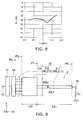
- FIG. 8 is a graph illustrating the return loss RL seen from the reference plane P5 shown in FIG. 1 .
- the horizontal axis represents frequency (GHz).
- the vertical axis represents the return loss RL (dB) for the load impedance m15 provided to the high-frequency semiconductor amplifying element 14.
- the load impedance m15 is e.g. (1+j1) ⁇ .
- the return loss RL for the fundamental can be set to 30 dB or more at frequency f of approximately 2.7-3.1 GHz.
- FIG. 9 is a schematic view showing the configuration of a high-frequency semiconductor amplifier according to this comparative example.
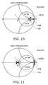
- FIG. 10 is an impedance chart illustrating the load impedance seen from the reference plane P1 shown in FIG. 9 .
- FIG. 11 is an impedance chart illustrating the load impedance seen from the reference plane P2 shown in FIG. 9 .
- FIG. 12 is an impedance chart illustrating the load impedance seen from the reference plane P5 shown in FIG. 9 .
- the impedance charts of FIGS. 10 to 12 are normalized so that the center point O represents 1 ⁇ .
- TABLE 2 is a table illustrating the electrical characteristics and dimensions of the microstrip lines in the first comparative example according to this embodiment.
- the output matching circuit 22 in this comparative example is formed from a microstrip line 211 (ML211), a microstrip line 212 (ML212), and a wire part 115.
- the position of the reference plane P0 is similar to the position in the above first embodiment.
- the load impedance m10 at the fundamental frequency f1 seen from the reference plane P0 is similar to that of the above first embodiment (see FIG. 2 ).
- the load impedance m20 at the second harmonic frequency f2 is also similar to that of the above first embodiment (see FIG. 2 ).
- the load impedance m30 at the third harmonic frequency f3 is also similar to that of the above first embodiment (see FIG. 2 ).
- the characteristic impedance Zc21 of the microstrip line 211 (ML211) is 18.8 ⁇ .
- the electrical length EL21 at the fundamental frequency f1 is 90 degrees.
- the relative permittivity ⁇ r21 is 10.
- the thickness t21 is 150 ⁇ m.
- the line width W21 is 0.68 mm.
- the line length L21 is 8.83 mm.
- the characteristic impedance Zc22 of the microstrip line 212 (ML212) is 2.66 ⁇ .
- the electrical length EL22 at the fundamental frequency f1 is 90 degrees.
- the relative permittivity ⁇ r22 is 40.
- the thickness t22 is 250 ⁇ m.
- the line width W22 is 5.06 mm.
- the line length L22 is 4.14 mm.
- the load impedance m11a at the fundamental frequency f1 and the load impedance m31a at the third harmonic frequency f3 seen from the reference plane P1 are transformed to a portion 10A having an impedance higher than 1 ⁇ and lower than 50 ⁇ .
- the electrical length EL21 of the microstrip line 211 is approximately a two-quarter wavelength at the second harmonic frequency f2.
- the load impedance m21a at the second harmonic frequency f2 remains near 50 ⁇ . This portion near 50 ⁇ is indicated as portion 10B in FIG. 10 .
- the load impedance m12a at the fundamental frequency f1 and the load impedance m32a at the third harmonic frequency f3 seen from the reference plane P2 are transformed to a portion 11A having an impedance of approximately 1 ⁇ .
- the electrical length EL22 of the microstrip line 212 is approximately a two-quarter wavelength at the second harmonic.
- the load impedance m22a at the second harmonic frequency f2 remains near 50 ⁇ . This portion near 50 ⁇ is indicated as portion 11B in FIG. 11 .
- the inductivity of the wire part 115 is added by the wire part 115.
- the load impedance m15a at the fundamental frequency f1 seen from the reference plane P5 is transformed to a portion 12A near (1+j1) ⁇ .
- the load impedance m25a at the second harmonic frequency f2 is transformed to a portion 12B near ⁇ ⁇ .
- the load impedance m35a at the third harmonic frequency f3 is transformed to a portion 12C.
- the load impedance m25a at the second harmonic frequency f2 is set to approximately ⁇ ⁇ , but the load impedance m35a at the third harmonic frequency f3 is not set to approximately 0 ⁇ .
- the high-frequency semiconductor amplifier 2 does not perform the inverse class-F operation.
- FIG. 13 is a schematic view showing the configuration of a high-frequency semiconductor amplifier according to the second comparative example of the first embodiment.
- FIG. 14 is an impedance chart illustrating the load impedance seen from the reference plane P3 shown in FIG. 13 .
- FIG. 15 is an impedance chart illustrating the load impedance seen from the reference plane P5 shown in FIG. 13 .
- the impedance charts of FIGS. 14 and 15 are normalized so that the center point O represents 1 ⁇ .
- TABLE 3 is a table illustrating the electrical characteristics and dimensions of the microstrip lines in the second comparative example according to this embodiment.
- the output matching circuit 23 in the second comparative example of this embodiment is different from the output matching circuit 22 in the above first comparative example in that the microstrip line 313 (ML313) is provided between the microstrip line 212 and the wire part 115.
- the load impedances m10, m11, and m12 at the fundamental frequency f1 seen from the reference planes P0, P1, and P2 are similar to those of the above first comparative example.
- the load impedances m20, m21, and m22 at the second harmonic frequency f2 seen from the reference planes P0, P1, and P2 are similar to those of the above first comparative example.
- the load impedances m30, m31, and m32 at the third harmonic frequency f3 seen from the reference planes P0, P1, and P2 are similar to those of the above first comparative example.
- the characteristic impedance Zc33 of the microstrip line 313 (ML313) is 1.0 ⁇ .
- the electrical length EL33 at the fundamental frequency f1 is 90 degrees.
- the relative permittivity ⁇ r33 is 90.
- the thickness t33 is 135 ⁇ m.
- the line width W33 is 5.05 mm.
- the line length L33 is 2.71 mm.
- the characteristic impedance Zc33 of the microstrip line 313 is close to the load impedance m12a (see FIG. 11 ) at the fundamental frequency f1 seen from the reference plane P2.
- the microstrip line 313 is added to the microstrip line 212.
- the load impedance m13b at the fundamental frequency f1 seen from the reference plane P3 remains near 1 ⁇ as in the case seen from the reference plane P2.
- the load impedance m33b at the third harmonic frequency f3 also remains near 1 ⁇ . This portion near 1 ⁇ is indicated as portion 14A.
- the load impedance m23b at the second harmonic frequency f2 is transformed to a portion 14B near ⁇ ⁇ .
- the inductivity of the wire part 115 is added by the wire part 115.
- the load impedance m15b at the fundamental frequency f1 seen from the reference plane P5 is transformed to a portion 15A near (1+j1) ⁇ .
- the addition of the wire part 115 only results in increasing the impedance.
- the load impedance m25b at the second harmonic frequency f2 remains near ⁇ ⁇ without substantial change.
- This portion near ⁇ ⁇ is indicated as portion 15B in FIG. 15 .
- the load impedance m35b at the third harmonic frequency f3 is transformed to a portion 15C because of the added inductivity of the wire part 115.
- the load impedance m35b at the third harmonic frequency f3 is not set to approximately 0 ⁇ .
- the high-frequency semiconductor amplifier 3 does not perform the inverse class-F operation.
- the embodiment described above can provide a high-frequency semiconductor amplifier for amplifying high-frequency signals at high power-added efficiency.
Landscapes
- Engineering & Computer Science (AREA)
- Power Engineering (AREA)
- Microwave Amplifiers (AREA)
- Amplifiers (AREA)
Applications Claiming Priority (1)
| Application Number | Priority Date | Filing Date | Title |
|---|---|---|---|
| JP2015013501A JP6189880B2 (ja) | 2015-01-27 | 2015-01-27 | 高周波半導体増幅器 |
Publications (2)
| Publication Number | Publication Date |
|---|---|
| EP3051694A1 true EP3051694A1 (de) | 2016-08-03 |
| EP3051694B1 EP3051694B1 (de) | 2019-07-24 |
Family
ID=55236273
Family Applications (1)
| Application Number | Title | Priority Date | Filing Date |
|---|---|---|---|
| EP16152706.4A Active EP3051694B1 (de) | 2015-01-27 | 2016-01-26 | Hochfrequenz-halbleiterverstärker |
Country Status (3)
| Country | Link |
|---|---|
| US (1) | US9985584B2 (de) |
| EP (1) | EP3051694B1 (de) |
| JP (1) | JP6189880B2 (de) |
Families Citing this family (1)
| Publication number | Priority date | Publication date | Assignee | Title |
|---|---|---|---|---|
| JP6049673B2 (ja) | 2014-10-31 | 2016-12-21 | 株式会社東芝 | 半導体増幅装置 |
Citations (3)
| Publication number | Priority date | Publication date | Assignee | Title |
|---|---|---|---|---|
| JP2009207060A (ja) * | 2008-02-29 | 2009-09-10 | Mitsubishi Electric Corp | 高周波半導体増幅器 |
| US20130234794A1 (en) * | 2012-03-08 | 2013-09-12 | Kazutaka Takagi | Microwave semiconductor amplifier |
| US20140218105A1 (en) * | 2013-02-01 | 2014-08-07 | Fujitsu Limited | Amplifier and amplifying method |
Family Cites Families (25)
| Publication number | Priority date | Publication date | Assignee | Title |
|---|---|---|---|---|
| JPH0738548B2 (ja) * | 1993-01-07 | 1995-04-26 | 日本電気株式会社 | 電力整合回路 |
| JP2513146B2 (ja) | 1993-09-20 | 1996-07-03 | 日本電気株式会社 | 高効率増幅回路 |
| JP2001111362A (ja) | 1999-10-06 | 2001-04-20 | Nec Corp | 高調波処理回路及びそれを用いた高電力効率増幅回路 |
| US6744409B2 (en) * | 2001-12-28 | 2004-06-01 | National University Of Singapore | High efficiency transmit antenna |
| JP4520204B2 (ja) * | 2004-04-14 | 2010-08-04 | 三菱電機株式会社 | 高周波電力増幅器 |
| US8164396B2 (en) * | 2006-08-08 | 2012-04-24 | National University Corporation, The University Of Electro-Communications | Harmonic processing circuit and amplifying circuit using the same |
| KR100814415B1 (ko) * | 2007-02-14 | 2008-03-18 | 포항공과대학교 산학협력단 | 하모닉 제어 회로를 이용한 고효율 도허티 전력 증폭기 |
| KR101399053B1 (ko) * | 2007-06-05 | 2014-05-28 | 포항공과대학교 산학협력단 | 신호 크기 정보 제거와 복원 기술을 사용한 전력송신기에서의 전력 증폭을 위한 장치 및 방법 |
| JP2009081605A (ja) * | 2007-09-26 | 2009-04-16 | Univ Of Electro-Communications | 逆f級増幅回路 |
| JP2009130472A (ja) * | 2007-11-20 | 2009-06-11 | Univ Of Electro-Communications | 逆f級増幅回路 |
| JP5083201B2 (ja) | 2008-12-25 | 2012-11-28 | 三菱電機株式会社 | 高周波半導体増幅器 |
| EP2262107B1 (de) * | 2009-06-10 | 2012-09-12 | Alcatel Lucent | Verstärker im Inversen F-Betrieb und Verfahren |
| JP5408616B2 (ja) * | 2009-08-31 | 2014-02-05 | 国立大学法人電気通信大学 | 増幅回路 |
| JP5424790B2 (ja) * | 2009-09-18 | 2014-02-26 | 三菱電機株式会社 | 高出力増幅器 |
| WO2012040879A1 (en) * | 2010-09-30 | 2012-04-05 | Telefonaktiebolaget Lm Ericsson (Publ) | Multi-band switched-mode power amplifier |
| CN103765765B (zh) * | 2011-08-29 | 2017-02-15 | 国立大学法人电气通信大学 | 高效率功率放大器 |
| JP2013055405A (ja) * | 2011-09-01 | 2013-03-21 | Nec Corp | F級増幅回路及びこれを用いた送信装置 |
| JP5468095B2 (ja) | 2012-03-08 | 2014-04-09 | 株式会社東芝 | 高周波半導体増幅器 |
| JP5619055B2 (ja) | 2012-03-08 | 2014-11-05 | 株式会社東芝 | 高周波半導体増幅器 |
| JP5603893B2 (ja) * | 2012-03-08 | 2014-10-08 | 株式会社東芝 | 高周波半導体増幅器 |
| JP2015149627A (ja) | 2014-02-06 | 2015-08-20 | 株式会社東芝 | 高周波半導体増幅器 |
| JP2015149626A (ja) | 2014-02-06 | 2015-08-20 | 株式会社東芝 | 高周波半導体増幅器 |
| US9641140B2 (en) * | 2014-06-27 | 2017-05-02 | Nxp Usa, Inc. | Method and apparatus for a multi-harmonic matching network |
| CN204119176U (zh) * | 2014-10-24 | 2015-01-21 | 天津大学 | 一种高效率f类/逆f类功率放大器 |
| JP6648979B2 (ja) | 2015-04-06 | 2020-02-19 | 株式会社東芝 | 半導体増幅装置 |
-
2015
- 2015-01-27 JP JP2015013501A patent/JP6189880B2/ja active Active
-
2016
- 2016-01-26 EP EP16152706.4A patent/EP3051694B1/de active Active
- 2016-01-27 US US15/007,945 patent/US9985584B2/en active Active
Patent Citations (3)
| Publication number | Priority date | Publication date | Assignee | Title |
|---|---|---|---|---|
| JP2009207060A (ja) * | 2008-02-29 | 2009-09-10 | Mitsubishi Electric Corp | 高周波半導体増幅器 |
| US20130234794A1 (en) * | 2012-03-08 | 2013-09-12 | Kazutaka Takagi | Microwave semiconductor amplifier |
| US20140218105A1 (en) * | 2013-02-01 | 2014-08-07 | Fujitsu Limited | Amplifier and amplifying method |
Also Published As
| Publication number | Publication date |
|---|---|
| US20160218676A1 (en) | 2016-07-28 |
| JP2016139922A (ja) | 2016-08-04 |
| EP3051694B1 (de) | 2019-07-24 |
| US9985584B2 (en) | 2018-05-29 |
| JP6189880B2 (ja) | 2017-08-30 |
Similar Documents
| Publication | Publication Date | Title |
|---|---|---|
| JP5603893B2 (ja) | 高周波半導体増幅器 | |
| US10403976B2 (en) | Antenna and wireless communication apparatus | |
| JP5619055B2 (ja) | 高周波半導体増幅器 | |
| US20140015721A1 (en) | Antenna apparatus | |
| US9035702B2 (en) | Microwave semiconductor amplifier | |
| EP3051695B1 (de) | Hochfrequenz-halbleiterverstärker | |
| US11296662B2 (en) | High-frequency power amplifier | |
| JP2002335136A (ja) | 高周波半導体装置 | |
| ITMI20121238A1 (it) | Dispositivo trasformatore balun planare | |
| JP5468095B2 (ja) | 高周波半導体増幅器 | |
| EP3051693B1 (de) | Hochfrequenz-halbleiterverstärker | |
| CN107611618A (zh) | 裂缝天线 | |
| TWI629836B (zh) | 雙頻偶極天線與電子系統 | |
| EP3051694B1 (de) | Hochfrequenz-halbleiterverstärker | |
| JP2016092527A (ja) | 半導体増幅器用バイアス回路および半導体増幅装置 | |
| KR102564085B1 (ko) | 도허티 증폭기 | |
| JP6431002B2 (ja) | 電力伝送通信ユニット及び電力伝送通信装置 | |
| CN113366760B (zh) | 谐波处理电路和放大器 | |
| CN110168931B (zh) | 功率放大器 | |
| JP6523108B2 (ja) | 高周波半導体増幅器 | |
| US9577578B2 (en) | Amplifying device and radio communication device | |
| EP3155720B1 (de) | Breitbandiger impedanzwandler | |
| CN103298166B (zh) | 基于超材料天线的移动通信基站 | |
| WO2010140406A1 (ja) | アンテナ装置及び無線通信機 | |
| JP2013219484A (ja) | 高周波半導体増幅器 |
Legal Events
| Date | Code | Title | Description |
|---|---|---|---|
| PUAI | Public reference made under article 153(3) epc to a published international application that has entered the european phase |
Free format text: ORIGINAL CODE: 0009012 |
|
| 17P | Request for examination filed |
Effective date: 20160126 |
|
| AK | Designated contracting states |
Kind code of ref document: A1 Designated state(s): AL AT BE BG CH CY CZ DE DK EE ES FI FR GB GR HR HU IE IS IT LI LT LU LV MC MK MT NL NO PL PT RO RS SE SI SK SM TR |
|
| AX | Request for extension of the european patent |
Extension state: BA ME |
|
| STAA | Information on the status of an ep patent application or granted ep patent |
Free format text: STATUS: EXAMINATION IS IN PROGRESS |
|
| 17Q | First examination report despatched |
Effective date: 20170926 |
|
| REG | Reference to a national code |
Ref country code: DE Ref legal event code: R079 Ref document number: 602016017157 Country of ref document: DE Free format text: PREVIOUS MAIN CLASS: H03F0003217000 Ipc: H01P0001240000 |
|
| RIC1 | Information provided on ipc code assigned before grant |
Ipc: H01L 23/66 20060101ALI20190213BHEP Ipc: H01P 5/02 20060101ALI20190213BHEP Ipc: H03F 1/02 20060101ALI20190213BHEP Ipc: H01P 1/28 20060101ALI20190213BHEP Ipc: H01P 1/24 20060101AFI20190213BHEP Ipc: H03F 3/19 20060101ALI20190213BHEP Ipc: H03F 3/60 20060101ALI20190213BHEP Ipc: H03F 1/56 20060101ALI20190213BHEP Ipc: H03F 3/217 20060101ALI20190213BHEP |
|
| GRAP | Despatch of communication of intention to grant a patent |
Free format text: ORIGINAL CODE: EPIDOSNIGR1 |
|
| STAA | Information on the status of an ep patent application or granted ep patent |
Free format text: STATUS: GRANT OF PATENT IS INTENDED |
|
| INTG | Intention to grant announced |
Effective date: 20190329 |
|
| GRAS | Grant fee paid |
Free format text: ORIGINAL CODE: EPIDOSNIGR3 |
|
| GRAA | (expected) grant |
Free format text: ORIGINAL CODE: 0009210 |
|
| STAA | Information on the status of an ep patent application or granted ep patent |
Free format text: STATUS: THE PATENT HAS BEEN GRANTED |
|
| AK | Designated contracting states |
Kind code of ref document: B1 Designated state(s): AL AT BE BG CH CY CZ DE DK EE ES FI FR GB GR HR HU IE IS IT LI LT LU LV MC MK MT NL NO PL PT RO RS SE SI SK SM TR |
|
| REG | Reference to a national code |
Ref country code: GB Ref legal event code: FG4D |
|
| REG | Reference to a national code |
Ref country code: CH Ref legal event code: EP |
|
| REG | Reference to a national code |
Ref country code: DE Ref legal event code: R096 Ref document number: 602016017157 Country of ref document: DE |
|
| REG | Reference to a national code |
Ref country code: AT Ref legal event code: REF Ref document number: 1159301 Country of ref document: AT Kind code of ref document: T Effective date: 20190815 |
|
| REG | Reference to a national code |
Ref country code: IE Ref legal event code: FG4D |
|
| REG | Reference to a national code |
Ref country code: NL Ref legal event code: MP Effective date: 20190724 |
|
| REG | Reference to a national code |
Ref country code: LT Ref legal event code: MG4D |
|
| REG | Reference to a national code |
Ref country code: AT Ref legal event code: MK05 Ref document number: 1159301 Country of ref document: AT Kind code of ref document: T Effective date: 20190724 |
|
| PG25 | Lapsed in a contracting state [announced via postgrant information from national office to epo] |
Ref country code: NL Free format text: LAPSE BECAUSE OF FAILURE TO SUBMIT A TRANSLATION OF THE DESCRIPTION OR TO PAY THE FEE WITHIN THE PRESCRIBED TIME-LIMIT Effective date: 20190724 Ref country code: PT Free format text: LAPSE BECAUSE OF FAILURE TO SUBMIT A TRANSLATION OF THE DESCRIPTION OR TO PAY THE FEE WITHIN THE PRESCRIBED TIME-LIMIT Effective date: 20191125 Ref country code: SE Free format text: LAPSE BECAUSE OF FAILURE TO SUBMIT A TRANSLATION OF THE DESCRIPTION OR TO PAY THE FEE WITHIN THE PRESCRIBED TIME-LIMIT Effective date: 20190724 Ref country code: NO Free format text: LAPSE BECAUSE OF FAILURE TO SUBMIT A TRANSLATION OF THE DESCRIPTION OR TO PAY THE FEE WITHIN THE PRESCRIBED TIME-LIMIT Effective date: 20191024 Ref country code: HR Free format text: LAPSE BECAUSE OF FAILURE TO SUBMIT A TRANSLATION OF THE DESCRIPTION OR TO PAY THE FEE WITHIN THE PRESCRIBED TIME-LIMIT Effective date: 20190724 Ref country code: AT Free format text: LAPSE BECAUSE OF FAILURE TO SUBMIT A TRANSLATION OF THE DESCRIPTION OR TO PAY THE FEE WITHIN THE PRESCRIBED TIME-LIMIT Effective date: 20190724 Ref country code: LT Free format text: LAPSE BECAUSE OF FAILURE TO SUBMIT A TRANSLATION OF THE DESCRIPTION OR TO PAY THE FEE WITHIN THE PRESCRIBED TIME-LIMIT Effective date: 20190724 Ref country code: BG Free format text: LAPSE BECAUSE OF FAILURE TO SUBMIT A TRANSLATION OF THE DESCRIPTION OR TO PAY THE FEE WITHIN THE PRESCRIBED TIME-LIMIT Effective date: 20191024 Ref country code: FI Free format text: LAPSE BECAUSE OF FAILURE TO SUBMIT A TRANSLATION OF THE DESCRIPTION OR TO PAY THE FEE WITHIN THE PRESCRIBED TIME-LIMIT Effective date: 20190724 |
|
| PG25 | Lapsed in a contracting state [announced via postgrant information from national office to epo] |
Ref country code: IS Free format text: LAPSE BECAUSE OF FAILURE TO SUBMIT A TRANSLATION OF THE DESCRIPTION OR TO PAY THE FEE WITHIN THE PRESCRIBED TIME-LIMIT Effective date: 20191124 Ref country code: GR Free format text: LAPSE BECAUSE OF FAILURE TO SUBMIT A TRANSLATION OF THE DESCRIPTION OR TO PAY THE FEE WITHIN THE PRESCRIBED TIME-LIMIT Effective date: 20191025 Ref country code: ES Free format text: LAPSE BECAUSE OF FAILURE TO SUBMIT A TRANSLATION OF THE DESCRIPTION OR TO PAY THE FEE WITHIN THE PRESCRIBED TIME-LIMIT Effective date: 20190724 Ref country code: RS Free format text: LAPSE BECAUSE OF FAILURE TO SUBMIT A TRANSLATION OF THE DESCRIPTION OR TO PAY THE FEE WITHIN THE PRESCRIBED TIME-LIMIT Effective date: 20190724 Ref country code: AL Free format text: LAPSE BECAUSE OF FAILURE TO SUBMIT A TRANSLATION OF THE DESCRIPTION OR TO PAY THE FEE WITHIN THE PRESCRIBED TIME-LIMIT Effective date: 20190724 Ref country code: LV Free format text: LAPSE BECAUSE OF FAILURE TO SUBMIT A TRANSLATION OF THE DESCRIPTION OR TO PAY THE FEE WITHIN THE PRESCRIBED TIME-LIMIT Effective date: 20190724 |
|
| PG25 | Lapsed in a contracting state [announced via postgrant information from national office to epo] |
Ref country code: TR Free format text: LAPSE BECAUSE OF FAILURE TO SUBMIT A TRANSLATION OF THE DESCRIPTION OR TO PAY THE FEE WITHIN THE PRESCRIBED TIME-LIMIT Effective date: 20190724 |
|
| PG25 | Lapsed in a contracting state [announced via postgrant information from national office to epo] |
Ref country code: EE Free format text: LAPSE BECAUSE OF FAILURE TO SUBMIT A TRANSLATION OF THE DESCRIPTION OR TO PAY THE FEE WITHIN THE PRESCRIBED TIME-LIMIT Effective date: 20190724 Ref country code: DK Free format text: LAPSE BECAUSE OF FAILURE TO SUBMIT A TRANSLATION OF THE DESCRIPTION OR TO PAY THE FEE WITHIN THE PRESCRIBED TIME-LIMIT Effective date: 20190724 Ref country code: IT Free format text: LAPSE BECAUSE OF FAILURE TO SUBMIT A TRANSLATION OF THE DESCRIPTION OR TO PAY THE FEE WITHIN THE PRESCRIBED TIME-LIMIT Effective date: 20190724 Ref country code: RO Free format text: LAPSE BECAUSE OF FAILURE TO SUBMIT A TRANSLATION OF THE DESCRIPTION OR TO PAY THE FEE WITHIN THE PRESCRIBED TIME-LIMIT Effective date: 20190724 Ref country code: PL Free format text: LAPSE BECAUSE OF FAILURE TO SUBMIT A TRANSLATION OF THE DESCRIPTION OR TO PAY THE FEE WITHIN THE PRESCRIBED TIME-LIMIT Effective date: 20190724 |
|
| PG25 | Lapsed in a contracting state [announced via postgrant information from national office to epo] |
Ref country code: IS Free format text: LAPSE BECAUSE OF FAILURE TO SUBMIT A TRANSLATION OF THE DESCRIPTION OR TO PAY THE FEE WITHIN THE PRESCRIBED TIME-LIMIT Effective date: 20200224 Ref country code: SK Free format text: LAPSE BECAUSE OF FAILURE TO SUBMIT A TRANSLATION OF THE DESCRIPTION OR TO PAY THE FEE WITHIN THE PRESCRIBED TIME-LIMIT Effective date: 20190724 Ref country code: CZ Free format text: LAPSE BECAUSE OF FAILURE TO SUBMIT A TRANSLATION OF THE DESCRIPTION OR TO PAY THE FEE WITHIN THE PRESCRIBED TIME-LIMIT Effective date: 20190724 Ref country code: SM Free format text: LAPSE BECAUSE OF FAILURE TO SUBMIT A TRANSLATION OF THE DESCRIPTION OR TO PAY THE FEE WITHIN THE PRESCRIBED TIME-LIMIT Effective date: 20190724 |
|
| REG | Reference to a national code |
Ref country code: DE Ref legal event code: R097 Ref document number: 602016017157 Country of ref document: DE |
|
| PLBE | No opposition filed within time limit |
Free format text: ORIGINAL CODE: 0009261 |
|
| STAA | Information on the status of an ep patent application or granted ep patent |
Free format text: STATUS: NO OPPOSITION FILED WITHIN TIME LIMIT |
|
| PG2D | Information on lapse in contracting state deleted |
Ref country code: IS |
|
| 26N | No opposition filed |
Effective date: 20200603 |
|
| PG25 | Lapsed in a contracting state [announced via postgrant information from national office to epo] |
Ref country code: SI Free format text: LAPSE BECAUSE OF FAILURE TO SUBMIT A TRANSLATION OF THE DESCRIPTION OR TO PAY THE FEE WITHIN THE PRESCRIBED TIME-LIMIT Effective date: 20190724 Ref country code: MC Free format text: LAPSE BECAUSE OF FAILURE TO SUBMIT A TRANSLATION OF THE DESCRIPTION OR TO PAY THE FEE WITHIN THE PRESCRIBED TIME-LIMIT Effective date: 20190724 |
|
| REG | Reference to a national code |
Ref country code: CH Ref legal event code: PL |
|
| GBPC | Gb: european patent ceased through non-payment of renewal fee |
Effective date: 20200126 |
|
| REG | Reference to a national code |
Ref country code: BE Ref legal event code: MM Effective date: 20200131 |
|
| PG25 | Lapsed in a contracting state [announced via postgrant information from national office to epo] |
Ref country code: LU Free format text: LAPSE BECAUSE OF NON-PAYMENT OF DUE FEES Effective date: 20200126 Ref country code: GB Free format text: LAPSE BECAUSE OF NON-PAYMENT OF DUE FEES Effective date: 20200126 |
|
| PG25 | Lapsed in a contracting state [announced via postgrant information from national office to epo] |
Ref country code: LI Free format text: LAPSE BECAUSE OF NON-PAYMENT OF DUE FEES Effective date: 20200131 Ref country code: BE Free format text: LAPSE BECAUSE OF NON-PAYMENT OF DUE FEES Effective date: 20200131 Ref country code: CH Free format text: LAPSE BECAUSE OF NON-PAYMENT OF DUE FEES Effective date: 20200131 |
|
| PG25 | Lapsed in a contracting state [announced via postgrant information from national office to epo] |
Ref country code: IE Free format text: LAPSE BECAUSE OF NON-PAYMENT OF DUE FEES Effective date: 20200126 |
|
| PG25 | Lapsed in a contracting state [announced via postgrant information from national office to epo] |
Ref country code: MT Free format text: LAPSE BECAUSE OF FAILURE TO SUBMIT A TRANSLATION OF THE DESCRIPTION OR TO PAY THE FEE WITHIN THE PRESCRIBED TIME-LIMIT Effective date: 20190724 Ref country code: CY Free format text: LAPSE BECAUSE OF FAILURE TO SUBMIT A TRANSLATION OF THE DESCRIPTION OR TO PAY THE FEE WITHIN THE PRESCRIBED TIME-LIMIT Effective date: 20190724 |
|
| PG25 | Lapsed in a contracting state [announced via postgrant information from national office to epo] |
Ref country code: MK Free format text: LAPSE BECAUSE OF FAILURE TO SUBMIT A TRANSLATION OF THE DESCRIPTION OR TO PAY THE FEE WITHIN THE PRESCRIBED TIME-LIMIT Effective date: 20190724 |
|
| PGFP | Annual fee paid to national office [announced via postgrant information from national office to epo] |
Ref country code: FR Payment date: 20251128 Year of fee payment: 11 |
|
| PGFP | Annual fee paid to national office [announced via postgrant information from national office to epo] |
Ref country code: DE Payment date: 20251203 Year of fee payment: 11 |