EP3040397B1 - Ätzlösungen und verfahren zur verwendung davon - Google Patents
Ätzlösungen und verfahren zur verwendung davon Download PDFInfo
- Publication number
- EP3040397B1 EP3040397B1 EP15202875.9A EP15202875A EP3040397B1 EP 3040397 B1 EP3040397 B1 EP 3040397B1 EP 15202875 A EP15202875 A EP 15202875A EP 3040397 B1 EP3040397 B1 EP 3040397B1
- Authority
- EP
- European Patent Office
- Prior art keywords
- composition
- acid
- hydroxide
- silicon
- etchant
- Prior art date
- Legal status (The legal status is an assumption and is not a legal conclusion. Google has not performed a legal analysis and makes no representation as to the accuracy of the status listed.)
- Active
Links
Images
Classifications
-
- C—CHEMISTRY; METALLURGY
- C09—DYES; PAINTS; POLISHES; NATURAL RESINS; ADHESIVES; COMPOSITIONS NOT OTHERWISE PROVIDED FOR; APPLICATIONS OF MATERIALS NOT OTHERWISE PROVIDED FOR
- C09K—MATERIALS FOR MISCELLANEOUS APPLICATIONS, NOT PROVIDED FOR ELSEWHERE
- C09K13/00—Etching, surface-brightening or pickling compositions
- C09K13/02—Etching, surface-brightening or pickling compositions containing an alkali metal hydroxide
-
- C—CHEMISTRY; METALLURGY
- C23—COATING METALLIC MATERIAL; COATING MATERIAL WITH METALLIC MATERIAL; CHEMICAL SURFACE TREATMENT; DIFFUSION TREATMENT OF METALLIC MATERIAL; COATING BY VACUUM EVAPORATION, BY SPUTTERING, BY ION IMPLANTATION OR BY CHEMICAL VAPOUR DEPOSITION, IN GENERAL; INHIBITING CORROSION OF METALLIC MATERIAL OR INCRUSTATION IN GENERAL
- C23F—NON-MECHANICAL REMOVAL OF METALLIC MATERIAL FROM SURFACE; INHIBITING CORROSION OF METALLIC MATERIAL OR INCRUSTATION IN GENERAL; MULTI-STEP PROCESSES FOR SURFACE TREATMENT OF METALLIC MATERIAL INVOLVING AT LEAST ONE PROCESS PROVIDED FOR IN CLASS C23 AND AT LEAST ONE PROCESS COVERED BY SUBCLASS C21D OR C22F OR CLASS C25
- C23F1/00—Etching metallic material by chemical means
- C23F1/02—Local etching
-
- C—CHEMISTRY; METALLURGY
- C23—COATING METALLIC MATERIAL; COATING MATERIAL WITH METALLIC MATERIAL; CHEMICAL SURFACE TREATMENT; DIFFUSION TREATMENT OF METALLIC MATERIAL; COATING BY VACUUM EVAPORATION, BY SPUTTERING, BY ION IMPLANTATION OR BY CHEMICAL VAPOUR DEPOSITION, IN GENERAL; INHIBITING CORROSION OF METALLIC MATERIAL OR INCRUSTATION IN GENERAL
- C23F—NON-MECHANICAL REMOVAL OF METALLIC MATERIAL FROM SURFACE; INHIBITING CORROSION OF METALLIC MATERIAL OR INCRUSTATION IN GENERAL; MULTI-STEP PROCESSES FOR SURFACE TREATMENT OF METALLIC MATERIAL INVOLVING AT LEAST ONE PROCESS PROVIDED FOR IN CLASS C23 AND AT LEAST ONE PROCESS COVERED BY SUBCLASS C21D OR C22F OR CLASS C25
- C23F1/00—Etching metallic material by chemical means
- C23F1/10—Etching compositions
- C23F1/14—Aqueous compositions
- C23F1/32—Alkaline compositions
-
- H—ELECTRICITY
- H10—SEMICONDUCTOR DEVICES; ELECTRIC SOLID-STATE DEVICES NOT OTHERWISE PROVIDED FOR
- H10P—GENERIC PROCESSES OR APPARATUS FOR THE MANUFACTURE OR TREATMENT OF DEVICES COVERED BY CLASS H10
- H10P50/00—Etching of wafers, substrates or parts of devices
- H10P50/60—Wet etching
- H10P50/64—Wet etching of semiconductor materials
- H10P50/642—Chemical etching
-
- H—ELECTRICITY
- H10—SEMICONDUCTOR DEVICES; ELECTRIC SOLID-STATE DEVICES NOT OTHERWISE PROVIDED FOR
- H10P—GENERIC PROCESSES OR APPARATUS FOR THE MANUFACTURE OR TREATMENT OF DEVICES COVERED BY CLASS H10
- H10P50/00—Etching of wafers, substrates or parts of devices
- H10P50/60—Wet etching
- H10P50/64—Wet etching of semiconductor materials
- H10P50/642—Chemical etching
- H10P50/644—Anisotropic liquid etching
-
- H—ELECTRICITY
- H10—SEMICONDUCTOR DEVICES; ELECTRIC SOLID-STATE DEVICES NOT OTHERWISE PROVIDED FOR
- H10W—GENERIC PACKAGES, INTERCONNECTIONS, CONNECTORS OR OTHER CONSTRUCTIONAL DETAILS OF DEVICES COVERED BY CLASS H10
- H10W20/00—Interconnections in chips, wafers or substrates
- H10W20/01—Manufacture or treatment
- H10W20/021—Manufacture or treatment of interconnections within wafers or substrates
- H10W20/023—Manufacture or treatment of interconnections within wafers or substrates the interconnections being through-semiconductor vias
Definitions
- the present invention is directed to compositions and methods for cleaning microelectronic structures.
- the present invention is directed to stripping silicon from complex substrate surfaces that comprise Si wafers, Through Silicon Vias (TSVs), and passivation layers.
- the silicon wafers may have resistivities that vary from 0.02 Ohm-cm to 100 ohm-cm.
- the TSVs are protected by typical passivation layers comprising TaN, SiN, TiN, and SiO2.
- TSVs are used to attach a device to one or more functional devices or to attach multiple device types to a carrier.
- TSVs are a key manufacturing option to shrink device size based on 3D Integrated Circuits (ICs).
- ICs 3D Integrated Circuits
- TSVs are currently used in sensors but semiconductor manufacturing companies are starting to produce semiconductor devices such as 3D stacked DRAMs, and two or more devices in a very thin package that may be useful in mobile phones, for example.
- semiconductor devices such as 3D stacked DRAMs, and two or more devices in a very thin package that may be useful in mobile phones, for example.
- the manufacture of devices containing 3D memory and logic integrated in memory in a very compact structure is also the object of this invention.
- a typical TSV process flow may include one or more of the following steps: (1) a wafer thinning step, (2) a Si etch method to make the TSVs, (3) one or more passivation steps by PECVD to act as barrier, (4) filling the TSV with copper; (5) a CMP step to thin the opposite side of the wafer etched in step (2); (6) a dry etch TSV reveal step using Si etchant gases, and (6) a wet cleans step to strip etch residues.
- the document EP 2 355 138 A1 discloses a liquid composition used to carry out crystal anisotropic etching of a silicon substrate provided with an etching mask formed of a silicon oxide film with the silicon oxide film used as a mask, the liquid composition comprising: cesium hydroxide, an alkaline organic compound and water (see claim 1).
- the document US 2009/0218542 A1 discloses an anisotropic silicon etchant composition being an aqueous solution and comprising: (a) an alkaline compound mixture of an organic alkaline compound and an inorganic alkaline compound; and (b) a silicon-containing compound (see claim 1).
- the inorganic alkaline compound may be potassium hydroxide or sodium hydroxide.
- This invention provides an etching composition
- an etching composition comprising: inorganic alkali basic hydroxides selected from the group consisting of potassium hydroxide, cesium hydroxide, sodium hydroxide, rubidium hydroxide, or lithium hydroxide; one or more than one additional alkaline compounds selected from the group consisting of tetraethylammonium hydroxide, tetramethylammonium fluoride and NH 4 OH; and water; wherein the inorganic alkali basic hydroxides comprise potassium hydroxide and cesium hydroxide; wherein the total amount of the inorganic alkali basic hydroxides is of from 0.5 to 25 wt %; and wherein the composition preferentially etches silicon present on a substrate as compared to silicon dioxide (SiO 2 ), present on said substrate.
- inorganic alkali basic hydroxides selected from the group consisting of potassium hydroxide, cesium hydroxide, sodium hydroxide, rubidium hydroxide, or lithium hydroxide
- any of the above described etchant compositions comprises from 0.5 to 25 or may comprise 0.5 to 20, or 1 to 20 or 2 to 16 total wt % of inorganic alkali basic hydroxides based on the total composition (or any of the other ranges described below for the inorganic alkali basic hydroxides). Any of the above described etchant compositions may comprise from 0.1 to 5 or 0.2 to 3 wt or 0.5 to 2 total wt % or from greater than 0.1 to less than 5 total wt % of the one or more additional alkaline compounds.
- any of the above described etchant compositions may comprise water from greater than 70 wt%, or from 70 to 99, or from 90 to 98 wt% based on the total weight of the composition (or any of the other ranges described herein for water).
- This invention further provides any of the etchant compositions wherein the ratio of the total weight percentage of the one or more additional alkaline compounds to the total of the weight percentage of the inorganic alkali basic hydroxides is from 0.05 to 2.0 or from 0.05 to 1.5 or from 0.05 to 1.0 or from 0.03 to 0.8 or from 0.05 to 0.8 or from 0.07 to 0.8 or from 0.1 to 0.8.
- any of the etchant compositions may comprise potassium hydroxide and cesium hydroxide where the cesium hydroxide to potassium hydroxide weight ratio is from more than 0.6 to less than 20, or more than 1.1 to less than 20, or more than 2.5 to less than 20 times, or more than 5 to less than 20 times, or more than 10 to less than 20 times.
- This invention provides etchant compositions comprising potassium hydroxide and cesium hydroxide where the cesium hydroxide is present in the composition from 1 to 15 wt %, or 1 to 10 wt %, or 1 to 9.5 wt %, or 1 to 5 wt %, or 0.5 to 1.3 wt % and the potassium hydroxide is present in the composition from 1 to 15 wt%, or 1 to 10 wt %, or from 1 to 7 wt %, or from 1 to 5 wt %, or from 1 to 2 wt %, or from 0.1 to 2 wt %, or from 0.1 to 1.5 wt %, or from 0.5 to 1.3 wt %, or from 0.7 to 1.2 wt % (in any combination of those ratios described herein).
- the etchant composition alone comprises cesium hydroxide and potassium hydroxide and the ratio of cesium hydroxide to potassium hydroxide is from 0.5 to 10 or from 1 to 10, or from 2 to 9, or from 0.5 to 8, or from 2 to 8, or from 3 to 8.
- any of the etchant compositions may further comprise one or more optional ingredients including surfactants, chelating agents, oxidizing agents, solvents, and corrosion inhibitors in any combination as listed herein.
- This invention further provides a method of producing a silicon substrate, the method comprising: forming a silicon dioxide film on a silicon substrate, said silicon dioxide film having at least one opening in said silicon dioxide film on at least one surface of the silicon substrate; first etching step for etching the silicon substrate at the at least one opening by using the composition of claim 1 whereby said silicon dioxide film acts as a mask, wherein said first etching step is used to form a through silicon via.
- the method may further comprise the step of layering a titanium nitride film on the silicon dioxide film, said titanium nitride film also formed with at least one opening, at least one of said at least one titanium nitride openings and at least one of said at least one silicon dioxide openings being aligned or further comprise the step of layering a tantalum nitride film on the silicon dioxide film, said tantalum nitride film also formed with at least one opening, at least one of said at least one titanium nitride openings and at least one of said at least one silicon dioxide openings being aligned.
- any of the previous methods may further comprise prior to the first etching step, a second etching step to form one or more holes in said silicon substrate wherein said one or more holes do not protrude through the surface of the silicon substrate; and wherein during said first etching step said one or more holes are aligned with the at least one opening in said silicon dioxide film formed on said silicon substrate.
- This invention provides any of the prior methods wherein the one or more holes are filled with copper before or after the first etching step and any of the prior methods wherein the one or more holes are filled with copper after the second etching step.
- This invention additionally provides any of the prior methods further comprising contacting the silicon substrate with an etchant composition of this invention prior to and/or after the first and/or second etching step.
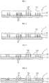
- FIG. 1 shows the original structure of a TSV wafer 1, which comprises an integrated circuit layer 11, a silicon wafer layer 12 arranged on integrated circuit layer 11, and conductive materials 13.
- Conductive materials 13 are buried in silicon wafer layer 12, are approximately perpendicular to surface 121 of silicon wafer layer 12, and connect to integrated circuit layer 11.
- end surfaces 131 of conductive materials 13 in an unpolished TSV wafer are about a couple hundred micrometers from surface 121 of silicon wafer layer 12.
- Surface 121 is subsequently polished by grinding, so that silicon wafer layer 12 is rapidly thinned, and thereby the distance between end surfaces 131 of conductive materials 13 and surface 121 of silicon wafer layer 12 is reduced to about tens of micrometers or more.
- an optional second CMP polishing step can be performed to fully and further remove layer 14 of the TSV wafer 1.
- the method of this invention comprises the step of etching the silicon wafer to expose the conductive materials 13.
- the wafer (or other silicon substrate) is contacted with the etching composition (a solution) of this invention, the top surface 121 of layer 12 of the silicon wafer above the integrated surface layer 11 is removed until the conductive materials 13 are exposed or nearly exposed.
- the final status of the finely polished TSV wafer 1 is varied depending upon the requirements for the subsequent processes. For example, end surfaces 131 of the conductive materials 13 and top surface 121 of silicon wafer layer 12 surrounding thereof may be coplanar as shown in FIG. 3 , or the end surfaces 131 may be protruding out of top surface 121 as shown in FIG. 4 .
- the conductive materials 13 may be coated with a silicon dioxide layer or a silicon nitride layer or a titanium nitride layer or a tantalum nitride layer or combinations thereof (not shown) which may be subsequently removed in later processing steps.
- the surface roughness of the top surface 121 provided by the etchant composition is important whether or not the end surfaces 131 of the conductive materials 13 protrude or are to be coplanar with the top surface. A resulting top surface with high surface roughness after treatment with the etchant composition may make it difficult for a sensor or sensors to detect the end point of the etching step.
- a resulting top surface with high surface roughness after treatment with the etchant composition may interfere with establishing or maintaining the electrical communication between the conductive materials 13 of the treated wafer and the conductive materials of an adjacent wafer, part of a wafer or packaging when a downstream integrated circuit is constructed using the treated wafer or parts of the treated wafer.
- compositions of this invention may be used in other methods requiring that a silicon layer be etched, particularly when there is silicon dioxide present on or near the same layer and it is preferred that all or most of the silicon dioxide is not removed from the wafer or other substrate at the same time that the silicon is removed using the etchant composition of this invention.
- a high silicon etch rate, low silicon dioxide etch rate and low resulting surface roughness of the treated wafer are desireable to maintain a high through-put of treated wafers; however, sometimes depending upon a wafer manufacturer's needs, one or two of those characteristics provided by the etchant composition may be more important than the other(s), meaning for example, a lower etchant rate can be tolerated if the resulting wafer surface roughness is low.
- compositions of this invention that are used in the wet etching step comprises inorganic alkali basic hydroxides selected from the group consisting of potassium hydroxide, cesium hydroxide, sodium hydroxide, rubidium hydroxide, or lithium hydroxide, and combinations thereof, wherein the inorganic alkali basic hydroxides comprises potassium hydroxide and cesium hydroxide.
- the total amount of the inorganic alkali basic hydroxides present in the composition is from 0.5 to 25 weight percent (wt %), and is typically 0.5 to 20 wt %, or 1.0 to 20 wt %, or 2.0 to 16 wt %, or 0.5 to 22 wt %, or 1 to 18 wt %, or 1 to 16 wt %, or 1 to 14 wt %, or 1 to 12 wt %, or 1 to 10 wt %, or 0.5 to 10 wt %, or 1 to 9 wt %, or 1 to 8 wt %, or 1 to 7 wt %, or 1 to 6 wt %, or 1 to 5 wt %, or 1 to 4 wt %, or 4 to 10 wt %, or 5 to 10 wt %, or 5 to 9 wt %, or 5 to 8 wt %, or 6 to 10 wt %, or 7 to 10
- the composition comprises two or more than two inorganic alkali basic hydroxides.
- the composition comprises potassium hydroxide and cesium hydroxide. It may be preferred to use at least an equal weight percent or a greater weight percent of cesium hydroxide than potassium hydroxide in the composition. In some embodiments, the weight percent of cesium hydroxide will be more than 0.6 times or more than 1.1 times, or more than 2 times, or more than 2.5 times, or more than 5.0 times, or more than 10 times, and/or may be less than about 20 times the weight percent of potassium hydroxide present in the composition.
- the weight percent of cesium hydroxide may be from more than 0.6 to less than 20 times or 1.1 to less than 20 times, or more than 2.5 to less than 20 times, or more than or more than 5 to less than 20 times, or more than 10 to less than 20 times the weight percent of potassium hydroxide present in the composition.
- the amount of cesium hydroxide will be 1 to 9.5 wt % and the amount of potassium hydroxide will be 0.1 to 2 wt %. In other embodiments the amount of cesium hydroxide will be 1 to 5 wt % and the amount of potassium hydroxide will be 0.1 to 1.5 wt %.
- the amount of cesium hydroxide will be 1 to 5 wt % and the amount of potassium hydroxide will be 0.5 to 1.3 wt %. In still other embodiments the amount of cesium hydroxide will be 1 to 5 wt % and the amount of potassium hydroxide will be 0.7 to 1.2 wt %.
- the ratio of the weight percent of cesium hydroxide to the weight percent of the potassium hydroxide in the etchant composition will be from 1 to 10, or from 2 to 9, or from 3 to 8. These compositions may be desirable when a lower resulting surface roughness of the etched wafer is particularly important.
- the weight percent of potassium hydroxide will be more than 1 time, or more than 1.1 times and/or may be less than about 5 times the weight percent of cesium hydroxide present in the composition.
- the composition additionally comprises one or more additional alkaline compounds (in addition to inorganic alkali basic hydroxides).
- the additional alkaline compounds are non-alkali.
- the additional one or more alkaline compounds may be selected to provide the desired etch rate(s) and additionally to provide a desirable surface roughness to the etched silicon.
- the additional alkaline compounds include ammonium hydroxide (NH 4 OH), tetraethylammonium hydroxide and tetramethylammonium fluoride.
- the additional alkaline compound may be used in an amount that is from 0.1 to 5 wt %, or 0.2 to 3 wt %, or 0.5 to 2 wt %, based on the total weight of the composition.
- the concentration of the additional alkaline compound may be present in an amount that is greater than 0.1 wt % but less than 5 wt % based on the total weight of the composition.
- the ratio of the weight percent of the one or more additional alkaline compounds to the total weight percent of the inorganic alkali basic hydroxides present in the composition is in the range from 0.05 to 2.0, or from 0.05 to 1.0, or from 0.03 to 0.8, or from 0.05 to 0.8, or from 0.1 to 0.8.
- the composition of this invention further comprises water.
- the water used in the composition is pure or ultrapure water, such as (de-ionized water) DI water.
- the composition may comprise any amount of water.
- water may be present in an amount greater than 70 wt %, or from 70 to 99 wt %, or from 80 to 98 wt %, or from 85 to 98 wt %, or from 88 to 98 wt %, or from 90 to 98 wt %, or from 91 to 97 wt %, or from 92 to 96 wt %, or from 93 to 95 wt %, or greater than 90 wt %, or greater than 92 wt %, or greater than 93.5 wt %, or greater than 94 wt %, or greater than 95 wt % of the composition.
- compositions of this invention may comprise optional ingredients, such as surfactants, and/or oxidizing agents, and/or solvents, and/or corrosion inhibitors.
- compositions of this invention may comprise one or more optional surfactants that may be, for examples, anionic, cationic, nonionic and zwitterionic.
- surfactants include dodecyl sulfate sodium salts, sodium lauryl sulfates, dodecyl sulfate ammonium salts, secondary alkane sulfonates (SAS), acetylenic surfactants, alkyl phenol ethoxylates, fatty alcohol ethoxylates, fatty amine ethoxylates, propylene oxide-ethylene oxide block copolymers, or ethylene diamine surfactants, and any combination thereof.
- SAS secondary alkane sulfonates
- Suitable commercially available surfactants include TRITONTM, TergitolTM, DOWFAXTM family of surfactants manufactured by Dow Chemicals and various surfactants in SURFYNOLTM, DYNOLTM, ZetasperseTM, NonidetTM, and TomadolTM surfactant families, manufactured by Air Products and Chemicals.
- Suitable surfactants may also include polymers comprising ethylene oxide (EO) and propylene oxide (PO) groups.
- EO-PO polymer is TetronicTM 90R4 from BASF Chemicals. Additional examples of some useful surfactants are disclosed in US Patent 7,591,270 . If present, the one or more surfactants may be used in any amount, typically in an amount less than 2 wt %, or from 0.001 to 2 wt% of the total composition.
- oxidizing agents that may be used in the composition of this invention, such as hydrogen peroxide; salts of chlorite, chlorate, or perchlorate; hypochlorite and other hypohalite compounds; chromate and dichromate compounds; permanganate compounds such as potassium permanganate; sodium perborate; and organosulfonic acids. If present, oxidizing agents may be used in any amount, typically in an amount less than 5 wt %, or from 0.001 to 2 wt% of the total composition.
- composition may further comprise one or more optional organic solvents, typically water soluble or water miscible organic solvents.
- water soluble or water miscible organic solvents include solvents that are able to mix with water and each other and form a homogeneous solution at standard operating temperatures and pressures.
- water soluble or water miscible organic solvents examples include, but are not limited to, ethylene glycol, propylene glycol, dipropylene glycol, 1,4-butanediol, tripropylene glycol methyl ether, tripropylene glycol monobutyl ether, propylene glycol propyl ether, diethylene glycol n-butyl ether, hexyloxypropylamine, poly(oxyethylene)diamine, dimethylsulfoxide, tetrahydrofurfuryl alcohol, glycerol, alcohols (e.g. benzyl alcohol), sulfoxides, or mixtures thereof.
- Preferred optional solvents are alcohols, diols, or mixtures thereof.
- Preferred optional solvents include glycol ethers or hydric alcohols having 2 to 8 carbon atoms, and mixtures thereof.
- One suitable monohydric alcohol having one hydroxy group, 2 to 8 carbon atoms, and optionally, a heterocyclic compound that may be used as the optional organic solvent in the compositions of this invention includes tetrahydrofufuryl alcohol (THFA).
- THFA is particularly preferred because it is biodegradable and water-miscible with high solvency. Additionally, THFA is not listed as a carcinogen and is not classified as a hazardous waste. If present, solvents may be used in any amount, typically in an amount less than 5 wt % of the total composition.
- compositions of this invention may optionally further comprise one or more corrosion inhibitors.
- corrosion inhibitors include those well known in the art for similar applications, such as those disclosed in U.S. Pat. No. 5,417,877 .
- Corrosion inhibitors may be, for example, an organic acid, an organic acid salt, a phenol, a triazole, a hydroxylamine or acid salt thereof, or a polyethyleneimine.
- corrosion inhibitors examples include anthranilic acid, gallic acid, benzoic acid, isophthalic acid, maleic acid, fumaric acid, D,L-malic acid, malonic acid, phthalic acid, ascorbic acid, maleic anhydride, phthalic anhydride, benzotriazole (BZT), resorcinol, carboxybenzotriazole, diethyl hydroxylamine and the lactic acid and citric acid salts thereof, and the like.
- corrosion inhibitors examples include catechol, t-butyl catechol, pyrogallol, and esters of gallic acid.
- Particular hydroxylamines that can be used include diethylhydroxylamine and the lactic acid and citric acid salts thereof.
- corrosion inhibitors include fructose, ammonium thiosulfate, glycine, lactic acid, tetramethylguanidine, iminodiacetic acid, and dimethylacetoacetamide.
- the corrosion inhibitor may include a weak acid having a pH ranging from about 4 to about 7. Examples of weak acids include trihydroxybenzene, dihydroxybenzene, and/or salicylhydroxamic acid.
- Corrosion inhibitors used in the composition may be selected from the group consisting of catechol, t-butyl catechol, pyrogallol, gallic acid and phenol.
- Corrosion inhibitors used in the composition may be selected from the group consisting of catechol, t-butyl catechol, and pyrogallol. Corrosion inhibitors used in the composition may be catechol or t-butyl catechol. If present, the corrosion inhibitors may be used in any amount, typically in an amount less than 5 wt % of the total composition.
- compositions of this invention are substantially free of certain components. “Substantially free of” means that the composition comprises less than 0.05 wt % of a named component or class of components. “Free of” means that the composition comprises less than 0.001 % of a named component or class of components.
- compositions of this invention may be substantially free of, or free of, one or more or all of the following in any combination: oxidizing agents, and/or organic solvents, and/or corrosion-inhibitors, and/or fluorine-containing components, and/or quaternary ammonium hydroxides, and/or alkanolamines, and/or hydroxyalmines, and/or surfactants, and/or chelating agents and/or biocides and/or thionites and/or sulfites and/or sulfates and/or polymers.
- Some embodiments of this invention may be substantially free of, or free of, oxidizing agents, and corrosion-inhibitors, and alkanolamines, and hydroxylamines, and surfactants, and chelating agents and/or thionites, sulfites, sulfates and polymers. Some embodiments of this invention may be substantially free of, or free of, oxidizing agents, corrosion-inhibitors, alkanolamines, hydroxylamines, surfactants, chelating agents, and fluorine-containing components and/or thionites, sulfites, sulfates and polymers.
- Some embodiments of this invention may be substantially free of, or free of, oxidizing agents, corrosion-inhibitors, alkanolamines, hydroxylamines, surfactants, chelating agents, fluorine-containing components, and quaternary ammonium hydroxides. Some embodiments of this invention may be substantially free of, or free of, oxidizing agents, alkanolamines, hydroxylamines, surfactants, chelating agents and fluorine-containing components. Some embodiments of this invention may be substantially free of, or free of, oxidizing agents, alkanolamines, hydroxylamines, surfactants, chelating agents, fluorine-containing components, and quaternary ammonium hydroxides.
- Some embodiments of this invention may be substantially free of, or free of, oxidizing agents, corrosion-inhibitors, alkanolamines, hydroxylamines, surfactants, chelating agents and fluorine-containing components. Any of the preceding lists may also include organic solvents therein as a component that the composition of this invention is free of or substantially free of.
- the etchant is applied only to the surface of the wafer that needs to be etched.
- a lithographic process employing a photoresist may be used to define and expose only the areas on the wafer surface where etching is desired and the etchant solution of this invention shall contact the silicon wafer surface only in those areas.
- the etchant is typically used at a temperature between between 25 and 100°C, or 25 and 90°C, in many embodiments approximately 70 °C.
- compositions of this invention provide an Si etch amount that is greater than 0.7 ⁇ m/min, or greater than 0.8 ⁇ m/min. Further, it may be desired that the compositions of this invention provide an SiO2 etch rate that is less than 0.0006 ⁇ m/min, or less than 0.0005 ⁇ m/min or less than 0.0004 ⁇ m/min. It may also be desired that the compositions of this invention provide an Si etch to SiO2 etch ratio of greater than 500 or greater than 800 or greater than 1250 or greater than 1500 or greater than 1700 or greater than 1850 or greater than 2000.
- Each etchant composition tested was heated to 70°C.
- Blank (unpatterned) p-type Si wafer segments 3.5" x 5" (8.89 cm x 12.7 cm) size were cleaved from a whole wafer with exposed [1,0,0] crystal face.
- the Si segments were pre-treated with buffered oxide etch (BOE) at an ambient temperature of approximately 22°C for 3 minutes to remove native surface oxide, rinsed in deionized water (DIW) for 3 minutes and dried with a nitrogen (N 2 ) gun. Si segments were then weighed on a balance with 5 decimal places for an accurate recording of the weight.
- BOE buffered oxide etch
- DIW deionized water
- N 2 nitrogen
- the Si segments were then immersed into the etchant for a specific amount of time, removed and rinsed in deionized water (DIW) for 3 minutes, dried with N 2 , then weighed.
- DIW deionized water
- the initial and final thicknesses were determined by assuming a Si density of 2.33 gm/cm 3 and from the area of the 3.5 cm x 5.0 cm segment.
- Etch rates in ⁇ m/min were calculated from the thickness change during the etch experiment. This method was repeated to determine the Si etch rates for the compositions reported in the tables below. (Note: The etch rates as reported are as described for the wafer segments with two exposed sides, each approximately 8.89 cm x 12.7 cm (3.5'x5'), and the edges.
- the SiO 2 etch rate was determined by averaging the measured change in thickness versus time (the 4 data points measured). This method was used to measure the SiO 2 etch rates for the compositions reported in the tables below.
- An etchant solution was prepared by adding 41.7 gms of 48 wt% KOH solution from Aldrich Chemical, i.e. 20.0 gms of KOH, to deionized water in an HDPE bottle and making up to 1000 gms.
- the KOH was the inorganic alkali basic hydroxide in the etchant.
- the solution was stirred to completely mix the KOH solution and had a pH of 13.05.
- About 300 gms of the solution was placed into a 500 ml beaker and strirred at 900 rpm with 1" (2.5 cm) stir bar, then heated to, and equilibriated, at 70°C while stirring.
- p-type Si wafers from LG Siltron with resistivity in the range of 1 to 35 Ohm-cm were used in this test.
- Two p-type Si wafer segments were cleaved from Siltron wafers, pretreated and weighed. One segment was immersed for 10 minutes and the second segment for 60 minutes, each was removed and rinsed with DIW for 3 mins, and dried. The segments were then re-weighed after drying. This etchant gave a Si etch rate of 0.99 ⁇ m/min (calculated from the two weight measurements), an SiO 2 etch rate of 0.00091 ⁇ m/min, and Si/SiO 2 selectivity ratio of 1088.
- Etchant solutions were prepared as in Comparative Example 1 except that the weight percents of KOH, as the inorganic alkali basic hydroxide, and tetraethylammonium hydroxide (TEAH), as the additional alkaline compound, and deionized water used to make each 1000 gm composition were as indicated in Table 1 below.
- the TEAH was obtained as a 50 wt% solution in water from Sachem.
- the solutions were stirred to completely mix the solutions.
- the same tests described for Comparative Example 1 were repeated using the Example 1-4 compositions.
- the Si etch rate, the SiO 2 etch rate and the Si/SiO 2 etch rate ratio measured and calculated as described above using each of the Example 1-4 compositions are listed in Table 1.
- Examples 5-7 An etchant solution was prepared as described for Examples 1-4 above, except that the component weight percentages that are in Table 1 were used and the compositions further included adding cesium hydroxide (CsOH) to the KOH, tetraethylammonium hydroxide (TEAH) and deionized water in a HDPE bottle to make 1000 gms of each of the compositions.
- CsOH cesium hydroxide
- TEAH tetraethylammonium hydroxide
- deionized water in a HDPE bottle to make 1000 gms of each of the compositions.
- the CsOH was obtained as a 50 wt% solution in water from Aldrich.
- the Si etch rate, the SiO 2 etch rate and the Si/SiO 2 etch rate ratio for each of the compositions of Examples 5-7 were determined as described above and are listed in Table 1.
- Example 8 An etchant solution was prepared as described for Example 1 above, except that 1.0 gm of Pluronic® L31 a difunctional block copolymer surfactant terminating in primary hydroxyl groups was added to the composition and the amount of water therein was adjusted accordingly. (Pluronic is a registered trademark of BASF Corporation.) The Si etch rate, the SiO 2 etch rate and the Si/SiO 2 etch rate ratio for Example 8 were determined as described above and are listed in Table 1. Table 1 (Examples 1 to 4 and 8 are comparative examples) Comp -osition No.
- inorganic alkali basic hydroxide KOH (wt %) inorganic alkali basic hydroxide CsOH (wt %) additional alkaline compound TEAH (wt %) DI water (wt %) surfactant (wt %) Si etch rate ( ⁇ m/min) SiO 2 etch rate ( ⁇ m/min) Si/SiO 2 etch rate Comparative Ex.
- Etchant solutions were prepared as described in Example 1 except that the additional alkaline compounds listed in Table 2 were used in the amounts indicated in Table 2 in the etchant compositions.
- Table 2 also indicates the amount of KOH and water used for each of the etchant compositions.
- TMAF tetramethylammonium fluoride
- NH 4 OH ammonium hydroxide
- LiOH lithium hydroxide
- KCI potassium chloride
- La Acetate lanthanum acetate
- BaCl 2 barium chloride
- inorganic alkali basic hydroxide KOH (wt %) inorganic alkali basic hydroxide CsOH (wt %) additional alkaline compound amount of additional alkaline compound (wt %) DI water (wt %) Si etch rate (um/min) 15 2 0 TMAF 0.83 97.17 0.98 16 2 0 TMAF 1.66 96.34 1.19 17 2 0 TMAF 3.32 94.68 0.98 18 2 0 NH 4 OH 0.31 97.69 1.10 19 2 0 NH 4 OH 0.62 97.38 0.96 20 2 0 NH 4 OH 1.24 96.76 1.08 21 2 LiOH* 4.3 93.7 0.758 22 2 0 KCl 1.33 96.67 0.506 23 2 0 La Acetate 1.88 96.12 0.650 24 2 0 BaCl 2 1.86 96.14 ⁇ 0 * LiOH was used in this composition instead of CsOH.
- Etching compositions were prepared as described in the examples above, the components and their corresponding weight percents are listed in Table 3.
- Etched wafer samples were prepared by immersing wafer segments for 10 minutes in the etching compositions as described in Comparative Example 1. The surface roughness of the wafer segments were analyzed as follows. Atomic force microscopy (AFM) was performed using a Digital Instruments Dimension 3000 interfaced to a Nanoscope IIIa controller. All measurements were obtained in tapping mode (0.3 - 0.5 Hz scan rate) with single cantilever etched silicon SPM probes (Bruker, NCHV). The scan area used was 40 ⁇ m x 40 ⁇ m.
- Root-mean-square (RMS) values calculated using the generalized formula shown in the "Scanning Probe Microscopy Training Notebook, Digital Instruments", Veeco Metrology Group, 2000, Version 3.0, 004-130-000 (standard issue) / 004-130-100 (cleanroom issue) for each imaged area.
- Table 3 Composition No. inorganic alkali basic hydroxide KOH (wt %) inorganic alkali basic hydroxide CsOH (wt %) additional alkaline compound TEAH (wt %) DI water (wt %) Location Surface Roughness (nm) 25 10 0 2.62 63.8 1 36.4 1 2 0 2.62 95.38 1 33.6 1 2 0 2.62 95.38 2 32.5 6 1 2.67 2.62 93.71 1 115 6 1 2.67 2.62 93.71 2 116 5 2 1.33 2.62 94.05 1 36.6 5 2 1.33 2.62 94.05 2 45.9
- Example 1 and 25 are comparative examples
- Examples 35A to 35M are shown below in Table 4.
- Example 35A through 35E and 35K to 35M are comparative examples
- Example 20D through 20F are comparative examples
- the test method described above for Comparative Example 1 was used except that the compositions described in the table below were used.
- the Si etch rate, the SiO 2 etch rate and the Si/SiO 2 etch rate ratio for each of the compositions were determined as described above and are listed below in the table.
- the surface roughness was determined based on SEMs that were taken. After immersion the Si wafer substrates were rinsed with DI water for 3 minutes at ambient and dried with Nitrogen. The treated substrates were photographed using an SEM at 2kV acceleration voltage and 2k and 10 magnification. The SEM photographs were then visually inspected and rated using the following ratings:
- ⁇ smooth surface and/or few small Si crystallites here and there on surface.
- ⁇ small Si crystallites covering most of surface and/or few medium crystallites.
- ⁇ either few large or many medium size Si crystallites.
- SAS-10 is a 10% solution of secondary alkane sulfonates.
Landscapes
- Chemical & Material Sciences (AREA)
- Engineering & Computer Science (AREA)
- Materials Engineering (AREA)
- Organic Chemistry (AREA)
- Chemical Kinetics & Catalysis (AREA)
- General Chemical & Material Sciences (AREA)
- Mechanical Engineering (AREA)
- Metallurgy (AREA)
- Cleaning Or Drying Semiconductors (AREA)
- Weting (AREA)
- Mechanical Treatment Of Semiconductor (AREA)
Claims (10)
- Ätzzusammensetzung, umfassend:anorganische basische Alkalihydroxide, ausgewählt aus der aus Kaliumhydroxid, Cäsiumhydroxid, Natriumhydroxid, Rubidiumhydroxid oder Lithiumhydroxid bestehenden Gruppe;eine oder mehr als eine zusätzliche alkalische Verbindung, ausgewählt aus der aus Tetraethylammoniumhydroxid, Tetramethylammoniumfluorid und NH4OH bestehenden Gruppe;gegebenenfalls einen oder mehr Korrosionsinhibitoren; undWasser;wobei die anorganischen basischen Alkalihydroxide Kaliumhydroxid und Cäsiumhydroxid umfassen,wobei die Gesamtmenge der anorganischen basischen Alkalihydroxide 0,5 bis 25 Gew.-% beträgt; undwobei die Zusammensetzung vorrangig Silicium, welches auf einem Substrat vorhanden ist, verglichen mit Siliciumdioxid, welches auf dem Substrat vorhanden ist, ätzt.
- Ätzzusammensetzung nach Anspruch 1, wobei das eine oder die mehr anorganischen basischen Alkalihydroxide in einer Gesamtmenge von 1 bis 20 Gew.-% der Gesamtzusammensetzung vorhanden sind.
- Ätzzusammensetzung nach den Ansprüchen 1 oder 2, wobei der eine oder die mehr Korrosionsinhibitoren in der Zusammensetzung vorhanden sind und der eine oder die mehr Korrosionsinhibitoren aus der aus Anthranilsäure, Gallussäure, Benzoesäure, Isophthalsäure, Maleinsäure, Fumarsäure, D,L-Äpfelsäure, Malonsäure, Phthalsäure, Ascorbinsäure, Maleinsäureanhydrid, Phthalsäureanhydrid, Benzotriazol, Resorcinol, Carboxybenzotriazol, Milchsäure, Zitronensäure, Catechin, t-Butylcatechol, Pyrogallol, Estern von Gallussäure, Phenol, Glycin, Tetramethylguanidin, Iminodiessigsäure und Dimethylacetoacetamid, Trihydroxybenzen, Dihydroxybenzen und Salicylhydroxamsäure bestehenden Gruppe ausgewählt sind, bevorzugt aus der aus Catechin, t-Butylcatechol, Pyrogallol, Gallussäure und Phenol bestehenden Gruppe ausgewählt sind, und stärker bevorzugt aus der aus Catechin und t-Butylcatechol bestehenden Gruppe ausgewählt sind.
- Ätzzusammensetzung nach den Ansprüchen 1 bis 3, wobei die eine oder mehr zusätzlichen alkalischen Verbindungen in der Zusammensetzung von 0,1 bis 5 Gew.-%, bevorzugt von 0,2 bis 3 Gew.-% vorhanden sind.
- Ätzzusammensetzung nach den Ansprüchen 1 bis 4, wobei die Zusammensetzung 70 bis 99 Gew.-% Wasser, bezogen auf das Gesamtgewicht der Zusammensetzung, bevorzugt 80 bis 98 Gew.-% Wasser, bezogen auf das Gesamtgewicht der Zusammensetzung, umfasst.
- Ätzzusammensetzung nach den Ansprüchen 1 bis 5, wobei die Zusammensetzung weniger als 0,05 Gew.-% von den Folgenden umfasst oder frei von einem oder mehr oder allen davon ist: grenzflächenaktiven Mitteln, chelatbildenden Mitteln, oxidierenden Mitteln, Lösungsmitteln und Bioziden.
- Verfahren zur Herstellung eines Siliciumsubstrats, wobei das Verfahren umfasst: Bilden eines Siliciumdioxidfilms auf einem Siliciumsubstrat, wobei der Siliciumdioxidfilm mindestens eine Öffnung in dem Siliciumdioxidfilm auf mindestens einer Oberfläche des Siliciumsubstrats aufweist; einen ersten Ätzschritt zum Ätzen des Siliciumsubstrats an der mindestens einen Öffnung unter Verwendung der Zusammensetzung nach Anspruch 1, wobei der Siliciumdioxidfilm als eine Maske wirkt, wobei der erste Ätzschritt zum Bilden einer Silicium-Durchkontaktierung verwendet wird.
- Verfahren nach Anspruch 7, ferner umfassend den Schritt von Schichtbilden eines Titannitridfilms auf dem Siliciumdioxidfilm, wobei der Titannitridfilm auch mit mindestens einer Öffnung gebildet wird, wobei mindestens eine der mindestens einen Titannitridöffnung und mindestens eine der mindestens einen Siliciumdioxidöffnung ausgerichtet sind.
- Verfahren nach den Ansprüchen 7 oder 8, ferner umfassend vor dem ersten Ätzschritt einen zweiten Ätzschritt zum Bilden von einem oder mehr Löchern in dem Siliciumsubstrat, wobei das eine oder die mehr Löcher nicht über die Oberfläche des Siliciumsubstrats hinausragen; und wobei während dem ersten Ätzschritt das eine oder die mehr Löcher mit der mindestens einen Öffnung in dem auf dem Siliciumsubstrat gebildeten Siliciumdioxidfilm ausgerichtet sind.
- Verfahren gemäß den Ansprüchen 7 bis 9, ferner umfassend den Schritt von Füllen des einen oder der mehr Löcher mit Kupfer vor oder nach dem ersten Ätzschritt oder nach dem zweiten Ätzschritt.
Applications Claiming Priority (2)
| Application Number | Priority Date | Filing Date | Title |
|---|---|---|---|
| US201462097408P | 2014-12-29 | 2014-12-29 | |
| US14/978,383 US9873833B2 (en) | 2014-12-29 | 2015-12-22 | Etchant solutions and method of use thereof |
Publications (2)
| Publication Number | Publication Date |
|---|---|
| EP3040397A1 EP3040397A1 (de) | 2016-07-06 |
| EP3040397B1 true EP3040397B1 (de) | 2021-06-30 |
Family
ID=55361303
Family Applications (1)
| Application Number | Title | Priority Date | Filing Date |
|---|---|---|---|
| EP15202875.9A Active EP3040397B1 (de) | 2014-12-29 | 2015-12-29 | Ätzlösungen und verfahren zur verwendung davon |
Country Status (9)
| Country | Link |
|---|---|
| US (1) | US9873833B2 (de) |
| EP (1) | EP3040397B1 (de) |
| JP (2) | JP6809787B2 (de) |
| KR (3) | KR20160080084A (de) |
| CN (1) | CN105733587B (de) |
| MY (1) | MY180929A (de) |
| PH (1) | PH12016000004B1 (de) |
| SG (1) | SG10201510712PA (de) |
| TW (1) | TWI580764B (de) |
Families Citing this family (33)
| Publication number | Priority date | Publication date | Assignee | Title |
|---|---|---|---|---|
| TWI642763B (zh) * | 2014-01-27 | 2018-12-01 | Mitsubishi Gas Chemical Company, Inc. | 氮化鈦除去用液體組成物、利用該液體組成物之半導體元件之洗滌方法、及半導體元件之製造方法 |
| US9976111B2 (en) * | 2015-05-01 | 2018-05-22 | Versum Materials Us, Llc | TiN hard mask and etch residual removal |
| US10072237B2 (en) | 2015-08-05 | 2018-09-11 | Versum Materials Us, Llc | Photoresist cleaning composition used in photolithography and a method for treating substrate therewith |
| KR102532413B1 (ko) * | 2016-07-21 | 2023-05-15 | 동우 화인켐 주식회사 | 폴리실리콘 식각액 조성물 및 반도체 소자의 제조방법 |
| KR102668708B1 (ko) * | 2016-09-05 | 2024-05-23 | 동우 화인켐 주식회사 | 폴리실리콘 식각액 조성물 및 반도체 소자의 제조 방법 |
| KR102368969B1 (ko) * | 2017-03-30 | 2022-03-02 | 동우 화인켐 주식회사 | 식각액 조성물 및 이를 이용한 디스플레이 장치용 어레이 기판의 제조방법 |
| US10934485B2 (en) * | 2017-08-25 | 2021-03-02 | Versum Materials Us, Llc | Etching solution for selectively removing silicon over silicon-germanium alloy from a silicon-germanium/ silicon stack during manufacture of a semiconductor device |
| US10761423B2 (en) | 2017-08-30 | 2020-09-01 | Taiwan Semiconductor Manufacturing Company, Ltd. | Chemical composition for tri-layer removal |
| CN108085683A (zh) * | 2018-01-22 | 2018-05-29 | 深圳市华星光电技术有限公司 | 一种蚀刻液组合物 |
| US11180697B2 (en) * | 2018-11-19 | 2021-11-23 | Versum Materials Us, Llc | Etching solution having silicon oxide corrosion inhibitor and method of using the same |
| TWI683362B (zh) * | 2018-12-17 | 2020-01-21 | 許富翔 | 矽鰭片結構的修整方法 |
| KR20210107656A (ko) * | 2018-12-18 | 2021-09-01 | 가부시키가이샤 도쿠야마 | 실리콘 에칭액 |
| CN110438504A (zh) * | 2019-08-19 | 2019-11-12 | 江阴江化微电子材料股份有限公司 | 一种铝栅刻开区硅渣清除组合物及硅渣清除方法 |
| CN112480928A (zh) * | 2019-09-11 | 2021-03-12 | 利绅科技股份有限公司 | 硅蚀刻组成物及其作用于硅基材的蚀刻方法 |
| JP7668790B2 (ja) | 2019-09-30 | 2025-04-25 | バーサム マテリアルズ ユーエス,リミティド ライアビリティ カンパニー | フォトレジスト除去剤 |
| CN110922970A (zh) * | 2019-11-29 | 2020-03-27 | 南京纳鑫新材料有限公司 | 一种perc电池背抛光添加剂及工艺 |
| CN111440613B (zh) * | 2019-12-09 | 2022-03-25 | 杭州格林达电子材料股份有限公司 | 一种tmah系各向异性硅蚀刻液及其制备方法 |
| CN111341655A (zh) * | 2020-03-07 | 2020-06-26 | 浙江中晶科技股份有限公司 | 一种重掺硼硅片双次碱腐蚀加工工艺 |
| CN113736466B (zh) * | 2020-05-29 | 2023-05-12 | 新应材股份有限公司 | 蚀刻剂组合物、增粘剂、移除聚酰亚胺的方法以及蚀刻工艺 |
| TWI751568B (zh) | 2020-05-29 | 2022-01-01 | 新應材股份有限公司 | 蝕刻劑組成物、增黏劑、鹼溶液、移除聚醯亞胺的方法以及蝕刻製程 |
| JPWO2022138754A1 (de) | 2020-12-24 | 2022-06-30 | ||
| CN113161234B (zh) * | 2021-04-27 | 2023-02-17 | 上海新阳半导体材料股份有限公司 | 一种含氟清洗液组合物的应用 |
| CN113186044B (zh) * | 2021-04-27 | 2022-12-30 | 上海新阳半导体材料股份有限公司 | 一种含氟清洗液组合物的制备方法 |
| US11920252B2 (en) | 2021-08-05 | 2024-03-05 | Toyota Motor Engineering & Manufacturing North America, Inc. | SU-8 etching technique using molten salt |
| JP7757096B2 (ja) * | 2021-09-14 | 2025-10-21 | 株式会社東芝 | エッチング方法 |
| CN114854419B (zh) * | 2022-04-13 | 2023-09-05 | 华中科技大学 | 一种用于湿法蚀刻相变材料的碱性蚀刻液及其应用 |
| CN114989825B (zh) * | 2022-06-30 | 2023-07-11 | 湖北兴福电子材料股份有限公司 | 一种掺钪氮化铝和钨的选择性蚀刻液 |
| CN115011347B (zh) * | 2022-06-30 | 2023-12-29 | 湖北兴福电子材料股份有限公司 | 一种氮化铝和钨的选择性蚀刻液 |
| CN115044376B (zh) * | 2022-06-30 | 2023-12-29 | 湖北兴福电子材料股份有限公司 | 一种掺钪氮化铝蚀刻液及其应用 |
| CN115595154B (zh) * | 2022-08-31 | 2024-08-13 | 湖北兴福电子材料股份有限公司 | 一种SiGe和Si的选择性蚀刻液 |
| CN115851134B (zh) * | 2022-10-27 | 2024-09-10 | 万华化学集团电子材料有限公司 | 一种高精度硅片抛光组合物及其应用 |
| WO2025199009A1 (en) * | 2024-03-21 | 2025-09-25 | Fujifilm Electronic Materials U.S.A., Inc. | Etching compositions |
| CN120718655B (zh) * | 2025-08-19 | 2025-10-28 | 张家港安储科技有限公司 | 一种碱性硅蚀刻液及其应用 |
Family Cites Families (27)
| Publication number | Priority date | Publication date | Assignee | Title |
|---|---|---|---|---|
| BE789090A (fr) * | 1971-09-22 | 1973-01-15 | Western Electric Co | Procede et solution d'attaque de semi-conducteurs |
| US3980587A (en) * | 1974-08-16 | 1976-09-14 | G. T. Schjeldahl Company | Stripper composition |
| JPH03201533A (ja) | 1989-12-28 | 1991-09-03 | Toyota Central Res & Dev Lab Inc | シリコンの異方性エッチング液 |
| JP3160344B2 (ja) | 1991-01-25 | 2001-04-25 | アシュランド インコーポレーテッド | 有機ストリッピング組成物 |
| JP3525612B2 (ja) | 1996-03-12 | 2004-05-10 | セイコーエプソン株式会社 | シリコンウェハーの加工方法及びそのシリコンウェハーを用いた電子機器 |
| US7129199B2 (en) | 2002-08-12 | 2006-10-31 | Air Products And Chemicals, Inc. | Process solutions containing surfactants |
| JP4631152B2 (ja) | 2000-03-16 | 2011-02-16 | 株式会社デンソー | シリコン基板を用いた半導体装置の製造方法 |
| JP3890981B2 (ja) | 2002-01-07 | 2007-03-07 | 株式会社Sumco | アルカリエッチング液及びこのエッチング液を用いたシリコンウェーハのエッチング方法並びにこの方法を用いたシリコンウェーハの表裏面差別化方法 |
| JP5109261B2 (ja) | 2006-02-10 | 2012-12-26 | 三菱瓦斯化学株式会社 | シリコン微細加工に用いるシリコン異方性エッチング剤組成物 |
| JP2007305832A (ja) * | 2006-05-12 | 2007-11-22 | Matsushita Electric Ind Co Ltd | 半導体装置の製造方法 |
| JP5142592B2 (ja) | 2007-06-06 | 2013-02-13 | 関東化学株式会社 | 基板の洗浄またはエッチングに用いられるアルカリ性水溶液組成物 |
| JP5022198B2 (ja) * | 2007-11-27 | 2012-09-12 | パナソニック株式会社 | トランスデューサ用基板の製造方法 |
| US7999335B2 (en) * | 2007-12-05 | 2011-08-16 | Semiconductor Energy Laboratory Co., Ltd. | Micromachine and method for manufacturing the same |
| JP5302551B2 (ja) * | 2008-02-28 | 2013-10-02 | 林純薬工業株式会社 | シリコン異方性エッチング液組成物 |
| JP5379441B2 (ja) | 2008-10-09 | 2013-12-25 | 関東化学株式会社 | 基板処理用アルカリ性水溶液組成物 |
| JP5339880B2 (ja) * | 2008-12-11 | 2013-11-13 | 株式会社新菱 | シリコン基板のエッチング液およびシリコン基板の表面加工方法 |
| US8883034B2 (en) | 2009-09-16 | 2014-11-11 | Brian Reiss | Composition and method for polishing bulk silicon |
| WO2011040484A1 (ja) | 2009-10-02 | 2011-04-07 | 三菱瓦斯化学株式会社 | シリコンエッチング液およびエッチング方法 |
| EP2355138B1 (de) * | 2010-01-28 | 2016-08-24 | Canon Kabushiki Kaisha | FLÜSSIGKEITSZUSAMMENSETZUNG, VERFAHREN ZUR HERSTELLUNG EINES SILIZIUMSUBSTRATS UND VERFAHREN ZUR HERSTELLUNG EINES FLÜSSIGKEITSAUSSTOßKOPFSUBSTRATS |
| JP6040029B2 (ja) * | 2010-09-24 | 2016-12-07 | 株式会社フジミインコーポレーテッド | 研磨用組成物及び研磨方法 |
| JP5869368B2 (ja) * | 2011-03-04 | 2016-02-24 | 富士フイルム株式会社 | キャパシタ構造の形成方法及びこれに用いられるシリコンエッチング液 |
| JP2012209480A (ja) * | 2011-03-30 | 2012-10-25 | Disco Abrasive Syst Ltd | 電極が埋設されたウエーハの加工方法 |
| JP2013168610A (ja) * | 2012-02-17 | 2013-08-29 | Tokuyama Corp | テクスチャー形成用組成物、シリコン基板の製造方法、及びテクスチャー形成用組成物調製キット |
| US20130295712A1 (en) * | 2012-05-03 | 2013-11-07 | Advanced Technology Materials, Inc. | Methods of texturing surfaces for controlled reflection |
| JP5943755B2 (ja) * | 2012-07-20 | 2016-07-05 | キヤノン株式会社 | 液体吐出ヘッドの基板の製造方法 |
| JP2014033046A (ja) * | 2012-08-02 | 2014-02-20 | Tokuyama Corp | テクスチャー形成用組成物、シリコン基板の製造方法、及びテクスチャー形成用組成物調製キット |
| JP6146144B2 (ja) | 2013-06-03 | 2017-06-14 | 富士通株式会社 | 半導体装置およびその製造方法。 |
-
2015
- 2015-12-22 US US14/978,383 patent/US9873833B2/en active Active
- 2015-12-24 TW TW104143649A patent/TWI580764B/zh active
- 2015-12-28 JP JP2015257092A patent/JP6809787B2/ja active Active
- 2015-12-28 MY MYPI2015704773A patent/MY180929A/en unknown
- 2015-12-28 KR KR1020150187290A patent/KR20160080084A/ko not_active Ceased
- 2015-12-29 CN CN201511009473.9A patent/CN105733587B/zh active Active
- 2015-12-29 SG SG10201510712PA patent/SG10201510712PA/en unknown
- 2015-12-29 EP EP15202875.9A patent/EP3040397B1/de active Active
-
2016
- 2016-01-04 PH PH12016000004A patent/PH12016000004B1/en unknown
-
2018
- 2018-06-04 KR KR1020180064229A patent/KR102285187B1/ko active Active
- 2018-12-07 JP JP2018230185A patent/JP6932683B2/ja active Active
-
2021
- 2021-07-27 KR KR1020210098701A patent/KR102378486B1/ko active Active
Non-Patent Citations (1)
| Title |
|---|
| None * |
Also Published As
| Publication number | Publication date |
|---|---|
| KR102378486B1 (ko) | 2022-03-23 |
| PH12016000004A1 (en) | 2017-07-10 |
| TW201623581A (zh) | 2016-07-01 |
| CN105733587A (zh) | 2016-07-06 |
| JP6932683B2 (ja) | 2021-09-08 |
| SG10201510712PA (en) | 2016-07-28 |
| US9873833B2 (en) | 2018-01-23 |
| CN105733587B (zh) | 2020-04-03 |
| KR20160080084A (ko) | 2016-07-07 |
| KR20210095845A (ko) | 2021-08-03 |
| PH12016000004B1 (en) | 2017-07-10 |
| JP2019068087A (ja) | 2019-04-25 |
| JP6809787B2 (ja) | 2021-01-06 |
| KR20180064365A (ko) | 2018-06-14 |
| JP2016127293A (ja) | 2016-07-11 |
| MY180929A (en) | 2020-12-12 |
| KR102285187B1 (ko) | 2021-08-02 |
| EP3040397A1 (de) | 2016-07-06 |
| TWI580764B (zh) | 2017-05-01 |
| US20160186058A1 (en) | 2016-06-30 |
Similar Documents
| Publication | Publication Date | Title |
|---|---|---|
| KR102378486B1 (ko) | 에칭제 용액 및 이를 사용하는 방법 | |
| CN111356759B (zh) | 剥离剂溶液和使用剥离剂溶液的方法 | |
| US8642526B2 (en) | Composition and method for recycling semiconductor wafers having low-k dielectric materials thereon | |
| US11149231B2 (en) | Cleaning liquid, cleaning method, and method for producing semiconductor wafer | |
| KR101997950B1 (ko) | 반도체 디바이스용 세정액 및 반도체 디바이스용 기판의 세정 방법 | |
| CN111225965B (zh) | 蚀刻组合物 | |
| TW201920765A (zh) | 於製造一半導體裝置時用於從矽-鍺/矽堆疊同時移除矽及矽-鍺合金的蝕刻組合物 | |
| EP1991637A2 (de) | Selektivabtragungschemien für halbleiteranwendungen, herstellungsverfahren und verwendung | |
| JP2016127291A (ja) | 高いwn/w選択率を有するストリッピング組成物 | |
| JP2019050364A (ja) | 半導体デバイスの製造中にシリコン−ゲルマニウム/シリコン積層体からシリコン−ゲルマニウム合金に対してシリコンを選択的に除去するためのエッチング液 | |
| CN109423290B (zh) | 用于在制造半导体器件过程中相对于氮化钛选择性地去除氮化钽的蚀刻溶液 | |
| WO2006054996A1 (en) | Selective removal chemistries for semiconductor applications, methods of production and uses thereof | |
| CN108473918A (zh) | 用于化学机械抛光后清洁的组合物 | |
| US20190144781A1 (en) | Composition for post chemical-mechanical-polishing cleaning | |
| JP2023540253A (ja) | 洗浄組成物 |
Legal Events
| Date | Code | Title | Description |
|---|---|---|---|
| PUAI | Public reference made under article 153(3) epc to a published international application that has entered the european phase |
Free format text: ORIGINAL CODE: 0009012 |
|
| AK | Designated contracting states |
Kind code of ref document: A1 Designated state(s): AL AT BE BG CH CY CZ DE DK EE ES FI FR GB GR HR HU IE IS IT LI LT LU LV MC MK MT NL NO PL PT RO RS SE SI SK SM TR |
|
| AX | Request for extension of the european patent |
Extension state: BA ME |
|
| STAA | Information on the status of an ep patent application or granted ep patent |
Free format text: STATUS: REQUEST FOR EXAMINATION WAS MADE |
|
| 17P | Request for examination filed |
Effective date: 20161026 |
|
| RBV | Designated contracting states (corrected) |
Designated state(s): AL AT BE BG CH CY CZ DE DK EE ES FI FR GB GR HR HU IE IS IT LI LT LU LV MC MK MT NL NO PL PT RO RS SE SI SK SM TR |
|
| RAP1 | Party data changed (applicant data changed or rights of an application transferred) |
Owner name: VERSUM MATERIALS US, LLC |
|
| STAA | Information on the status of an ep patent application or granted ep patent |
Free format text: STATUS: EXAMINATION IS IN PROGRESS |
|
| 17Q | First examination report despatched |
Effective date: 20171122 |
|
| REG | Reference to a national code |
Ref country code: DE Ref legal event code: R079 Ref document number: 602015070819 Country of ref document: DE Free format text: PREVIOUS MAIN CLASS: C09K0013020000 Ipc: H01L0021768000 |
|
| GRAP | Despatch of communication of intention to grant a patent |
Free format text: ORIGINAL CODE: EPIDOSNIGR1 |
|
| STAA | Information on the status of an ep patent application or granted ep patent |
Free format text: STATUS: GRANT OF PATENT IS INTENDED |
|
| INTG | Intention to grant announced |
Effective date: 20210112 |
|
| RIC1 | Information provided on ipc code assigned before grant |
Ipc: H01L 21/768 20060101AFI20201214BHEP Ipc: C09K 13/02 20060101ALI20201214BHEP Ipc: H01L 21/306 20060101ALI20201214BHEP |
|
| GRAS | Grant fee paid |
Free format text: ORIGINAL CODE: EPIDOSNIGR3 |
|
| GRAA | (expected) grant |
Free format text: ORIGINAL CODE: 0009210 |
|
| STAA | Information on the status of an ep patent application or granted ep patent |
Free format text: STATUS: THE PATENT HAS BEEN GRANTED |
|
| AK | Designated contracting states |
Kind code of ref document: B1 Designated state(s): AL AT BE BG CH CY CZ DE DK EE ES FI FR GB GR HR HU IE IS IT LI LT LU LV MC MK MT NL NO PL PT RO RS SE SI SK SM TR |
|
| REG | Reference to a national code |
Ref country code: CH Ref legal event code: EP |
|
| REG | Reference to a national code |
Ref country code: DE Ref legal event code: R096 Ref document number: 602015070819 Country of ref document: DE Ref country code: AT Ref legal event code: REF Ref document number: 1407132 Country of ref document: AT Kind code of ref document: T Effective date: 20210715 |
|
| REG | Reference to a national code |
Ref country code: IE Ref legal event code: FG4D |
|
| REG | Reference to a national code |
Ref country code: LT Ref legal event code: MG9D |
|
| PG25 | Lapsed in a contracting state [announced via postgrant information from national office to epo] |
Ref country code: BG Free format text: LAPSE BECAUSE OF FAILURE TO SUBMIT A TRANSLATION OF THE DESCRIPTION OR TO PAY THE FEE WITHIN THE PRESCRIBED TIME-LIMIT Effective date: 20210930 Ref country code: HR Free format text: LAPSE BECAUSE OF FAILURE TO SUBMIT A TRANSLATION OF THE DESCRIPTION OR TO PAY THE FEE WITHIN THE PRESCRIBED TIME-LIMIT Effective date: 20210630 Ref country code: FI Free format text: LAPSE BECAUSE OF FAILURE TO SUBMIT A TRANSLATION OF THE DESCRIPTION OR TO PAY THE FEE WITHIN THE PRESCRIBED TIME-LIMIT Effective date: 20210630 |
|
| REG | Reference to a national code |
Ref country code: NL Ref legal event code: MP Effective date: 20210630 |
|
| REG | Reference to a national code |
Ref country code: AT Ref legal event code: MK05 Ref document number: 1407132 Country of ref document: AT Kind code of ref document: T Effective date: 20210630 |
|
| PG25 | Lapsed in a contracting state [announced via postgrant information from national office to epo] |
Ref country code: SE Free format text: LAPSE BECAUSE OF FAILURE TO SUBMIT A TRANSLATION OF THE DESCRIPTION OR TO PAY THE FEE WITHIN THE PRESCRIBED TIME-LIMIT Effective date: 20210630 Ref country code: RS Free format text: LAPSE BECAUSE OF FAILURE TO SUBMIT A TRANSLATION OF THE DESCRIPTION OR TO PAY THE FEE WITHIN THE PRESCRIBED TIME-LIMIT Effective date: 20210630 Ref country code: NO Free format text: LAPSE BECAUSE OF FAILURE TO SUBMIT A TRANSLATION OF THE DESCRIPTION OR TO PAY THE FEE WITHIN THE PRESCRIBED TIME-LIMIT Effective date: 20210930 Ref country code: LV Free format text: LAPSE BECAUSE OF FAILURE TO SUBMIT A TRANSLATION OF THE DESCRIPTION OR TO PAY THE FEE WITHIN THE PRESCRIBED TIME-LIMIT Effective date: 20210630 Ref country code: GR Free format text: LAPSE BECAUSE OF FAILURE TO SUBMIT A TRANSLATION OF THE DESCRIPTION OR TO PAY THE FEE WITHIN THE PRESCRIBED TIME-LIMIT Effective date: 20211001 |
|
| PG25 | Lapsed in a contracting state [announced via postgrant information from national office to epo] |
Ref country code: AT Free format text: LAPSE BECAUSE OF FAILURE TO SUBMIT A TRANSLATION OF THE DESCRIPTION OR TO PAY THE FEE WITHIN THE PRESCRIBED TIME-LIMIT Effective date: 20210630 Ref country code: RO Free format text: LAPSE BECAUSE OF FAILURE TO SUBMIT A TRANSLATION OF THE DESCRIPTION OR TO PAY THE FEE WITHIN THE PRESCRIBED TIME-LIMIT Effective date: 20210630 Ref country code: NL Free format text: LAPSE BECAUSE OF FAILURE TO SUBMIT A TRANSLATION OF THE DESCRIPTION OR TO PAY THE FEE WITHIN THE PRESCRIBED TIME-LIMIT Effective date: 20210630 Ref country code: PT Free format text: LAPSE BECAUSE OF FAILURE TO SUBMIT A TRANSLATION OF THE DESCRIPTION OR TO PAY THE FEE WITHIN THE PRESCRIBED TIME-LIMIT Effective date: 20211102 Ref country code: ES Free format text: LAPSE BECAUSE OF FAILURE TO SUBMIT A TRANSLATION OF THE DESCRIPTION OR TO PAY THE FEE WITHIN THE PRESCRIBED TIME-LIMIT Effective date: 20210630 Ref country code: SK Free format text: LAPSE BECAUSE OF FAILURE TO SUBMIT A TRANSLATION OF THE DESCRIPTION OR TO PAY THE FEE WITHIN THE PRESCRIBED TIME-LIMIT Effective date: 20210630 Ref country code: SM Free format text: LAPSE BECAUSE OF FAILURE TO SUBMIT A TRANSLATION OF THE DESCRIPTION OR TO PAY THE FEE WITHIN THE PRESCRIBED TIME-LIMIT Effective date: 20210630 Ref country code: EE Free format text: LAPSE BECAUSE OF FAILURE TO SUBMIT A TRANSLATION OF THE DESCRIPTION OR TO PAY THE FEE WITHIN THE PRESCRIBED TIME-LIMIT Effective date: 20210630 Ref country code: CZ Free format text: LAPSE BECAUSE OF FAILURE TO SUBMIT A TRANSLATION OF THE DESCRIPTION OR TO PAY THE FEE WITHIN THE PRESCRIBED TIME-LIMIT Effective date: 20210630 |
|
| PG25 | Lapsed in a contracting state [announced via postgrant information from national office to epo] |
Ref country code: PL Free format text: LAPSE BECAUSE OF FAILURE TO SUBMIT A TRANSLATION OF THE DESCRIPTION OR TO PAY THE FEE WITHIN THE PRESCRIBED TIME-LIMIT Effective date: 20210630 |
|
| REG | Reference to a national code |
Ref country code: DE Ref legal event code: R097 Ref document number: 602015070819 Country of ref document: DE |
|
| PG25 | Lapsed in a contracting state [announced via postgrant information from national office to epo] |
Ref country code: DK Free format text: LAPSE BECAUSE OF FAILURE TO SUBMIT A TRANSLATION OF THE DESCRIPTION OR TO PAY THE FEE WITHIN THE PRESCRIBED TIME-LIMIT Effective date: 20210630 |
|
| PLBE | No opposition filed within time limit |
Free format text: ORIGINAL CODE: 0009261 |
|
| STAA | Information on the status of an ep patent application or granted ep patent |
Free format text: STATUS: NO OPPOSITION FILED WITHIN TIME LIMIT |
|
| PG25 | Lapsed in a contracting state [announced via postgrant information from national office to epo] |
Ref country code: AL Free format text: LAPSE BECAUSE OF FAILURE TO SUBMIT A TRANSLATION OF THE DESCRIPTION OR TO PAY THE FEE WITHIN THE PRESCRIBED TIME-LIMIT Effective date: 20210630 |
|
| 26N | No opposition filed |
Effective date: 20220331 |
|
| PG25 | Lapsed in a contracting state [announced via postgrant information from national office to epo] |
Ref country code: MC Free format text: LAPSE BECAUSE OF FAILURE TO SUBMIT A TRANSLATION OF THE DESCRIPTION OR TO PAY THE FEE WITHIN THE PRESCRIBED TIME-LIMIT Effective date: 20210630 Ref country code: IT Free format text: LAPSE BECAUSE OF FAILURE TO SUBMIT A TRANSLATION OF THE DESCRIPTION OR TO PAY THE FEE WITHIN THE PRESCRIBED TIME-LIMIT Effective date: 20210630 |
|
| REG | Reference to a national code |
Ref country code: CH Ref legal event code: PL |
|
| GBPC | Gb: european patent ceased through non-payment of renewal fee |
Effective date: 20211229 |
|
| REG | Reference to a national code |
Ref country code: BE Ref legal event code: MM Effective date: 20211231 |
|
| PG25 | Lapsed in a contracting state [announced via postgrant information from national office to epo] |
Ref country code: LU Free format text: LAPSE BECAUSE OF NON-PAYMENT OF DUE FEES Effective date: 20211229 Ref country code: IE Free format text: LAPSE BECAUSE OF NON-PAYMENT OF DUE FEES Effective date: 20211229 Ref country code: GB Free format text: LAPSE BECAUSE OF NON-PAYMENT OF DUE FEES Effective date: 20211229 |
|
| PG25 | Lapsed in a contracting state [announced via postgrant information from national office to epo] |
Ref country code: FR Free format text: LAPSE BECAUSE OF NON-PAYMENT OF DUE FEES Effective date: 20211231 Ref country code: BE Free format text: LAPSE BECAUSE OF NON-PAYMENT OF DUE FEES Effective date: 20211231 |
|
| PG25 | Lapsed in a contracting state [announced via postgrant information from national office to epo] |
Ref country code: LI Free format text: LAPSE BECAUSE OF NON-PAYMENT OF DUE FEES Effective date: 20211231 Ref country code: CH Free format text: LAPSE BECAUSE OF NON-PAYMENT OF DUE FEES Effective date: 20211231 |
|
| PG25 | Lapsed in a contracting state [announced via postgrant information from national office to epo] |
Ref country code: LT Free format text: LAPSE BECAUSE OF FAILURE TO SUBMIT A TRANSLATION OF THE DESCRIPTION OR TO PAY THE FEE WITHIN THE PRESCRIBED TIME-LIMIT Effective date: 20210630 |
|
| PG25 | Lapsed in a contracting state [announced via postgrant information from national office to epo] |
Ref country code: HU Free format text: LAPSE BECAUSE OF FAILURE TO SUBMIT A TRANSLATION OF THE DESCRIPTION OR TO PAY THE FEE WITHIN THE PRESCRIBED TIME-LIMIT; INVALID AB INITIO Effective date: 20151229 |
|
| PG25 | Lapsed in a contracting state [announced via postgrant information from national office to epo] |
Ref country code: CY Free format text: LAPSE BECAUSE OF FAILURE TO SUBMIT A TRANSLATION OF THE DESCRIPTION OR TO PAY THE FEE WITHIN THE PRESCRIBED TIME-LIMIT Effective date: 20210630 |
|
| P01 | Opt-out of the competence of the unified patent court (upc) registered |
Effective date: 20230602 |
|
| PG25 | Lapsed in a contracting state [announced via postgrant information from national office to epo] |
Ref country code: MK Free format text: LAPSE BECAUSE OF FAILURE TO SUBMIT A TRANSLATION OF THE DESCRIPTION OR TO PAY THE FEE WITHIN THE PRESCRIBED TIME-LIMIT Effective date: 20210630 |
|
| PG25 | Lapsed in a contracting state [announced via postgrant information from national office to epo] |
Ref country code: MT Free format text: LAPSE BECAUSE OF FAILURE TO SUBMIT A TRANSLATION OF THE DESCRIPTION OR TO PAY THE FEE WITHIN THE PRESCRIBED TIME-LIMIT Effective date: 20210630 |
|
| REG | Reference to a national code |
Ref country code: DE Ref legal event code: R079 Ref document number: 602015070819 Country of ref document: DE Free format text: PREVIOUS MAIN CLASS: H01L0021768000 Ipc: H10W0020000000 |
|
| PG25 | Lapsed in a contracting state [announced via postgrant information from national office to epo] |
Ref country code: TR Free format text: LAPSE BECAUSE OF FAILURE TO SUBMIT A TRANSLATION OF THE DESCRIPTION OR TO PAY THE FEE WITHIN THE PRESCRIBED TIME-LIMIT Effective date: 20210630 |
|
| PGFP | Annual fee paid to national office [announced via postgrant information from national office to epo] |
Ref country code: DE Payment date: 20251126 Year of fee payment: 11 |