EP3029171A1 - Cu-ga-legierungssputtertarget und verfahren zur herstellung davon - Google Patents
Cu-ga-legierungssputtertarget und verfahren zur herstellung davon Download PDFInfo
- Publication number
- EP3029171A1 EP3029171A1 EP14831218.4A EP14831218A EP3029171A1 EP 3029171 A1 EP3029171 A1 EP 3029171A1 EP 14831218 A EP14831218 A EP 14831218A EP 3029171 A1 EP3029171 A1 EP 3029171A1
- Authority
- EP
- European Patent Office
- Prior art keywords
- phase
- sputtering target
- compound
- alloy
- atomic
- Prior art date
- Legal status (The legal status is an assumption and is not a legal conclusion. Google has not performed a legal analysis and makes no representation as to the accuracy of the status listed.)
- Withdrawn
Links
Images


Classifications
-
- C—CHEMISTRY; METALLURGY
- C23—COATING METALLIC MATERIAL; COATING MATERIAL WITH METALLIC MATERIAL; CHEMICAL SURFACE TREATMENT; DIFFUSION TREATMENT OF METALLIC MATERIAL; COATING BY VACUUM EVAPORATION, BY SPUTTERING, BY ION IMPLANTATION OR BY CHEMICAL VAPOUR DEPOSITION, IN GENERAL; INHIBITING CORROSION OF METALLIC MATERIAL OR INCRUSTATION IN GENERAL
- C23C—COATING METALLIC MATERIAL; COATING MATERIAL WITH METALLIC MATERIAL; SURFACE TREATMENT OF METALLIC MATERIAL BY DIFFUSION INTO THE SURFACE, BY CHEMICAL CONVERSION OR SUBSTITUTION; COATING BY VACUUM EVAPORATION, BY SPUTTERING, BY ION IMPLANTATION OR BY CHEMICAL VAPOUR DEPOSITION, IN GENERAL
- C23C14/00—Coating by vacuum evaporation, by sputtering or by ion implantation of the coating forming material
- C23C14/22—Coating by vacuum evaporation, by sputtering or by ion implantation of the coating forming material characterised by the process of coating
- C23C14/34—Sputtering
- C23C14/3407—Cathode assembly for sputtering apparatus, e.g. Target
- C23C14/3414—Metallurgical or chemical aspects of target preparation, e.g. casting, powder metallurgy
-
- B—PERFORMING OPERATIONS; TRANSPORTING
- B22—CASTING; POWDER METALLURGY
- B22F—WORKING METALLIC POWDER; MANUFACTURE OF ARTICLES FROM METALLIC POWDER; MAKING METALLIC POWDER; APPARATUS OR DEVICES SPECIALLY ADAPTED FOR METALLIC POWDER
- B22F3/00—Manufacture of workpieces or articles from metallic powder characterised by the manner of compacting or sintering; Apparatus specially adapted therefor ; Presses and furnaces
- B22F3/12—Both compacting and sintering
- B22F3/16—Both compacting and sintering in successive or repeated steps
-
- B—PERFORMING OPERATIONS; TRANSPORTING
- B22—CASTING; POWDER METALLURGY
- B22F—WORKING METALLIC POWDER; MANUFACTURE OF ARTICLES FROM METALLIC POWDER; MAKING METALLIC POWDER; APPARATUS OR DEVICES SPECIALLY ADAPTED FOR METALLIC POWDER
- B22F5/00—Manufacture of workpieces or articles from metallic powder characterised by the special shape of the product
-
- C—CHEMISTRY; METALLURGY
- C22—METALLURGY; FERROUS OR NON-FERROUS ALLOYS; TREATMENT OF ALLOYS OR NON-FERROUS METALS
- C22C—ALLOYS
- C22C1/00—Making non-ferrous alloys
- C22C1/04—Making non-ferrous alloys by powder metallurgy
- C22C1/0425—Copper-based alloys
-
- C—CHEMISTRY; METALLURGY
- C22—METALLURGY; FERROUS OR NON-FERROUS ALLOYS; TREATMENT OF ALLOYS OR NON-FERROUS METALS
- C22C—ALLOYS
- C22C32/00—Non-ferrous alloys containing at least 5% by weight but less than 50% by weight of oxides, carbides, borides, nitrides, silicides or other metal compounds, e.g. oxynitrides, sulfides, whether added as such or formed in situ
-
- C—CHEMISTRY; METALLURGY
- C22—METALLURGY; FERROUS OR NON-FERROUS ALLOYS; TREATMENT OF ALLOYS OR NON-FERROUS METALS
- C22C—ALLOYS
- C22C9/00—Alloys based on copper
-
- C—CHEMISTRY; METALLURGY
- C23—COATING METALLIC MATERIAL; COATING MATERIAL WITH METALLIC MATERIAL; CHEMICAL SURFACE TREATMENT; DIFFUSION TREATMENT OF METALLIC MATERIAL; COATING BY VACUUM EVAPORATION, BY SPUTTERING, BY ION IMPLANTATION OR BY CHEMICAL VAPOUR DEPOSITION, IN GENERAL; INHIBITING CORROSION OF METALLIC MATERIAL OR INCRUSTATION IN GENERAL
- C23C—COATING METALLIC MATERIAL; COATING MATERIAL WITH METALLIC MATERIAL; SURFACE TREATMENT OF METALLIC MATERIAL BY DIFFUSION INTO THE SURFACE, BY CHEMICAL CONVERSION OR SUBSTITUTION; COATING BY VACUUM EVAPORATION, BY SPUTTERING, BY ION IMPLANTATION OR BY CHEMICAL VAPOUR DEPOSITION, IN GENERAL
- C23C14/00—Coating by vacuum evaporation, by sputtering or by ion implantation of the coating forming material
- C23C14/06—Coating by vacuum evaporation, by sputtering or by ion implantation of the coating forming material characterised by the coating material
- C23C14/14—Metallic material, boron or silicon
-
- H—ELECTRICITY
- H01—ELECTRIC ELEMENTS
- H01J—ELECTRIC DISCHARGE TUBES OR DISCHARGE LAMPS
- H01J37/00—Discharge tubes with provision for introducing objects or material to be exposed to the discharge, e.g. for the purpose of examination or processing thereof
- H01J37/32—Gas-filled discharge tubes
- H01J37/34—Gas-filled discharge tubes operating with cathodic sputtering
- H01J37/3411—Constructional aspects of the reactor
- H01J37/3414—Targets
- H01J37/3426—Material
- H01J37/3429—Plural materials
-
- B—PERFORMING OPERATIONS; TRANSPORTING
- B22—CASTING; POWDER METALLURGY
- B22F—WORKING METALLIC POWDER; MANUFACTURE OF ARTICLES FROM METALLIC POWDER; MAKING METALLIC POWDER; APPARATUS OR DEVICES SPECIALLY ADAPTED FOR METALLIC POWDER
- B22F2201/00—Treatment under specific atmosphere
- B22F2201/01—Reducing atmosphere
-
- B—PERFORMING OPERATIONS; TRANSPORTING
- B22—CASTING; POWDER METALLURGY
- B22F—WORKING METALLIC POWDER; MANUFACTURE OF ARTICLES FROM METALLIC POWDER; MAKING METALLIC POWDER; APPARATUS OR DEVICES SPECIALLY ADAPTED FOR METALLIC POWDER
- B22F2301/00—Metallic composition of the powder or its coating
- B22F2301/10—Copper
-
- B—PERFORMING OPERATIONS; TRANSPORTING
- B22—CASTING; POWDER METALLURGY
- B22F—WORKING METALLIC POWDER; MANUFACTURE OF ARTICLES FROM METALLIC POWDER; MAKING METALLIC POWDER; APPARATUS OR DEVICES SPECIALLY ADAPTED FOR METALLIC POWDER
- B22F2302/00—Metal Compound, non-Metallic compound or non-metal composition of the powder or its coating
- B22F2302/45—Others, including non-metals
-
- B—PERFORMING OPERATIONS; TRANSPORTING
- B22—CASTING; POWDER METALLURGY
- B22F—WORKING METALLIC POWDER; MANUFACTURE OF ARTICLES FROM METALLIC POWDER; MAKING METALLIC POWDER; APPARATUS OR DEVICES SPECIALLY ADAPTED FOR METALLIC POWDER
- B22F2303/00—Functional details of metal or compound in the powder or product
- B22F2303/01—Main component
-
- B—PERFORMING OPERATIONS; TRANSPORTING
- B22—CASTING; POWDER METALLURGY
- B22F—WORKING METALLIC POWDER; MANUFACTURE OF ARTICLES FROM METALLIC POWDER; MAKING METALLIC POWDER; APPARATUS OR DEVICES SPECIALLY ADAPTED FOR METALLIC POWDER
- B22F2303/00—Functional details of metal or compound in the powder or product
- B22F2303/15—Intermetallic
-
- B—PERFORMING OPERATIONS; TRANSPORTING
- B22—CASTING; POWDER METALLURGY
- B22F—WORKING METALLIC POWDER; MANUFACTURE OF ARTICLES FROM METALLIC POWDER; MAKING METALLIC POWDER; APPARATUS OR DEVICES SPECIALLY ADAPTED FOR METALLIC POWDER
- B22F2304/00—Physical aspects of the powder
- B22F2304/10—Micron size particles, i.e. above 1 micrometer up to 500 micrometer
Definitions
- the present invention relates to a Cu-Ga alloy sputtering target used in the formation of a Cu-In-Ga-Se compound film (abbreviated as CIGS film below) for forming a light-absorbing layer of a CIGS thin-film solar cell, and a method for producing the same.
- CIGS film a Cu-In-Ga-Se compound film
- This thin-film solar cell produced using a compound semiconductor has a base structure in which a Mo electrode layer serving as a positive electrode is formed on a soda-lime glass substrate; a light-absorbing layer made of a CIGS film is formed on the Mo electrode layer; a buffer layer made of ZnS, CdS, or the like is formed on the light-absorbing layer; and a transparent electrode layer serving as a negative electrode is formed on the buffer layer.
- a method for forming a light-absorbing layer for example, a method of forming a film by using a multi-component deposition method is known.
- a light-absorbing layer obtained by using this method high-energy conversion efficiency is obtained, but deposition is performed from a point source.
- a method for forming a light-absorbing layer using a sputtering method has been proposed.
- the selenization method is used as the method for forming a light-absorbing layer using a sputtering method.
- the selenization first, an In film is deposited by sputtering using an In target; and a Cu-Ga binary alloy film is deposited by performing sputtering using a Cu-Ga binary alloy sputtering target on the In film.
- a CIGS film is formed by heat treating the obtained the laminated precursor film, which is made of the In film and the Cu-Ga binary alloy film, in a Se atmosphere.
- a technology in which a laminated precursor film of the Cu-Ga alloy film and the In film is produced by using a sputtering method in order of a Cu-Ga alloy layer having a high content of Ga, a Cu-Ga alloy layer having a low content of Ga, and an In layer from a metal backside electrode layer side, and the produced laminated precursor film is heat treated in a selenium atmosphere and/or a sulfur atmosphere, has been proposed based on the above technologies (PTL 1).
- the concentration gradient of Ga in the thin film light-absorbing layer is gradually (in stages) changed from an interface layer (buffer layer) side to the metal backside electrode layer side, and thereby a thin-film solar cell having a high open circuit voltage is obtained and separation of the thin film light-absorbing layer from other layers is prevented.
- the content of Ga in the Cu-Ga alloy sputtering target be set to 1 to 40 atomic% (PTL 1).
- a Cu-Ga alloy sintered body sputtering target which is sintered by performing hot pressing on a Cu-Ga powder mixture produced by a water-atomizing device has been proposed (PTL 2).
- the Cu-Ga alloy sintered body sputtering target is formed of a single composition (uniform composition). Intensity of peaks other than a main peak ( ⁇ phase: Cu 9 Ga 4 phase) in a graph obtained by X-ray diffraction of the Cu-Ga alloy is equal to or 5% less than that of the main peak. An average crystal grain size thereof is 5 ⁇ m to 30 ⁇ m.
- the oxygen content obtained in the target is 350 ppm to 400 ppm.
- NPL 1 a method for forming a film of soda-lime glass between a Mo electrode layer and a substrate has been proposed (NPL 1).
- NPL 1 a method for forming a film of soda-lime glass between a Mo electrode layer and a substrate has been proposed (NPL 1).
- NPL 1 a method for forming a film of soda-lime glass between a Mo electrode layer and a substrate has been proposed (NPL 1).
- NPL 1 a method for forming a film of soda-lime glass between a Mo electrode layer and a substrate has been proposed
- the Cu-Ga alloy sputtering target is produced by hot pressing.
- the oxygen content is reduced and the abnormal discharging in sputtering is reduced.
- a sputtering target having a even smaller oxygen content is demanded.
- the oxygen content can be significantly reduced to 40 ppm to 50 ppm, but an average grain size is significantly large so as to be 830 ⁇ m to 1100 ⁇ m.
- it has a problem in which abnormal discharging is increased.
- the present invention is made under the circumstances described above.
- the present invention relates to a sputtering target of a Cu-Ga sintered body.
- the object of the present invention is to provide a sputtering target of a Cu-Ga sintered body with reduced oxygen content, and the abnormal discharging is suppressed in the presence of Na at a high concentration; and the method for producing the sputtering target.
- the present invention includes the following aspects in order to solve the above-described problems.
- the ⁇ phase and the ⁇ phase in the present invention correspond to the ⁇ phase (chemical formula: Cu 9 Ga 4 ) and the ⁇ phase (chemical formula: Cu 3 Ga) in the phase diagram of the Cu-Ga alloy shown in FIG. 1 .
- Na is added to a CIG alloy.
- Na is added as a Na compound form to a Cu-Ga alloy instead of pure Na.
- coarsening of a Na compound phase is suppressed; the oxygen content in the sputtering target is limited; and an average grain size of the ⁇ phase in the sputtering target is optimized in the present invention.
- a Na-containing sputtering target in which abnormal discharging is suppressed is obtained.
- the reason for the Na content contained as a form of the Na compound being set to have the above range is because if the N a content exceeds 10 atomic%, ensuring sufficient sintered density is impossible and the abnormal discharging during sputtering is increased. If the Na content is less than 0.05 atomic%, the Na content in the film is insufficient and the intended addition of Na cannot be achieved practically.
- the sintered body of the Cu-Ga alloy sputtering target according to the present invention is a metal matrix in which a ⁇ phase and a ⁇ phase are present together.
- the average grain size of the ⁇ phases is 30 ⁇ m to 100 ⁇ m.
- the matrix has a texture in which Na compound phases are dispersed in the matrix.
- the average grain size of the Na compound phases is equal to or less than 8.5 ⁇ m.
- a lower limit value of the average grain size of the Na compound phase is preferably 5.0 ⁇ m, but is not limited thereto.
- the average grain size herein corresponds to a projected area equivalent circle diameter.
- the Na compound-containing sputtering target contains a Na compound which is an insulating material, if the Na compound phases are not appropriately dispersed, abnormal discharging occurs easily during sputtering.
- the present inventors found that the abnormal discharging due to the Na compound is significantly reduced if the average grain size of the Na compound phases is equal to or less than 8.5 ⁇ m.
- a film can be formed rapidly through sputtering by optimizing the average grain size of the Na compound phases. That is, in the sputtering target according to the present invention, stable sputtering, in which the abnormal discharging due to the Na compound is suppressed, can be performed by setting the average grain size of the Na compound phases to be equal to or less than 8.5 ⁇ m.
- the size of the Na compound phase dispersed in the sputtering target is preferably as small as possible. The size thereof is set to be equal to or less than 8.5 ⁇ m in average grain size, but is preferably set to be equal to or less than 20 ⁇ m in maximum grain size.
- the preferable minimum grain size is 0.5 ⁇ m, but is not limited thereto.
- the oxygen content is equal to or less than 200 mass ppm in the Cu-Ga alloy sputtering target according to the present invention.
- oxygen content is set to be equal to or less than 200 mass ppm.
- a lower limit value of the oxygen content is preferably 50 mass ppm, but is not limited thereto.
- the average grain size of the ⁇ phases in the metal matrix is 30 ⁇ m to 100 ⁇ m, the coarse Na compound phase is not generated even though the Na compound is contained. If the average grain size of the ⁇ phases exceeds 100 ⁇ m, the Na compound phase is easily coarsened. Thus, it is not preferable. If the average grain size of the ⁇ phases is less than 30 ⁇ m, the oxygen content easily exceeds 200 mass ppm. Thus, it is not preferable.
- the ⁇ phase and the ⁇ phase are present together in the metal matrix.
- the average grain size of the ⁇ phases is 30 ⁇ m to 100 ⁇ m.
- the Na compound phases having an average grain size which is equal to or less than 8.5 ⁇ m are finely dispersed in the matrix.
- the oxygen content is equal to or less than 200 mass ppm. Thus, the oxygen content is low and the grain size is small. Thus, the abnormal discharging is significantly reduced.
- the reason for the content of Ga being equal to or greater than 20 atomic% is because the average grain size of the ⁇ phases is reduced and the oxygen content is easily increased if the content of Ga is less than 20 atomic%.
- the reason for the content of Ga being equal to or less than 30 atomic% is because the proportion of the ⁇ phase is reduced, the average grain size of the ⁇ phases is increased, and the coarse Na compound phase is easily generated if the content of Ga exceeds 30 atomic%.
- the Na compound at least one or more of NaF, Na 2 S, Na 2 Se, and Na 3 AlF 6 may be used.
- F, S, Se, and Al which are elements other than Na in the Na compound, serve as impurities in a target composition and are included in unavoidable impurities.
- the method for producing a Cu-Ga alloy sputtering target according to the present invention corresponds to the above-described method for producing a Cu-Ga alloy sputtering target according to the present invention.
- the method for producing a Cu-Ga alloy sputtering target according to the present invention includes a step of performing pressureless sintering by heating a molded body formed from a powder mixture of a pure Cu powder, a Cu-Ga alloy powder, and a Na compound, in a reducing atmosphere.
- pure copper powder which is plastically deformed easily, as a raw material, holding a shape during obtaining molded body becomes easy.
- the pure copper powder is oxidized in the air at the room temperature.
- it won't be a cause of oxygen content increase since the oxidized pure copper powder is easily reduced in heating in a reducing atmosphere.
- a Cu-Ga alloy powder including 50 atomic% of Ga a liquid phase is formed during sintering and a high-density sintered body can be obtained.
- the main peak intensity in X-ray diffraction attributed to the ⁇ phase is equal to or more than 5% of the main peak intensity in X-ray diffraction attributed to the ⁇ phase; the ⁇ phase and the ⁇ phase are present in the sintered body; the average grain size of the ⁇ phase is small such as 30 ⁇ m to 100 ⁇ m; the Na compound phases having an average grain size which is equal to or less than 8.5 ⁇ m are dispersed in the sintered body. Because of these, a Cu-Ga alloy sputtering target with low oxygen content and small grain size is obtained. Therefore, abnormal discharging is significantly reduced and increase of oxygen amount in the precursor film obtained by sputtering is suppressed.
- the photoelectric conversion efficiency of the light-absorbing layer can be improved and a solar cell having high power generation efficiency can be manufactured.
- a sputtering target of the present embodiment is a sintered body having a component composition made of: 20 atomic% to 30 atomic% of Ga; 0.05 atomic% to 10 atomic% of Na; and the Cu balance and inevitable impurities including elements other than Na in the Na compound.
- a ⁇ phase (Cu 9 Ga 4 phase) and a ⁇ phase (Cu 3 Ga phase) of a Cu-Ga alloy co-exist, and has a texture in which Na compound phases are dispersed.
- the average grain size of the ⁇ phase is 30 ⁇ m to 100 ⁇ m.
- the average grain size of the Na compound phases is equal to or less than 8.5 ⁇ m.
- the maximum grain size of the Na compound phases is equal to or less than 20 ⁇ m.
- the oxygen content of the sintered body is equal to or less than 200 mass ppm.
- the sputtering target has a crystal texture in which ⁇ phases (Ga-rich region: Cu 9 Ga 4 phase) are dispersed, and this ⁇ phase contains more Ga than that in the sintered body.
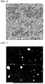
- the Ga-rich region is, for example, an area observed to be white in a COMPO image obtained by an EPMA, as shown in FIG. 5 .
- the average grain size of the ⁇ phase is obtained in the following manner.
- a surface of a sample cut out from the sputtering target is polished so as to become a mirror surface, and is etched by using an etchant which is formed from nitric acid and pure water.
- a microphotograph is captured by an optical microscope which can distinguish a crystal particle boundary at a magnification of a range from 50 times to 1000 times, and 10 straight lines for dividing one side of the obtained photograph into 11 equal parts are drawn.
- the number of crystal particles through which the 10 straight lines pass is calculated, and the average grain size of the ⁇ phase is obtained by the following calculation expression.
- Average grain size (value obtained by correcting lengths of the 10 straight lines on the photograph to be actual lengths)/(the number of crystal particles through which the 10 straight lines pass)
- the average grain size of the Na compound phases is measured based on an element distribution mapping image of Na obtained by the EPMA, as shown in FIG. 7 .
- a white area indicates the presence of Na and represents the size of the Na compound phase.
- An occupied area S ( ⁇ m 2 ) is measured and obtained by setting this white area as one Na compound particle.
- An average grain size (average value of D) and the maximum grain size (maximum value of D) are calculated from the number of Na compound particles observed in 10 square areas having one side of 100 ⁇ m, and grain sizes D.
- the oxygen content is measured by an infrared absorbing method which is described in "General rules for determination of oxygen in metallic materials" of JIS Z 2613.
- the method for producing a sputtering target in the present embodiment has a step of performing pressureless sintering by heating a molded body in a reducing atmosphere.
- the molded body is formed from a powder mixture of a pure Cu powder, a Cu-Ga alloy powder, and a Na compound.
- a pure Cu powder in which D50 measured by Microtrac is 2 ⁇ m to 3 ⁇ m, a Cu-Ga alloy atomized powder in which D50 is 20 ⁇ m to 30 ⁇ m, and aNa compound sieved to cause D50 to be 10 ⁇ m to 20 ⁇ m are weighed so as to be a target composition, and are mixed with each other in an Ar atmosphere by using a Henschel mixer to obtain a powder mixture.
- the Cu-Ga alloy atomized powder is manufactured in such a manner that a Cu-Ga alloy is dissolved in a gas-atomizing device so as to cause the concentration of Ga to be 50 atomic%, and is atomized by using an Ar gas.
- a green compact (molded body) is obtained at a molding pressure of 500 kgf/cm 2 to 2000 kgf/cm 2 by using the obtained powder mixture.
- the green compact is arranged in a furnace.
- a reducing gas is flowed at 10 L/min to 100 L/min, and the green compact is heated up to a sintering temperature of 700°C to 1000°C at 10°C/min and is held for 5 hours.
- the inside of the furnace is naturally cooled, and lathe work is performed on a surface portion and on an outer circumference portion of the obtained sintered body. Thereby, a sputtering target having a diameter of 50 mm and a thickness of 6 mm is manufactured.
- the processed sputtering target is hot pressed by using a Cu backing plate and is used in sputtering.
- the Cu-Ga alloy sputtering target manufactured in this manner is used in a direct-current (DC) magnetron sputtering device by using an Ar gas as a sputtering gas.
- DC direct-current
- the main peak intensity in X-ray diffraction attributed to the ⁇ phase is equal to or more than 5% of the main peak intensity in X-ray diffraction attributed to the ⁇ phase.
- the oxygen content is equal to or less than 200 mass ppm and the average grain size of the ⁇ phases of the Cu-Ga alloy is equal to or less than 100 ⁇ m.
- the Na compound phases having an average grain size which is equal to or less than 8.5 ⁇ m are dispersed and the maximum grain size thereof is suppressed so as to be equal to or less than 20 ⁇ m. Accordingly, the abnormal discharging is significantly reduced.
- An increase of an amount of oxygen in a precursor film obtained through sputtering is suppressed by significantly reducing the oxygen content and it is possible to contribute to improvement of photoelectric conversion efficiency in a light-absorbing layer of a CIGS thin-film solar cell.
- pressureless sintering is performed by heating the molded body formed from the powder mixture of the pure Cu powder, the Cu-Ga alloy powder, and the Na compound, in the reducing atmosphere.
- mutual diffusion occurs from the raw material powders thereof during sintering, and the ⁇ phase and the ⁇ phase appear as a metal phase in the sintered body.
- the sintered body in which an X-ray diffraction peak attributed to the ⁇ phase of the Cu-Ga alloy and an X-ray diffraction peak attributed to the ⁇ phase are observed, with extremely low oxygen content is obtained.
- the reason for two phases of the ⁇ phase and the ⁇ phase being present together is as follows. That is, a Ga-rich liquid phase appears from the Cu-Ga alloy powder, and so-called liquid phase sintering is performed in sintering. Thus, particles are easily rearranged and a high-density sintered body is obtained while a powder is sintered at normal pressure. In the process of cooling the sintered body, the sintered body is separated into the ⁇ phase and the ⁇ phase at the vicinity of 620°C. According to the Cu-Ga phase diagram (source of reference, Desk Handbook: Phase Diagrams for Binary Alloys (ASM International)) shown in FIG. 1 , it is expected that this phase separation necessarily occurs when an atom ratio of Ga is less than 30%.
- An advantage of coexistence of the two phases is that coarsening of a crystal particle in the ⁇ phase is suppressed by the presence of the ⁇ phase, the average grain size of a target structure becomes small, and the abnormal discharging during sputtering is less likely to occur.
- mixed powders of Examples 1 to 11 were prepared by blending the Cu-Ga alloy atomized powder (CuGa powder in the table), Ga concentration of which was 50 atomic%; the Cu powder; and the Na compound (NaF, Na 2 S, Na 2 Se, and Na 3 AlF 6 ), so as to have a weight ratio shown in Table 1.
- green compacts (molded body) were formed at the molding pressure of 1500kgf/cm 2 by using each of the obtained mixed powders.
- Examples 1 to 7 among the mixed powders were subjected to pressureless sintering in a hydrogen atmosphere.
- Examples 8 and 9 were subjected to pressureless sintering in a carbon monoxide atmosphere.
- Examples 10 and 11 were subjected to pressureless sintering in an atmosphere of an ammonia decomposition gas.
- the pressureless sintering was performed by holding the powder mixture at the sintering temperature of 840°C for 5 hours with a reducing gas flowing at 50 L/min.
- mixed powders of Comparative Examples 1 to 5 were prepared by blending the Cu-Ga alloy atomized powder (CuGa powder in the table), Ga concentration of which was 50 atomic%; the Cu powder; and the Na compound (NaF, Na 2 S, Na 2 Se, and Na 3 AlF 6 ), so as to have a weight ratio shown in Table 1.
- the Cu-Ga alloy powder was blended so as to cause the content of Ga to be out of range defined in the scope of the present invention.
- an excess of Na compound was blended.
- a green compacts (molded body) were formed by using each of the obtained mixed powders, similarly to the above-explained Examples.
- Comparative Example 1 among the mixed powders was subjected to pressureless sintering in an air atmosphere.
- Comparative Example 2 was sintered in a vacuum by using a hot pressing method. A condition of hot pressing was a holding time of 60 min at a holding temperature of 740°C.
- Comparative Examples 3 to 5 were subjected to pressureless sintering in a hydrogen atmosphere, similarly to the above-explained Examples.
- Example 1 Average grain size of ⁇ phase ( ⁇ m) Average grain size of Na compound ( ⁇ m) Maximum grain size of Na compound ( ⁇ m) X-ray diffraction Oxygen content (mass ppm) Abnormal discharge (times)
- Example 1 40 3.7 9.3 ⁇ , ⁇ 180 1
- Example 2 50 4.4 9.7 ⁇ , ⁇ 130 0
- Example 3 70 5.9 13.0 ⁇ , ⁇ 110 0
- Example 4 80 5.1 12.2 ⁇ , ⁇ 80 0
- Example 5 60 4.4 11.0 ⁇ , ⁇ 90 0
- Example 6 90 8.3 19.1 ⁇ , ⁇ 70 1
- Example 7 80 7.9 18.2 ⁇ , ⁇ 70 0
- Example 8 80 4.8 10.1 ⁇ , ⁇ 100 0
- Example 10 50 7.7 16.2 ⁇ , ⁇ 160 0
- Example 11 80 5.2 12.0 ⁇ , ⁇ 100 0
- Comparative Example 1 20 15.0 36.0 ⁇ , ⁇ 400 13 Comparative Example 2 20
- sputtering was performed under the following film formation condition for 12 hours and the number of occurrences of abnormal discharge was measured.
- the average grain size of the ⁇ phase was as small as 40 ⁇ m to 90 ⁇ m, and the two phases of the ⁇ phase and the ⁇ phase in X-ray diffraction were observed.
- the oxygen content was significantly low at 70 mass ppm to 180 mass ppm, and the average grain size and the maximum grain size of the Na compound phase were small.
- the number of occurrences of abnormal discharge was significantly reduced so as to be equal to or less than one time.
- the oxygen content was high as 400 mass ppm, and the number of occurrences of abnormal discharge was significantly increased to 13 times.
- the oxygen content was increased to 290 mass ppm and the number of occurrences of abnormal discharge was also significantly increased to 6 times.
- the oxygen content was increased to 350 mass ppm and the number of occurrences of abnormal discharge was also significantly increased to 5 times.
- Examples according to the present invention and Comparative Examples in which the content of Ga was set to 22.9 atomic%, 29.1 atomic%, and 30.4 atomic% were manufactured by performing pressureless sintering in which the sintered body was held at the sintering temperature of 840°C for 5 hours while flowing hydrogen gas at 50 L/min.
- Results obtained by measuring diffraction peaks of Examples and Comparative Examples through X-ray diffraction (XRD) are shown in FIGS. 2 to 4 .
- the sputtering target of Example 2 which contains 22.9 atomic% of Ga was manufactured by performing pressureless sintering in which the sintered body was held at the sintering temperature of 840°C for 5 hours while flowing hydrogen gas at 50 L/min.
- a compositional image (COMPO image) and an element-mapping image of Ga which were obtained by observing the obtained structure using the EPMA are shown in FIGS. 5 and 6 .
- the whitest portion indicates an area in which the content of Ga was high relatively to the sintered body.
- the original image of the element-mapping image of Ga is a color image, an image obtained by converting the original image into a monochrome image using a gray scale is shown. In the image, a portion having low brightness has a high Ga content.
- the examples according to the present invention have a crystal texture in which phases (Ga-rich region) having more Ga than the sintered body were dispersed.
- surface roughness be equal to or less than 1.5 ⁇ m
- an electrical resistance be equal to or less than 1 ⁇ 10 -4 ⁇ cm
- the amount of metal impurities be equal to or less than 0.1 atomic%
- a transverse strength be equal to or greater than 150 MPa. All of the examples satisfy these conditions.
- the sputtering targets of the embodiments and the examples have a plate-like shape.
- the sputtering target may have a cylindrical shape. More specifically, the sputtering target may have a disc plate-like shape, a short-side plate-like shape, a polygonal shape, and an elliptical plate-like shape, or a cylindrical shape.
Landscapes
- Chemical & Material Sciences (AREA)
- Engineering & Computer Science (AREA)
- Mechanical Engineering (AREA)
- Materials Engineering (AREA)
- Metallurgy (AREA)
- Organic Chemistry (AREA)
- Chemical Kinetics & Catalysis (AREA)
- Manufacturing & Machinery (AREA)
- Physics & Mathematics (AREA)
- Plasma & Fusion (AREA)
- Analytical Chemistry (AREA)
- Physical Vapour Deposition (AREA)
- Photovoltaic Devices (AREA)
- Powder Metallurgy (AREA)
Applications Claiming Priority (2)
| Application Number | Priority Date | Filing Date | Title |
|---|---|---|---|
| JP2013160134A JP6120076B2 (ja) | 2013-08-01 | 2013-08-01 | Cu−Ga合金スパッタリングターゲット及びその製造方法 |
| PCT/JP2014/069735 WO2015016153A1 (ja) | 2013-08-01 | 2014-07-25 | Cu-Ga合金スパッタリングターゲット及びその製造方法 |
Publications (2)
| Publication Number | Publication Date |
|---|---|
| EP3029171A1 true EP3029171A1 (de) | 2016-06-08 |
| EP3029171A4 EP3029171A4 (de) | 2017-03-29 |
Family
ID=52431688
Family Applications (1)
| Application Number | Title | Priority Date | Filing Date |
|---|---|---|---|
| EP14831218.4A Withdrawn EP3029171A4 (de) | 2013-08-01 | 2014-07-25 | Cu-ga-legierungssputtertarget und verfahren zur herstellung davon |
Country Status (6)
| Country | Link |
|---|---|
| US (1) | US10017850B2 (de) |
| EP (1) | EP3029171A4 (de) |
| JP (1) | JP6120076B2 (de) |
| CN (1) | CN105358733B (de) |
| TW (1) | TWI617681B (de) |
| WO (1) | WO2015016153A1 (de) |
Families Citing this family (8)
| Publication number | Priority date | Publication date | Assignee | Title |
|---|---|---|---|---|
| JP6147788B2 (ja) * | 2015-03-26 | 2017-06-14 | Jx金属株式会社 | Cu−Ga合金スパッタリングターゲット |
| JP6888294B2 (ja) * | 2016-02-03 | 2021-06-16 | 三菱マテリアル株式会社 | Cu−Ga合金スパッタリングターゲットの製造方法、及び、Cu−Ga合金スパッタリングターゲット |
| WO2017134999A1 (ja) * | 2016-02-03 | 2017-08-10 | 三菱マテリアル株式会社 | Cu-Ga合金スパッタリングターゲットの製造方法、及び、Cu-Ga合金スパッタリングターゲット |
| JP6794850B2 (ja) * | 2016-02-08 | 2020-12-02 | 三菱マテリアル株式会社 | スパッタリングターゲット及びスパッタリングターゲットの製造方法 |
| JP2019044222A (ja) * | 2017-08-31 | 2019-03-22 | 三菱マテリアル株式会社 | In−Cu合金粉末、In−Cu合金粉末の製造方法、In−Cu合金スパッタリングターゲット及びIn−Cu合金スパッタリングターゲットの製造方法 |
| JP6531816B1 (ja) | 2017-12-22 | 2019-06-19 | 三菱マテリアル株式会社 | Cu−Ga合金スパッタリングターゲット、及び、Cu−Ga合金スパッタリングターゲットの製造方法 |
| JP2019112671A (ja) * | 2017-12-22 | 2019-07-11 | 三菱マテリアル株式会社 | Cu−Ga合金スパッタリングターゲット、及び、Cu−Ga合金スパッタリングターゲットの製造方法 |
| JP2019183277A (ja) * | 2018-04-04 | 2019-10-24 | 三菱マテリアル株式会社 | Cu−Ga合金スパッタリングターゲット |
Citations (3)
| Publication number | Priority date | Publication date | Assignee | Title |
|---|---|---|---|---|
| US20120045360A1 (en) * | 2009-04-14 | 2012-02-23 | Kobelco Research Institute, Inc | Cu-ga alloy sputtering target and manufacturing method thereof |
| US20120217157A1 (en) * | 2009-11-06 | 2012-08-30 | Mitsubishi Materials Corporation | Sputtering target and method for producing the same |
| WO2012147985A1 (ja) * | 2011-04-29 | 2012-11-01 | 三菱マテリアル株式会社 | スパッタリングターゲット及びその製造方法 |
Family Cites Families (5)
| Publication number | Priority date | Publication date | Assignee | Title |
|---|---|---|---|---|
| JP3249408B2 (ja) | 1996-10-25 | 2002-01-21 | 昭和シェル石油株式会社 | 薄膜太陽電池の薄膜光吸収層の製造方法及び製造装置 |
| JP5202643B2 (ja) | 2009-07-23 | 2013-06-05 | Jx日鉱日石金属株式会社 | Cu−Ga合金焼結体スパッタリングターゲット及び同ターゲットの製造方法 |
| JP4831258B2 (ja) | 2010-03-18 | 2011-12-07 | 三菱マテリアル株式会社 | スパッタリングターゲット及びその製造方法 |
| JP2012017481A (ja) * | 2010-07-06 | 2012-01-26 | Mitsui Mining & Smelting Co Ltd | Cu−Ga合金およびCu−Ga合金スパッタリングターゲット |
| US7935558B1 (en) | 2010-10-19 | 2011-05-03 | Miasole | Sodium salt containing CIG targets, methods of making and methods of use thereof |
-
2013
- 2013-08-01 JP JP2013160134A patent/JP6120076B2/ja active Active
-
2014
- 2014-07-25 WO PCT/JP2014/069735 patent/WO2015016153A1/ja active Application Filing
- 2014-07-25 CN CN201480038680.4A patent/CN105358733B/zh active Active
- 2014-07-25 US US14/908,346 patent/US10017850B2/en active Active
- 2014-07-25 EP EP14831218.4A patent/EP3029171A4/de not_active Withdrawn
- 2014-07-29 TW TW103125861A patent/TWI617681B/zh active
Patent Citations (4)
| Publication number | Priority date | Publication date | Assignee | Title |
|---|---|---|---|---|
| US20120045360A1 (en) * | 2009-04-14 | 2012-02-23 | Kobelco Research Institute, Inc | Cu-ga alloy sputtering target and manufacturing method thereof |
| US20120217157A1 (en) * | 2009-11-06 | 2012-08-30 | Mitsubishi Materials Corporation | Sputtering target and method for producing the same |
| WO2012147985A1 (ja) * | 2011-04-29 | 2012-11-01 | 三菱マテリアル株式会社 | スパッタリングターゲット及びその製造方法 |
| US20140034491A1 (en) * | 2011-04-29 | 2014-02-06 | Mitsubishi Materials Corporation | Sputtering target and method for producing same |
Non-Patent Citations (1)
| Title |
|---|
| See also references of WO2015016153A1 * |
Also Published As
| Publication number | Publication date |
|---|---|
| TW201510250A (zh) | 2015-03-16 |
| WO2015016153A1 (ja) | 2015-02-05 |
| CN105358733A (zh) | 2016-02-24 |
| JP2015030870A (ja) | 2015-02-16 |
| JP6120076B2 (ja) | 2017-04-26 |
| EP3029171A4 (de) | 2017-03-29 |
| CN105358733B (zh) | 2018-01-26 |
| US20160208376A1 (en) | 2016-07-21 |
| TWI617681B (zh) | 2018-03-11 |
| US10017850B2 (en) | 2018-07-10 |
Similar Documents
| Publication | Publication Date | Title |
|---|---|---|
| US10017850B2 (en) | Cu—Ga alloy sputtering target, and method for producing same | |
| EP2703519B1 (de) | Sputtertarget und herstellungsverfahren dafür | |
| US20120286219A1 (en) | Sputtering target, semiconducting compound film, solar cell comprising semiconducting compound film, and method of producing semiconducting compound film | |
| EP2589571A1 (de) | Pulver, sinterkörper und sputtertarget, jedes mit den elementen cu, in, ga und se, sowie verfahren zur herstellung des pulvers | |
| KR20130028067A (ko) | 스퍼터링 타깃 및 그 제조 방법 | |
| WO2011083647A1 (ja) | Cu-Ga系スパッタリングターゲット、同ターゲットの製造方法、光吸収層及び該光吸収層を用いた太陽電池 | |
| JP5907428B2 (ja) | スパッタリングターゲット及びその製造方法 | |
| WO2013125716A1 (ja) | スパッタリングターゲット及びその製造方法 | |
| EP2500447A1 (de) | Quaternäres cu-in-ga-se-legierungs-sputtertarget | |
| KR20140097131A (ko) | 스퍼터링 타깃 및 그 제조 방법 | |
| CN105705674B (zh) | Cu-Ga合金溅射靶及其制造方法 | |
| WO2016031974A1 (ja) | Cu-Gaスパッタリングターゲット及びCu-Gaスパッタリングターゲットの製造方法 | |
| TW201610193A (zh) | Cu-Ga合金濺鍍靶及其製造方法 | |
| US9528181B2 (en) | Sputtering target and method for producing same | |
| WO2014069652A1 (ja) | スパッタリングターゲット及びその製造方法 | |
| JP2012246574A (ja) | スパッタリングターゲット及びその製造方法 | |
| JP6436006B2 (ja) | スパッタリングターゲット及びその製造方法 | |
| JP6274525B2 (ja) | CuSnスパッタリングターゲット及びその製造方法 | |
| WO2015052848A1 (ja) | スパッタリングターゲット及びその製造方法 | |
| CN110337508B (zh) | Cu-Ga合金溅射靶及Cu-Ga合金溅射靶的制造方法 | |
| EP3730670A1 (de) | Sputtertarget aus cu-ga-legierung und verfahren zur herstellung des sputtertargets aus einer cu-ga-legierung | |
| TWI586824B (zh) | Sputtering target and its manufacturing method |
Legal Events
| Date | Code | Title | Description |
|---|---|---|---|
| PUAI | Public reference made under article 153(3) epc to a published international application that has entered the european phase |
Free format text: ORIGINAL CODE: 0009012 |
|
| 17P | Request for examination filed |
Effective date: 20160126 |
|
| AK | Designated contracting states |
Kind code of ref document: A1 Designated state(s): AL AT BE BG CH CY CZ DE DK EE ES FI FR GB GR HR HU IE IS IT LI LT LU LV MC MK MT NL NO PL PT RO RS SE SI SK SM TR |
|
| AX | Request for extension of the european patent |
Extension state: BA ME |
|
| DAX | Request for extension of the european patent (deleted) | ||
| A4 | Supplementary search report drawn up and despatched |
Effective date: 20170228 |
|
| RIC1 | Information provided on ipc code assigned before grant |
Ipc: C22C 1/04 20060101ALI20170222BHEP Ipc: C22C 1/05 20060101ALI20170222BHEP Ipc: C22C 9/00 20060101ALI20170222BHEP Ipc: C23C 14/34 20060101AFI20170222BHEP |
|
| STAA | Information on the status of an ep patent application or granted ep patent |
Free format text: STATUS: EXAMINATION IS IN PROGRESS |
|
| 17Q | First examination report despatched |
Effective date: 20190426 |
|
| RAP1 | Party data changed (applicant data changed or rights of an application transferred) |
Owner name: MITSUBISHI MATERIALS CORPORATION |
|
| STAA | Information on the status of an ep patent application or granted ep patent |
Free format text: STATUS: EXAMINATION IS IN PROGRESS |
|
| STAA | Information on the status of an ep patent application or granted ep patent |
Free format text: STATUS: EXAMINATION IS IN PROGRESS |
|
| GRAP | Despatch of communication of intention to grant a patent |
Free format text: ORIGINAL CODE: EPIDOSNIGR1 |
|
| STAA | Information on the status of an ep patent application or granted ep patent |
Free format text: STATUS: GRANT OF PATENT IS INTENDED |
|
| RIC1 | Information provided on ipc code assigned before grant |
Ipc: H01J 37/34 20060101ALI20220502BHEP Ipc: C22C 32/00 20060101ALI20220502BHEP Ipc: C22C 9/00 20060101ALI20220502BHEP Ipc: C22C 1/05 20060101ALI20220502BHEP Ipc: C22C 1/04 20060101ALI20220502BHEP Ipc: C23C 14/34 20060101AFI20220502BHEP |
|
| INTG | Intention to grant announced |
Effective date: 20220607 |
|
| STAA | Information on the status of an ep patent application or granted ep patent |
Free format text: STATUS: THE APPLICATION IS DEEMED TO BE WITHDRAWN |
|
| 18D | Application deemed to be withdrawn |
Effective date: 20221018 |