EP2973693B1 - Capacitor with a dielectric between a via and a plate of the capacitor - Google Patents
Capacitor with a dielectric between a via and a plate of the capacitor Download PDFInfo
- Publication number
- EP2973693B1 EP2973693B1 EP14720314.5A EP14720314A EP2973693B1 EP 2973693 B1 EP2973693 B1 EP 2973693B1 EP 14720314 A EP14720314 A EP 14720314A EP 2973693 B1 EP2973693 B1 EP 2973693B1
- Authority
- EP
- European Patent Office
- Prior art keywords
- capacitor
- substrate
- dielectric
- plate
- inductor
- Prior art date
- Legal status (The legal status is an assumption and is not a legal conclusion. Google has not performed a legal analysis and makes no representation as to the accuracy of the status listed.)
- Not-in-force
Links
Images


Classifications
-
- H—ELECTRICITY
- H10—SEMICONDUCTOR DEVICES; ELECTRIC SOLID-STATE DEVICES NOT OTHERWISE PROVIDED FOR
- H10D—INORGANIC ELECTRIC SEMICONDUCTOR DEVICES
- H10D1/00—Resistors, capacitors or inductors
- H10D1/60—Capacitors
- H10D1/68—Capacitors having no potential barriers
-
- G—PHYSICS
- G06—COMPUTING OR CALCULATING; COUNTING
- G06F—ELECTRIC DIGITAL DATA PROCESSING
- G06F30/00—Computer-aided design [CAD]
- G06F30/30—Circuit design
- G06F30/39—Circuit design at the physical level
-
- H—ELECTRICITY
- H01—ELECTRIC ELEMENTS
- H01L—SEMICONDUCTOR DEVICES NOT COVERED BY CLASS H10
- H01L23/00—Details of semiconductor or other solid state devices
- H01L23/48—Arrangements for conducting electric current to or from the solid state body in operation, e.g. leads, terminal arrangements ; Selection of materials therefor
- H01L23/481—Internal lead connections, e.g. via connections, feedthrough structures
-
- H—ELECTRICITY
- H01—ELECTRIC ELEMENTS
- H01L—SEMICONDUCTOR DEVICES NOT COVERED BY CLASS H10
- H01L23/00—Details of semiconductor or other solid state devices
- H01L23/48—Arrangements for conducting electric current to or from the solid state body in operation, e.g. leads, terminal arrangements ; Selection of materials therefor
- H01L23/488—Arrangements for conducting electric current to or from the solid state body in operation, e.g. leads, terminal arrangements ; Selection of materials therefor consisting of soldered or bonded constructions
- H01L23/498—Leads, i.e. metallisations or lead-frames on insulating substrates, e.g. chip carriers
- H01L23/49822—Multilayer substrates
-
- H—ELECTRICITY
- H01—ELECTRIC ELEMENTS
- H01L—SEMICONDUCTOR DEVICES NOT COVERED BY CLASS H10
- H01L23/00—Details of semiconductor or other solid state devices
- H01L23/48—Arrangements for conducting electric current to or from the solid state body in operation, e.g. leads, terminal arrangements ; Selection of materials therefor
- H01L23/488—Arrangements for conducting electric current to or from the solid state body in operation, e.g. leads, terminal arrangements ; Selection of materials therefor consisting of soldered or bonded constructions
- H01L23/498—Leads, i.e. metallisations or lead-frames on insulating substrates, e.g. chip carriers
- H01L23/49827—Via connections through the substrates, e.g. pins going through the substrate, coaxial cables
-
- H—ELECTRICITY
- H10—SEMICONDUCTOR DEVICES; ELECTRIC SOLID-STATE DEVICES NOT OTHERWISE PROVIDED FOR
- H10D—INORGANIC ELECTRIC SEMICONDUCTOR DEVICES
- H10D1/00—Resistors, capacitors or inductors
- H10D1/20—Inductors
-
- H—ELECTRICITY
- H10—SEMICONDUCTOR DEVICES; ELECTRIC SOLID-STATE DEVICES NOT OTHERWISE PROVIDED FOR
- H10D—INORGANIC ELECTRIC SEMICONDUCTOR DEVICES
- H10D1/00—Resistors, capacitors or inductors
- H10D1/60—Capacitors
- H10D1/68—Capacitors having no potential barriers
- H10D1/692—Electrodes
-
- H—ELECTRICITY
- H10—SEMICONDUCTOR DEVICES; ELECTRIC SOLID-STATE DEVICES NOT OTHERWISE PROVIDED FOR
- H10D—INORGANIC ELECTRIC SEMICONDUCTOR DEVICES
- H10D86/00—Integrated devices formed in or on insulating or conducting substrates, e.g. formed in silicon-on-insulator [SOI] substrates or on stainless steel or glass substrates
- H10D86/80—Integrated devices formed in or on insulating or conducting substrates, e.g. formed in silicon-on-insulator [SOI] substrates or on stainless steel or glass substrates characterised by multiple passive components, e.g. resistors, capacitors or inductors
- H10D86/85—Integrated devices formed in or on insulating or conducting substrates, e.g. formed in silicon-on-insulator [SOI] substrates or on stainless steel or glass substrates characterised by multiple passive components, e.g. resistors, capacitors or inductors characterised by only passive components
-
- H—ELECTRICITY
- H01—ELECTRIC ELEMENTS
- H01L—SEMICONDUCTOR DEVICES NOT COVERED BY CLASS H10
- H01L23/00—Details of semiconductor or other solid state devices
- H01L23/12—Mountings, e.g. non-detachable insulating substrates
- H01L23/14—Mountings, e.g. non-detachable insulating substrates characterised by the material or its electrical properties
- H01L23/15—Ceramic or glass substrates
-
- H—ELECTRICITY
- H01—ELECTRIC ELEMENTS
- H01L—SEMICONDUCTOR DEVICES NOT COVERED BY CLASS H10
- H01L2924/00—Indexing scheme for arrangements or methods for connecting or disconnecting semiconductor or solid-state bodies as covered by H01L24/00
- H01L2924/0001—Technical content checked by a classifier
- H01L2924/0002—Not covered by any one of groups H01L24/00, H01L24/00 and H01L2224/00
-
- H—ELECTRICITY
- H10—SEMICONDUCTOR DEVICES; ELECTRIC SOLID-STATE DEVICES NOT OTHERWISE PROVIDED FOR
- H10D—INORGANIC ELECTRIC SEMICONDUCTOR DEVICES
- H10D86/00—Integrated devices formed in or on insulating or conducting substrates, e.g. formed in silicon-on-insulator [SOI] substrates or on stainless steel or glass substrates
Definitions
- the present disclosure is generally related to a capacitor.
- wireless computing devices such as portable wireless telephones, personal digital assistants (PDAs), and paging devices that are small, lightweight, and easily carried by users.
- portable wireless telephones such as cellular telephones and internet protocol (IP) telephones
- IP internet protocol
- wireless telephones may communicate voice and data packets over wireless networks.
- many such wireless telephones include other types of devices that are incorporated therein.
- a wireless telephone may also include a digital still camera, a digital video camera, a digital recorder, and an audio file player.
- such wireless telephones may process executable instructions, including software applications, such as a web browser application, that may be used to access the Internet. As such, these wireless telephones may include significant computing capabilities.
- a device for use in wireless communication devices may be formed using through-glass-via (TGV) technology to provide smaller size, higher performance, and cost advantages as compared to multi-layer chip diplexer (MLCD) technology.
- a device formed using TGV technology may include a circuit (e.g. a resonant circuit, such as an inductive-capacitive (L-C) resonator circuit) that may have a capacitor and an inductor.
- a circuit e.g. a resonant circuit, such as an inductive-capacitive (L-C) resonator circuit
- L-C inductive-capacitive
- An L-C resonator circuit using TGV technology involves fabrication of an inductor using a partially filled through-glass-via (TGV) structure and a capacitor coupled to the inductor via a metal trace that extends along a substrate from the TGV to the capacitor.
- the metal trace along the L-C resonator circuit introduces additional resistance, which may degrade overall circuit performance in terms of more power consumption.
- the increase in the series resistance decreases the quality factor (Q factor) of the resonator circuit, indicating a higher rate of energy loss (or power loss) relative to a stored energy of the circuit.
- JP 2002 008942 A relates to a decoupling capacitor connected between a power supply line and a ground line.
- DE 10 2008 003952 A1 relates to a microminiature inverter such as a DC-DC converter composed of a semiconductor element and passive components.
- a solid-filled (or hermetic-filled) via e.g., TGV
- TGV hermetic-filled via
- a circuit may have lower power consumption than by having a capacitor that is offset from the via and that is coupled to the via using a metal trace.
- the disclosed circuit may have a lower resistance by use of the capacitor positioned on the via. The reduced resistance may result in lower power consumption.
- the quality factor (Q factor) of the circuit may be higher than conventional circuits. The higher quality factor indicates a lower rate of energy loss relative to stored energy of the circuit.
- the disclosed circuit may have a smaller size by including the capacitor without the offset from the via.
- circuits that include a capacitor with a dielectric between a via and a plate of the capacitor and methods of fabricating circuits are presented in this disclosure. It should be appreciated, however, that the concepts and insights used in the particular embodiments with respect to designs of the circuits may be embodied in a variety of contexts. The particular embodiments presented are merely illustrative, and do not limit the scope of this disclosure.
- FIG. 1 a particular illustrative embodiment of a circuit including a capacitor with a dielectric between a via and a plate of the capacitor is disclosed.
- FIG. 1 shows a cross-sectional view of a portion of a device 100 that includes a circuit.
- the device 100 includes a bottom surface 190 and a top surface 192.
- the device 100 includes a substrate 102.
- the device 100 may include a first via 104 that extends through the substrate 102 from one side of the substrate 102 to the other side of the substrate 102.
- the device 100 also includes a capacitor 114.
- the capacitor 114 includes a dielectric 106 between the first via 104 and a second plate 108 of the capacitor 114.
- the substrate 102 may be made of a low-loss material (e.g., dielectric, wide-bandgap semiconductor, etc.).
- the low-loss material may include a dielectric material or a highly-insulative semiconductor material.
- the device 100 is a passive device
- the substrate 102 includes a glass-type substrate
- the first via 104 includes a through-glass via.
- the substrate 102 may include a glass substrate, a quartz substrate, a silicon-on-insulator (SOI) substrate, a silicon-on-sapphire (SOS) substrate, a high resitivity substrate (HRS), a gallium arsenide (GaAs) substrate, an indium phosphide (InP) substrate, a silicon carbide (SiC) substrate, an aluminum nitride (AIN) substrate, rogers laminates, or a plastic substrate, as illustrative, non-limiting examples.
- SOI silicon-on-insulator
- SOS silicon-on-sapphire
- HRS high resitivity substrate
- GaAs gallium arsenide
- InP indium phosphide
- SiC silicon carbide
- AIN aluminum nitride
- rogers laminates or a plastic substrate, as illustrative, non-limiting examples.
- the first via 104 may be filled with metal.
- the metal includes at least one of copper (Cu), tungsten (W), silver (Ag), or gold (Au).
- the capacitor 114 includes a second plate 108 (e.g., a second metal layer), the dielectric 106, and a first plate 120 (e.g., a first metal layer).
- the first plate 120 may be located between the first via 104 and the dielectric 106.
- the first plate 120 is electrically coupled to the first via 104.
- the first plate 120 and the second plate 108 are located within the device 100.
- the dielectric 106 may include at least one of silicon dioxide (SiO2), silicon nitride (Si3N4), silicon oxynitride (SiOxNy), tantalum pentoxide (Ta2O5), aluminum oxide (Al2O3), or aluminum nitride (AIN).
- the second plate 108 of the capacitor 114 is external to (e.g., above and not embedded within) the substrate 102.
- the device 100 may include an inductor that includes the first via 104, a first conductive structure 140 (e.g., a back-side metal layer), a second via 130, a second conductive structure 142 (e.g., a third metal layer), a third via 132, and a third conductive structure 144 (e.g., a back-side metal layer).
- a first conductive structure 140 e.g., a back-side metal layer
- second via 130 e.g., a second conductive structure 142 (e.g., a third metal layer)
- a third via 132 e.g., a back-side metal layer
- a third conductive structure 144 e.g., a back-side metal layer
- the first conductive structure 140 and the third conductive structure 144 may be located in a first inter-layer dielectric (ILD) 110 to electrically insulate the first conductive structure 140 and the third conductive structure 144 from other devices or circuitry.
- the capacitor 114 and the second conductive structure 142 may be located in a second ILD 112 to electrically insulate the capacitor 114 and the second conductive structure 142 from other devices or circuitry.
- the second plate 108 may be located between a fourth conductive structure 146 (e.g., a third metal layer) and the dielectric 106.
- the fourth conductive structure 146 may be located in a passivation layer 150 to electrically insulate the fourth conductive structure 146 from other devices or circuitry.
- the inductor and the capacitor 114 may form a resonant circuit. For example, when the capacitor 114 is charged with a first polarity and begins to discharge, an electric current may begin flowing through the inductor. While the capacitor 114 discharges, a magnetic field of the inductor may build as a result of the electric current flowing through the inductor. After the capacitor 114 has discharged, the magnetic field may cause the capacitor 114 to charge with an opposite polarity to the first polarity as flow of the electric current through the inductor reduces. A second electric current in an opposite direction of the electric current may then begin flowing through the inductor as a strength of the magnetic field is reduced. The second electric current may discharge the capacitor 114 and then recharge the capacitor 114 with the earlier polarity.
- Voltage across the capacitor 114 and the inductor may oscillate at a frequency (e.g., a resonant frequency) approximately equal to a capacitance value of the capacitor 114 multiplied by an inductance value of the inductor. Losses in current due to resistance may dampen oscillations and may reduce efficiency of the circuit.
- the first circuit of the device 100 may have lower power consumption than by having a capacitor 114 that is not positioned above the first via 104.
- the first circuit may have a lower resistance by use of the capacitor 114 without added resistance from a metal line connecting the first via 104 to the capacitor 114.
- the reduced resistance may result in lower power consumption during use of the first circuit.
- the quality factor (Q factor) of the first circuit may be higher than conventional circuits. The higher quality factor indicates a lower rate of energy loss relative to stored energy of the first circuit.
- the first circuit may have a smaller size by including the capacitor 114 above, rather than beside (or offset from), the first via 104.
- film deposition processes such as chemical vapor deposition (CVD), physical vapor deposition (PVD) (e.g., sputtering or evaporation), and/or electroplating may be used to form metal layers and inter-metal dielectric layers.
- CVD chemical vapor deposition
- PVD physical vapor deposition
- electroplating may be used to form metal layers and inter-metal dielectric layers.
- Photolithography may be used to form patterns of metal layers.
- An etching process may be performed to remove unwanted materials.
- Planarization processes such as "etch-back” and chemical-mechanical polishing (CMP) may be employed to create a flat surface.
- the device 100 may host a number of connectors, inductors, layers, and other structures or devices.
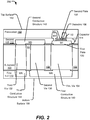
- FIG. 2 shows a cross-sectional view of a portion of a device 200 that includes a second circuit.
- the device 200 includes the substrate 102 and the first via 104.
- the device 200 may also include the capacitor 114.
- the capacitor 114 includes the dielectric 106 between the first via 104 and the second plate 108 of the capacitor 114.
- a surface of the first via 104 facing the dielectric 106 may be larger than a surface of the second plate 108.
- a top surface of the first via 104 may be larger than a bottom surface of the second plate 108.
- the surface of the first via 104 may be a same size as a surface of the second plate 108 of the capacitor 114.
- the top surface of the first via 104 may be the same size as the bottom surface of the second plate 108.
- the surface of the first via 104 may be smaller than a surface of the second plate 108 of the capacitor 114.
- the top surface of the first via 104 may be smaller than the bottom surface of the second plate 108.
- the surface of the first via 104 facing the dielectric 106 being larger than the second plate 108 corresponds to use of a larger first via 104.
- Use of a larger first via 104 reduces resistance of the second circuit.
- the quality factor of the second circuit is increased.
- a higher quality factor indicates a lower rate of energy loss relative to stored energy of the second circuit.
- FIG. 3 shows a cross-sectional view of a portion of a device 300 that includes a third circuit.
- the device 300 includes the substrate 102 and the first via 104.
- the device 300 may also include the capacitor 114.
- the capacitor 114 includes the dielectric 106 between the first via 104 and the second plate 108 of the capacitor 114.
- the first via 104 in FIG. 3 may include a metal structure 304 with a polymer core 302.
- the metal structure may include at least one of copper (Cu), tungsten (W), silver (Ag), or gold (Au).
- the polymer core may include at least one of polyimide (PI), benzocyclobutene (BCB), acrylic, polybenzoxazole (PBO), or photoresist (e.g., TMMR®, SU-8, or other types of photoresists).
- PI polyimide
- BCB benzocyclobutene
- PBO polybenzoxazole
- photoresist e.g., TMMR®, SU-8, or other types of photoresists.
- Having a polymer core 302 may enable the first via 104 to provide structural support to the capacitor 114 and may be more compatible with TGV fabrication techniques than completely filling the first via 104 with metal.
- having the polymer core 302 may reduce a material cost of the first via 104, e.g., polymer materials may cost less than metal.
- FIG. 4 shows a cross-sectional view of a portion of a device 400 that includes a fourth circuit.
- the device 400 includes the substrate 102 and the first via 104.
- the device 400 may also include a capacitor 414.
- the capacitor 414 includes the dielectric 106 between the first via 104 and the second plate 108 of the capacitor 414.
- the first via 104 forms a plate of the capacitor 414 and may function as a bottom plate of the capacitor 414.
- the device 400 may include a second dielectric 402 between the first via 104 and the dielectric 106.
- Having the first via 104 function as the bottom plate of the capacitor 414 may reduce a resistance of the fourth circuit as compared to the second circuit of FIG. 2 with the capacitor 114 having the first plate 120 function as the bottom plate. As a result, the quality factor of the fourth circuit may improve, indicating a lower rate of energy loss relative to a stored energy of the fourth circuit.
- forming the device 400 may involve fewer lithography stages where the first via 104 functions as the bottom plate of the capacitor 414, as compared to forming the device 200 that may include the first plate 120 (e.g., a first metal layer). Having the first via 104 function as the bottom plate of the capacitor 414 may also reduce a height of the device 400 as compared to the device 200.
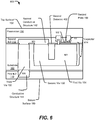
- FIG. 5 shows a cross-sectional view of a portion of a wafer that includes a fifth circuit.
- the device 500 includes the substrate 102 and the first via 104.
- the device 500 may also include a capacitor 514.
- the capacitor 514 in FIG. 5 includes a single dielectric layer (i.e., the second dielectric 402) between the first via 104 and the second plate 108 of the capacitor 514.
- the second dielectric 402 may include at least one of silicon dioxide (SiO2), silicon nitride (Si3N4), silicon oxynitride (SiOxNy), tantalum pentoxide (Ta2O5), aluminum oxide (Al2O3), or aluminum nitride (AlN).
- Having a single dielectric layer (i.e., the second dielectric 402) between the first via 104 and the second plate 108 of the capacitor 514 may reduce a number of lithography stages of forming the device 500, as compared to the device 400 of FIG. 4 with multiple dielectric layers (i.e., the dielectric 106 and the second dielectric 402). As a result, the complexity and cost of fabricating the device 500 may be lower than of fabricating the device 400.
- FIG. 6 shows a cross-sectional view of a portion of a device 600 that includes a sixth circuit.
- the device 600 includes the substrate 102 and the first via 104.
- the device 600 may also include a capacitor 614.
- the capacitor 614 includes the second dielectric 402 between the first via 104 and the second plate 108 of the capacitor 614.
- the first via 104 may extend partially through the substrate 102 and the second via 130 may extend partially through the substrate 102.
- the first via 104 and the second via 130 may be blind vias that are coupled within the substrate 102 and that do not extend from one side of the substrate 102 to the other side of the substrate 102.
- the first via 104 and the second via 130 may be joined within the substrate 102.
- Having the first via 104 and the second via 130 coupled within the substrate 102 may reduce a resistance of the sixth circuit, such as when a resistance between the first via 104 and the second via 130 is less than a resistance of the first conductive structure 140 coupling the first via 104 and the second via 130 of FIG. 5 .
- a quality factor of the sixth circuit may improve, indicating a lower rate of energy loss relative to a stored energy of the sixth circuit.
- FIG. 7 a flow chart of a particular illustrative embodiment of a method of forming a circuit including a capacitor having a dielectric between a via and a plate of the capacitor is depicted and generally designated 700.
- the method 700 includes forming a via that extends at least partially through a substrate of a device, at 702.
- the first via 104 may extend at least partially through the substrate 102.
- forming the first via 104 may include performing an anisotropic etch process on the substrate 102.
- the first via 104 may be formed using a slant via formation process, such as the first via 104 of FIG. 6 .
- the first via 104 may be filled with a metal, such as the first via 104 of FIGS. 1-2 and 4-6 .
- the first via 104 may be filled with a metal and a polymer, such as the first via 104 of FIG. 3 .
- the first via 104 may be filled using film deposition processes, such as electroplating, physical vapor deposition (PVD) (e.g., sputtering or evaporation), or chemical vapor deposition (CVD).
- PVD physical vapor deposition
- CVD chemical vapor deposition
- a conductive paste e.g., a paste including copper (Cu), tungsten (W), silver (Ag), or gold (Au)
- a planarization process may be used to remove unwanted or excess materials and to create a flat surface for subsequent processing.
- the planarization process may include chemical-mechanical polish (CMP).
- the planarization process may include an etch-back planarization process.
- the method 700 also includes forming a capacitor, at 704, that includes a dielectric between the via and a plate of the capacitor.
- the plate of the capacitor is external to the substrate and within the device.
- the capacitor may correspond to the capacitor 114 of FIGS. 1-3 , the capacitor 414 of FIG. 4 , the capacitor 514 of FIG. 5 , or the capacitor 614 of FIG. 6 .
- the capacitor may include the dielectric 106 of FIG. 1-4 , the second dielectric 402 of FIG. 4 , or both.
- the second plate 108 is external to the substrate 102 and within the device.
- the second plate 108 is within the device 100 of FIG. 1 , the device 200 of FIG. 2 , the device 300 of FIG. 3 , the device 400 of FIG. 4 , the device 500 of FIG. 5 , or the device 600 of FIG. 6 .
- the method of FIG. 7 may be implemented by a field-programmable gate array (FPGA) device, an application-specific integrated circuit (ASIC), a processing unit such as a central processing unit (CPU), a digital signal processor (DSP), a controller, another hardware device, firmware device, or any combination thereof.
- FPGA field-programmable gate array
- ASIC application-specific integrated circuit
- CPU central processing unit
- DSP digital signal processor
- the method 700 of FIG. 7 may be performed by a processor that executes instructions, as described with respect to FIG. 8 .
- the method 700 of FIG. 7 may be performed by fabrication equipment, such as a processor that executes instructions stored at a memory (e.g., a non-transitory computer-readable medium), as described further with reference to FIG. 9 .
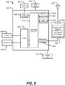
- the device 800 includes a processor 810, such as a digital signal processor (DSP), coupled to a memory 832 (e.g., a random access memory (RAM), flash memory, read-only memory (ROM), programmable read-only memory (PROM), erasable programmable read-only memory (EPROM), electrically erasable programmable read-only memory (EEPROM), registers, hard disk, a removable disk, a compact disc read-only memory (CD-ROM), or any other form of non-transient storage medium known in the art).
- the memory 832 may store instructions 862 executable by the processor 810.
- the memory 832 may store data 866 accessible to the processor 810.
- the device 800 includes a capacitor 864 with a dielectric between a via and a plate of the capacitor.
- the capacitor 864 may correspond to the capacitor 114 of FIGS. 1-3 , the capacitor 414 of FIG. 4 , the capacitor 514 of FIG. 5 , the capacitor 614 of FIG. 6 , a capacitor formed according to the method 700 of FIG. 7 , or a combination thereof.
- a radio frequency (RF) interface 852 may include the capacitor 864.
- FIG. 8 also shows a display controller 826 that is coupled to the processor 810 and to a display 828.
- a coder/decoder (CODEC) 834 may also be coupled to the processor 810.
- a speaker 836 and a microphone 838 may be coupled to the CODEC 834.
- FIG. 8 also indicates that a wireless controller 840 may be coupled to the processor 810 and may be further coupled to a wireless antenna 842 via the RF interface 852.
- the processor 810, the display controller 826, the memory 832, the CODEC 834, and the wireless controller 840 are included in a system-in-package or system-on-chip device 822.
- an input device 830 and a power supply 844 are coupled to the system-on-chip device 822.
- the display 828, the input device 830, the speaker 836, the microphone 838, the wireless antenna 842, and the power supply 844 are external to the system-on-chip device 822.
- each of the display 828, the input device 830, the speaker 836, the microphone 838, the wireless antenna 842, and the power supply 844 may be coupled to a component of the system-on-chip device 822, such as an interface or a controller.
- the foregoing disclosed devices and functionalities may be designed and configured into computer files (e.g. RTL, GDSII, GERBER, etc.) stored on computer readable media. Some or all such files may be provided to fabrication handlers who fabricate devices based on such files. Resulting products include wafers that are then cut into die and packaged into a chip. The chips are then integrated into electronic devices, as described further with reference to FIG. 9 .
- computer files e.g. RTL, GDSII, GERBER, etc.
- the physical device information 902 is received at the manufacturing process 900, such as at a research computer 906.
- the physical device information 902 may include design information representing at least one physical property of a device, such as a capacitor with a dielectric between a via and a plate of the capacitor (e.g., the capacitor 114 of FIGS. 1-3 , the capacitor 414 of FIG. 4 , the capacitor 514 of FIG. 5 , the capacitor 614 of FIG. 6 , and/or a capacitor formed according to the method 700 of FIG. 7 ).
- the physical device information 902 may include physical parameters, material characteristics, and structure information that is entered via a user interface 904 coupled to the research computer 906.
- the research computer 906 includes a processor 908, such as one or more processing cores, coupled to a computer readable medium such as a memory 910.
- the memory 910 may store computer readable instructions that are executable to cause the processor 908 to transform the physical device information 902 to comply with a file format and to generate a library file 912.
- the library file 912 includes at least one data file including the transformed design information.
- the library file 912 may include a library of circuits including a capacitor (e.g., the capacitor 114 of FIGS. 1-3 , the capacitor 414 of FIG. 4 , the capacitor 514 of FIG. 5 , the capacitor 614 of FIG. 6 , and/or a capacitor formed according to the method 700 of FIG. 7 ) provided for use with an electronic design automation (EDA) tool 920.
- EDA electronic design automation
- the library file 912 may be used in conjunction with the EDA tool 920 at a design computer 914 including a processor 916, such as one or more processing cores, coupled to a memory 918.
- the EDA tool 920 may be stored as processor executable instructions at the memory 918 to enable a user of the design computer 914 to design a circuit including the device (e.g., the capacitor 114 of FIGS. 1-3 , the capacitor 414 of FIG. 4 , the capacitor 514 of FIG. 5 , the capacitor 614 of FIG. 6 , and/or a capacitor formed according to the method 700 of FIG. 7 ) using the library file 912.
- a user of the design computer 914 may enter circuit design information 922 via a user interface 924 coupled to the design computer 914.
- the circuit design information 922 may include design information representing at least one physical property of a circuit (e.g., the capacitor 114 of FIGS. 1-3 , the capacitor 414 of FIG. 4 , the capacitor 514 of FIG. 5 , the capacitor 614 of FIG. 6 , and/or a capacitor formed according to the method 700 of FIG. 7 ).
- the circuit design property may include identification of particular circuits and relationships to other elements in a circuit design, positioning information, feature size information, interconnection information, or other information representing a physical property of a device.
- the design computer 914 may be configured to transform the design information, including the circuit design information 922, to comply with a file format.
- the file formation may include a database binary file format representing planar geometric shapes, text labels, and other information about a circuit layout in a hierarchical format, such as a Graphic Data System (GDSII) file format.
- the design computer 914 may be configured to generate a data file including the transformed design information, such as a GDSII file 926 that includes information describing a capacitor (e.g., the capacitor 114 of FIGS. 1-3 , the capacitor 414 of FIG. 4 , the capacitor 514 of FIG. 5 , the capacitor 614 of FIG. 6 , and/or a capacitor formed according to the method 700 of FIG.
- a capacitor e.g., the capacitor 114 of FIGS. 1-3 , the capacitor 414 of FIG. 4 , the capacitor 514 of FIG. 5 , the capacitor 614 of FIG. 6 , and/or a capacitor formed according to the method 700 of
- the data file may include information corresponding to a system-on-chip (SOC) that includes a capacitor (e.g., the capacitor 114 of FIGS. 1-3 , the capacitor 414 of FIG. 4 , the capacitor 514 of FIG. 5 , the capacitor 614 of FIG. 6 , and/or a capacitor formed according to the method 700 of FIG. 7 ), and that also includes additional electronic circuits and components within the SOC.
- SOC system-on-chip
- the GDSII file 926 may be received at a fabrication process 928 to manufacture a capacitor (e.g., the capacitor 114 of FIGS. 1-3 , the capacitor 414 of FIG. 4 , the capacitor 514 of FIG. 5 , the capacitor 614 of FIG. 6 , and/or a capacitor formed according to the method 700 of FIG. 7 ), according to transformed information in the GDSII file 926.
- a device manufacture process may include providing the GDSII file 926 to a mask manufacturer 930 to create one or more masks, such as masks to be used with photolithography processing, illustrated as a representative mask 932.
- the mask 932 may be used during the fabrication process to generate one or more wafers 934, which may be tested and separated into dies, such as a representative die 936.
- the die 936 includes a capacitor (e.g., the capacitor 114 of FIGS. 1-3 , the capacitor 414 of FIG. 4 , the capacitor 514 of FIG. 5 , the capacitor 614 of FIG. 6 , and/or a capacitor formed according to the method 700 of FIG. 7 ).
- a non-transitory computer-readable medium stores instructions executable by a computer to perform the method 700 of FIG. 7 .
- equipment of a manufacturing plant may include the computer and the memory and may perform the method 700 of FIG. 7 , such as in connection with the fabrication process 928 and using the GSDII file 926.
- the computer may execute instructions to initiate forming a via that extends at least partially through a substrate and forming a capacitor, as described with reference to FIG. 7 .
- the die 936 may be provided to a packaging process 938 where the die 936 is incorporated into a representative package 940.
- the package 940 may include the single die 936 or multiple dies, such as a system-in-package (SiP) arrangement.
- the package 940 may be configured to conform to one or more standards or specifications, such as Joint Electron Device Engineering Council (JEDEC) standards.
- JEDEC Joint Electron Device Engineering Council
- Information regarding the package 940 may be distributed to various product designers, such as via a component library stored at a computer 946.
- the computer 946 may include a processor 948, such as one or more processing cores, coupled to a memory 950.
- a printed circuit board (PCB) tool may be stored as processor executable instructions at the memory 950 to process PCB design information 942 received from a user of the computer 946 via a user interface 944.
- the PCB design information 942 may include physical positioning information of a packaged device on a circuit board, the packaged device corresponding to the package 940 including a capacitor (e.g., the capacitor 114 of FIGS. 1-3 , the capacitor 414 of FIG. 4 , the capacitor 514 of FIG. 5 , the capacitor 614 of FIG. 6 , and/or a capacitor formed according to the method 700 of FIG. 7 ).
- the computer 946 may be configured to transform the PCB design information 942 to generate a data file, such as a GERBER file 952 with data that includes physical positioning information of a packaged device on a circuit board, as well as layout of electrical connections such as traces and vias, where the packaged device corresponds to the package 940 including a capacitor (e.g., the capacitor 114 of FIGS. 1-3 , the capacitor 414 of FIG. 4 , the capacitor 514 of FIG. 5 , the capacitor 614 of FIG. 6 , and/or a capacitor formed according to the method 700 of FIG. 7 ).
- the data file generated by the transformed PCB design information may have a format other than a GERBER format.
- the GERBER file 952 may be received at a board assembly process 954 and used to create PCBs, such as a representative PCB 956, manufactured in accordance with the design information stored within the GERBER file 952.
- the GERBER file 952 may be uploaded to one or more machines to perform various steps of a PCB production process.
- the PCB 956 may be populated with electronic components including the package 940 to form a representative printed circuit assembly (PCA) 958.
- PCA printed circuit assembly
- the PCA 958 may be received at a product manufacture process 960 and integrated into one or more electronic devices, such as a first representative electronic device 962 and a second representative electronic device 964.
- the first representative electronic device 962, the second representative electronic device 964, or both may be selected from the group of a cellular phone, a wireless local area network (LAN) device, a set top box, a music player, a video player, an entertainment unit, a navigation device, a communications device, a personal digital assistant (PDA), a fixed location data unit, and a computer, into which a capacitor (e.g., the capacitor 114 of FIGS. 1-3 , the capacitor 414 of FIG. 4 , the capacitor 514 of FIG.
- a capacitor e.g., the capacitor 114 of FIGS. 1-3 , the capacitor 414 of FIG. 4 , the capacitor 514 of FIG.
- one or more of the electronic devices 962 and 964 may be remote units such as mobile phones, hand-held personal communication systems (PCS) units, portable data units such as personal data assistants, global positioning system (GPS) enabled devices, navigation devices, fixed location data units such as meter reading equipment, or any other device that stores or retrieves data or computer instructions, or any combination thereof.
- PCS personal communication systems
- GPS global positioning system
- FIG. 8 illustrates remote units according to teachings of the disclosure, the disclosure is not limited to these illustrated units. Embodiments of the disclosure may be suitably employed in any device which includes active integrated circuitry including memory and on-chip circuitry.
- a device that includes a capacitor may be fabricated, processed, and incorporated into an electronic device, as described in the illustrative process 900.
- a capacitor e.g., the capacitor 114 of FIGS. 1-3 , the capacitor 414 of FIG. 4 , the capacitor 514 of FIG. 5 , the capacitor 614 of FIG. 6 , and/or a capacitor formed according to the method 700 of FIG. 7
- a capacitor may be fabricated, processed, and incorporated into an electronic device, as described in the illustrative process 900.
- 1-9 may be included at various processing stages, such as within the library file 912, the GDSII file 926, and the GERBER file 952, as well as stored at the memory 910 of the research computer 906, the memory 918 of the design computer 914, the memory 950 of the computer 946, the memory of one or more other computers or processors (not shown) used at the various stages, such as at the board assembly process 954, and also incorporated into one or more other physical embodiments such as the mask 932, the die 936, the package 940, the PCA 958, other products such as prototype circuits or devices (not shown), or any combination thereof.
- FIGS. 1-9 various representative stages are depicted with reference to FIGS. 1-9 , in other embodiments fewer stages may be used or additional stages may be included.
- the process 900 of FIG. 9 may be performed by a single entity or by one or more entities performing various stages of the process 900.
- an apparatus in conjunction with the described embodiments, includes means for storing charge.
- the means for storing charge may include the capacitor of FIGS. 1-6 .
- the means for storing charge may include a dielectric.
- the dielectric may include the dielectric 106 of FIG. 1 , the second dielectric 402 of FIG. 4 , or a combination thereof.
- the apparatus also includes means for conducting current.
- the means for conducting current may extend at least partially through a substrate.
- the dielectric may be located between the means for conducting current and a plate of the means for storing charge.
- the plate may be external to the substrate and within the apparatus.
- the means for conducting current may include a via, such as the first via 104 of any of FIGs. 1-6 .
- a software module may reside in random access memory (RAM), flash memory, read-only memory (ROM), programmable read-only memory (PROM), erasable programmable read-only memory (EPROM), electrically erasable programmable read-only memory (EEPROM), registers, hard disk, a removable disk, a compact disc read-only memory (CD-ROM), or any other form of non-transient storage medium known in the art.
- An exemplary storage medium is coupled to the processor such that the processor may read information from, and write information to, the storage medium.
- the storage medium may be integral to the processor.
- the processor and the storage medium may reside in an application-specific integrated circuit (ASIC).
- ASIC application-specific integrated circuit
- the ASIC may reside in a computing device or a user terminal.
- the processor and the storage medium may reside as discrete components in a computing device or user terminal.
Landscapes
- Engineering & Computer Science (AREA)
- Computer Hardware Design (AREA)
- Physics & Mathematics (AREA)
- General Physics & Mathematics (AREA)
- Power Engineering (AREA)
- Condensed Matter Physics & Semiconductors (AREA)
- Microelectronics & Electronic Packaging (AREA)
- Theoretical Computer Science (AREA)
- Geometry (AREA)
- General Engineering & Computer Science (AREA)
- Evolutionary Computation (AREA)
- Semiconductor Integrated Circuits (AREA)
- Chemical & Material Sciences (AREA)
- Ceramic Engineering (AREA)
- Parts Printed On Printed Circuit Boards (AREA)
- Ceramic Capacitors (AREA)
- Fixed Capacitors And Capacitor Manufacturing Machines (AREA)
- Printing Elements For Providing Electric Connections Between Printed Circuits (AREA)
- Semiconductor Memories (AREA)
Applications Claiming Priority (2)
| Application Number | Priority Date | Filing Date | Title |
|---|---|---|---|
| US13/833,632 US9935166B2 (en) | 2013-03-15 | 2013-03-15 | Capacitor with a dielectric between a via and a plate of the capacitor |
| PCT/US2014/024118 WO2014150747A1 (en) | 2013-03-15 | 2014-03-12 | Capacitor with a dielectric between a via and a plate of the capacitor |
Publications (2)
| Publication Number | Publication Date |
|---|---|
| EP2973693A1 EP2973693A1 (en) | 2016-01-20 |
| EP2973693B1 true EP2973693B1 (en) | 2020-08-26 |
Family
ID=50625088
Family Applications (1)
| Application Number | Title | Priority Date | Filing Date |
|---|---|---|---|
| EP14720314.5A Not-in-force EP2973693B1 (en) | 2013-03-15 | 2014-03-12 | Capacitor with a dielectric between a via and a plate of the capacitor |
Country Status (6)
| Country | Link |
|---|---|
| US (1) | US9935166B2 (enExample) |
| EP (1) | EP2973693B1 (enExample) |
| JP (1) | JP2016518702A (enExample) |
| KR (1) | KR20150130516A (enExample) |
| CN (1) | CN105009280B (enExample) |
| WO (1) | WO2014150747A1 (enExample) |
Families Citing this family (19)
| Publication number | Priority date | Publication date | Assignee | Title |
|---|---|---|---|---|
| US9203373B2 (en) | 2013-01-11 | 2015-12-01 | Qualcomm Incorporated | Diplexer design using through glass via technology |
| US9634640B2 (en) | 2013-05-06 | 2017-04-25 | Qualcomm Incorporated | Tunable diplexers in three-dimensional (3D) integrated circuits (IC) (3DIC) and related components and methods |
| US9267653B2 (en) | 2013-05-16 | 2016-02-23 | Mckeon Products, Inc. | Light fixture with communication or power connector |
| US10480774B2 (en) | 2013-05-16 | 2019-11-19 | Mckeon Products, Inc. | Light emitter with communication or power connector |
| US9264013B2 (en) | 2013-06-04 | 2016-02-16 | Qualcomm Incorporated | Systems for reducing magnetic coupling in integrated circuits (ICS), and related components and methods |
| JP6657609B2 (ja) * | 2015-06-12 | 2020-03-04 | 凸版印刷株式会社 | 配線回路基板、半導体装置、配線回路基板の製造方法および半導体装置の製造方法 |
| US9954267B2 (en) | 2015-12-28 | 2018-04-24 | Qualcomm Incorporated | Multiplexer design using a 2D passive on glass filter integrated with a 3D through glass via filter |
| US10373868B2 (en) * | 2016-01-18 | 2019-08-06 | Infineon Technologies Austria Ag | Method of processing a porous conductive structure in connection to an electronic component on a substrate |
| JP6857329B2 (ja) * | 2016-10-24 | 2021-04-14 | 大日本印刷株式会社 | 高周波部品及びその製造方法 |
| JP6889399B2 (ja) * | 2017-08-08 | 2021-06-18 | 大日本印刷株式会社 | 貫通電極基板 |
| WO2019059898A1 (en) * | 2017-09-20 | 2019-03-28 | Intel Corporation | PERIPHERAL INDUCERS |
| JP2019102733A (ja) * | 2017-12-06 | 2019-06-24 | 凸版印刷株式会社 | 配線基板、半導体装置、及び配線基板の製造方法 |
| TWI669997B (zh) * | 2018-01-25 | 2019-08-21 | 欣興電子股份有限公司 | 線路板結構及其製作方法 |
| KR102609518B1 (ko) | 2018-09-21 | 2023-12-05 | 삼성전자주식회사 | 반도체 소자 형성 방법 |
| IT202000017554A1 (it) * | 2020-07-20 | 2022-01-20 | Thales Alenia Space Italia Spa Con Unico Socio | Feedthrough capacitivo per moduli ermetici ibridi |
| WO2022222131A1 (zh) * | 2021-04-23 | 2022-10-27 | 京东方科技集团股份有限公司 | 集成有无源器件的基板及其制备方法 |
| US20220375865A1 (en) * | 2021-05-18 | 2022-11-24 | Intel Corporation | Microelectronic assemblies with glass substrates and magnetic core inductors |
| US20220407212A1 (en) * | 2021-06-17 | 2022-12-22 | Intel Corporation | Millimeter wave components in a glass core of a substrate |
| CN114400286B (zh) * | 2022-01-14 | 2023-04-07 | 成都海威华芯科技有限公司 | 一种高可靠性通孔电容和制作方法 |
Family Cites Families (66)
| Publication number | Priority date | Publication date | Assignee | Title |
|---|---|---|---|---|
| US2757320A (en) | 1953-10-15 | 1956-07-31 | Westinghouse Electric Corp | Frequency sensitive control device |
| US3656162A (en) | 1969-09-19 | 1972-04-11 | Litton Systems Inc | Diplexer for radio communication |
| JPS5291446U (enExample) | 1975-12-29 | 1977-07-08 | ||
| US5404118A (en) | 1992-07-27 | 1995-04-04 | Murata Manufacturing Co., Ltd. | Band pass filter with resonator having spiral electrodes formed of coil electrodes on plurality of dielectric layers |
| JP3139327B2 (ja) | 1995-05-31 | 2001-02-26 | 株式会社村田製作所 | 高周波複合部品 |
| US5548255A (en) | 1995-06-23 | 1996-08-20 | Microphase Corporation | Compact diplexer connection circuit |
| JPH0992539A (ja) | 1995-09-22 | 1997-04-04 | Uniden Corp | 立体渦巻状インダクタ及びそれを用いた誘導結合フィルタ |
| JP3106942B2 (ja) | 1995-12-28 | 2000-11-06 | 株式会社村田製作所 | Lc共振部品 |
| US6366564B1 (en) | 1996-09-26 | 2002-04-02 | Matsushita Electric Industrial Co., Ltd. | Diplexer duplexer and two-channel mobile communications equipment |
| US5886597A (en) | 1997-03-28 | 1999-03-23 | Virginia Tech Intellectual Properties, Inc. | Circuit structure including RF/wideband resonant vias |
| US6013939A (en) | 1997-10-31 | 2000-01-11 | National Scientific Corp. | Monolithic inductor with magnetic flux lines guided away from substrate |
| US6180976B1 (en) | 1999-02-02 | 2001-01-30 | Conexant Systems, Inc. | Thin-film capacitors and methods for forming the same |
| JP3669219B2 (ja) * | 1999-08-10 | 2005-07-06 | 日本電気株式会社 | 多層プリント配線板 |
| KR100316693B1 (ko) | 1999-12-22 | 2001-12-20 | 박종섭 | 이동통신 기지국의 rf블록 |
| JP2002008942A (ja) | 2000-06-16 | 2002-01-11 | Fujitsu Ltd | コンデンサ装置、コンデンサ装置の製造方法及びコンデンサ装置が実装されたモジュール |
| KR100860281B1 (ko) | 2000-08-04 | 2008-09-25 | 미츠비시 마테리알 가부시키가이샤 | 안테나 |
| CN1630946A (zh) * | 2001-07-12 | 2005-06-22 | 株式会社日立制作所 | 电子电路部件 |
| JP3910387B2 (ja) * | 2001-08-24 | 2007-04-25 | 新光電気工業株式会社 | 半導体パッケージ及びその製造方法並びに半導体装置 |
| US6597258B2 (en) | 2001-08-30 | 2003-07-22 | Spectrum Astro | High performance diplexer and method |
| JP2003100553A (ja) | 2001-09-26 | 2003-04-04 | Toshiba Corp | 受動素子部品及び受動素子内蔵基板 |
| JP3988453B2 (ja) * | 2001-12-07 | 2007-10-10 | 株式会社村田製作所 | 多層電子部品 |
| JP3998984B2 (ja) | 2002-01-18 | 2007-10-31 | 富士通株式会社 | 回路基板及びその製造方法 |
| JP4103502B2 (ja) | 2002-08-28 | 2008-06-18 | 株式会社トッパンNecサーキットソリューションズ | 多層配線板及びその製造方法 |
| KR100691725B1 (ko) | 2002-12-11 | 2007-03-12 | 다이니폰 인사츠 가부시키가이샤 | 다층 배선기판 및 그 제조 방법 |
| JP2004200227A (ja) | 2002-12-16 | 2004-07-15 | Alps Electric Co Ltd | プリントインダクタ |
| WO2006070807A1 (ja) | 2004-12-28 | 2006-07-06 | Ngk Spark Plug Co., Ltd. | 配線基板及び配線基板の製造方法 |
| US7323948B2 (en) | 2005-08-23 | 2008-01-29 | International Business Machines Corporation | Vertical LC tank device |
| WO2007061308A1 (en) | 2005-11-24 | 2007-05-31 | Technische Universiteit Delft | Varactor element and low distortion varactor circuit arrangement |
| JP5055768B2 (ja) | 2006-01-16 | 2012-10-24 | 富士通セミコンダクター株式会社 | 半導体装置及びその製造方法 |
| US7498918B2 (en) | 2006-04-04 | 2009-03-03 | United Microelectronics Corp. | Inductor structure |
| EP1850491A3 (en) | 2006-04-26 | 2012-02-22 | Hitachi Metals, Ltd. | High-frequency circuit, high-frequency device and communications apparatus |
| US7843302B2 (en) | 2006-05-08 | 2010-11-30 | Ibiden Co., Ltd. | Inductor and electric power supply using it |
| US7825745B1 (en) | 2006-09-12 | 2010-11-02 | Rf Magic Inc. | Variable bandwidth tunable silicon duplexer |
| TWI333684B (en) | 2006-11-07 | 2010-11-21 | Unimicron Technology Corp | Package substrate having embedded capacitor |
| DE102006058068B4 (de) | 2006-12-07 | 2018-04-05 | Infineon Technologies Ag | Halbleiterbauelement mit Halbleiterchip und passivem Spulen-Bauelement sowie Verfahren zu dessen Herstellung |
| JP2008171965A (ja) | 2007-01-11 | 2008-07-24 | Fuji Electric Device Technology Co Ltd | 超小型電力変換装置 |
| JP2008182340A (ja) | 2007-01-23 | 2008-08-07 | Ngk Spark Plug Co Ltd | ダイプレクサ及びそれを用いたマルチプレクサ |
| US7821359B2 (en) | 2007-07-09 | 2010-10-26 | John Messalingua Associates, Inc. | Band-stop filters |
| US7724117B2 (en) * | 2008-01-11 | 2010-05-25 | Northrop Grumman Systems Corporation | Multilayer passive circuit topology |
| US20090219908A1 (en) | 2008-02-29 | 2009-09-03 | Ahmadreza Rofougaran | Method and system for processing signals via diplexers embedded in an integrated circuit package |
| WO2009110288A1 (ja) * | 2008-03-04 | 2009-09-11 | 日本電気株式会社 | 貫通電極付きキャパシタおよびその製造方法、並びに半導体装置 |
| WO2009118694A1 (en) | 2008-03-25 | 2009-10-01 | Nxp B.V. | Integrated 3d high density and high quality inductive element |
| WO2009128047A1 (en) | 2008-04-18 | 2009-10-22 | Nxp B.V. | High density inductor, having a high quality factor |
| KR100990576B1 (ko) * | 2008-05-26 | 2010-10-29 | 삼성전기주식회사 | 미세 최외층 회로패턴을 갖는 인쇄회로기판 및 그 제조방법 |
| US7955942B2 (en) | 2009-05-18 | 2011-06-07 | Stats Chippac, Ltd. | Semiconductor device and method of forming a 3D inductor from prefabricated pillar frame |
| US7989919B2 (en) * | 2009-06-03 | 2011-08-02 | Infineon Technologies Ag | Capacitor arrangement and method for making same |
| US8344478B2 (en) | 2009-10-23 | 2013-01-01 | Maxim Integrated Products, Inc. | Inductors having inductor axis parallel to substrate surface |
| US8391316B2 (en) | 2009-11-06 | 2013-03-05 | Broadcom Corporation | Front-end system for processing composite wideband signals and method for utilizing same |
| KR101444708B1 (ko) * | 2009-12-15 | 2014-09-26 | 한국전자통신연구원 | 인덕터 |
| US20110248405A1 (en) | 2010-04-09 | 2011-10-13 | Qualcomm Incorporated | Selective Patterning for Low Cost through Vias |
| US8384507B2 (en) * | 2010-06-01 | 2013-02-26 | Qualcomm Incorporated | Through via inductor or transformer in a high-resistance substrate with programmability |
| US8362591B2 (en) | 2010-06-08 | 2013-01-29 | Taiwan Semiconductor Manufacturing Co., Ltd. | Integrated circuits and methods of forming the same |
| WO2012040063A1 (en) * | 2010-09-23 | 2012-03-29 | Qualcomm Mems Technologies, Inc. | Integrated passives and power amplifier |
| US8405135B2 (en) | 2010-10-05 | 2013-03-26 | International Business Machines Corporation | 3D via capacitor with a floating conductive plate for improved reliability |
| CN102569249B (zh) | 2010-12-08 | 2014-01-22 | 财团法人工业技术研究院 | 立体式电感 |
| US8736399B2 (en) | 2011-04-06 | 2014-05-27 | M/A-Com Technology Solutions Holdings, Inc. | Triplexer topology |
| JP5780298B2 (ja) | 2011-04-18 | 2015-09-16 | 株式会社村田製作所 | アンテナ装置および通信端末装置 |
| US9002309B2 (en) | 2011-05-27 | 2015-04-07 | Qualcomm Incorporated | Tunable multi-band receiver |
| US8836078B2 (en) | 2011-08-18 | 2014-09-16 | Taiwan Semiconductor Manufacturing Company, Ltd. | Vertically oriented inductor within interconnect structures and capacitor structure thereof |
| US8803615B2 (en) | 2012-01-23 | 2014-08-12 | Qualcomm Incorporated | Impedance matching circuit with tunable notch filters for power amplifier |
| US20130207745A1 (en) | 2012-02-13 | 2013-08-15 | Qualcomm Incorporated | 3d rf l-c filters using through glass vias |
| US20130223412A1 (en) | 2012-02-24 | 2013-08-29 | Qualcomm Incorporated | Method and system to improve frame early termination success rate |
| US9203373B2 (en) | 2013-01-11 | 2015-12-01 | Qualcomm Incorporated | Diplexer design using through glass via technology |
| US9213059B2 (en) * | 2013-03-04 | 2015-12-15 | Honeywell International Inc. | Using test elements of an integrated circuit for integrated circuit testing |
| US9634640B2 (en) | 2013-05-06 | 2017-04-25 | Qualcomm Incorporated | Tunable diplexers in three-dimensional (3D) integrated circuits (IC) (3DIC) and related components and methods |
| US9264013B2 (en) | 2013-06-04 | 2016-02-16 | Qualcomm Incorporated | Systems for reducing magnetic coupling in integrated circuits (ICS), and related components and methods |
-
2013
- 2013-03-15 US US13/833,632 patent/US9935166B2/en active Active
-
2014
- 2014-03-12 JP JP2016501422A patent/JP2016518702A/ja active Pending
- 2014-03-12 WO PCT/US2014/024118 patent/WO2014150747A1/en not_active Ceased
- 2014-03-12 KR KR1020157029145A patent/KR20150130516A/ko not_active Abandoned
- 2014-03-12 EP EP14720314.5A patent/EP2973693B1/en not_active Not-in-force
- 2014-03-12 CN CN201480012684.5A patent/CN105009280B/zh not_active Expired - Fee Related
Non-Patent Citations (1)
| Title |
|---|
| None * |
Also Published As
| Publication number | Publication date |
|---|---|
| CN105009280A (zh) | 2015-10-28 |
| KR20150130516A (ko) | 2015-11-23 |
| US9935166B2 (en) | 2018-04-03 |
| JP2016518702A (ja) | 2016-06-23 |
| CN105009280B (zh) | 2017-12-15 |
| WO2014150747A1 (en) | 2014-09-25 |
| US20140268616A1 (en) | 2014-09-18 |
| EP2973693A1 (en) | 2016-01-20 |
Similar Documents
| Publication | Publication Date | Title |
|---|---|---|
| EP2973693B1 (en) | Capacitor with a dielectric between a via and a plate of the capacitor | |
| EP3039693B1 (en) | Varying thickness inductor | |
| US10002700B2 (en) | Vertical-coupling transformer with an air-gap structure | |
| US20150092314A1 (en) | Connector placement for a substrate integrated with a toroidal inductor | |
| US10116285B2 (en) | Integration of a replica circuit and a transformer above a dielectric substrate | |
| US20150130579A1 (en) | Multi spiral inductor | |
| US10069474B2 (en) | Encapsulation of acoustic resonator devices | |
| US20150035162A1 (en) | Inductive device that includes conductive via and metal layer | |
| US9355967B2 (en) | Stress compensation patterning | |
| WO2017048379A1 (en) | Passive-on-glass (pog) device and method | |
| WO2015020871A1 (en) | Integration of a coil and a discontinuous magnetic core | |
| EP4169121A1 (en) | Antenna on glass with air cavity structure |
Legal Events
| Date | Code | Title | Description |
|---|---|---|---|
| PUAI | Public reference made under article 153(3) epc to a published international application that has entered the european phase |
Free format text: ORIGINAL CODE: 0009012 |
|
| 17P | Request for examination filed |
Effective date: 20150807 |
|
| AK | Designated contracting states |
Kind code of ref document: A1 Designated state(s): AL AT BE BG CH CY CZ DE DK EE ES FI FR GB GR HR HU IE IS IT LI LT LU LV MC MK MT NL NO PL PT RO RS SE SI SK SM TR |
|
| AX | Request for extension of the european patent |
Extension state: BA ME |
|
| DAX | Request for extension of the european patent (deleted) | ||
| STAA | Information on the status of an ep patent application or granted ep patent |
Free format text: STATUS: EXAMINATION IS IN PROGRESS |
|
| 17Q | First examination report despatched |
Effective date: 20190819 |
|
| GRAP | Despatch of communication of intention to grant a patent |
Free format text: ORIGINAL CODE: EPIDOSNIGR1 |
|
| STAA | Information on the status of an ep patent application or granted ep patent |
Free format text: STATUS: GRANT OF PATENT IS INTENDED |
|
| INTG | Intention to grant announced |
Effective date: 20200311 |
|
| GRAS | Grant fee paid |
Free format text: ORIGINAL CODE: EPIDOSNIGR3 |
|
| GRAA | (expected) grant |
Free format text: ORIGINAL CODE: 0009210 |
|
| STAA | Information on the status of an ep patent application or granted ep patent |
Free format text: STATUS: THE PATENT HAS BEEN GRANTED |
|
| AK | Designated contracting states |
Kind code of ref document: B1 Designated state(s): AL AT BE BG CH CY CZ DE DK EE ES FI FR GB GR HR HU IE IS IT LI LT LU LV MC MK MT NL NO PL PT RO RS SE SI SK SM TR |
|
| REG | Reference to a national code |
Ref country code: GB Ref legal event code: FG4D |
|
| REG | Reference to a national code |
Ref country code: CH Ref legal event code: EP |
|
| REG | Reference to a national code |
Ref country code: AT Ref legal event code: REF Ref document number: 1307206 Country of ref document: AT Kind code of ref document: T Effective date: 20200915 |
|
| REG | Reference to a national code |
Ref country code: IE Ref legal event code: FG4D |
|
| REG | Reference to a national code |
Ref country code: DE Ref legal event code: R096 Ref document number: 602014069383 Country of ref document: DE |
|
| REG | Reference to a national code |
Ref country code: DE Ref legal event code: R082 Ref document number: 602014069383 Country of ref document: DE Representative=s name: MAUCHER JENKINS PATENTANWAELTE & RECHTSANWAELT, DE |
|
| REG | Reference to a national code |
Ref country code: LT Ref legal event code: MG4D |
|
| PG25 | Lapsed in a contracting state [announced via postgrant information from national office to epo] |
Ref country code: LT Free format text: LAPSE BECAUSE OF FAILURE TO SUBMIT A TRANSLATION OF THE DESCRIPTION OR TO PAY THE FEE WITHIN THE PRESCRIBED TIME-LIMIT Effective date: 20200826 Ref country code: HR Free format text: LAPSE BECAUSE OF FAILURE TO SUBMIT A TRANSLATION OF THE DESCRIPTION OR TO PAY THE FEE WITHIN THE PRESCRIBED TIME-LIMIT Effective date: 20200826 Ref country code: BG Free format text: LAPSE BECAUSE OF FAILURE TO SUBMIT A TRANSLATION OF THE DESCRIPTION OR TO PAY THE FEE WITHIN THE PRESCRIBED TIME-LIMIT Effective date: 20201126 Ref country code: FI Free format text: LAPSE BECAUSE OF FAILURE TO SUBMIT A TRANSLATION OF THE DESCRIPTION OR TO PAY THE FEE WITHIN THE PRESCRIBED TIME-LIMIT Effective date: 20200826 Ref country code: GR Free format text: LAPSE BECAUSE OF FAILURE TO SUBMIT A TRANSLATION OF THE DESCRIPTION OR TO PAY THE FEE WITHIN THE PRESCRIBED TIME-LIMIT Effective date: 20201127 Ref country code: NO Free format text: LAPSE BECAUSE OF FAILURE TO SUBMIT A TRANSLATION OF THE DESCRIPTION OR TO PAY THE FEE WITHIN THE PRESCRIBED TIME-LIMIT Effective date: 20201126 Ref country code: SE Free format text: LAPSE BECAUSE OF FAILURE TO SUBMIT A TRANSLATION OF THE DESCRIPTION OR TO PAY THE FEE WITHIN THE PRESCRIBED TIME-LIMIT Effective date: 20200826 Ref country code: PT Free format text: LAPSE BECAUSE OF FAILURE TO SUBMIT A TRANSLATION OF THE DESCRIPTION OR TO PAY THE FEE WITHIN THE PRESCRIBED TIME-LIMIT Effective date: 20201228 |
|
| REG | Reference to a national code |
Ref country code: NL Ref legal event code: MP Effective date: 20200826 |
|
| REG | Reference to a national code |
Ref country code: AT Ref legal event code: MK05 Ref document number: 1307206 Country of ref document: AT Kind code of ref document: T Effective date: 20200826 |
|
| PG25 | Lapsed in a contracting state [announced via postgrant information from national office to epo] |
Ref country code: IS Free format text: LAPSE BECAUSE OF FAILURE TO SUBMIT A TRANSLATION OF THE DESCRIPTION OR TO PAY THE FEE WITHIN THE PRESCRIBED TIME-LIMIT Effective date: 20201226 Ref country code: NL Free format text: LAPSE BECAUSE OF FAILURE TO SUBMIT A TRANSLATION OF THE DESCRIPTION OR TO PAY THE FEE WITHIN THE PRESCRIBED TIME-LIMIT Effective date: 20200826 Ref country code: RS Free format text: LAPSE BECAUSE OF FAILURE TO SUBMIT A TRANSLATION OF THE DESCRIPTION OR TO PAY THE FEE WITHIN THE PRESCRIBED TIME-LIMIT Effective date: 20200826 Ref country code: PL Free format text: LAPSE BECAUSE OF FAILURE TO SUBMIT A TRANSLATION OF THE DESCRIPTION OR TO PAY THE FEE WITHIN THE PRESCRIBED TIME-LIMIT Effective date: 20200826 Ref country code: LV Free format text: LAPSE BECAUSE OF FAILURE TO SUBMIT A TRANSLATION OF THE DESCRIPTION OR TO PAY THE FEE WITHIN THE PRESCRIBED TIME-LIMIT Effective date: 20200826 |
|
| PG25 | Lapsed in a contracting state [announced via postgrant information from national office to epo] |
Ref country code: CZ Free format text: LAPSE BECAUSE OF FAILURE TO SUBMIT A TRANSLATION OF THE DESCRIPTION OR TO PAY THE FEE WITHIN THE PRESCRIBED TIME-LIMIT Effective date: 20200826 Ref country code: EE Free format text: LAPSE BECAUSE OF FAILURE TO SUBMIT A TRANSLATION OF THE DESCRIPTION OR TO PAY THE FEE WITHIN THE PRESCRIBED TIME-LIMIT Effective date: 20200826 Ref country code: DK Free format text: LAPSE BECAUSE OF FAILURE TO SUBMIT A TRANSLATION OF THE DESCRIPTION OR TO PAY THE FEE WITHIN THE PRESCRIBED TIME-LIMIT Effective date: 20200826 Ref country code: SM Free format text: LAPSE BECAUSE OF FAILURE TO SUBMIT A TRANSLATION OF THE DESCRIPTION OR TO PAY THE FEE WITHIN THE PRESCRIBED TIME-LIMIT Effective date: 20200826 Ref country code: RO Free format text: LAPSE BECAUSE OF FAILURE TO SUBMIT A TRANSLATION OF THE DESCRIPTION OR TO PAY THE FEE WITHIN THE PRESCRIBED TIME-LIMIT Effective date: 20200826 |
|
| REG | Reference to a national code |
Ref country code: DE Ref legal event code: R097 Ref document number: 602014069383 Country of ref document: DE |
|
| PG25 | Lapsed in a contracting state [announced via postgrant information from national office to epo] |
Ref country code: AL Free format text: LAPSE BECAUSE OF FAILURE TO SUBMIT A TRANSLATION OF THE DESCRIPTION OR TO PAY THE FEE WITHIN THE PRESCRIBED TIME-LIMIT Effective date: 20200826 Ref country code: AT Free format text: LAPSE BECAUSE OF FAILURE TO SUBMIT A TRANSLATION OF THE DESCRIPTION OR TO PAY THE FEE WITHIN THE PRESCRIBED TIME-LIMIT Effective date: 20200826 Ref country code: ES Free format text: LAPSE BECAUSE OF FAILURE TO SUBMIT A TRANSLATION OF THE DESCRIPTION OR TO PAY THE FEE WITHIN THE PRESCRIBED TIME-LIMIT Effective date: 20200826 |
|
| PG25 | Lapsed in a contracting state [announced via postgrant information from national office to epo] |
Ref country code: SK Free format text: LAPSE BECAUSE OF FAILURE TO SUBMIT A TRANSLATION OF THE DESCRIPTION OR TO PAY THE FEE WITHIN THE PRESCRIBED TIME-LIMIT Effective date: 20200826 |
|
| PLBE | No opposition filed within time limit |
Free format text: ORIGINAL CODE: 0009261 |
|
| STAA | Information on the status of an ep patent application or granted ep patent |
Free format text: STATUS: NO OPPOSITION FILED WITHIN TIME LIMIT |
|
| PG25 | Lapsed in a contracting state [announced via postgrant information from national office to epo] |
Ref country code: IT Free format text: LAPSE BECAUSE OF FAILURE TO SUBMIT A TRANSLATION OF THE DESCRIPTION OR TO PAY THE FEE WITHIN THE PRESCRIBED TIME-LIMIT Effective date: 20200826 |
|
| 26N | No opposition filed |
Effective date: 20210527 |
|
| PG25 | Lapsed in a contracting state [announced via postgrant information from national office to epo] |
Ref country code: SI Free format text: LAPSE BECAUSE OF FAILURE TO SUBMIT A TRANSLATION OF THE DESCRIPTION OR TO PAY THE FEE WITHIN THE PRESCRIBED TIME-LIMIT Effective date: 20200826 |
|
| REG | Reference to a national code |
Ref country code: DE Ref legal event code: R119 Ref document number: 602014069383 Country of ref document: DE |
|
| PG25 | Lapsed in a contracting state [announced via postgrant information from national office to epo] |
Ref country code: MC Free format text: LAPSE BECAUSE OF FAILURE TO SUBMIT A TRANSLATION OF THE DESCRIPTION OR TO PAY THE FEE WITHIN THE PRESCRIBED TIME-LIMIT Effective date: 20200826 |
|
| REG | Reference to a national code |
Ref country code: CH Ref legal event code: PL |
|
| GBPC | Gb: european patent ceased through non-payment of renewal fee |
Effective date: 20210312 |
|
| REG | Reference to a national code |
Ref country code: BE Ref legal event code: MM Effective date: 20210331 |
|
| PG25 | Lapsed in a contracting state [announced via postgrant information from national office to epo] |
Ref country code: CH Free format text: LAPSE BECAUSE OF NON-PAYMENT OF DUE FEES Effective date: 20210331 Ref country code: LI Free format text: LAPSE BECAUSE OF NON-PAYMENT OF DUE FEES Effective date: 20210331 Ref country code: LU Free format text: LAPSE BECAUSE OF NON-PAYMENT OF DUE FEES Effective date: 20210312 Ref country code: IE Free format text: LAPSE BECAUSE OF NON-PAYMENT OF DUE FEES Effective date: 20210312 Ref country code: FR Free format text: LAPSE BECAUSE OF NON-PAYMENT OF DUE FEES Effective date: 20210331 Ref country code: GB Free format text: LAPSE BECAUSE OF NON-PAYMENT OF DUE FEES Effective date: 20210312 Ref country code: DE Free format text: LAPSE BECAUSE OF NON-PAYMENT OF DUE FEES Effective date: 20211001 |
|
| PG25 | Lapsed in a contracting state [announced via postgrant information from national office to epo] |
Ref country code: BE Free format text: LAPSE BECAUSE OF NON-PAYMENT OF DUE FEES Effective date: 20210331 |
|
| PG25 | Lapsed in a contracting state [announced via postgrant information from national office to epo] |
Ref country code: HU Free format text: LAPSE BECAUSE OF FAILURE TO SUBMIT A TRANSLATION OF THE DESCRIPTION OR TO PAY THE FEE WITHIN THE PRESCRIBED TIME-LIMIT; INVALID AB INITIO Effective date: 20140312 |
|
| PG25 | Lapsed in a contracting state [announced via postgrant information from national office to epo] |
Ref country code: CY Free format text: LAPSE BECAUSE OF FAILURE TO SUBMIT A TRANSLATION OF THE DESCRIPTION OR TO PAY THE FEE WITHIN THE PRESCRIBED TIME-LIMIT Effective date: 20200826 |
|
| PG25 | Lapsed in a contracting state [announced via postgrant information from national office to epo] |
Ref country code: MK Free format text: LAPSE BECAUSE OF FAILURE TO SUBMIT A TRANSLATION OF THE DESCRIPTION OR TO PAY THE FEE WITHIN THE PRESCRIBED TIME-LIMIT Effective date: 20200826 |
|
| PG25 | Lapsed in a contracting state [announced via postgrant information from national office to epo] |
Ref country code: MT Free format text: LAPSE BECAUSE OF FAILURE TO SUBMIT A TRANSLATION OF THE DESCRIPTION OR TO PAY THE FEE WITHIN THE PRESCRIBED TIME-LIMIT Effective date: 20200826 |
|
| PG25 | Lapsed in a contracting state [announced via postgrant information from national office to epo] |
Ref country code: TR Free format text: LAPSE BECAUSE OF FAILURE TO SUBMIT A TRANSLATION OF THE DESCRIPTION OR TO PAY THE FEE WITHIN THE PRESCRIBED TIME-LIMIT Effective date: 20200826 |