EP2811304B1 - Leiterplattenprüfverfahren, Leiterplattenprüfvorrichtung und Leiterplattenprüfwerkzeug - Google Patents
Leiterplattenprüfverfahren, Leiterplattenprüfvorrichtung und Leiterplattenprüfwerkzeug Download PDFInfo
- Publication number
- EP2811304B1 EP2811304B1 EP14170256.3A EP14170256A EP2811304B1 EP 2811304 B1 EP2811304 B1 EP 2811304B1 EP 14170256 A EP14170256 A EP 14170256A EP 2811304 B1 EP2811304 B1 EP 2811304B1
- Authority
- EP
- European Patent Office
- Prior art keywords
- circuit board
- inspection
- board inspection
- contactors
- electronic component
- Prior art date
- Legal status (The legal status is an assumption and is not a legal conclusion. Google has not performed a legal analysis and makes no representation as to the accuracy of the status listed.)
- Not-in-force
Links
- 238000007689 inspection Methods 0.000 title claims description 210
- 238000000034 method Methods 0.000 title claims description 14
- 230000007246 mechanism Effects 0.000 claims description 6
- 239000000758 substrate Substances 0.000 description 9
- 239000000523 sample Substances 0.000 description 5
- 239000002184 metal Substances 0.000 description 4
- 229910052751 metal Inorganic materials 0.000 description 4
- 230000008859 change Effects 0.000 description 2
- 238000001514 detection method Methods 0.000 description 2
- 238000000926 separation method Methods 0.000 description 2
- RYGMFSIKBFXOCR-UHFFFAOYSA-N Copper Chemical compound [Cu] RYGMFSIKBFXOCR-UHFFFAOYSA-N 0.000 description 1
- 230000015572 biosynthetic process Effects 0.000 description 1
- 239000003990 capacitor Substances 0.000 description 1
- 230000005611 electricity Effects 0.000 description 1
- 238000005516 engineering process Methods 0.000 description 1
- 230000037361 pathway Effects 0.000 description 1
- 230000008569 process Effects 0.000 description 1
Images
Classifications
-
- G—PHYSICS
- G01—MEASURING; TESTING
- G01R—MEASURING ELECTRIC VARIABLES; MEASURING MAGNETIC VARIABLES
- G01R31/00—Arrangements for testing electric properties; Arrangements for locating electric faults; Arrangements for electrical testing characterised by what is being tested not provided for elsewhere
- G01R31/28—Testing of electronic circuits, e.g. by signal tracer
- G01R31/2851—Testing of integrated circuits [IC]
- G01R31/2886—Features relating to contacting the IC under test, e.g. probe heads; chucks
- G01R31/2887—Features relating to contacting the IC under test, e.g. probe heads; chucks involving moving the probe head or the IC under test; docking stations
-
- G—PHYSICS
- G01—MEASURING; TESTING
- G01R—MEASURING ELECTRIC VARIABLES; MEASURING MAGNETIC VARIABLES
- G01R1/00—Details of instruments or arrangements of the types included in groups G01R5/00 - G01R13/00 and G01R31/00
- G01R1/02—General constructional details
- G01R1/06—Measuring leads; Measuring probes
- G01R1/067—Measuring probes
- G01R1/06705—Apparatus for holding or moving single probes
-
- G—PHYSICS
- G01—MEASURING; TESTING
- G01R—MEASURING ELECTRIC VARIABLES; MEASURING MAGNETIC VARIABLES
- G01R31/00—Arrangements for testing electric properties; Arrangements for locating electric faults; Arrangements for electrical testing characterised by what is being tested not provided for elsewhere
- G01R31/28—Testing of electronic circuits, e.g. by signal tracer
- G01R31/2801—Testing of printed circuits, backplanes, motherboards, hybrid circuits or carriers for multichip packages [MCP]
- G01R31/281—Specific types of tests or tests for a specific type of fault, e.g. thermal mapping, shorts testing
- G01R31/2812—Checking for open circuits or shorts, e.g. solder bridges; Testing conductivity, resistivity or impedance
-
- G—PHYSICS
- G01—MEASURING; TESTING
- G01R—MEASURING ELECTRIC VARIABLES; MEASURING MAGNETIC VARIABLES
- G01R31/00—Arrangements for testing electric properties; Arrangements for locating electric faults; Arrangements for electrical testing characterised by what is being tested not provided for elsewhere
- G01R31/28—Testing of electronic circuits, e.g. by signal tracer
- G01R31/2801—Testing of printed circuits, backplanes, motherboards, hybrid circuits or carriers for multichip packages [MCP]
- G01R31/2806—Apparatus therefor, e.g. test stations, drivers, analysers, conveyors
- G01R31/2808—Holding, conveying or contacting devices, e.g. test adapters, edge connectors, extender boards
Definitions
- the present invention relates to a circuit board inspection method of performing electrical inspection of writing patterns formed on a circuit board or a substrate with a built-in electronic component (or IC, etc.), and a circuit board inspection tool and a circuit board inspection apparatus used in the circuit board inspection method.
- test points are set in wiring patterns formed on the surface of the circuit board, and contactors (or probes) conductively connected to a circuit board inspection apparatus are brought into contact with the inspection points to electrically connect the circuit board inspection apparatus and the wiring patterns.
- electrical signals are transmitted or received.
- a circuit board inspection tool is used to electrically connect the embedded substrate and the circuit board inspection apparatus.
- the circuit board inspection apparatus configured to inspect the circuit board has such a problem that the excess current as described above easily occurs because the circuit board is mounted on an inspection table while the circuit board is floated with respect to a ground or an earth.
- the invention according to claim 1 provides a circuit board inspection method.
- the invention according to claim 6 provides a circuit board inspection.
- a circuit board inspection method of inspecting wiring patterns on a circuit board with a built-in electronic component by using a circuit board inspection apparatus configured to perform electrical inspection of the wiring patterns formed on the circuit board and a circuit board inspection tool configured to electrically connect the circuit board and the circuit board inspection apparatus.
- a wiring pattern electrically connected to the electronic component of the circuit board is grounded via the circuit board inspection tool.
- all the wiring patterns formed on the circuit board are set in conductive contact with the circuit board inspection apparatus via the circuit board inspection tool.
- the electrical inspection of the circuit board is performed. It is thus possible to prevent the excess current due to the stray capacitance of the circuit board or the like from flowing into the electronic component and damaging the electronic component.
- the circuit board inspection tool is separated from the circuit board in a state in which all the wiring patterns are grounded via the circuit board inspection tool. It is thus possible to prevent the damage of the electronic component due to separation discharge which occurs in the case where the circuit board inspection tool is separated from the circuit board.
- a circuit board inspection tool configured to electrically connect a circuit board with a built-in electronic component and a circuit board inspection apparatus configured to inspect a plurality of wiring patterns formed on the circuit board, wherein an amount of projection of a contactor which abuts on an inspection point of a wiring pattern conductively connected to the electronic component is formed to be greater than an amount of projection of the other contactors.
- the amount of projection of the contact is set to be longer than the amount of projection of the other contactors, by a length which is the sum of a size accuracy amount of the contactors and a deflection amount of the circuit board.
- the wiring pattern connected to the electronic component is connected to a GND terminal of the electronic component. It is thus possible to protect the electronic component from the excess current, more certainly.
- the circuit board inspection apparatus configured to inspect a plurality of wiring patterns formed on a circuit with a built-in electronic component
- the circuit board inspection apparatus provided with: the circuit board inspection tool for conductively connecting a wiring pattern of the circuit board as an inspection object and the circuit board inspection apparatus; a moving mechanism for making the circuit board inspection tool abut on the circuit board; an inspecting device for inspecting electrical characteristics of the wiring pattern; and a controlling device for controlling the moving mechanism and the inspecting device, wherein the controlling device activates the moving mechanism to make the circuit board inspection tool abut on the circuit board, and activates the inspecting device to ground the contactor which is in contact with the wiring pattern electrically connected to the electronic component.
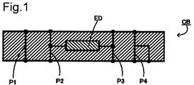
- FIG. 1 is a schematic cross sectional view illustrating the circuit board as the inspection object of the present invention.
- the circuit board as the inspection object of the present invention is a circuit board referred to a so-called embedded substrate, and is characterized in that an electronic component is built inside the circuit board.
- a circuit board CB illustrated in FIG. 1 four wiring patterns P (P1 to P4) and an electronic component ED are illustrated, and a wiring pattern P2 and a wiring pattern P3 are connected to the electronic component ED.
- the wiring pattern P2 is conductively connected to a GND terminal of the electronic component ED.
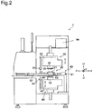
- FIG. 2 is a structural cross sectional view illustrating a circuit board inspection apparatus 1 in an embodiment of the present invention.
- FIG. 2 illustrates a rectangular coordinate system using XYZ axes, from the viewpoint of clarifying moving directions of a conveying table 20 and first and second inspection tool moving units 30 and 40.
- the Y axis has a positive direction which is directed from the front side to the back side of the paper of FIG. 1 .
- the circuit board inspection apparatus 1 is provided with a circuit board moving unit 60 for moving the conveying table 20 along the X axis, and the first and second inspection tool moving units 30 and 40 for moving, in a YZ surface, inspection tools 32 and 42 on which a plurality of probes (or contactors) 35 and 45 for circuit board inspection are mounted.
- the first and second inspection tool moving units 30 and 40 are arranged symmetrically with respect to a XY surface. The details of the inspection tools will be explained later, and the inspection tools will have reference numerals of 32 and 42 in the explanation of the configuration of the circuit board inspection apparatus 1.
- the conveying table 20 is provided with a circuit board holding unit 22 for mounting an inspection circuit board 21 thereon, and a cylinder bracket 63 fixed on a bottom surface of the inspection circuit board 21.
- the cylinder bracket 63 has a screw hole formed, wherein the screw hole pierces through the cylinder bracket 63 in a longitudinal direction.
- the circuit board moving unit 60 is provided with a ball screw 62 configured to engage with the screw hole of the bracket 63, and a drive unit 61 configured to rotate the ball screw 62.
- the screw thread and the thread groove on the ball screw 62 are not illustrated for simplification. If the ball screw 62 is rotated by the drive unit 61, the amount of movement and the moving directions along the X axis of the bracket 63, i.e. the conveying table 20, are determined depending on the amount and the direction of rotation of the ball screw 62.
- the first inspection tool moving unit 30 is provided with an inspection tool holding unit 33.
- the inspection tool holding unit 33 functions as holding the inspection tool 32 on which the plurality of probes 35 for circuit board inspection are mounted, and functions as moving the inspection tool 32 to make the plurality of probes 35 for circuit board inspection abut on inspection points of wires as the inspection objects on the inspection circuit board 21.
- the plurality of probes 35 for circuit board inspection and the like are electrically connected to a scanner (not illustrated) for inspecting and measuring the circuit board, via the inspection tool holding unit 33.
- the second inspection tool moving unit 40 is provided with an inspection tool holding unit 43, as in the inspection tool holding unit 33 of the first inspection tool moving unit 30.
- the inspection tool holding unit 43 functions as in the inspection tool holding unit 33.
- the movement of the first and second inspection tool moving units 30 and 40 and the circuit board moving unit 60 is controlled by a control apparatus (not illustrated) of the circuit board inspection apparatus 1.
- the first and second inspection tool moving units 30 and 40 have main cameras 34 and 44 installed, respectively, in order to specify the positions of the inspection circuit board 21 (or a sheet substrate B) and the conveying table 20.
- the circuit board inspection apparatus 1 has an inspecting device 70 for performing the electrical inspection of the circuit board CB.
- the inspecting device 70 has a configuration necessary for the electrical inspection of the circuit board CB.
- the inspecting device 70 has an electric power supply unit (not illustrated) configured to perform continuity or conduction inspection of a wiring pattern, a detection unit (not illustrated) configured to detect an electrical signal from the wiring pattern, a determination unit (not illustrated) configured to process and determine a detected signal from the detection unit, a change unit or a switching unit (not illustrated) configured to change a conduction pathway from a contactor, to each unit, and the like.
- the inspecting device 70 can be configured, for example, by adopting a direct current or alternating current power supply, an ammeter, a voltmeter, a switching element, and the like.
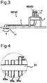
- FIG. 3 illustrates an embodiment of the circuit board inspection tool.
- the inspection tool 32 has the plurality of contactors 35 or 45, a holding body or a support body 3 configured to hold the contactors in a multi-needle manner, an electrode body 4 having electrode units configured to support the holding body 3 and configured to be in contact with the contactors 35 to be conductive to the circuit board inspection apparatus 1, a conducting wire unit 5 extended from and electrically connected to the electrode units, and a connection body 6 having connecting units 61 electrically connected to the circuit board inspection apparatus 1.
- FIG. 3 is a schematic side view for explaining the outline of the circuit board inspection tool 32.
- FIG. 3 illustrates three contactors 35, but the number of the contactors 35 is not particularly limited to this example.
- Each of the contactors 35 electrically connects the inspection point set in the wiring pattern P and respective one of the electrode units described later.
- the contactor 35 abuts on the inspection point at one end, and abuts on the electrode unit at the other end. Due to the contactor 35, the inspection point and the electrode unit are electrically connected.
- the contactor 35 is formed, for example, in an elongated rod shape, and can adopt a member having conductivity and flexibility. Moreover, the contactor 35 can also adopt a member using a spring which extends and contracts in the longitudinal direction.
- the electrode body 4 holds the electrode units (not illustrated) on which the contactors 35 abut at the other end and which are electrically connected to the circuit board inspection apparatus 1.
- the electrode units are formed to be substantially flush with the surface of the electrode body 4.
- Each of the electrode unit is preferably formed to be slightly greater than an outer diameter of respective one of the contactors 35.
- the conducting wire unit 5 electrically connects the electrode units of the electrode body 4 and the connecting units 61 of the connection body 6 described later.
- the conducting wire unit 5 is only required to electrically connect the electrode units 41 and the connecting units 61, and can adopt a linear metal wire such as, for example, a copper wire.
- the electrode body 4 is provided with through holes to place respective conducting wires in the through holes, and the conducting wires are cut to be flush with the surface of the electrode body 4.
- the electrode units can be formed.
- one ends of the metal wires function as the electrode units, and the other ends of the metal wires are conductively connected to the connecting units 61.
- connection body 6 holds the connecting units 61 electrically connected to the circuit board inspection apparatus 1.
- Each of the connecting units 61 is conductively connected to a connection point of the circuit board inspection apparatus 1, thereby being electrically connected to the circuit board inspection apparatus 1.
- the connection can adopt, for example, connector connection formed in an uneven shape (or in a concave and convex shape)
- the holding body 3 holds the contactors 35, guides one ends of the contactors 35 to the inspection points and guides the other ends of the contactors 35 to the electrode units.
- the holding body 3 in FIG. 3 is formed of two plate-like members disposed at a predetermined interval, and can bend the contactors 35 in a space formed by the two plate-like members.
- FIG. 4 is a partial enlarged view illustrating the circuit board inspection tool illustrated in FIG. 3 .
- the embodiment in FIG. 4 illustrates a state of the contactors 35 projecting from a plate-like member 31 on the upper side of the holding body 3.
- the circuit board inspection tool 3 in FIG. 4 has a contactor 35c which abuts on the inspection point on the wiring pattern conductively connected to the electronic component ED, a contactor 35a and a contactor 35c which abut on the inspection points on the wiring patterns not conductively connected to the electronic component ED.
- the amount of projection of the contactor 35c which abuts on the inspection point of the wiring pattern P conductively connected to the electronic component ED is formed to be greater than the amount of projection of the other contactors 35a and 35b (refer to FIG. 4 ).
- the contactor 35c firstly abuts on the inspection point of the circuit board CB. After that, the contactors 35a and 35b abut on the inspection points of the circuit board CB.
- the amount of projection of the contactor 35c which abuts on the wiring pattern P conductively connected to the electronic component ED is set to be longer than the amount of projection of the other contactors 35a and 35b, by a length A which is the sum of a size accuracy amount of the contactors 35 and a deflection amount of the circuit board. Due to the formation of the contactor 35c to be longer by the length A, in the case where the circuit board inspection tool 32 grips the circuit board CB, the contactor 35c can certainly abut on the circuit board CB before the other contactors 35 do, because the contactor 35c projects by the length A.
- the contactor 35c which abuts on the inspection point of the wiring pattern P conductively connected to the electronic component ED is disposed to be longer (or to project) by the length A; however, the contactor 35c set to be longer by the length A can be also set in the wiring pattern P which is connected to the GND terminal of the electrode component ED. Due to the setting of the contactor 35c in the wiring pattern P which is connected to the GND terminal of the electrode component ED, the damage of the electronic component ED can be prevented, more certainly.
- the circuit board CB as the inspection object is set.
- the contactor 35 which abuts on the inspection point set in the wiring pattern P conductively connected to the electronic component ED of the circuit board CB as the inspection object is specified.
- the specified contactor 35 is set such that the amount of projection from the plate-like member of the holding body 3 is longer by a predetermined length A than that of the contactors 35 which abut on the inspection points set in the wiring patterns P not conductively connected to the electronic component ED (or the other contactors 35).
- the upper-side circuit board inspection tool 32 and the lower-side circuit board inspection tool 42 are prepared depending on the inspection points of the circuit board CB.
- the inspection is started.
- the circuit board CB is gripped by the upper-side circuit board inspection tool 32 and the lower-side circuit board inspection tool 42.
- the contactor 35 or 45 which abuts on the wiring pattern P (or the wiring pattern P2 in FIG. 1 ) conductively connected to the electronic component ED is formed to be longer by the predetermined length A.
- the contactor which abuts on the wiring pattern P2 connected to the GND terminal of the electronic component ED is disposed to project by the length A.
- the circuit board inspection apparatus 1 moves each of the upper-side circuit board inspection tool 32 and the lower-side circuit board inspection tool 42 to abut on the surface of the circuit board CB. At this time, the circuit board inspection apparatus 1 performs switching to ground the contactor 35 or 45 connected to the wiring pattern P2 connected to the electronic component ED. Thus, the contactors abut on the circuit board CB in a grounded state.
- the contactor 35 or 45 conductively connected to the electronic component ED firstly abuts on the inspection point of the circuit board CB. At this time, even if there is stray capacitance in the circuit board CB itself, electricity is discharged from the circuit board inspection apparatus 1 via the circuit board inspection tool 32 or 42, and the damage of the electronic component ED of the circuit board ED can be thus prevented.
- the circuit board inspection apparatus 1 moves the upper-side circuit board inspection tool 32 and the lower-side circuit board inspection tool 42 until the circuit board CB can be gripped (or until all the contactors abut on the inspection points).
- circuit board inspection apparatus 1 sets each of the upper-side circuit board inspection tool 32 and the lower-side circuit board inspection tool 42 on the circuit board CB, the electrical inspection is performed on each of the wiring patterns P.
- circuit board inspection apparatus 1 moves the upper-side circuit board inspection tool 32 and the lower-side circuit board inspection tool 42 to be separated from the circuit board CB.
- the circuit board inspection apparatus 1 due to the movement of the circuit board inspection apparatus 1, it is possible to prevent the damage of the electronic component ED due to the occurrence of the excess current caused by the separation discharge which occurs in the case where the circuit board inspection tools are separated from the circuit board.
- the present invention it is possible to protect the electronic component ED from the discharge caused by that the circuit board inspection tools abutting on and being separated from the circuit board CB, and it is possible to prevent the damage of the electronic component ED by the inspection.
Landscapes
- Engineering & Computer Science (AREA)
- Physics & Mathematics (AREA)
- General Physics & Mathematics (AREA)
- Computer Hardware Design (AREA)
- Microelectronics & Electronic Packaging (AREA)
- General Engineering & Computer Science (AREA)
- Testing Of Short-Circuits, Discontinuities, Leakage, Or Incorrect Line Connections (AREA)
- Tests Of Electronic Circuits (AREA)
- Measuring Leads Or Probes (AREA)
Claims (6)
- Ein Leiterplattenprüfverfahren zum Prüfen von Verdrahtungsmustern (P1, P2, P3, P4) auf einer Leiterplatte (CB) mit einem eingebauten elektronischen Bauteil (ED) durch Verwenden einer Leiterplattenprüfvorrichtung (1), die ausgebildet ist, um eine elektrische Prüfung der auf der Leiterplatte (CB) gebildeten Verdrahtungsmuster (P1, P2, P3, P4) durchzuführen, und eines Leiterplattenprüfwerkzeuges (32, 42), welches eine Mehrzahl von Schützen (35a, 35b, 35c) zum elektrischen Verbinden der Leiterplatte (CB) und der Leiterplattenprüfvorrichtung aufweist, wobei das Leiterplattenprüfverfahren die Schritte aufweist:Erden eines Verdrahtungsmusters (P2), welches elektronisch mit dem elektronischen Bauteil der Leiterplatte (CB) verbunden ist, mittels eines Schützes (35c) der Mehrzahl von Schützen des Leiterplattenprüfwerkzeugs (32, 42), wobei ein Projektionsbetrag des Schützes (35c) größer gebildet ist als ein Projektionsbetrag der anderen Schütze (35a, 35b) der Mehrzahl von Schützen,In-leitfähigen-Kontakt-Bringen aller Verdrahtungsmuster (P1, P3, P4), außer dem geerdeten Verdrahtungsmuster (P2) der Verdrahtungsmuster (P1, P2, P3, P4), die auf der Leiterplatte (CB) gebildet sind, mit der Leiterplattenprüfvorrichtung (1) mittels der anderen Schütze (35a, 35b) des Leiterplattenprüfwerkzeugs (32, 42), undÜbertragen und Empfangen eines elektrischen Signals von der Leiterplattenprüfvorrichtung (1) zu und von der Leiterplatte (CB) mittels des Leiterplattenprüfwerkzeugs (1), und dadurch Durchführen der elektrischen Prüfung der Leiterplatte (CB).
- Das Leiterplattenprüfverfahren gemäß Anspruch 1, ferner aufweisend die Schritte:nach Durchführen der elektrischen Prüfung, Erden aller auf der Leiterplatte (CB) gebildeten Verdrahtungsmuster (P1, P2, P3, P4) durch die Leiterplattenprüfvorrichtung (1) mit Hilfe der Mehrzahl von Schützen (35a, 35b, 35c) des Leiterplattenprüfwerkzeugs (32, 42), undTrennen des Leiterplattenprüfwerkzeugs (1) von der Leiterplatte (CB) in einem Zustand, in dem die Mehrzahl von Schützen (35a, 35b, 35c) geerdet sind.
- Ein Leiterplattenprüfwerkzeug (32, 42), das ausgebildet ist, um eine Leiterplatte (CB) mit einem eingebauten elektronischen Bauteil (ED) und eine Leiterplattenprüfvorrichtung (1), die zum Prüfen einer Mehrzahl von auf der Leiterplatte (CB) gebildeten Verdrahtungsmustern (P1, P2, P3, P4) ausgebildet ist, elektrisch zu verbinden, wobei das Leiterplattenprüfwerkzeug (32, 42) aufweist:eine Mehrzahl von Schützen (35a, 35b, 35c), welche an einem Ende an Prüfpunkte auf den Verdrahtungsmustern anstoßen,einen Elektrodenkörper (4), welcher Elektrodeneinheiten hat, an die die jeweiligen Schütze (35a, 35b, 35c) an dem anderen Ende anstoßen und die elektrisch mit der Leiterplattenprüfvorrichtung (1) verbunden sind, undeinen Haltekörper (3), der eine Prüfseiten-Halteeinheit, welche ausgebildet ist, um eine Enden der Schütze (35a, 35b, 35c) zu den Prüfpunkten zu führen und eine Elektrodenseite-Halteeinheit aufweist, die ausgebildet ist, um die anderen Enden der Schütze zu den Elektrodeneinheiten zu führen, wobeiein Projektionsbetrag eines Schützes (35c), welcher in einem geerdeten Zustand an einen Prüfpunkt eines Verdrahtungsmusters (P2), das leitfähig mit dem elektronischen Bauteil (ED) verbunden ist, anstößt, größer gebildet ist als ein Projektionsbetrag der anderen Schütze (35a, 35b), sodass der Schütz (35c) an dem Prüfpunkt anstößt, bevor die anderen Schütze (35a, 35b) an den anderen Prüfpunkten anstoßen.
- Das Leiterplattenprüfwerkzeug gemäß Anspruch 3, wobei der Projektionsbetrag des Kontakts (35c) festgelegt ist, länger als der Projektionsbetrag der anderen Schütze (35b, 35c) zu sein, um eine Länge, die die Summe eines Maßhaltigkeitsbetrags der Schütze (35a, 35b, 35c) und eines Biegebetrages der Leiterplatte (CB) ist.
- Das Leiterplattenprüfwerkzeug gemäß Anspruch 3 oder 4, wobei das Verdrahtungsmuster (P2), das mit dem elektrischen Bauteil (ED) verbunden ist, mit einem Masse-Anschluss des elektrischen Bauteils (ED) verbunden ist.
- Eine Leiterplattenprüfvorrichtung (1), ausgebildet zum Prüfen einer Mehrzahl von Verdrahtungsmustern (P1, P2, P3, P4), die auf einer Leiterplatte (CB) mit einem eingebauten elektronischen Bauteil (ED) gebildet sind, wobei die Leiterplattenprüfvorrichtung (1) aufweist:ein Leiterplattenprüfwerkzeug (32, 42) gemäß Anspruch 3 oder 4, um ein Verdrahtungsmuster (P1, P2, P3, P4) der Leiterplatte (CB) als ein Prüfobjekt und die Leiterplattenprüfvorrichtung (1) leitfähig zu verbinden,einen Bewegungsmechanismus (30, 40) um das Leiterplattenprüfwerkzeug (32, 42) zu veranlassen, an die Leiterplatte (CB) anzustoßen,eine Prüfvorrichtung (70) zum Prüfen elektrischer Merkmale des Verdrahtungsmusters (P1, P2, P3, P4), undeine Steuervorrichtung zum Steuern des Bewegungsmechanismus (30, 40) und der Prüfvorrichtung (70), wobeidie Steuervorrichtung den Bewegungsmechanismus (30, 40) aktiviert, um das Leiterplattenprüfwerkzeug (32, 42) zu veranlassen an die Leiterplatte (CB) anzustoßen, und die Prüfvorrichtung (70) aktiviert, um den Schütz (35c) zu erden, der mit dem Verdrahtungsmuster (P2) in Kontakt ist, das elektronisch mit dem elektronischen Bauteil (ED) verbunden ist.
Applications Claiming Priority (1)
| Application Number | Priority Date | Filing Date | Title |
|---|---|---|---|
| JP2013117746A JP6221358B2 (ja) | 2013-06-04 | 2013-06-04 | 基板検査方法、及び基板検査装置 |
Publications (2)
| Publication Number | Publication Date |
|---|---|
| EP2811304A1 EP2811304A1 (de) | 2014-12-10 |
| EP2811304B1 true EP2811304B1 (de) | 2016-07-27 |
Family
ID=50842116
Family Applications (1)
| Application Number | Title | Priority Date | Filing Date |
|---|---|---|---|
| EP14170256.3A Not-in-force EP2811304B1 (de) | 2013-06-04 | 2014-05-28 | Leiterplattenprüfverfahren, Leiterplattenprüfvorrichtung und Leiterplattenprüfwerkzeug |
Country Status (5)
| Country | Link |
|---|---|
| US (1) | US20140354316A1 (de) |
| EP (1) | EP2811304B1 (de) |
| JP (1) | JP6221358B2 (de) |
| KR (1) | KR102232044B1 (de) |
| TW (1) | TWI635297B (de) |
Families Citing this family (8)
| Publication number | Priority date | Publication date | Assignee | Title |
|---|---|---|---|---|
| WO2016110198A1 (zh) * | 2015-01-07 | 2016-07-14 | 史拓莱姆有限公司 | 检测装置 |
| CN105301476B (zh) * | 2015-10-14 | 2018-06-22 | 京东方科技集团股份有限公司 | 用于印刷电路板的信号测试装置 |
| KR101656047B1 (ko) * | 2016-03-23 | 2016-09-09 | 주식회사 나노시스 | 기판 검사용 지그 |
| KR102015974B1 (ko) * | 2019-05-08 | 2019-08-28 | 엘엠디지털 주식회사 | 인쇄회로기판의 내전압 검사용 지그 |
| KR102245761B1 (ko) * | 2021-01-13 | 2021-04-28 | 엘엠디지털 주식회사 | 멀티 그리드 베이스가 구비된 인쇄회로기판 검사용 지그 |
| JP7719650B2 (ja) * | 2021-07-15 | 2025-08-06 | 日置電機株式会社 | 基板検査装置 |
| JP7784712B2 (ja) * | 2022-01-31 | 2025-12-12 | ヤマハファインテック株式会社 | 電気検査装置及び電気検査方法 |
| KR102451715B1 (ko) | 2022-07-05 | 2022-10-07 | (주)승진전자 | Atm용 pcb 기능검사장치 |
Family Cites Families (28)
| Publication number | Priority date | Publication date | Assignee | Title |
|---|---|---|---|---|
| JPS61117473A (ja) * | 1984-11-13 | 1986-06-04 | Ibiden Co Ltd | プリント配線板の検査方法とその検査装置 |
| JPH0690872B2 (ja) * | 1986-08-18 | 1994-11-14 | 東京電気株式会社 | メモリ−カ−ド装置 |
| US6229320B1 (en) * | 1994-11-18 | 2001-05-08 | Fujitsu Limited | IC socket, a test method using the same and an IC socket mounting mechanism |
| US5831441A (en) * | 1995-06-30 | 1998-11-03 | Fujitsu Limited | Test board for testing a semiconductor device, method of testing the semiconductor device, contact device, test method using the contact device, and test jig for testing the semiconductor device |
| US5705932A (en) * | 1995-10-10 | 1998-01-06 | Xilinx, Inc. | System for expanding space provided by test computer to test multiple integrated circuits simultaneously |
| JP3165056B2 (ja) * | 1997-02-28 | 2001-05-14 | 日本電産リード株式会社 | 基板検査装置および基板検査方法 |
| JP3104906B2 (ja) * | 1997-05-13 | 2000-10-30 | 日本電産リード株式会社 | 基板位置ずれ検出装置および基板位置ずれ検出方法 |
| JP3227697B2 (ja) * | 1998-01-16 | 2001-11-12 | ソニーケミカル株式会社 | 回路基板の検査方法及び装置 |
| JPH11242064A (ja) * | 1998-02-25 | 1999-09-07 | Fuji Photo Film Co Ltd | 実装基板検査装置 |
| EP0962777A3 (de) * | 1998-06-02 | 2002-12-11 | Nihon Densan Read Kabushiki Kaisha, (Nidec-Read Corporation) | Leiterplattentestvorrichtung |
| JP2002048845A (ja) * | 2000-08-02 | 2002-02-15 | Fuji Photo Film Co Ltd | 回路基板検査器 |
| JP2003344474A (ja) * | 2002-05-27 | 2003-12-03 | Oht Inc | 検査装置及び検査方法 |
| JP2006011507A (ja) | 2004-06-22 | 2006-01-12 | Nec Toppan Circuit Solutions Inc | 基板埋め込み部品のテストポイント設定方式 |
| JP3775509B2 (ja) * | 2004-07-15 | 2006-05-17 | Jsr株式会社 | 回路基板の検査装置および回路基板の検査方法 |
| JP2007183164A (ja) * | 2006-01-06 | 2007-07-19 | Fujitsu Ltd | 半導体集積回路装置及びその試験方法 |
| TW200729373A (en) * | 2006-01-20 | 2007-08-01 | Advanced Semiconductor Eng | Test module for wafer |
| JP4041831B2 (ja) * | 2006-05-15 | 2008-02-06 | 日本電産リード株式会社 | 基板検査用治具及びこの治具における接続電極部の電極構造 |
| JP2007315838A (ja) * | 2006-05-24 | 2007-12-06 | Epson Imaging Devices Corp | 検査装置及び検査方法 |
| US8624140B2 (en) * | 2006-07-10 | 2014-01-07 | Fujitsu Component Limited | Key switch and keyboard |
| US7400135B1 (en) * | 2007-02-23 | 2008-07-15 | Quality One Test Fixturing, Inc. | Test fixture and method for circuit board testing |
| JP5079592B2 (ja) | 2008-05-13 | 2012-11-21 | 日置電機株式会社 | データ生成装置およびデータ生成方法 |
| JP5374079B2 (ja) * | 2008-06-20 | 2013-12-25 | 東京エレクトロン株式会社 | 検査用接触構造体 |
| US8275223B2 (en) * | 2009-02-02 | 2012-09-25 | Ibiden Co., Ltd. | Opto-electrical hybrid wiring board and method for manufacturing the same |
| JP5365381B2 (ja) * | 2009-07-09 | 2013-12-11 | 大日本印刷株式会社 | 回路板の検査方法、回路板の検査装置 |
| TWI400450B (zh) * | 2009-09-30 | 2013-07-01 | Chunghwa Picture Tubes Ltd | 測試裝置 |
| JP5648809B2 (ja) * | 2011-10-28 | 2015-01-07 | 株式会社島津製作所 | Tftアレイ検査装置 |
| US20130200915A1 (en) * | 2012-02-06 | 2013-08-08 | Peter G. Panagas | Test System with Test Trays and Automated Test Tray Handling |
| US9285416B2 (en) * | 2012-04-02 | 2016-03-15 | Samsung Electronics Co., Ltd. | Apparatus and method for manufacturing substrates |
-
2013
- 2013-06-04 JP JP2013117746A patent/JP6221358B2/ja active Active
-
2014
- 2014-05-27 KR KR1020140063884A patent/KR102232044B1/ko active Active
- 2014-05-28 EP EP14170256.3A patent/EP2811304B1/de not_active Not-in-force
- 2014-06-03 US US14/294,187 patent/US20140354316A1/en not_active Abandoned
- 2014-06-03 TW TW103119295A patent/TWI635297B/zh active
Also Published As
| Publication number | Publication date |
|---|---|
| JP2014235112A (ja) | 2014-12-15 |
| TWI635297B (zh) | 2018-09-11 |
| JP6221358B2 (ja) | 2017-11-01 |
| TW201447334A (zh) | 2014-12-16 |
| US20140354316A1 (en) | 2014-12-04 |
| KR20140142661A (ko) | 2014-12-12 |
| KR102232044B1 (ko) | 2021-03-26 |
| EP2811304A1 (de) | 2014-12-10 |
Similar Documents
| Publication | Publication Date | Title |
|---|---|---|
| EP2811304B1 (de) | Leiterplattenprüfverfahren, Leiterplattenprüfvorrichtung und Leiterplattenprüfwerkzeug | |
| KR101101848B1 (ko) | 터치패널 검사장치 | |
| JPS6337261A (ja) | 同軸プロ−ブ | |
| KR20160092366A (ko) | 핀블록 및 이를 구비하는 검사 장치 | |
| KR20050085594A (ko) | 검사 방법 및 검사 장치 | |
| WO2014174852A1 (en) | Circuit board inspection apparatus and circuit board inspection method | |
| JP4773304B2 (ja) | 検査装置および検査方法 | |
| JP6219073B2 (ja) | 絶縁検査装置 | |
| KR101663920B1 (ko) | 기판 검사 방법 및 기판 검사용 지그 | |
| KR101359716B1 (ko) | 하네스 회로검사용 홀더 | |
| CN108469583A (zh) | 一种ict测试仪 | |
| KR101706465B1 (ko) | 프린트 기판 검사 장치 및 검사 방법 | |
| US9702906B2 (en) | Non-permanent termination structure for microprobe measurements | |
| KR101983732B1 (ko) | 검사용 치구 | |
| JP2014071091A (ja) | プローブユニットおよび検査装置 | |
| KR101287119B1 (ko) | 이어잭 어셈블리의 기능검사방법 및 장치 | |
| KR20140092242A (ko) | 검사 지그의 검사 방법 | |
| JP2014016300A (ja) | 基板検査装置および基板検査方法 | |
| JP3187208B2 (ja) | 回路基板検査機の部品有無検出プローブ | |
| JP2809304B2 (ja) | Ic試験装置の検査装置 | |
| CN117783609A (zh) | 一种pin针检测装置 | |
| JP5146109B2 (ja) | 検査装置 | |
| JP2006029950A (ja) | 同軸ケーブル及びそれを用いた測定装置 | |
| JP2009250659A (ja) | 治具試験装置及び治具試験方法 | |
| JP6046426B2 (ja) | 基板検査装置および基板検査方法 |
Legal Events
| Date | Code | Title | Description |
|---|---|---|---|
| PUAI | Public reference made under article 153(3) epc to a published international application that has entered the european phase |
Free format text: ORIGINAL CODE: 0009012 |
|
| 17P | Request for examination filed |
Effective date: 20140528 |
|
| AK | Designated contracting states |
Kind code of ref document: A1 Designated state(s): AL AT BE BG CH CY CZ DE DK EE ES FI FR GB GR HR HU IE IS IT LI LT LU LV MC MK MT NL NO PL PT RO RS SE SI SK SM TR |
|
| AX | Request for extension of the european patent |
Extension state: BA ME |
|
| RBV | Designated contracting states (corrected) |
Designated state(s): AL AT BE BG CH CY CZ DE DK EE ES FI FR GB GR HR HU IE IS IT LI LT LU LV MC MK MT NL NO PL PT RO RS SE SI SK SM TR |
|
| GRAP | Despatch of communication of intention to grant a patent |
Free format text: ORIGINAL CODE: EPIDOSNIGR1 |
|
| INTG | Intention to grant announced |
Effective date: 20160218 |
|
| GRAS | Grant fee paid |
Free format text: ORIGINAL CODE: EPIDOSNIGR3 |
|
| GRAA | (expected) grant |
Free format text: ORIGINAL CODE: 0009210 |
|
| AK | Designated contracting states |
Kind code of ref document: B1 Designated state(s): AL AT BE BG CH CY CZ DE DK EE ES FI FR GB GR HR HU IE IS IT LI LT LU LV MC MK MT NL NO PL PT RO RS SE SI SK SM TR |
|
| REG | Reference to a national code |
Ref country code: GB Ref legal event code: FG4D |
|
| REG | Reference to a national code |
Ref country code: CH Ref legal event code: EP |
|
| REG | Reference to a national code |
Ref country code: AT Ref legal event code: REF Ref document number: 816220 Country of ref document: AT Kind code of ref document: T Effective date: 20160815 |
|
| REG | Reference to a national code |
Ref country code: IE Ref legal event code: FG4D |
|
| REG | Reference to a national code |
Ref country code: DE Ref legal event code: R096 Ref document number: 602014002840 Country of ref document: DE |
|
| REG | Reference to a national code |
Ref country code: LT Ref legal event code: MG4D |
|
| REG | Reference to a national code |
Ref country code: NL Ref legal event code: MP Effective date: 20160727 |
|
| REG | Reference to a national code |
Ref country code: AT Ref legal event code: MK05 Ref document number: 816220 Country of ref document: AT Kind code of ref document: T Effective date: 20160727 |
|
| PG25 | Lapsed in a contracting state [announced via postgrant information from national office to epo] |
Ref country code: IS Free format text: LAPSE BECAUSE OF FAILURE TO SUBMIT A TRANSLATION OF THE DESCRIPTION OR TO PAY THE FEE WITHIN THE PRESCRIBED TIME-LIMIT Effective date: 20161127 Ref country code: FI Free format text: LAPSE BECAUSE OF FAILURE TO SUBMIT A TRANSLATION OF THE DESCRIPTION OR TO PAY THE FEE WITHIN THE PRESCRIBED TIME-LIMIT Effective date: 20160727 Ref country code: RS Free format text: LAPSE BECAUSE OF FAILURE TO SUBMIT A TRANSLATION OF THE DESCRIPTION OR TO PAY THE FEE WITHIN THE PRESCRIBED TIME-LIMIT Effective date: 20160727 Ref country code: NO Free format text: LAPSE BECAUSE OF FAILURE TO SUBMIT A TRANSLATION OF THE DESCRIPTION OR TO PAY THE FEE WITHIN THE PRESCRIBED TIME-LIMIT Effective date: 20161027 Ref country code: IT Free format text: LAPSE BECAUSE OF FAILURE TO SUBMIT A TRANSLATION OF THE DESCRIPTION OR TO PAY THE FEE WITHIN THE PRESCRIBED TIME-LIMIT Effective date: 20160727 Ref country code: HR Free format text: LAPSE BECAUSE OF FAILURE TO SUBMIT A TRANSLATION OF THE DESCRIPTION OR TO PAY THE FEE WITHIN THE PRESCRIBED TIME-LIMIT Effective date: 20160727 Ref country code: NL Free format text: LAPSE BECAUSE OF FAILURE TO SUBMIT A TRANSLATION OF THE DESCRIPTION OR TO PAY THE FEE WITHIN THE PRESCRIBED TIME-LIMIT Effective date: 20160727 Ref country code: LT Free format text: LAPSE BECAUSE OF FAILURE TO SUBMIT A TRANSLATION OF THE DESCRIPTION OR TO PAY THE FEE WITHIN THE PRESCRIBED TIME-LIMIT Effective date: 20160727 |
|
| PG25 | Lapsed in a contracting state [announced via postgrant information from national office to epo] |
Ref country code: LV Free format text: LAPSE BECAUSE OF FAILURE TO SUBMIT A TRANSLATION OF THE DESCRIPTION OR TO PAY THE FEE WITHIN THE PRESCRIBED TIME-LIMIT Effective date: 20160727 Ref country code: AT Free format text: LAPSE BECAUSE OF FAILURE TO SUBMIT A TRANSLATION OF THE DESCRIPTION OR TO PAY THE FEE WITHIN THE PRESCRIBED TIME-LIMIT Effective date: 20160727 Ref country code: ES Free format text: LAPSE BECAUSE OF FAILURE TO SUBMIT A TRANSLATION OF THE DESCRIPTION OR TO PAY THE FEE WITHIN THE PRESCRIBED TIME-LIMIT Effective date: 20160727 Ref country code: BE Free format text: LAPSE BECAUSE OF FAILURE TO SUBMIT A TRANSLATION OF THE DESCRIPTION OR TO PAY THE FEE WITHIN THE PRESCRIBED TIME-LIMIT Effective date: 20160727 Ref country code: PL Free format text: LAPSE BECAUSE OF FAILURE TO SUBMIT A TRANSLATION OF THE DESCRIPTION OR TO PAY THE FEE WITHIN THE PRESCRIBED TIME-LIMIT Effective date: 20160727 Ref country code: SE Free format text: LAPSE BECAUSE OF FAILURE TO SUBMIT A TRANSLATION OF THE DESCRIPTION OR TO PAY THE FEE WITHIN THE PRESCRIBED TIME-LIMIT Effective date: 20160727 Ref country code: GR Free format text: LAPSE BECAUSE OF FAILURE TO SUBMIT A TRANSLATION OF THE DESCRIPTION OR TO PAY THE FEE WITHIN THE PRESCRIBED TIME-LIMIT Effective date: 20161028 Ref country code: PT Free format text: LAPSE BECAUSE OF FAILURE TO SUBMIT A TRANSLATION OF THE DESCRIPTION OR TO PAY THE FEE WITHIN THE PRESCRIBED TIME-LIMIT Effective date: 20161128 |
|
| PG25 | Lapsed in a contracting state [announced via postgrant information from national office to epo] |
Ref country code: RO Free format text: LAPSE BECAUSE OF FAILURE TO SUBMIT A TRANSLATION OF THE DESCRIPTION OR TO PAY THE FEE WITHIN THE PRESCRIBED TIME-LIMIT Effective date: 20160727 Ref country code: EE Free format text: LAPSE BECAUSE OF FAILURE TO SUBMIT A TRANSLATION OF THE DESCRIPTION OR TO PAY THE FEE WITHIN THE PRESCRIBED TIME-LIMIT Effective date: 20160727 |
|
| REG | Reference to a national code |
Ref country code: DE Ref legal event code: R097 Ref document number: 602014002840 Country of ref document: DE |
|
| REG | Reference to a national code |
Ref country code: FR Ref legal event code: PLFP Year of fee payment: 4 |
|
| PG25 | Lapsed in a contracting state [announced via postgrant information from national office to epo] |
Ref country code: BG Free format text: LAPSE BECAUSE OF FAILURE TO SUBMIT A TRANSLATION OF THE DESCRIPTION OR TO PAY THE FEE WITHIN THE PRESCRIBED TIME-LIMIT Effective date: 20161027 Ref country code: SM Free format text: LAPSE BECAUSE OF FAILURE TO SUBMIT A TRANSLATION OF THE DESCRIPTION OR TO PAY THE FEE WITHIN THE PRESCRIBED TIME-LIMIT Effective date: 20160727 Ref country code: CZ Free format text: LAPSE BECAUSE OF FAILURE TO SUBMIT A TRANSLATION OF THE DESCRIPTION OR TO PAY THE FEE WITHIN THE PRESCRIBED TIME-LIMIT Effective date: 20160727 Ref country code: SK Free format text: LAPSE BECAUSE OF FAILURE TO SUBMIT A TRANSLATION OF THE DESCRIPTION OR TO PAY THE FEE WITHIN THE PRESCRIBED TIME-LIMIT Effective date: 20160727 Ref country code: DK Free format text: LAPSE BECAUSE OF FAILURE TO SUBMIT A TRANSLATION OF THE DESCRIPTION OR TO PAY THE FEE WITHIN THE PRESCRIBED TIME-LIMIT Effective date: 20160727 |
|
| PLBE | No opposition filed within time limit |
Free format text: ORIGINAL CODE: 0009261 |
|
| STAA | Information on the status of an ep patent application or granted ep patent |
Free format text: STATUS: NO OPPOSITION FILED WITHIN TIME LIMIT |
|
| 26N | No opposition filed |
Effective date: 20170502 |
|
| PG25 | Lapsed in a contracting state [announced via postgrant information from national office to epo] |
Ref country code: SI Free format text: LAPSE BECAUSE OF FAILURE TO SUBMIT A TRANSLATION OF THE DESCRIPTION OR TO PAY THE FEE WITHIN THE PRESCRIBED TIME-LIMIT Effective date: 20160727 Ref country code: LU Free format text: LAPSE BECAUSE OF NON-PAYMENT OF DUE FEES Effective date: 20170531 |
|
| REG | Reference to a national code |
Ref country code: CH Ref legal event code: PL |
|
| PG25 | Lapsed in a contracting state [announced via postgrant information from national office to epo] |
Ref country code: MC Free format text: LAPSE BECAUSE OF FAILURE TO SUBMIT A TRANSLATION OF THE DESCRIPTION OR TO PAY THE FEE WITHIN THE PRESCRIBED TIME-LIMIT Effective date: 20160727 |
|
| REG | Reference to a national code |
Ref country code: IE Ref legal event code: MM4A |
|
| PG25 | Lapsed in a contracting state [announced via postgrant information from national office to epo] |
Ref country code: CH Free format text: LAPSE BECAUSE OF NON-PAYMENT OF DUE FEES Effective date: 20170531 Ref country code: LI Free format text: LAPSE BECAUSE OF NON-PAYMENT OF DUE FEES Effective date: 20170531 |
|
| PG25 | Lapsed in a contracting state [announced via postgrant information from national office to epo] |
Ref country code: LU Free format text: LAPSE BECAUSE OF NON-PAYMENT OF DUE FEES Effective date: 20170528 |
|
| PG25 | Lapsed in a contracting state [announced via postgrant information from national office to epo] |
Ref country code: IE Free format text: LAPSE BECAUSE OF NON-PAYMENT OF DUE FEES Effective date: 20170528 |
|
| REG | Reference to a national code |
Ref country code: FR Ref legal event code: PLFP Year of fee payment: 5 |
|
| PG25 | Lapsed in a contracting state [announced via postgrant information from national office to epo] |
Ref country code: MT Free format text: LAPSE BECAUSE OF NON-PAYMENT OF DUE FEES Effective date: 20170528 |
|
| PG25 | Lapsed in a contracting state [announced via postgrant information from national office to epo] |
Ref country code: AL Free format text: LAPSE BECAUSE OF FAILURE TO SUBMIT A TRANSLATION OF THE DESCRIPTION OR TO PAY THE FEE WITHIN THE PRESCRIBED TIME-LIMIT Effective date: 20160727 |
|
| PG25 | Lapsed in a contracting state [announced via postgrant information from national office to epo] |
Ref country code: HU Free format text: LAPSE BECAUSE OF FAILURE TO SUBMIT A TRANSLATION OF THE DESCRIPTION OR TO PAY THE FEE WITHIN THE PRESCRIBED TIME-LIMIT; INVALID AB INITIO Effective date: 20140528 |
|
| PG25 | Lapsed in a contracting state [announced via postgrant information from national office to epo] |
Ref country code: CY Free format text: LAPSE BECAUSE OF FAILURE TO SUBMIT A TRANSLATION OF THE DESCRIPTION OR TO PAY THE FEE WITHIN THE PRESCRIBED TIME-LIMIT Effective date: 20160727 |
|
| PG25 | Lapsed in a contracting state [announced via postgrant information from national office to epo] |
Ref country code: MK Free format text: LAPSE BECAUSE OF FAILURE TO SUBMIT A TRANSLATION OF THE DESCRIPTION OR TO PAY THE FEE WITHIN THE PRESCRIBED TIME-LIMIT Effective date: 20160727 |
|
| PG25 | Lapsed in a contracting state [announced via postgrant information from national office to epo] |
Ref country code: TR Free format text: LAPSE BECAUSE OF FAILURE TO SUBMIT A TRANSLATION OF THE DESCRIPTION OR TO PAY THE FEE WITHIN THE PRESCRIBED TIME-LIMIT Effective date: 20160727 |
|
| PGFP | Annual fee paid to national office [announced via postgrant information from national office to epo] |
Ref country code: FR Payment date: 20230519 Year of fee payment: 10 Ref country code: DE Payment date: 20230519 Year of fee payment: 10 |
|
| PGFP | Annual fee paid to national office [announced via postgrant information from national office to epo] |
Ref country code: GB Payment date: 20230523 Year of fee payment: 10 |
|
| REG | Reference to a national code |
Ref country code: DE Ref legal event code: R119 Ref document number: 602014002840 Country of ref document: DE |
|
| GBPC | Gb: european patent ceased through non-payment of renewal fee |
Effective date: 20240528 |
|
| PG25 | Lapsed in a contracting state [announced via postgrant information from national office to epo] |
Ref country code: DE Free format text: LAPSE BECAUSE OF NON-PAYMENT OF DUE FEES Effective date: 20241203 |
|
| PG25 | Lapsed in a contracting state [announced via postgrant information from national office to epo] |
Ref country code: FR Free format text: LAPSE BECAUSE OF NON-PAYMENT OF DUE FEES Effective date: 20240531 |
|
| PG25 | Lapsed in a contracting state [announced via postgrant information from national office to epo] |
Ref country code: GB Free format text: LAPSE BECAUSE OF NON-PAYMENT OF DUE FEES Effective date: 20240528 |