EP2682794B1 - A tunable bragg grating, a tunable laser diode using same, and a corresponding method - Google Patents
A tunable bragg grating, a tunable laser diode using same, and a corresponding method Download PDFInfo
- Publication number
- EP2682794B1 EP2682794B1 EP12184980.6A EP12184980A EP2682794B1 EP 2682794 B1 EP2682794 B1 EP 2682794B1 EP 12184980 A EP12184980 A EP 12184980A EP 2682794 B1 EP2682794 B1 EP 2682794B1
- Authority
- EP
- European Patent Office
- Prior art keywords
- waveguide
- openings
- ridge
- layer
- arrays
- Prior art date
- Legal status (The legal status is an assumption and is not a legal conclusion. Google has not performed a legal analysis and makes no representation as to the accuracy of the status listed.)
- Active
Links
- 238000000034 method Methods 0.000 title claims description 9
- 239000010410 layer Substances 0.000 claims description 96
- 230000003287 optical effect Effects 0.000 claims description 75
- 239000000758 substrate Substances 0.000 claims description 48
- 238000003491 array Methods 0.000 claims description 32
- 238000005253 cladding Methods 0.000 claims description 30
- 239000012792 core layer Substances 0.000 claims description 20
- 125000006850 spacer group Chemical group 0.000 claims description 19
- 238000009826 distribution Methods 0.000 claims description 13
- 238000010438 heat treatment Methods 0.000 claims description 12
- 229910000530 Gallium indium arsenide Inorganic materials 0.000 claims description 11
- 239000010409 thin film Substances 0.000 claims description 8
- 238000005459 micromachining Methods 0.000 claims description 4
- 230000008878 coupling Effects 0.000 claims description 3
- 238000010168 coupling process Methods 0.000 claims description 3
- 238000005859 coupling reaction Methods 0.000 claims description 3
- 230000001902 propagating effect Effects 0.000 claims description 2
- 230000003595 spectral effect Effects 0.000 description 6
- 238000005530 etching Methods 0.000 description 5
- 238000004519 manufacturing process Methods 0.000 description 3
- 239000000463 material Substances 0.000 description 3
- 230000000737 periodic effect Effects 0.000 description 3
- XKRFYHLGVUSROY-UHFFFAOYSA-N Argon Chemical compound [Ar] XKRFYHLGVUSROY-UHFFFAOYSA-N 0.000 description 2
- IJGRMHOSHXDMSA-UHFFFAOYSA-N Atomic nitrogen Chemical compound N#N IJGRMHOSHXDMSA-UHFFFAOYSA-N 0.000 description 2
- 230000009467 reduction Effects 0.000 description 2
- 238000004088 simulation Methods 0.000 description 2
- 238000001228 spectrum Methods 0.000 description 2
- 239000006096 absorbing agent Substances 0.000 description 1
- 229910052786 argon Inorganic materials 0.000 description 1
- 230000015556 catabolic process Effects 0.000 description 1
- 230000008859 change Effects 0.000 description 1
- 238000006731 degradation reaction Methods 0.000 description 1
- 230000002939 deleterious effect Effects 0.000 description 1
- 230000001627 detrimental effect Effects 0.000 description 1
- 238000005516 engineering process Methods 0.000 description 1
- 238000001914 filtration Methods 0.000 description 1
- 230000004907 flux Effects 0.000 description 1
- 230000020169 heat generation Effects 0.000 description 1
- 239000011261 inert gas Substances 0.000 description 1
- 238000002347 injection Methods 0.000 description 1
- 239000007924 injection Substances 0.000 description 1
- 230000003993 interaction Effects 0.000 description 1
- 229910052757 nitrogen Inorganic materials 0.000 description 1
- 238000002840 optical waveguide grating Methods 0.000 description 1
- 230000010355 oscillation Effects 0.000 description 1
- 238000013021 overheating Methods 0.000 description 1
- 230000003094 perturbing effect Effects 0.000 description 1
- 230000008569 process Effects 0.000 description 1
- MZLGASXMSKOWSE-UHFFFAOYSA-N tantalum nitride Chemical compound [Ta]#N MZLGASXMSKOWSE-UHFFFAOYSA-N 0.000 description 1
- 230000002123 temporal effect Effects 0.000 description 1
- 229910052724 xenon Inorganic materials 0.000 description 1
- FHNFHKCVQCLJFQ-UHFFFAOYSA-N xenon atom Chemical compound [Xe] FHNFHKCVQCLJFQ-UHFFFAOYSA-N 0.000 description 1
Images


Classifications
-
- H—ELECTRICITY
- H01—ELECTRIC ELEMENTS
- H01S—DEVICES USING THE PROCESS OF LIGHT AMPLIFICATION BY STIMULATED EMISSION OF RADIATION [LASER] TO AMPLIFY OR GENERATE LIGHT; DEVICES USING STIMULATED EMISSION OF ELECTROMAGNETIC RADIATION IN WAVE RANGES OTHER THAN OPTICAL
- H01S5/00—Semiconductor lasers
- H01S5/06—Arrangements for controlling the laser output parameters, e.g. by operating on the active medium
- H01S5/062—Arrangements for controlling the laser output parameters, e.g. by operating on the active medium by varying the potential of the electrodes
- H01S5/0625—Arrangements for controlling the laser output parameters, e.g. by operating on the active medium by varying the potential of the electrodes in multi-section lasers
- H01S5/06255—Controlling the frequency of the radiation
- H01S5/06256—Controlling the frequency of the radiation with DBR-structure
-
- H—ELECTRICITY
- H01—ELECTRIC ELEMENTS
- H01S—DEVICES USING THE PROCESS OF LIGHT AMPLIFICATION BY STIMULATED EMISSION OF RADIATION [LASER] TO AMPLIFY OR GENERATE LIGHT; DEVICES USING STIMULATED EMISSION OF ELECTROMAGNETIC RADIATION IN WAVE RANGES OTHER THAN OPTICAL
- H01S5/00—Semiconductor lasers
- H01S5/02—Structural details or components not essential to laser action
- H01S5/024—Arrangements for thermal management
- H01S5/02461—Structure or details of the laser chip to manipulate the heat flow, e.g. passive layers in the chip with a low heat conductivity
-
- H—ELECTRICITY
- H01—ELECTRIC ELEMENTS
- H01S—DEVICES USING THE PROCESS OF LIGHT AMPLIFICATION BY STIMULATED EMISSION OF RADIATION [LASER] TO AMPLIFY OR GENERATE LIGHT; DEVICES USING STIMULATED EMISSION OF ELECTROMAGNETIC RADIATION IN WAVE RANGES OTHER THAN OPTICAL
- H01S5/00—Semiconductor lasers
- H01S5/06—Arrangements for controlling the laser output parameters, e.g. by operating on the active medium
- H01S5/0607—Arrangements for controlling the laser output parameters, e.g. by operating on the active medium by varying physical parameters other than the potential of the electrodes, e.g. by an electric or magnetic field, mechanical deformation, pressure, light, temperature
- H01S5/0612—Arrangements for controlling the laser output parameters, e.g. by operating on the active medium by varying physical parameters other than the potential of the electrodes, e.g. by an electric or magnetic field, mechanical deformation, pressure, light, temperature controlled by temperature
-
- G—PHYSICS
- G02—OPTICS
- G02B—OPTICAL ELEMENTS, SYSTEMS OR APPARATUS
- G02B6/00—Light guides; Structural details of arrangements comprising light guides and other optical elements, e.g. couplings
- G02B6/10—Light guides; Structural details of arrangements comprising light guides and other optical elements, e.g. couplings of the optical waveguide type
- G02B6/12—Light guides; Structural details of arrangements comprising light guides and other optical elements, e.g. couplings of the optical waveguide type of the integrated circuit kind
- G02B2006/12083—Constructional arrangements
- G02B2006/12097—Ridge, rib or the like
-
- G—PHYSICS
- G02—OPTICS
- G02B—OPTICAL ELEMENTS, SYSTEMS OR APPARATUS
- G02B6/00—Light guides; Structural details of arrangements comprising light guides and other optical elements, e.g. couplings
- G02B6/10—Light guides; Structural details of arrangements comprising light guides and other optical elements, e.g. couplings of the optical waveguide type
- G02B6/12—Light guides; Structural details of arrangements comprising light guides and other optical elements, e.g. couplings of the optical waveguide type of the integrated circuit kind
- G02B2006/12083—Constructional arrangements
- G02B2006/12107—Grating
-
- G—PHYSICS
- G02—OPTICS
- G02B—OPTICAL ELEMENTS, SYSTEMS OR APPARATUS
- G02B6/00—Light guides; Structural details of arrangements comprising light guides and other optical elements, e.g. couplings
- G02B6/10—Light guides; Structural details of arrangements comprising light guides and other optical elements, e.g. couplings of the optical waveguide type
- G02B6/12—Light guides; Structural details of arrangements comprising light guides and other optical elements, e.g. couplings of the optical waveguide type of the integrated circuit kind
- G02B2006/12166—Manufacturing methods
- G02B2006/12176—Etching
-
- H—ELECTRICITY
- H01—ELECTRIC ELEMENTS
- H01S—DEVICES USING THE PROCESS OF LIGHT AMPLIFICATION BY STIMULATED EMISSION OF RADIATION [LASER] TO AMPLIFY OR GENERATE LIGHT; DEVICES USING STIMULATED EMISSION OF ELECTROMAGNETIC RADIATION IN WAVE RANGES OTHER THAN OPTICAL
- H01S5/00—Semiconductor lasers
- H01S5/02—Structural details or components not essential to laser action
- H01S5/026—Monolithically integrated components, e.g. waveguides, monitoring photo-detectors, drivers
- H01S5/0261—Non-optical elements, e.g. laser driver components, heaters
-
- H—ELECTRICITY
- H01—ELECTRIC ELEMENTS
- H01S—DEVICES USING THE PROCESS OF LIGHT AMPLIFICATION BY STIMULATED EMISSION OF RADIATION [LASER] TO AMPLIFY OR GENERATE LIGHT; DEVICES USING STIMULATED EMISSION OF ELECTROMAGNETIC RADIATION IN WAVE RANGES OTHER THAN OPTICAL
- H01S5/00—Semiconductor lasers
- H01S5/10—Construction or shape of the optical resonator, e.g. extended or external cavity, coupled cavities, bent-guide, varying width, thickness or composition of the active region
- H01S5/12—Construction or shape of the optical resonator, e.g. extended or external cavity, coupled cavities, bent-guide, varying width, thickness or composition of the active region the resonator having a periodic structure, e.g. in distributed feedback [DFB] lasers
- H01S5/1206—Construction or shape of the optical resonator, e.g. extended or external cavity, coupled cavities, bent-guide, varying width, thickness or composition of the active region the resonator having a periodic structure, e.g. in distributed feedback [DFB] lasers having a non constant or multiplicity of periods
- H01S5/1209—Sampled grating
-
- H—ELECTRICITY
- H01—ELECTRIC ELEMENTS
- H01S—DEVICES USING THE PROCESS OF LIGHT AMPLIFICATION BY STIMULATED EMISSION OF RADIATION [LASER] TO AMPLIFY OR GENERATE LIGHT; DEVICES USING STIMULATED EMISSION OF ELECTROMAGNETIC RADIATION IN WAVE RANGES OTHER THAN OPTICAL
- H01S5/00—Semiconductor lasers
- H01S5/10—Construction or shape of the optical resonator, e.g. extended or external cavity, coupled cavities, bent-guide, varying width, thickness or composition of the active region
- H01S5/12—Construction or shape of the optical resonator, e.g. extended or external cavity, coupled cavities, bent-guide, varying width, thickness or composition of the active region the resonator having a periodic structure, e.g. in distributed feedback [DFB] lasers
- H01S5/1234—Actively induced grating, e.g. acoustically or electrically induced
-
- H—ELECTRICITY
- H01—ELECTRIC ELEMENTS
- H01S—DEVICES USING THE PROCESS OF LIGHT AMPLIFICATION BY STIMULATED EMISSION OF RADIATION [LASER] TO AMPLIFY OR GENERATE LIGHT; DEVICES USING STIMULATED EMISSION OF ELECTROMAGNETIC RADIATION IN WAVE RANGES OTHER THAN OPTICAL
- H01S5/00—Semiconductor lasers
- H01S5/10—Construction or shape of the optical resonator, e.g. extended or external cavity, coupled cavities, bent-guide, varying width, thickness or composition of the active region
- H01S5/12—Construction or shape of the optical resonator, e.g. extended or external cavity, coupled cavities, bent-guide, varying width, thickness or composition of the active region the resonator having a periodic structure, e.g. in distributed feedback [DFB] lasers
- H01S5/1237—Lateral grating, i.e. grating only adjacent ridge or mesa
-
- H—ELECTRICITY
- H01—ELECTRIC ELEMENTS
- H01S—DEVICES USING THE PROCESS OF LIGHT AMPLIFICATION BY STIMULATED EMISSION OF RADIATION [LASER] TO AMPLIFY OR GENERATE LIGHT; DEVICES USING STIMULATED EMISSION OF ELECTROMAGNETIC RADIATION IN WAVE RANGES OTHER THAN OPTICAL
- H01S5/00—Semiconductor lasers
- H01S5/20—Structure or shape of the semiconductor body to guide the optical wave ; Confining structures perpendicular to the optical axis, e.g. index or gain guiding, stripe geometry, broad area lasers, gain tailoring, transverse or lateral reflectors, special cladding structures, MQW barrier reflection layers
- H01S5/22—Structure or shape of the semiconductor body to guide the optical wave ; Confining structures perpendicular to the optical axis, e.g. index or gain guiding, stripe geometry, broad area lasers, gain tailoring, transverse or lateral reflectors, special cladding structures, MQW barrier reflection layers having a ridge or stripe structure
Definitions
- the present invention relates to optical waveguides and lasers, and in particular to structures and methods for tuning optical waveguide gratings in lasers.
- a laser diode includes a p-n junction between a pair of mirrors for creating optical feedback for light generated and amplified at the p-n junction when a forward current is applied to the p-n junction.
- the mirrors are made wavelength selective, and a reflection wavelength of at least one of the mirrors is tuned.
- waveguide gratings are frequently used as wavelength selective mirrors.
- periodic perturbations of the effective refractive index of the waveguide are created to selectively reflect light at a wavelength corresponding to the spatial frequency of the periodic refractive index perturbations.
- a waveguide grating can be tuned by heating or, for waveguide gratings formed at a p-n junction, by providing a direct current to the p-n junction, which changes its overall refractive index through carrier injection.
- Suspended or thermally decoupled waveguides are also known from EP1841023 , US20090074020 , and US20090041073 .
- Placing grating tuning electrodes aligned with grating arrays is also known in the field (see EP1087612 , EP1804349 EP1753104 , US4885753 , GB2371920 , EP1478064 , GB2378311 , DE19629916 ).
- waveguides suspended over a substrate without additional structural support are prone to a mechanical failure. Multiple legs were used in a Cunningham device to support the suspended waveguide along their length, but these can result in an overly complex waveguide structure and/or interfere with the optical function of the waveguide.
- a waveguide Bragg grating is suspended over a substrate by plurality of fingers extending laterally away from the waveguide centerline, resulting in a simple and easily manufacturable structure.
- the Bragg grating 2. is in the form of a sampled grating, which consists of periodically spaced uniform grating bursts separated by blanked regions without gratings, and is characterized by a grating period of a high spatial frequency and a burst period of a low spatial frequency. More generally, the Bragg grating consist of a slow spatial modulation of the grating strength or the grating phase along the waveguide centerline or optical axis, forming crests and valleys of modulation. The crests and valleys can be of a square shape, such as in a sampled grating, or of a smooth, wave-like varying shape.
- the positions of the fingers are coordinated with the positions of the crests and valleys of modulation, to avoid disturbing the Bragg grating upon thermal tuning of the grating.
- the heat flows through the fingers, creating a quasi-periodic refractive index variation along the Bragg grating optical axis due to a quasi-periodic temperature variation created by the heat flow from the grating through the supporting fingers. Since the positions of the supporting fingers are coordinated with the positions of the grating modulation crests and valleys, the optical phase coherence is maintained between the grating modulation crests, so that the Bragg grating is not disturbed by the heating. As a result, smooth and continuous tuning of the Bragg grating is possible substantially without perturbing the reflection bandshape.
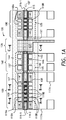
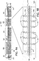
- a SG-DBR laser 120 of the invention includes front and back tunable Bragg gratings (DBR) 100, a gain section 126, and an optional phase section 160.
- DBR Bragg gratings
- the Bragg gratings 100, the gain section 126, and the phase section 160 are sections of a ridge waveguide structure having a common top ridge 115 for guiding a light mode 108.
- the Bragg gratings 100 include a first substrate section 102, first and second spaced apart support bars 104 extending upwardly from the first substrate section 102, a first ridge waveguide 106, and a first resistive heater 117.
- the first ridge waveguide 106 is supported by the first and second support bars 104 above the first substrate section 102, forming a first gap 105 between the first substrate section 102 and the first ridge waveguide 106.
- the first ridge waveguide 106 includes a stack of: a bottom cladding layer 110 supported by the first and second support bars 104, a core layer 112 disposed on the bottom cladding layer 110, and a top cladding layer 114 disposed on the core layer 112.
- the top cladding layer 114 has the ridge 115 on top, for guiding the light mode 108 along the ridge 115.
- the refractive index of the core layer 112 is higher than refractive indices of the top 114 and bottom 110 cladding layers, for confining the light 108 guided by the ridge 115 substantially to the core layer 112.
- the effective refractive index of the first ridge waveguide 106 is spatially modulated, forming a grating for reflecting an optical frequency component 109 of the light 108 guided by the first ridge waveguide 106 to propagate back therein.
- the refractive index of the core layer 112 can be spatially modulated, or the ridge 115 can be laterally corrugated to create the spatial modulation of the effective refractive index.
- At least one of phase or amplitude of the spatial modulation of the effective refractive index is varying along the optical axis, forming modulation crests 116-1 and valleys 116-2.
- the grating period can be about 0.24 micrometers
- the length of a sampled grating burst (modulation crest 116-1) can be 3 micrometers
- the burst period, or distance between neighboring crests 116-1 can be 50 micrometers.
- the first resistive heater 117 is disposed on an insulating dielectric layer, not shown, which is deposited on the top cladding layer 114.
- the first ridge waveguide 106 has first and second arrays of openings 118A and 118B, respectively, extending through the first ridge waveguide 106 and into the first gap 105.
- the openings 118A and 118B run on opposite sides of the ridge 115, defining first and second arrays of heat conducting fingers 119A and 119B, respectively, extending from the ridge 115 towards the first and second support bars 104.
- First and last openings 118C of the first array of the openings 118A are longer than the remainder of the openings 118A.
- the first and last openings 118D of the first array of the openings 118B are preferably longer than the remainder of the openings 118B.
- the longer openings 118C and 118D facilitate creation of a more uniform temperature distribution upon heating the DBR 100 by the first resistive heater 117. Both length and width of first and last openings 118C and 118D can be adjusted to improve the temperature uniformity.
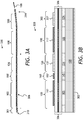
- the first ridge waveguide 106 can be burst-modulated ( FIG. 1B ) or smoothly modulated ( FIG. 1C ), or modulated in a more complicated manner.
- the modulation can include amplitude or phase modulation or both.
- the modulation can be periodic or quasi-periodic.
- the modulation crests 116-1 comprise bursts of a sampled Bragg grating, having substantially no modulation in the valleys 116-2 between the bursts 116-1.
- the modulation is more smooth, so that the modulation valleys 116-2 have some refractive index modulation.
- the modulation crests 116-1 are spaced apart at a first spatial frequency f 1 along an optical axis 107 of the first ridge waveguide 106. As shown in FIGs. 1B and 1C with dashed lines 150, positions of the heat conducting fingers 119A along the optical axis 107 are coordinated with positions of the modulation crests 116-1 and valleys 116-2 along the optical axis 107.
- the second spatial frequency f 2 of the heat conducting fingers 119A and 119B along the ridge 115 is an integer multiple of the first spatial frequency f 1 .
- f 2 2 f 1 ; and in FIG. 1C , the frequencies f 1 and f 2 are equal.
- the gain section 126 includes a substrate 122, which is preferably a common substrate with the first substrate section 102, a spacer layer 124 supported by the substrate 122, an active waveguide 126 for amplifying the light mode 108, and a first electrode 137 for providing electrical current to the active waveguide 126.
- the spacer layer 124 includes the first and second support bars 104 of the tunable DBR section, or Bragg grating 100.
- the active waveguide 126 is optically coupled to the tunable DBR section 100 and disposed in mechanical, thermal, and electrical contact with the spacer layer 124.
- the active waveguide layer 126 includes the stack of: a first conductivity type layer 130 supported by the spacer layer 124 and integrally formed with the bottom cladding layer 110; a junction layer 132 supported by the first conductivity type layer 130 and integrally formed with the core layer 112; and a second conductivity type layer 134 supported by the junction layer 132 and integrally formed with the top cladding layer.
- the ridge 115 runs through the first ridge waveguide 106 and the active waveguide 126 for providing optical coupling therebetween.
- the first and second conductivity type layers 130 and 134 include n- and p-doped InP layers, respectively, the junction layer 132 includes InGaAsP quantum wells, and the spacer layer 124 includes an InGaAs layer.
- the phase section 160 is a variant of the structure of the DBR section 100, lacking the spatial modulation of the refractive index.
- the phase section 160 includes a second substrate section 142, third and fourth support bars 144 extending upwardly from the second substrate section 142, and a second ridge waveguide 146 for guiding the light mode 108, supported by the third and fourth_support bars 144 above the second substrate section 142, forming a second gap 145 between the second substrate section 142 and the second ridge waveguide 146.
- the second ridge waveguide 146 includes the same stack as the first ridge waveguide 106, with the difference that the effective refractive index of the second ridge waveguide 146 is not spatially modulated.
- a second resistive heater 157 is disposed on the top cladding layer 114, for providing heating of the second ridge waveguide 146 for tuning optical phase of the light mode 108 propagating therein.
- the guided light mode 108 generated in the gain section 126 propagates along the ridge 115.
- An optical frequency component 109 of the guided light mode 108 is reflected to propagate back along the ridge 115 towards the gain section 126, thus providing an optical feedback to the laser 120.
- the reflected optical frequency component 109 has a wavelength corresponding to the spatial frequency of the effective refractive index modulation of the first ridge waveguide 106.
- the first resistive heater 117 provides heating to the first ridge waveguide 106, for tuning the optical frequency of the reflected optical frequency component 109.
- the heating by the first resistive heater 117 substantially does not disturb or modify the reflected frequency spectrum beyond simply tuning of the center frequency of the reflected frequency spectrum. This allows one to reduce a bandwidth variation as the laser 120 is tuned in optical frequency or wavelength.
- the first and second gaps 105 and 145 can be filled with a chemically inert gas such as xenon, argon, or nitrogen. Also, the first and second gaps 105 and 145 can form a single gap, although the latter structure will have somewhat increased thermal crosstalk between the tunable DBR and phase sections 100 and 160, respectively; this is why two separate gaps 105 and 145 are preferred.
- the gap 105 can be formed by lateral selective undercut etching of the sacrificial spacer layer 124.
- the gap 145 can be formed by selective etching of the spacer layer through the openings 118A , 118B, 118C, and 118D. These etching techniques are generally referred to as "micromachining", a term adopted from micro-electro-mechanical systems (MEMS) manufacturing.
- MEMS micro-electro-mechanical systems
- the first and second ridge waveguides 106 and 146, respectively, and the active waveguide 126 preferably form a single monolithic shallow-ridge waveguide structure having the active section 126, the tunable Bragg grating or DBR section 100, and the phase section 160.
- the openings 118A-118D and the gap 105 are particularly easy to form in shallow-ridge waveguides, ensuring ease of overall manufacture.
- the ridge type waveguides are only example embodiments of waveguides of the invention.
- Other waveguide types known to a person skilled in the art, can also be used in the tunable Bragg grating 100, the gain section 126, and/or the phase section 160.
- the other waveguide types must be suspended over the substrate 102 by the support bars 104, and the at least one of phase or amplitude of the spatial modulation of the effective refractive index of the Bragg grating 100 has to have a plurality of crests 116-1 and valleys 116-2.
- the positions of the heat conducting fingers 119A and 119B along the optical axis 107 have to be coordinated with the positions of the crests 116-1 and valleys 116-2 along the optical axis 107, to lessen the bandshape variation of the reflected optical frequency component 109.
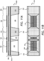
- an embodiment 320 of the SG-DBR laser 120 of FIG. 1A includes two tunable DBR sections 100, the phase section 160, the gain section 126, and an amplifier section 300 formed within a common shallow-ridge waveguide 306 suspended over the common substrate 122 at the tunable DBR sections 100 and the phase section 160.
- a back-facet absorber section 301 is provided for absorbing laser light at the left-hand side of the waveguide 306 in FIG. 3A , to prevent light reflected from a left facet 310 of the shallow-ridge waveguide 306 to interfere with light selectively reflected by the left tunable Bragg grating 100.
- a common backplane electrode 302 is electrically coupled to a back side of the substrate 122.
- the gain section 126 is powered with the first electrode 137, and the amplifier section 300 is powered by a second electrode 337 or providing electrical current to the amplifier section 300.
- the first and second electrodes 137 and 337, and the heaters 117 and 157 are omitted in FIG. 3A , so as not to hide the underlying structures.
- the function of the amplifier section 300 is to amplify the light 108 generated in the gain section 126, to provide a constant output power as the emission wavelength of the laser 320 is tuned by the synchronously tuned Bragg gratings 100.
- the output power can be measured by an integrated photodetector 314.
- the resistive heaters 117 of the tunable Bragg gratings 100 are uniform thin-film resistive heaters applied to the ridge 115 of the ridge waveguide 106, with current passing along the length of the heater 117 between two contact pads 117A.
- a passivating layer of dielectric is disposed between the thin-film heater 117 and the underlying ridge waveguide 106. Referring to FIGs. 4 , 5A, and 5B , with further reference to FIGs. 1A , 2A to 2C , 3A, and 3B , a numerical simulation has been performed for an embodiment 400 of the tunable Bragg grating 100 having the uniform heater 117 (not shown in FIG. 4 ) running along the ridge 115.
- Positions, lengths, and widths of the openings 118A to 118D are selected so as to create a substantially uniform temperature distribution along the ridge 115.
- the positions, lengths, and widths of the openings 118A to 118D define lengths and widths of the heat conducting fingers 119A and 119B.
- the openings 118A and 118B define a mesa 410 therebetween, and this mesa 410 limits the optical interaction between the optical mode 108 of the ridge waveguide 106 and the refractive index discontinuity resulting from the openings 118A, 118B.
- the length and width of the mesa 410 including end mesa sections 411 have an impact on the resulting temperature distribution. In the simulation of FIGs.
- the ridge 115 is 2 micrometers tall and 2 micrometers wide.
- the mesa width (distance between the openings 118A and 118B of the first and second arrays, respectively) is 20 micrometers
- the thickness of the mesa sections 410, 411 is 2 micrometers
- the height of the gap 105 (vertical dimension of the gap 105 in FIGs. 2A and 2B ) is 2 micrometers.
- the total length of the mesa 410 is 400 micrometers.
- the material is InP.
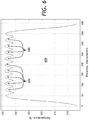
- FIG. 6 a longitudinal distribution 600 of the temperature of the waveguide sections 410, 411 is shown.
- the temperature varies from approximately 303°K to 334°K.
- the temperature along the mesa sections 410, 411 oscillates at approximately 3°K peak-to-peak amplitude, the peaks of the temperature distribution being denoted at 602.
- the peak temperatures have been made substantially uniform by optimizing the geometry of the end openings 118C and 118D and the end mesa sections 411, such that heat generation along the end mesa section 411 is balanced by heat conduction through the end mesa section 411 to the spacer layer 124 and the substrate 122. Since the positions of the heat conducting fingers 119A and 119B along the ridge 115 are coordinated with the positions of the modulation crests 116-1 along the ridge 115, the temperature oscillation peaks 602 are also coordinated with the positions of the modulation crests 116-1 (not shown in FIGs. 4 , 5A, 5B ), thus maintaining optical phase coherence of the optical signal 108 between the modulation crests 116-1.
- the spectral filtering properties of the Bragg grating 100 are very similar to those with an ideally even temperature profile. It is to be understood that the end mesa sections 411, where the temperature is varying from approximately the temperature of the substrate 102 at the ends to the peak temperature at the first fingers 119A and 119B, can minimally include gratings because of the highly non-uniform temperature profile.
- a simulated time trace 700 of temperature rise upon a quasi-instantaneous application of the 25mW of heater power shows that the 27.5°K temperature increase is achieved in less than 100 microseconds.
- the cooling-down time is also below 100 microseconds, which is more than 16 times faster than the tuning time reported by Ishii et al. in the above-mentioned paper entitled “Narrow spectral linewidth under wavelength tuning in thermally tunable super-structure grating (SSG) DBR lasers", published in IEEE Journal of Selected Topics in Quantum Electronics, Vol. 1, No. 2 (1995), pp. 401-407 .
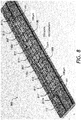
- a tunable Bragg grating 800 is a variant of the tunable Bragg grating 100 of FIG. 1A .
- the first resistive heater 117 includes a plurality of electrically coupled individual thin-film heaters 817 running on top of the heat conducting fingers 119A and 119B. Additional heater elements 817A are disposed on the ends 411 of the mesa 410, to further improve uniformity of the temperature distribution.
- a SG-DBR laser 820 is a variant of the SG-DBR laser 320 of FIG. 3A . In the SG-DBR laser 920 of FIG.
- the tunable Bragg gratings 100 of FIGs. 1A , 2A, and 2B have been replaced with the tunable Bragg gratings 800 of FIG. 8 .
- a comparable longitudinal heater for example a tantalum nitride (TaN) thin film of a same thickness, would have many times higher resistance. This connection of the individual heaters 817 can better match the impedance of driving electronics, not shown.
- the individual thin-film heaters 117 must run on top of at least some of the heat conducting fingers 119A and 119B. By placing heating elements 117 only on the heat conducting fingers 119A and 119B and on the ends 411 of the mesa 410, a substantial reduction in the longitudinal peak-to-peak temperature variation along the mesa 410 can be achieved.
- the spacer layer 124 can include a sacrificial InGaAs layer. 1-2 micrometer thick sacrificial InGaAs layer 124 provides a good electrical contact of the active waveguide 126 to the substrate 122. Detrimentally, such a thick sacrificial InGaAs layer 124 can be difficult to grow and subsequently micromachine to manufacture the support bars 104, and its thermal impedance will have a deleterious effect on active section performance.
- the spacer layer 124 can be made in form of a stack including several different layers. Referring to FIG. 1
- the spacer layer 124 includes in sequence from bottom to top a 20nm thick InGaAsP bottom etch stop layer 1002 having a bandgap wavelength of 1.2 ⁇ m, a 200nm thick InP bottom second stage sacrificial layer 1004, a 200nm thick first stage InGaAs sacrificial layer 1006, a 2000nm thick InP top second stage sacrificial layer 1008, and a 20nm thick InGaAsP top etch stop layer 1010.
- InP can be grown much more easily to a larger thickness than InGaAs.
- the thickness of the multilayer stack spacer layer 124 can be increased, the thickness of at least one of the InP sacrificial layers 1004 and 1008 being larger than the thickness of the InGaAs sacrificial layer 1006, and the total thickness of the InGaAs or InGaAsP material can be reduced.
- the spacer layer 124 of FIG. 10B can then be etched, or micromachined, in two etching steps, one for the InGaAs layer 1006 to achieve lateral undercut, and one for the InP layers 1004 and 1008 to etch vertically to achieve the thicker gap 105.
- a SG-DBR laser 1120 is an embodiment of the SG-DBR laser 320 of FIG. 3 .
- the first and second gaps 105 and 145 of the tunable Bragg grating sections 100 and the phase section 160, respectively extend completely through the substrate 122. This can be achieved by using bulk micromachining techniques known from MEMS technologies, by etching through the bottom of the substrate 122.
- any laser diode having an active waveguide for laser light generation for example the active waveguide 126 of FIG. 1A , can be tuned according to the invention by following the three steps A, B, and C.
- Step A includes providing a tunable Bragg grating such as the tunable DBR 100, having the first substrate section 102, the first and second spaced apart support bars 104 extending upwardly from the substrate section 102, and a first waveguide, for example the ridge waveguide 106 optically coupled to the active waveguide 126.
- the first waveguide 106 is supported by the support bars 104 above the first substrate section 102, forming the gap 105 between the first substrate section 102 and the first waveguide 106.
- the effective refractive index of the first waveguide is spatially modulated along the optical axis 107, forming a grating for reflecting the optical frequency component 109 of the light 108 guided by the ridge waveguide 106 to propagate back.
- At least one of phase or amplitude of the spatial modulation of the effective refractive index is varying along the optical axis, forming the modulation crests 116-1 and valleys 116-2 (best seen in FIGs. 1B and 1C ) spaced apart at a first spatial frequency f 1 along the optical axis 107.
- Step B includes providing first and second arrays of the openings 118A to 118D extending through the first waveguide 106 and into the gap 105, the openings 118A to 118D running on respective opposite first and second sides of the optical axis 107 as shown.
- the openings (118A, 118C) and (118B, 118D) define first and second arrays of heat conducting fingers 119A and 119B, respectively, extending from the optical axis 107 towards the support bars 104.
- Step B includes disposing the openings 118A to 118D so that positions of the heat conducting fingers 119A and 119B along the optical axis 107 are coordinated with the positions of the modulation crests 116-1 along the optical axis 107.
- Step B can also include disposing the first and last, or end openings 118C and 118D to achieve a substantially uniform longitudinal temperature profile along the length of the first waveguide 106 containing the grating.
- Step C includes heating the first waveguide 106 for tuning the optical frequency of the optical frequency component, thereby tuning the laser diode. Due to coordination of the position of the heat conducting fingers 119A and 119B with the modulation crests 116-1, the optical phase coherence of the light mode 108 is maintained between the modulation crests 116-1, so that the spectral bandshape of the light 109 reflected by the tunable Bragg grating 100 is not disturbed, or at least disturbed less, in the process of tuning.
- Step B comprises disposing the openings 118A to 118D so that the first and second arrays of the respective heat conducting fingers 119A and 119B are disposed at a second spatial frequency along the optical axis 107, wherein the second spatial frequency is an integer multiple of the first spatial frequency.
Landscapes
- Physics & Mathematics (AREA)
- Condensed Matter Physics & Semiconductors (AREA)
- General Physics & Mathematics (AREA)
- Electromagnetism (AREA)
- Optics & Photonics (AREA)
- Semiconductor Lasers (AREA)
- Optical Modulation, Optical Deflection, Nonlinear Optics, Optical Demodulation, Optical Logic Elements (AREA)
Applications Claiming Priority (1)
| Application Number | Priority Date | Filing Date | Title |
|---|---|---|---|
| US13/542,547 US8861556B2 (en) | 2012-07-05 | 2012-07-05 | Tunable Bragg grating and a tunable laser diode using same |
Publications (2)
| Publication Number | Publication Date |
|---|---|
| EP2682794A1 EP2682794A1 (en) | 2014-01-08 |
| EP2682794B1 true EP2682794B1 (en) | 2018-05-16 |
Family
ID=47048966
Family Applications (1)
| Application Number | Title | Priority Date | Filing Date |
|---|---|---|---|
| EP12184980.6A Active EP2682794B1 (en) | 2012-07-05 | 2012-09-19 | A tunable bragg grating, a tunable laser diode using same, and a corresponding method |
Country Status (4)
| Country | Link |
|---|---|
| US (1) | US8861556B2 (enExample) |
| EP (1) | EP2682794B1 (enExample) |
| JP (1) | JP6093660B2 (enExample) |
| CN (1) | CN103532009B (enExample) |
Families Citing this family (32)
| Publication number | Priority date | Publication date | Assignee | Title |
|---|---|---|---|---|
| EP2989699B1 (en) * | 2013-04-30 | 2019-12-25 | Huawei Technologies Co., Ltd. | Tunable laser with high thermal wavelength tuning efficiency |
| KR101672586B1 (ko) * | 2014-06-09 | 2016-11-04 | 한국과학기술원 | 파장 조율이 가능한 구조를 갖는 광 격자 커플러 |
| US9509119B2 (en) | 2015-01-13 | 2016-11-29 | Futurewei Technologies, Inc. | Tunable laser with a cascaded filter and comb reflector |
| CN105759350A (zh) * | 2015-07-03 | 2016-07-13 | 苏州峰通光电有限公司 | 一种有机无机混合集成热光调制型光栅及其制备方法 |
| EP3400635B1 (en) | 2016-01-04 | 2023-06-07 | Infinera Corporation | Tunable waveguide devices |
| CN105527730A (zh) * | 2016-01-06 | 2016-04-27 | 北京大学 | 一种光学相位调制器 |
| CN107230930A (zh) * | 2016-03-23 | 2017-10-03 | 华为技术有限公司 | 一种可调激光器及制备方法 |
| GB2554460A (en) * | 2016-09-29 | 2018-04-04 | Oclaro Tech Ltd | Waveguide structure |
| WO2018186471A1 (ja) * | 2017-04-06 | 2018-10-11 | 国立大学法人横浜国立大学 | 光偏向デバイス |
| CN108732667B (zh) * | 2017-04-17 | 2021-01-05 | 华为技术有限公司 | 一种超结构光栅和可调谐激光器 |
| CN108879309B (zh) * | 2017-05-09 | 2021-02-12 | 华为技术有限公司 | 用于可调激光器的反射镜结构和可调激光器 |
| CN108879310B (zh) * | 2017-05-10 | 2020-07-28 | 华为技术有限公司 | 用于可调激光器的反射镜结构和可调激光器 |
| WO2019116657A1 (ja) * | 2017-12-15 | 2019-06-20 | 株式会社堀場製作所 | 半導体レーザ |
| CN108173116B (zh) * | 2018-02-07 | 2020-01-03 | 山东大学 | 一种宽带可调谐Moire光栅激光器及其工作方法 |
| GB2571269B (en) | 2018-02-21 | 2021-07-07 | Rockley Photonics Ltd | Optoelectronic device |
| JP7012409B2 (ja) * | 2018-03-14 | 2022-01-28 | 古河電気工業株式会社 | 光導波路構造及びその製造方法 |
| CN110376766B (zh) * | 2018-04-12 | 2021-03-30 | 海思光电子有限公司 | 一种反射装置及可调谐激光器 |
| EP3565068B1 (en) * | 2018-04-30 | 2021-02-24 | FRAUNHOFER-GESELLSCHAFT zur Förderung der angewandten Forschung e.V. | Thermally tunable laser and method for fabricating such laser |
| CN109066291A (zh) * | 2018-08-30 | 2018-12-21 | 武汉光迅科技股份有限公司 | 一种半导体芯片及其制作方法 |
| CN109193330B (zh) * | 2018-09-14 | 2020-08-25 | 中国科学院半导体研究所 | 光反馈结构及可调谐窄线宽外腔激光器 |
| WO2020107315A1 (zh) * | 2018-11-29 | 2020-06-04 | 华为技术有限公司 | 两段式dbr激光器及单片集成阵列光源芯片 |
| US11262603B2 (en) | 2019-06-13 | 2022-03-01 | Rockley Photonics Limited | Multilayer metal stack heater |
| KR102710733B1 (ko) * | 2019-08-20 | 2024-09-30 | 삼성전자주식회사 | 광 변조 소자 및 이를 포함하는 전자 장치 |
| KR20230015318A (ko) | 2020-04-03 | 2023-01-31 | 오토모티브 코우얼리션 포 트래픽 세이프티, 인크. | 광범위하게 튜닝 가능한 단일 모드 방출 반도체 레이저 |
| CN113568097B (zh) * | 2020-04-29 | 2023-08-22 | 朗美通经营有限责任公司 | 热控光子结构 |
| US11502480B2 (en) * | 2020-04-29 | 2022-11-15 | Lumentum Operations Llc | Thermally-controlled photonic structure |
| KR102687553B1 (ko) * | 2020-07-23 | 2024-07-24 | 한국전자통신연구원 | 광 도파로 소자 및 그를 포함하는 레이저 장치 |
| CN116111451A (zh) * | 2021-11-11 | 2023-05-12 | 武汉光迅科技股份有限公司 | 一种新型结构的热调谐激光器芯片及其制作方法 |
| CN117154531B (zh) * | 2022-05-07 | 2025-11-14 | 武汉光迅科技股份有限公司 | 一种新型结构的热调谐激光器芯片及其制作方法 |
| CN117335261B (zh) * | 2022-06-27 | 2025-11-11 | 武汉光迅科技股份有限公司 | 一种新型结构的热调谐激光器芯片及其制作方法 |
| WO2024257152A1 (ja) * | 2023-06-12 | 2024-12-19 | 日本電信電話株式会社 | 半導体レーザ |
| CN120749533B (zh) * | 2025-09-08 | 2025-12-02 | 武汉国科光领半导体科技有限公司 | 一种可调谐激光器的制备方法及结构 |
Family Cites Families (15)
| Publication number | Priority date | Publication date | Assignee | Title |
|---|---|---|---|---|
| JP2825508B2 (ja) | 1987-10-09 | 1998-11-18 | 株式会社日立製作所 | 半導体レーザ装置および光通信システム |
| FR2737353B1 (fr) | 1995-07-25 | 1997-09-05 | Delorme Franck | Laser a reflecteur de bragg distribue et a reseau echantillonne, tres largement accordable par variation de phase, et procede d'utilisation de ce laser |
| JPH0969666A (ja) * | 1995-09-01 | 1997-03-11 | Oki Electric Ind Co Ltd | 半導体レーザ装置及びその動作方法 |
| GB2371920A (en) | 2001-02-02 | 2002-08-07 | Marconi Caswell Ltd | Sampled Gating Distribiuted Reflector Laser |
| GB2378311A (en) | 2001-08-03 | 2003-02-05 | Marconi Caswell Ltd | Tunable Laser |
| KR20040098421A (ko) | 2003-05-15 | 2004-11-20 | 한국전자통신연구원 | 광대역 파장 가변 추출 격자 분포 궤환 레이저 다이오드 |
| JP4657853B2 (ja) * | 2005-08-11 | 2011-03-23 | 住友電工デバイス・イノベーション株式会社 | 半導体レーザ、レーザモジュール、光学部品、レーザ装置、半導体レーザの製造方法および半導体レーザの制御方法 |
| JP4629022B2 (ja) | 2005-12-27 | 2011-02-09 | 住友電工デバイス・イノベーション株式会社 | レーザ装置、レーザモジュール、および、半導体レーザ |
| JP2007273644A (ja) | 2006-03-30 | 2007-10-18 | Eudyna Devices Inc | 光半導体装置、レーザチップおよびレーザモジュール |
| JP2007273650A (ja) * | 2006-03-30 | 2007-10-18 | Eudyna Devices Inc | 光半導体装置 |
| US7894693B2 (en) * | 2007-04-05 | 2011-02-22 | Eudyna Devices Inc. | Optical semiconductor device and method of controlling the same |
| US7760777B2 (en) | 2007-04-13 | 2010-07-20 | Finisar Corporation | DBR laser with improved thermal tuning efficiency |
| US7778295B2 (en) * | 2007-05-14 | 2010-08-17 | Finisar Corporation | DBR laser with improved thermal tuning efficiency |
| US7848599B2 (en) * | 2009-03-31 | 2010-12-07 | Oracle America, Inc. | Optical device with large thermal impedance |
| US8971674B2 (en) | 2010-03-24 | 2015-03-03 | Oracle International Corporation | Optical device with high thermal tuning efficiency |
-
2012
- 2012-07-05 US US13/542,547 patent/US8861556B2/en active Active
- 2012-09-19 EP EP12184980.6A patent/EP2682794B1/en active Active
-
2013
- 2013-06-27 JP JP2013135652A patent/JP6093660B2/ja active Active
- 2013-06-28 CN CN201310268947.6A patent/CN103532009B/zh active Active
Non-Patent Citations (1)
| Title |
|---|
| None * |
Also Published As
| Publication number | Publication date |
|---|---|
| JP6093660B2 (ja) | 2017-03-08 |
| US20140010248A1 (en) | 2014-01-09 |
| CN103532009B (zh) | 2018-05-01 |
| EP2682794A1 (en) | 2014-01-08 |
| CN103532009A (zh) | 2014-01-22 |
| JP2014017481A (ja) | 2014-01-30 |
| US8861556B2 (en) | 2014-10-14 |
Similar Documents
| Publication | Publication Date | Title |
|---|---|---|
| EP2682794B1 (en) | A tunable bragg grating, a tunable laser diode using same, and a corresponding method | |
| JP5737777B2 (ja) | 波長可変レーザアレイ素子の制御方法および制御装置 | |
| JP4954992B2 (ja) | 半導体光反射素子及び該半導体光反射素子を用いる半導体レーザ及び該半導体レーザを用いる光トランスポンダ | |
| US20150078411A1 (en) | Tunable laser, a method for making, and a method for operating such a laser | |
| US7180930B2 (en) | DFB semiconductor laser device having ununiform arrangement of a diffraction grating | |
| JP5795126B2 (ja) | 半導体レーザ素子、集積型半導体レーザ素子、および、半導体レーザ素子の製造方法 | |
| CN103858294A (zh) | 单片集成的可调谐半导体激光器 | |
| US8638825B2 (en) | Wavelength tunable laser diode | |
| JP6212754B2 (ja) | 光半導体装置及びその製造方法 | |
| US10320152B2 (en) | Tunable laser | |
| US7949029B2 (en) | Wavelength tunable semiconductor laser having multiple sets of intercavity spacings | |
| JP6510391B2 (ja) | 半導体レーザ | |
| JP2003046190A (ja) | 半導体レーザ | |
| JP4288953B2 (ja) | 波長可変半導体レーザ | |
| JP2003023208A (ja) | 波長可変半導体レーザ | |
| JP2015103620A (ja) | 波長可変レーザ | |
| US7079310B2 (en) | Gain-clamped optical amplifier | |
| JP2010212447A (ja) | 波長掃引光源 | |
| JPH09270568A (ja) | 多重波長発振レーザ | |
| JP2002164615A (ja) | 光半導体装置及び光半導体モジュール | |
| JP5457239B2 (ja) | 光素子の波長制御方法および波長制御装置 | |
| JP4926641B2 (ja) | 半導体レーザ | |
| CN110376766B (zh) | 一种反射装置及可调谐激光器 | |
| JP2004506334A (ja) | エッジ発光同調可能半導体レーザ | |
| JP2006295103A (ja) | 波長可変レーザ |
Legal Events
| Date | Code | Title | Description |
|---|---|---|---|
| PUAI | Public reference made under article 153(3) epc to a published international application that has entered the european phase |
Free format text: ORIGINAL CODE: 0009012 |
|
| AK | Designated contracting states |
Kind code of ref document: A1 Designated state(s): AL AT BE BG CH CY CZ DE DK EE ES FI FR GB GR HR HU IE IS IT LI LT LU LV MC MK MT NL NO PL PT RO RS SE SI SK SM TR |
|
| AX | Request for extension of the european patent |
Extension state: BA ME |
|
| 17P | Request for examination filed |
Effective date: 20140619 |
|
| RBV | Designated contracting states (corrected) |
Designated state(s): AL AT BE BG CH CY CZ DE DK EE ES FI FR GB GR HR HU IE IS IT LI LT LU LV MC MK MT NL NO PL PT RO RS SE SI SK SM TR |
|
| RAP1 | Party data changed (applicant data changed or rights of an application transferred) |
Owner name: LUMENTUM OPERATIONS LLC |
|
| 17Q | First examination report despatched |
Effective date: 20160817 |
|
| STAA | Information on the status of an ep patent application or granted ep patent |
Free format text: STATUS: EXAMINATION IS IN PROGRESS |
|
| GRAP | Despatch of communication of intention to grant a patent |
Free format text: ORIGINAL CODE: EPIDOSNIGR1 |
|
| STAA | Information on the status of an ep patent application or granted ep patent |
Free format text: STATUS: GRANT OF PATENT IS INTENDED |
|
| INTG | Intention to grant announced |
Effective date: 20171215 |
|
| GRAS | Grant fee paid |
Free format text: ORIGINAL CODE: EPIDOSNIGR3 |
|
| GRAA | (expected) grant |
Free format text: ORIGINAL CODE: 0009210 |
|
| STAA | Information on the status of an ep patent application or granted ep patent |
Free format text: STATUS: THE PATENT HAS BEEN GRANTED |
|
| AK | Designated contracting states |
Kind code of ref document: B1 Designated state(s): AL AT BE BG CH CY CZ DE DK EE ES FI FR GB GR HR HU IE IS IT LI LT LU LV MC MK MT NL NO PL PT RO RS SE SI SK SM TR |
|
| REG | Reference to a national code |
Ref country code: GB Ref legal event code: FG4D |
|
| REG | Reference to a national code |
Ref country code: CH Ref legal event code: EP |
|
| REG | Reference to a national code |
Ref country code: IE Ref legal event code: FG4D |
|
| REG | Reference to a national code |
Ref country code: DE Ref legal event code: R096 Ref document number: 602012046333 Country of ref document: DE |
|
| REG | Reference to a national code |
Ref country code: CH Ref legal event code: NV Representative=s name: MURGITROYD AND COMPANY, CH Ref country code: AT Ref legal event code: REF Ref document number: 1000080 Country of ref document: AT Kind code of ref document: T Effective date: 20180615 |
|
| REG | Reference to a national code |
Ref country code: NL Ref legal event code: MP Effective date: 20180516 |
|
| REG | Reference to a national code |
Ref country code: FR Ref legal event code: PLFP Year of fee payment: 7 |
|
| REG | Reference to a national code |
Ref country code: LT Ref legal event code: MG4D |
|
| PG25 | Lapsed in a contracting state [announced via postgrant information from national office to epo] |
Ref country code: ES Free format text: LAPSE BECAUSE OF FAILURE TO SUBMIT A TRANSLATION OF THE DESCRIPTION OR TO PAY THE FEE WITHIN THE PRESCRIBED TIME-LIMIT Effective date: 20180516 Ref country code: LT Free format text: LAPSE BECAUSE OF FAILURE TO SUBMIT A TRANSLATION OF THE DESCRIPTION OR TO PAY THE FEE WITHIN THE PRESCRIBED TIME-LIMIT Effective date: 20180516 Ref country code: BG Free format text: LAPSE BECAUSE OF FAILURE TO SUBMIT A TRANSLATION OF THE DESCRIPTION OR TO PAY THE FEE WITHIN THE PRESCRIBED TIME-LIMIT Effective date: 20180816 Ref country code: FI Free format text: LAPSE BECAUSE OF FAILURE TO SUBMIT A TRANSLATION OF THE DESCRIPTION OR TO PAY THE FEE WITHIN THE PRESCRIBED TIME-LIMIT Effective date: 20180516 Ref country code: NO Free format text: LAPSE BECAUSE OF FAILURE TO SUBMIT A TRANSLATION OF THE DESCRIPTION OR TO PAY THE FEE WITHIN THE PRESCRIBED TIME-LIMIT Effective date: 20180816 Ref country code: SE Free format text: LAPSE BECAUSE OF FAILURE TO SUBMIT A TRANSLATION OF THE DESCRIPTION OR TO PAY THE FEE WITHIN THE PRESCRIBED TIME-LIMIT Effective date: 20180516 |
|
| PG25 | Lapsed in a contracting state [announced via postgrant information from national office to epo] |
Ref country code: GR Free format text: LAPSE BECAUSE OF FAILURE TO SUBMIT A TRANSLATION OF THE DESCRIPTION OR TO PAY THE FEE WITHIN THE PRESCRIBED TIME-LIMIT Effective date: 20180817 Ref country code: LV Free format text: LAPSE BECAUSE OF FAILURE TO SUBMIT A TRANSLATION OF THE DESCRIPTION OR TO PAY THE FEE WITHIN THE PRESCRIBED TIME-LIMIT Effective date: 20180516 Ref country code: RS Free format text: LAPSE BECAUSE OF FAILURE TO SUBMIT A TRANSLATION OF THE DESCRIPTION OR TO PAY THE FEE WITHIN THE PRESCRIBED TIME-LIMIT Effective date: 20180516 Ref country code: HR Free format text: LAPSE BECAUSE OF FAILURE TO SUBMIT A TRANSLATION OF THE DESCRIPTION OR TO PAY THE FEE WITHIN THE PRESCRIBED TIME-LIMIT Effective date: 20180516 Ref country code: NL Free format text: LAPSE BECAUSE OF FAILURE TO SUBMIT A TRANSLATION OF THE DESCRIPTION OR TO PAY THE FEE WITHIN THE PRESCRIBED TIME-LIMIT Effective date: 20180516 |
|
| REG | Reference to a national code |
Ref country code: AT Ref legal event code: MK05 Ref document number: 1000080 Country of ref document: AT Kind code of ref document: T Effective date: 20180516 |
|
| PG25 | Lapsed in a contracting state [announced via postgrant information from national office to epo] |
Ref country code: RO Free format text: LAPSE BECAUSE OF FAILURE TO SUBMIT A TRANSLATION OF THE DESCRIPTION OR TO PAY THE FEE WITHIN THE PRESCRIBED TIME-LIMIT Effective date: 20180516 Ref country code: CZ Free format text: LAPSE BECAUSE OF FAILURE TO SUBMIT A TRANSLATION OF THE DESCRIPTION OR TO PAY THE FEE WITHIN THE PRESCRIBED TIME-LIMIT Effective date: 20180516 Ref country code: SK Free format text: LAPSE BECAUSE OF FAILURE TO SUBMIT A TRANSLATION OF THE DESCRIPTION OR TO PAY THE FEE WITHIN THE PRESCRIBED TIME-LIMIT Effective date: 20180516 Ref country code: PL Free format text: LAPSE BECAUSE OF FAILURE TO SUBMIT A TRANSLATION OF THE DESCRIPTION OR TO PAY THE FEE WITHIN THE PRESCRIBED TIME-LIMIT Effective date: 20180516 Ref country code: EE Free format text: LAPSE BECAUSE OF FAILURE TO SUBMIT A TRANSLATION OF THE DESCRIPTION OR TO PAY THE FEE WITHIN THE PRESCRIBED TIME-LIMIT Effective date: 20180516 Ref country code: DK Free format text: LAPSE BECAUSE OF FAILURE TO SUBMIT A TRANSLATION OF THE DESCRIPTION OR TO PAY THE FEE WITHIN THE PRESCRIBED TIME-LIMIT Effective date: 20180516 Ref country code: AT Free format text: LAPSE BECAUSE OF FAILURE TO SUBMIT A TRANSLATION OF THE DESCRIPTION OR TO PAY THE FEE WITHIN THE PRESCRIBED TIME-LIMIT Effective date: 20180516 |
|
| REG | Reference to a national code |
Ref country code: DE Ref legal event code: R097 Ref document number: 602012046333 Country of ref document: DE |
|
| PG25 | Lapsed in a contracting state [announced via postgrant information from national office to epo] |
Ref country code: IT Free format text: LAPSE BECAUSE OF FAILURE TO SUBMIT A TRANSLATION OF THE DESCRIPTION OR TO PAY THE FEE WITHIN THE PRESCRIBED TIME-LIMIT Effective date: 20180516 Ref country code: SM Free format text: LAPSE BECAUSE OF FAILURE TO SUBMIT A TRANSLATION OF THE DESCRIPTION OR TO PAY THE FEE WITHIN THE PRESCRIBED TIME-LIMIT Effective date: 20180516 |
|
| PLBE | No opposition filed within time limit |
Free format text: ORIGINAL CODE: 0009261 |
|
| STAA | Information on the status of an ep patent application or granted ep patent |
Free format text: STATUS: NO OPPOSITION FILED WITHIN TIME LIMIT |
|
| 26N | No opposition filed |
Effective date: 20190219 |
|
| PG25 | Lapsed in a contracting state [announced via postgrant information from national office to epo] |
Ref country code: MC Free format text: LAPSE BECAUSE OF FAILURE TO SUBMIT A TRANSLATION OF THE DESCRIPTION OR TO PAY THE FEE WITHIN THE PRESCRIBED TIME-LIMIT Effective date: 20180516 |
|
| PG25 | Lapsed in a contracting state [announced via postgrant information from national office to epo] |
Ref country code: SI Free format text: LAPSE BECAUSE OF FAILURE TO SUBMIT A TRANSLATION OF THE DESCRIPTION OR TO PAY THE FEE WITHIN THE PRESCRIBED TIME-LIMIT Effective date: 20180516 |
|
| REG | Reference to a national code |
Ref country code: BE Ref legal event code: MM Effective date: 20180930 |
|
| REG | Reference to a national code |
Ref country code: IE Ref legal event code: MM4A |
|
| PG25 | Lapsed in a contracting state [announced via postgrant information from national office to epo] |
Ref country code: LU Free format text: LAPSE BECAUSE OF NON-PAYMENT OF DUE FEES Effective date: 20180919 |
|
| PG25 | Lapsed in a contracting state [announced via postgrant information from national office to epo] |
Ref country code: IE Free format text: LAPSE BECAUSE OF NON-PAYMENT OF DUE FEES Effective date: 20180919 |
|
| PG25 | Lapsed in a contracting state [announced via postgrant information from national office to epo] |
Ref country code: BE Free format text: LAPSE BECAUSE OF NON-PAYMENT OF DUE FEES Effective date: 20180930 |
|
| PG25 | Lapsed in a contracting state [announced via postgrant information from national office to epo] |
Ref country code: AL Free format text: LAPSE BECAUSE OF FAILURE TO SUBMIT A TRANSLATION OF THE DESCRIPTION OR TO PAY THE FEE WITHIN THE PRESCRIBED TIME-LIMIT Effective date: 20180516 |
|
| PG25 | Lapsed in a contracting state [announced via postgrant information from national office to epo] |
Ref country code: MT Free format text: LAPSE BECAUSE OF NON-PAYMENT OF DUE FEES Effective date: 20180919 |
|
| PG25 | Lapsed in a contracting state [announced via postgrant information from national office to epo] |
Ref country code: TR Free format text: LAPSE BECAUSE OF FAILURE TO SUBMIT A TRANSLATION OF THE DESCRIPTION OR TO PAY THE FEE WITHIN THE PRESCRIBED TIME-LIMIT Effective date: 20180516 |
|
| PG25 | Lapsed in a contracting state [announced via postgrant information from national office to epo] |
Ref country code: HU Free format text: LAPSE BECAUSE OF FAILURE TO SUBMIT A TRANSLATION OF THE DESCRIPTION OR TO PAY THE FEE WITHIN THE PRESCRIBED TIME-LIMIT; INVALID AB INITIO Effective date: 20120919 Ref country code: PT Free format text: LAPSE BECAUSE OF FAILURE TO SUBMIT A TRANSLATION OF THE DESCRIPTION OR TO PAY THE FEE WITHIN THE PRESCRIBED TIME-LIMIT Effective date: 20180516 |
|
| PG25 | Lapsed in a contracting state [announced via postgrant information from national office to epo] |
Ref country code: MK Free format text: LAPSE BECAUSE OF NON-PAYMENT OF DUE FEES Effective date: 20180516 Ref country code: CY Free format text: LAPSE BECAUSE OF FAILURE TO SUBMIT A TRANSLATION OF THE DESCRIPTION OR TO PAY THE FEE WITHIN THE PRESCRIBED TIME-LIMIT Effective date: 20180516 |
|
| PG25 | Lapsed in a contracting state [announced via postgrant information from national office to epo] |
Ref country code: IS Free format text: LAPSE BECAUSE OF FAILURE TO SUBMIT A TRANSLATION OF THE DESCRIPTION OR TO PAY THE FEE WITHIN THE PRESCRIBED TIME-LIMIT Effective date: 20180916 |
|
| PGFP | Annual fee paid to national office [announced via postgrant information from national office to epo] |
Ref country code: DE Payment date: 20240926 Year of fee payment: 13 |
|
| PGFP | Annual fee paid to national office [announced via postgrant information from national office to epo] |
Ref country code: GB Payment date: 20240930 Year of fee payment: 13 |
|
| PGFP | Annual fee paid to national office [announced via postgrant information from national office to epo] |
Ref country code: FR Payment date: 20240926 Year of fee payment: 13 |
|
| PGFP | Annual fee paid to national office [announced via postgrant information from national office to epo] |
Ref country code: CH Payment date: 20241001 Year of fee payment: 13 |