EP2672789B1 - Ultrathin buried die module and method of manufacturing thereof - Google Patents
Ultrathin buried die module and method of manufacturing thereof Download PDFInfo
- Publication number
- EP2672789B1 EP2672789B1 EP13161463.8A EP13161463A EP2672789B1 EP 2672789 B1 EP2672789 B1 EP 2672789B1 EP 13161463 A EP13161463 A EP 13161463A EP 2672789 B1 EP2672789 B1 EP 2672789B1
- Authority
- EP
- European Patent Office
- Prior art keywords
- layer
- laminate
- laminate flex
- uncut
- die
- Prior art date
- Legal status (The legal status is an assumption and is not a legal conclusion. Google has not performed a legal analysis and makes no representation as to the accuracy of the status listed.)
- Active
Links
Images


Classifications
-
- H—ELECTRICITY
- H10—SEMICONDUCTOR DEVICES; ELECTRIC SOLID-STATE DEVICES NOT OTHERWISE PROVIDED FOR
- H10W—GENERIC PACKAGES, INTERCONNECTIONS, CONNECTORS OR OTHER CONSTRUCTIONAL DETAILS OF DEVICES COVERED BY CLASS H10
- H10W72/00—Interconnections or connectors in packages
-
- H—ELECTRICITY
- H05—ELECTRIC TECHNIQUES NOT OTHERWISE PROVIDED FOR
- H05K—PRINTED CIRCUITS; CASINGS OR CONSTRUCTIONAL DETAILS OF ELECTRIC APPARATUS; MANUFACTURE OF ASSEMBLAGES OF ELECTRICAL COMPONENTS
- H05K1/00—Printed circuits
- H05K1/02—Details
- H05K1/0271—Arrangements for reducing stress or warp in rigid printed circuit boards, e.g. caused by loads, vibrations or differences in thermal expansion
-
- H—ELECTRICITY
- H05—ELECTRIC TECHNIQUES NOT OTHERWISE PROVIDED FOR
- H05K—PRINTED CIRCUITS; CASINGS OR CONSTRUCTIONAL DETAILS OF ELECTRIC APPARATUS; MANUFACTURE OF ASSEMBLAGES OF ELECTRICAL COMPONENTS
- H05K1/00—Printed circuits
- H05K1/18—Printed circuits structurally associated with non-printed electric components
- H05K1/182—Printed circuits structurally associated with non-printed electric components associated with components mounted in printed circuit boards [PCB], e.g. insert-mounted components [IMC]
- H05K1/185—Printed circuits structurally associated with non-printed electric components associated with components mounted in printed circuit boards [PCB], e.g. insert-mounted components [IMC] associated with components encapsulated in the insulating substrate of the PCBs; associated with components incorporated in internal layers of multilayer circuit boards
-
- H—ELECTRICITY
- H05—ELECTRIC TECHNIQUES NOT OTHERWISE PROVIDED FOR
- H05K—PRINTED CIRCUITS; CASINGS OR CONSTRUCTIONAL DETAILS OF ELECTRIC APPARATUS; MANUFACTURE OF ASSEMBLAGES OF ELECTRICAL COMPONENTS
- H05K3/00—Apparatus or processes for manufacturing printed circuits
- H05K3/46—Manufacturing multilayer circuits
- H05K3/4644—Manufacturing multilayer circuits by building the multilayer layer by layer, i.e. build-up multilayer circuits
- H05K3/4673—Application methods or materials of intermediate insulating layers not specially adapted to any one of the previous methods of adding a circuit layer
-
- H—ELECTRICITY
- H10—SEMICONDUCTOR DEVICES; ELECTRIC SOLID-STATE DEVICES NOT OTHERWISE PROVIDED FOR
- H10W—GENERIC PACKAGES, INTERCONNECTIONS, CONNECTORS OR OTHER CONSTRUCTIONAL DETAILS OF DEVICES COVERED BY CLASS H10
- H10W20/00—Interconnections in chips, wafers or substrates
- H10W20/20—Interconnections within wafers or substrates, e.g. through-silicon vias [TSV]
-
- H—ELECTRICITY
- H10—SEMICONDUCTOR DEVICES; ELECTRIC SOLID-STATE DEVICES NOT OTHERWISE PROVIDED FOR
- H10W—GENERIC PACKAGES, INTERCONNECTIONS, CONNECTORS OR OTHER CONSTRUCTIONAL DETAILS OF DEVICES COVERED BY CLASS H10
- H10W20/00—Interconnections in chips, wafers or substrates
- H10W20/40—Interconnections external to wafers or substrates, e.g. back-end-of-line [BEOL] metallisations or vias connecting to gate electrodes
- H10W20/41—Interconnections external to wafers or substrates, e.g. back-end-of-line [BEOL] metallisations or vias connecting to gate electrodes characterised by their conductive parts
- H10W20/42—Vias, e.g. via plugs
-
- H—ELECTRICITY
- H10—SEMICONDUCTOR DEVICES; ELECTRIC SOLID-STATE DEVICES NOT OTHERWISE PROVIDED FOR
- H10W—GENERIC PACKAGES, INTERCONNECTIONS, CONNECTORS OR OTHER CONSTRUCTIONAL DETAILS OF DEVICES COVERED BY CLASS H10
- H10W70/00—Package substrates; Interposers; Redistribution layers [RDL]
- H10W70/01—Manufacture or treatment
- H10W70/05—Manufacture or treatment of insulating or insulated package substrates, or of interposers, or of redistribution layers
- H10W70/08—Manufacture or treatment of insulating or insulated package substrates, or of interposers, or of redistribution layers by depositing layers on the chip or wafer, e.g. "chip-first" RDLs
- H10W70/09—Manufacture or treatment of insulating or insulated package substrates, or of interposers, or of redistribution layers by depositing layers on the chip or wafer, e.g. "chip-first" RDLs extending onto an encapsulation that laterally surrounds the chip or wafer, e.g. fan-out wafer level package [FOWLP] RDLs
-
- H—ELECTRICITY
- H10—SEMICONDUCTOR DEVICES; ELECTRIC SOLID-STATE DEVICES NOT OTHERWISE PROVIDED FOR
- H10W—GENERIC PACKAGES, INTERCONNECTIONS, CONNECTORS OR OTHER CONSTRUCTIONAL DETAILS OF DEVICES COVERED BY CLASS H10
- H10W70/00—Package substrates; Interposers; Redistribution layers [RDL]
- H10W70/60—Insulating or insulated package substrates; Interposers; Redistribution layers
- H10W70/611—Insulating or insulated package substrates; Interposers; Redistribution layers for connecting multiple chips together
- H10W70/614—Insulating or insulated package substrates; Interposers; Redistribution layers for connecting multiple chips together the multiple chips being integrally enclosed
-
- H—ELECTRICITY
- H10—SEMICONDUCTOR DEVICES; ELECTRIC SOLID-STATE DEVICES NOT OTHERWISE PROVIDED FOR
- H10W—GENERIC PACKAGES, INTERCONNECTIONS, CONNECTORS OR OTHER CONSTRUCTIONAL DETAILS OF DEVICES COVERED BY CLASS H10
- H10W70/00—Package substrates; Interposers; Redistribution layers [RDL]
- H10W70/60—Insulating or insulated package substrates; Interposers; Redistribution layers
- H10W70/62—Insulating or insulated package substrates; Interposers; Redistribution layers characterised by their interconnections
- H10W70/63—Vias, e.g. via plugs
- H10W70/635—Through-vias
-
- H—ELECTRICITY
- H10—SEMICONDUCTOR DEVICES; ELECTRIC SOLID-STATE DEVICES NOT OTHERWISE PROVIDED FOR
- H10W—GENERIC PACKAGES, INTERCONNECTIONS, CONNECTORS OR OTHER CONSTRUCTIONAL DETAILS OF DEVICES COVERED BY CLASS H10
- H10W70/00—Package substrates; Interposers; Redistribution layers [RDL]
- H10W70/60—Insulating or insulated package substrates; Interposers; Redistribution layers
- H10W70/62—Insulating or insulated package substrates; Interposers; Redistribution layers characterised by their interconnections
- H10W70/65—Shapes or dispositions of interconnections
-
- H—ELECTRICITY
- H10—SEMICONDUCTOR DEVICES; ELECTRIC SOLID-STATE DEVICES NOT OTHERWISE PROVIDED FOR
- H10W—GENERIC PACKAGES, INTERCONNECTIONS, CONNECTORS OR OTHER CONSTRUCTIONAL DETAILS OF DEVICES COVERED BY CLASS H10
- H10W70/00—Package substrates; Interposers; Redistribution layers [RDL]
- H10W70/60—Insulating or insulated package substrates; Interposers; Redistribution layers
- H10W70/67—Insulating or insulated package substrates; Interposers; Redistribution layers characterised by their insulating layers or insulating parts
- H10W70/68—Shapes or dispositions thereof
- H10W70/685—Shapes or dispositions thereof comprising multiple insulating layers
-
- H—ELECTRICITY
- H10—SEMICONDUCTOR DEVICES; ELECTRIC SOLID-STATE DEVICES NOT OTHERWISE PROVIDED FOR
- H10W—GENERIC PACKAGES, INTERCONNECTIONS, CONNECTORS OR OTHER CONSTRUCTIONAL DETAILS OF DEVICES COVERED BY CLASS H10
- H10W70/00—Package substrates; Interposers; Redistribution layers [RDL]
- H10W70/60—Insulating or insulated package substrates; Interposers; Redistribution layers
- H10W70/67—Insulating or insulated package substrates; Interposers; Redistribution layers characterised by their insulating layers or insulating parts
- H10W70/688—Flexible insulating substrates
-
- H—ELECTRICITY
- H10—SEMICONDUCTOR DEVICES; ELECTRIC SOLID-STATE DEVICES NOT OTHERWISE PROVIDED FOR
- H10W—GENERIC PACKAGES, INTERCONNECTIONS, CONNECTORS OR OTHER CONSTRUCTIONAL DETAILS OF DEVICES COVERED BY CLASS H10
- H10W74/00—Encapsulations, e.g. protective coatings
- H10W74/01—Manufacture or treatment
- H10W74/014—Manufacture or treatment using batch processing
-
- H—ELECTRICITY
- H10—SEMICONDUCTOR DEVICES; ELECTRIC SOLID-STATE DEVICES NOT OTHERWISE PROVIDED FOR
- H10W—GENERIC PACKAGES, INTERCONNECTIONS, CONNECTORS OR OTHER CONSTRUCTIONAL DETAILS OF DEVICES COVERED BY CLASS H10
- H10W74/00—Encapsulations, e.g. protective coatings
- H10W74/10—Encapsulations, e.g. protective coatings characterised by their shape or disposition
- H10W74/111—Encapsulations, e.g. protective coatings characterised by their shape or disposition the semiconductor body being completely enclosed
- H10W74/129—Encapsulations, e.g. protective coatings characterised by their shape or disposition the semiconductor body being completely enclosed forming a chip-scale package [CSP]
-
- H—ELECTRICITY
- H05—ELECTRIC TECHNIQUES NOT OTHERWISE PROVIDED FOR
- H05K—PRINTED CIRCUITS; CASINGS OR CONSTRUCTIONAL DETAILS OF ELECTRIC APPARATUS; MANUFACTURE OF ASSEMBLAGES OF ELECTRICAL COMPONENTS
- H05K1/00—Printed circuits
- H05K1/02—Details
- H05K1/14—Structural association of two or more printed circuits
- H05K1/144—Stacked arrangements of planar printed circuit boards
-
- H—ELECTRICITY
- H05—ELECTRIC TECHNIQUES NOT OTHERWISE PROVIDED FOR
- H05K—PRINTED CIRCUITS; CASINGS OR CONSTRUCTIONAL DETAILS OF ELECTRIC APPARATUS; MANUFACTURE OF ASSEMBLAGES OF ELECTRICAL COMPONENTS
- H05K1/00—Printed circuits
- H05K1/18—Printed circuits structurally associated with non-printed electric components
- H05K1/189—Printed circuits structurally associated with non-printed electric components characterised by the use of flexible or folded printed circuits
-
- H—ELECTRICITY
- H05—ELECTRIC TECHNIQUES NOT OTHERWISE PROVIDED FOR
- H05K—PRINTED CIRCUITS; CASINGS OR CONSTRUCTIONAL DETAILS OF ELECTRIC APPARATUS; MANUFACTURE OF ASSEMBLAGES OF ELECTRICAL COMPONENTS
- H05K2201/00—Indexing scheme relating to printed circuits covered by H05K1/00
- H05K2201/01—Dielectrics
- H05K2201/0183—Dielectric layers
- H05K2201/0187—Dielectric layers with regions of different dielectrics in the same layer, e.g. in a printed capacitor for locally changing the dielectric properties
-
- H—ELECTRICITY
- H05—ELECTRIC TECHNIQUES NOT OTHERWISE PROVIDED FOR
- H05K—PRINTED CIRCUITS; CASINGS OR CONSTRUCTIONAL DETAILS OF ELECTRIC APPARATUS; MANUFACTURE OF ASSEMBLAGES OF ELECTRICAL COMPONENTS
- H05K2201/00—Indexing scheme relating to printed circuits covered by H05K1/00
- H05K2201/01—Dielectrics
- H05K2201/0183—Dielectric layers
- H05K2201/0191—Dielectric layers wherein the thickness of the dielectric plays an important role
-
- H—ELECTRICITY
- H05—ELECTRIC TECHNIQUES NOT OTHERWISE PROVIDED FOR
- H05K—PRINTED CIRCUITS; CASINGS OR CONSTRUCTIONAL DETAILS OF ELECTRIC APPARATUS; MANUFACTURE OF ASSEMBLAGES OF ELECTRICAL COMPONENTS
- H05K2201/00—Indexing scheme relating to printed circuits covered by H05K1/00
- H05K2201/09—Shape and layout
- H05K2201/09009—Substrate related
- H05K2201/09136—Means for correcting warpage
-
- H—ELECTRICITY
- H05—ELECTRIC TECHNIQUES NOT OTHERWISE PROVIDED FOR
- H05K—PRINTED CIRCUITS; CASINGS OR CONSTRUCTIONAL DETAILS OF ELECTRIC APPARATUS; MANUFACTURE OF ASSEMBLAGES OF ELECTRICAL COMPONENTS
- H05K2201/00—Indexing scheme relating to printed circuits covered by H05K1/00
- H05K2201/10—Details of components or other objects attached to or integrated in a printed circuit board
- H05K2201/10613—Details of electrical connections of non-printed components, e.g. special leads
- H05K2201/10621—Components characterised by their electrical contacts
- H05K2201/10734—Ball grid array [BGA]; Bump grid array
-
- H—ELECTRICITY
- H05—ELECTRIC TECHNIQUES NOT OTHERWISE PROVIDED FOR
- H05K—PRINTED CIRCUITS; CASINGS OR CONSTRUCTIONAL DETAILS OF ELECTRIC APPARATUS; MANUFACTURE OF ASSEMBLAGES OF ELECTRICAL COMPONENTS
- H05K3/00—Apparatus or processes for manufacturing printed circuits
- H05K3/46—Manufacturing multilayer circuits
- H05K3/4602—Manufacturing multilayer circuits characterized by a special circuit board as base or central core whereon additional circuit layers are built or additional circuit boards are laminated
-
- H—ELECTRICITY
- H05—ELECTRIC TECHNIQUES NOT OTHERWISE PROVIDED FOR
- H05K—PRINTED CIRCUITS; CASINGS OR CONSTRUCTIONAL DETAILS OF ELECTRIC APPARATUS; MANUFACTURE OF ASSEMBLAGES OF ELECTRICAL COMPONENTS
- H05K3/00—Apparatus or processes for manufacturing printed circuits
- H05K3/46—Manufacturing multilayer circuits
- H05K3/4644—Manufacturing multilayer circuits by building the multilayer layer by layer, i.e. build-up multilayer circuits
- H05K3/4661—Adding a circuit layer by direct wet plating, e.g. electroless plating; insulating materials adapted therefor
-
- H—ELECTRICITY
- H05—ELECTRIC TECHNIQUES NOT OTHERWISE PROVIDED FOR
- H05K—PRINTED CIRCUITS; CASINGS OR CONSTRUCTIONAL DETAILS OF ELECTRIC APPARATUS; MANUFACTURE OF ASSEMBLAGES OF ELECTRICAL COMPONENTS
- H05K3/00—Apparatus or processes for manufacturing printed circuits
- H05K3/46—Manufacturing multilayer circuits
- H05K3/4644—Manufacturing multilayer circuits by building the multilayer layer by layer, i.e. build-up multilayer circuits
- H05K3/467—Adding a circuit layer by thin film methods
-
- H—ELECTRICITY
- H10—SEMICONDUCTOR DEVICES; ELECTRIC SOLID-STATE DEVICES NOT OTHERWISE PROVIDED FOR
- H10W—GENERIC PACKAGES, INTERCONNECTIONS, CONNECTORS OR OTHER CONSTRUCTIONAL DETAILS OF DEVICES COVERED BY CLASS H10
- H10W70/00—Package substrates; Interposers; Redistribution layers [RDL]
- H10W70/01—Manufacture or treatment
- H10W70/05—Manufacture or treatment of insulating or insulated package substrates, or of interposers, or of redistribution layers
- H10W70/093—Connecting or disconnecting other interconnections thereto or therefrom, e.g. connecting bond wires or bumps
-
- H—ELECTRICITY
- H10—SEMICONDUCTOR DEVICES; ELECTRIC SOLID-STATE DEVICES NOT OTHERWISE PROVIDED FOR
- H10W—GENERIC PACKAGES, INTERCONNECTIONS, CONNECTORS OR OTHER CONSTRUCTIONAL DETAILS OF DEVICES COVERED BY CLASS H10
- H10W70/00—Package substrates; Interposers; Redistribution layers [RDL]
- H10W70/099—Connecting interconnections to insulating or insulated package substrates, interposers or redistribution layers
-
- H—ELECTRICITY
- H10—SEMICONDUCTOR DEVICES; ELECTRIC SOLID-STATE DEVICES NOT OTHERWISE PROVIDED FOR
- H10W—GENERIC PACKAGES, INTERCONNECTIONS, CONNECTORS OR OTHER CONSTRUCTIONAL DETAILS OF DEVICES COVERED BY CLASS H10
- H10W70/00—Package substrates; Interposers; Redistribution layers [RDL]
- H10W70/60—Insulating or insulated package substrates; Interposers; Redistribution layers
-
- H—ELECTRICITY
- H10—SEMICONDUCTOR DEVICES; ELECTRIC SOLID-STATE DEVICES NOT OTHERWISE PROVIDED FOR
- H10W—GENERIC PACKAGES, INTERCONNECTIONS, CONNECTORS OR OTHER CONSTRUCTIONAL DETAILS OF DEVICES COVERED BY CLASS H10
- H10W72/00—Interconnections or connectors in packages
- H10W72/071—Connecting or disconnecting
- H10W72/073—Connecting or disconnecting of die-attach connectors
-
- H—ELECTRICITY
- H10—SEMICONDUCTOR DEVICES; ELECTRIC SOLID-STATE DEVICES NOT OTHERWISE PROVIDED FOR
- H10W—GENERIC PACKAGES, INTERCONNECTIONS, CONNECTORS OR OTHER CONSTRUCTIONAL DETAILS OF DEVICES COVERED BY CLASS H10
- H10W72/00—Interconnections or connectors in packages
- H10W72/20—Bump connectors, e.g. solder bumps or copper pillars; Dummy bumps; Thermal bumps
- H10W72/241—Dispositions, e.g. layouts
-
- H—ELECTRICITY
- H10—SEMICONDUCTOR DEVICES; ELECTRIC SOLID-STATE DEVICES NOT OTHERWISE PROVIDED FOR
- H10W—GENERIC PACKAGES, INTERCONNECTIONS, CONNECTORS OR OTHER CONSTRUCTIONAL DETAILS OF DEVICES COVERED BY CLASS H10
- H10W72/00—Interconnections or connectors in packages
- H10W72/851—Dispositions of multiple connectors or interconnections
- H10W72/874—On different surfaces
-
- H—ELECTRICITY
- H10—SEMICONDUCTOR DEVICES; ELECTRIC SOLID-STATE DEVICES NOT OTHERWISE PROVIDED FOR
- H10W—GENERIC PACKAGES, INTERCONNECTIONS, CONNECTORS OR OTHER CONSTRUCTIONAL DETAILS OF DEVICES COVERED BY CLASS H10
- H10W72/00—Interconnections or connectors in packages
- H10W72/90—Bond pads, in general
- H10W72/941—Dispositions of bond pads
- H10W72/9413—Dispositions of bond pads on encapsulations
-
- H—ELECTRICITY
- H10—SEMICONDUCTOR DEVICES; ELECTRIC SOLID-STATE DEVICES NOT OTHERWISE PROVIDED FOR
- H10W—GENERIC PACKAGES, INTERCONNECTIONS, CONNECTORS OR OTHER CONSTRUCTIONAL DETAILS OF DEVICES COVERED BY CLASS H10
- H10W90/00—Package configurations
-
- H—ELECTRICITY
- H10—SEMICONDUCTOR DEVICES; ELECTRIC SOLID-STATE DEVICES NOT OTHERWISE PROVIDED FOR
- H10W—GENERIC PACKAGES, INTERCONNECTIONS, CONNECTORS OR OTHER CONSTRUCTIONAL DETAILS OF DEVICES COVERED BY CLASS H10
- H10W90/00—Package configurations
- H10W90/701—Package configurations characterised by the relative positions of pads or connectors relative to package parts
- H10W90/721—Package configurations characterised by the relative positions of pads or connectors relative to package parts of bump connectors
- H10W90/722—Package configurations characterised by the relative positions of pads or connectors relative to package parts of bump connectors between stacked chips
-
- H—ELECTRICITY
- H10—SEMICONDUCTOR DEVICES; ELECTRIC SOLID-STATE DEVICES NOT OTHERWISE PROVIDED FOR
- H10W—GENERIC PACKAGES, INTERCONNECTIONS, CONNECTORS OR OTHER CONSTRUCTIONAL DETAILS OF DEVICES COVERED BY CLASS H10
- H10W90/00—Package configurations
- H10W90/701—Package configurations characterised by the relative positions of pads or connectors relative to package parts
- H10W90/731—Package configurations characterised by the relative positions of pads or connectors relative to package parts of die-attach connectors
- H10W90/734—Package configurations characterised by the relative positions of pads or connectors relative to package parts of die-attach connectors between a chip and a stacked insulating package substrate, interposer or RDL
Definitions
- Embodiments of the invention relate generally to integrated circuit packages and, more particularly, to a buried die build-up that uses low resistance metal interconnects directly to the chip bond pad or electrical component connection pad, allowing higher device speeds, lower power consumption, and smaller size.
- Buried die modules can be manufactured having one or more dies or electronic components in. The plurality of dies or electronic components are electrically connected to an input/output system by way of metal interconnects routed through a plurality of laminate flex layers.
- WO 2011/058879 A1 discloses a method of manufacturing a substrate in which a reinforcing layer is coated on a supporting substrate and then cured. Vias are formed in the reinforcing layer and the supporting substrate is removed.
- packaging technology for integrated circuit (IC) packaging has correspondingly evolved from leaded packaging, to laminated-based ball grid array (BGA) packaging, to chip scale packaging (CSP), then flipchip packages, and now buried die/embedded chip build-up packaging.
- BGA ball grid array
- CSP chip scale packaging
- Advancements in IC chip packaging technology are driven by ever-increasing needs for achieving better performance, greater miniaturization, and higher reliability.
- New packaging technology has to further provide for the possibilities of batch production for the purpose of large-scale manufacturing thereby allowing economy of scale.
- the standard buried die build-up process in which the one or more dies are initially placed on the IC substrate and the re-distribution layers are subsequently applied in a layer-by-layer fashion, can lead to warpage in the rerouting and interconnection system, requiring the use of a molded epoxy stress balance layer or metal stiffener.
- Another challenge to the existing buried die build-up process is the time of the manufacturing/build-up cycle. A major contributor to the build-up time is the multiple curing steps that are performed for curing the plurality of adhesive layers included in the buried die module, such as multiple baking steps.
- Embodiments of the invention address at least some of the aforementioned drawbacks by providing a buried die module build-up process in which a plurality of laminate flex layers are applied about a die in a double-sided fashion that provides for construction of a completely balanced module. A single curing step is performed to cure multiple adhesive layers in the module, thereby reducing the build-up time.
- a method of forming a buried die module includes providing an initial laminate flex layer and forming a plurality of vias and a plurality of metal interconnects in and on the initial laminate flex layer, the plurality of metal interconnects extending through respective vias so as to form interconnects on each of opposing first and second surfaces of the initial laminate flex layer, forming a die opening through the initial laminate flex layer.
- the method also includes securing a first uncut laminate flex layer to the first surface of the initial laminate flex layer by way of an adhesive material, positioning a die within the die opening of the initial laminate flex layer and onto the adhesive material, securing a second uncut laminate flex layer to the second surface of the initial laminate flex layer by way of an adhesive material, curing the adhesive material between the first uncut laminate flex layer and the initial laminate flex layer and between the second uncut laminate flex layer and the initial laminate flex layer, and forming a plurality of vias and a plurality of metal interconnects in and on the first and second uncut laminate flex layers, each of the plurality of metal interconnects extending through a respective via and being directly metalized to one of a metal interconnect on the initial laminate flex layer and a die pad on the die.
- a method of forming an embedded chip package includes forming a plurality of vias in a center laminate layer, forming a plurality of metal interconnects that extend through the plurality of vias so as to form interconnects on each of opposing first and second surfaces of the center laminate layer, forming a chip opening through the center laminate layer, applying a first uncut laminate layer to the first surface of the center laminate layer by way of an adhesive material, and positioning a chip within the chip opening of the center laminate layer and onto the adhesive material, the chip having a thickness equal to a thickness of the center laminate layer.
- the method also includes applying a second uncut laminate layer to the second surface of the center laminate layer by way of an adhesive material, curing the adhesive material between the first uncut laminate layer and the center laminate layer and between the second uncut laminate layer and the center laminate layer, and patterning the first and second uncut laminate layers to form a plurality of vias and a plurality of metal interconnects such that each of the plurality of metal interconnects extends through a respective via and is directly metalized to one of a metal interconnect on the center laminate layer and a chip pad on the chip.
- an embedded chip package is manufactured by a process that includes the step of pre-patterning a center laminate layer to form a plurality of vias and a plurality of metal interconnects that extend through the plurality of vias, wherein the plurality of metal interconnects form interconnects on each of opposing first and second surfaces of the center laminate layer.
- the process also includes forming a die opening through the center laminate layer, applying a first uncut laminate layer to the first surface of the center laminate layer by way of an adhesive material, positioning a die within the die opening of the center laminate layer and onto the adhesive material, the die having a thickness equal to a thickness of the center laminate layer, applying a second uncut laminate layer to the second surface of the center laminate layer by way of an adhesive material, curing the adhesive material between the first uncut laminate flex layer and the base laminate flex layer and between the second uncut laminate flex layer and the base laminate flex layer together at the same time, and performing a double-sided patterning the first and second uncut laminate flex layers to form a plurality of vias and a plurality of metal interconnects, wherein the plurality of vias and the plurality of metal interconnects of the first uncut laminate flex layer are formed from a first direction and the plurality of vias and the plurality of metal interconnects of the second uncut laminate flex layer are formed from a second direction that is opposite the first direction
- the present invention provides for a method of forming a buried die module (i.e., embedded chip package).
- the buried die module is manufactured using laminate flex layers and placement of chips or electrical components relative to the laminate layers.
- the die/electrical component(s) in the buried die module is connected to an input/output (I/O) system by way of a direct metallic connection provided by metal interconnects formed in the patterned laminate layers.
- Embodiments of the invention are directed to build-up of a buried die module that includes one or more dies (i.e., chips) embedded within a plurality of patterned laminate flex layers (i.e., re-distribution layers). While the chip embedded in the buried die module is referenced below in the embodiments of FIGS. 1-12 specifically as a die or chip, it is understood that other electrical components could be substituted in the buried die module for the die, and thus embodiments of the invention are not limited only to the embedding of chips/dies in a buried die module. That is, the use of dies/chips in the buried die module embodiments described below should also be understood to encompass other electrical components such as resistors, capacitors, inductors, or other similar devices, that could be provided in the buried die module.
- Each buried die module 10 includes one or more chips 12 (i.e., dies) connected with, and embedded in, a plurality of laminate flex layers 14 (i.e., redistribution layers).
- Each chip 12 is formed from a semiconducting material such as silicon or GaAs and is prepared such that an integrated circuit (IC) layout is formed on its surface.
- IC integrated circuit
- Each of the plurality of laminate layers 14 is in the form of a pre-formed laminate sheet or film that can be placed relative to the chip(s) 12.
- the laminate layers 14 can be formed of Kapton®, Ultem®, polytetrafluoroethylene (PTFE), or another polymer film, such as a liquid crystal polymer (LCP) or a polyimide material.
- PTFE polytetrafluoroethylene
- LCP liquid crystal polymer
- polyimide material such as polyimide
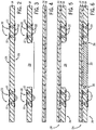
- FIGS. 2-10 a technique for manufacturing each of a plurality of buried die modules 10 is set forth, according to an embodiment of the invention.
- a cross-section of a singular buried die module build-up process is shown in each of FIGS. 2-10 for ease of visualization of the build-up process.
- the buried die module build-up process begins with the providing and patterning of an un-cut initial or "center" laminate flex layer 18.
- the initial laminate flex layer 18 is in the form of a Kapton® laminate flex, although as referenced above, other suitable materials may also be employed, such as Ultem®, polytetrafluoroethylene (PTFE), or another polymer film, such as a liquid crystal polymer (LCP) or a polyimide material.
- the initial laminate flex layer 18 has a thickness of around 50 micrometers in order to accommodate positioning of an ultrathin die in an opening formed therein, as will be explained in detail below.
- a plurality of vias 20 is formed through the laminate layer.
- the vias 20 are formed by way of a laser ablation or laser drilling process.
- vias 20 may be formed by way of other methods including: plasma etching, photo-definition, or mechanical drilling processes.
- a metal layer/material e.g., a seed metal and/or copper
- a sputtering, electroplating, and/or electro-less application process is then formed into metal interconnects 22.
- the metal layer/material is patterned and etched such that metal interconnects 22 are formed that extend through vias 20 and form interconnects 22 on each of a first surface 24 of initial laminate flex layer 18 and a second surface 26 of initial laminate flex layer 18.
- the initial laminate flex layer 18 may be provided as a "pre-patterned" layer having the plurality of vias 20 and the plurality of metal interconnects 22 already formed thereon/therein.
- a die opening 28 is formed in the initial laminate flex layer 18.
- the die opening 28 is of a size and shape essentially matching that of a die (i.e., die 30 in FIG. 6 ) to be placed therein, with the opening 28 being slightly oversized to accommodate receiving of the die therein.
- the resulting shape of the initial laminate flex layer 18 is that of a "window frame" construction.
- the opening 28 may be formed by one of a laser cutting and a die punch operation.
- the buried die module build-up process continues with the providing of an uncut laminate flex layer 32 having an adhesive material/layer 34 coated or applied thereto on a side to be joined to initial laminate flex layer 18.
- the uncut laminate flex layer 32 is a blank or unpatterned laminate flex.
- the uncut laminate flex layer 32 is positioned on (i.e., laminated onto) the first surface 24 of initial laminate flex layer 18 and secured thereto by way of the adhesive 34, as shown in FIG. 5 , with the uncut laminate flex layer 32 covering one side of the die opening 28 formed in initial laminate flex layer 18.
- the uncut laminate flex layer 32 is applied to the initial laminate flex layer 18 by way of a vacuum lamination, with the vacuum lamination being performed at a temperature that prevents curing of the adhesive material 34.
- a die 30 Upon placement of uncut laminate flex layer 32 onto initial laminate flex layer 18, a die 30 is positioned within die opening 28 formed in initial laminate flex layer 18, as shown in FIG. 6 .
- the die 30 is secured within opening 28 by way of the adhesive material 34 applied to uncut laminate flex layer 32.
- the die 30 is in the form of an "ultrathin die" that has a thickness equal to or matching that of initial laminate flex layer 18.
- each of the initial laminate flex layer 18 and the die 30 can be constructed to have a matching thickness of around 50 micrometers.
- an open/void moated region 36 remains present between die 30 and initial laminate flex layer 18.
- the vacuum lamination step that is performed to secure uncut laminate flex layer 32 to initial laminate flex layer 18 also acts to eliminate (at least partially) the void that is present in moated region 36. That is, in performing the vacuum lamination, adhesive material 34 is drawn into the moated region 36 to at least partially eliminate/fill the moated region.
- the buried die module build-up process continues with the providing of another uncut laminate flex layer 38 that is applied onto the second surface 26 of initial laminate flex layer 18 and onto the surface of the die 30 that is still exposed, as shown in FIG. 7 .
- the uncut laminate flex layer 38 is a blank or unpatterned laminate flex and is positioned on (i.e., laminated onto) initial laminate flex layer 18 and is secured thereto by way of an adhesive material/layer 34.
- a vacuum lamination (i.e., vacuum baking) step is performed to secure uncut laminate flex layer 38 to initial laminate flex layer 18.
- the vacuum lamination also functions to eliminate/fill (at least partially) the void that is present in moated region 36 between the die 30 and initial laminate flex layer 18, by drawing adhesive material 34 into the moated region 36 to at least partially eliminate the void therein and fill the moated region. As previously indicated, this vacuum lamination is performed at a temperature that prevents curing of the adhesive material 34.
- a curing of the adhesive layers 34 is performed.
- the curing is accomplished by way of a pressure baking operation, although it is recognized that other suitable curing processes could be employed.
- only a single baking/curing step is performed to cure both adhesive layers 34, therefore reducing processing time and costs associated with the build-up of the buried die module.
- the uncut laminate flex layers 32, 38 are patterned to form a plurality of vias 20, with the vias being drilled through the laminate flex layers 32, 38.
- the vias 20 are formed at positions corresponding to metal interconnects 22 formed on initial re-distribution layer 18, so as to expose the metal interconnects 22. Additional vias 20 are drilled down to pads 40 on die 30, so as to expose these pads.
- the vias 20 are formed by way of a laser ablation or laser drilling process.
- vias 20 may be formed by way of other methods including: plasma etching, photo-definition, or mechanical drilling processes.
- a metal layer/material (e.g., a seed metal and/or copper) is then applied onto the uncut laminate flex layers 32, 38 by way of, for example, a sputtering or electroplating process, and is then formed into metal interconnects 22.
- the metal layer/material is patterned and etched such that metal interconnects 22 are formed that extend from outward facing surfaces 42 of laminate flex layers 32, 38 and down through vias 20.
- the metal interconnects 22 on laminate flex layers 32, 38 thus form an electrical connection with interconnects 22 on initial laminate flex layer 18 and a direct metallic and electrical connection to die pads 40.
- the vias 20 are formed (i.e., drilled, laser ablated) from a first direction 44. That is, vias 20 in the uncut laminate flex layer 32 are formed from the top-down.
- the vias 20 are drilled from a second direction 46 that is opposite of the first direction 44. That is, vias 20 in the uncut laminate flex layer 38 are drilled from the bottom-up.
- additional uncut laminate flex layers 48, 50 are laminated onto the uncut laminate flex layers 32, 38 and are subsequently patterned.
- the additional laminate flex layers 48, 50 are in the form of uncut laminate flex layers that are applied to opposing surfaces of the buried die module by way of an adhesive material 51, so as to form a balanced buried die module with equal numbers of laminate flex layers extending out from initial laminate flex layer 18. That is, the initial laminate flex layer 18 forms a "central" laminate flex layer, and the additional laminate flex layers 48, 50 are applied on opposing sides of the initial laminate flex layer 18 (i.e., on both the first and second surfaces 24, 26 of initial laminate flex layer 18).
- Such a double-sided lamination process serves to reduce stresses imparted to the initial laminate flex layer 18 and prevent warpage thereof.
- a plurality of vias 20 is formed in each of the additional laminate flex layers 48, 50.
- Metal interconnects 22 are also formed/patterned to extend down through vias 20 and through the additional laminate flex layer 48, 50, so as to electrically connect each of the additional laminate flex layers 48, 50 to the adjacent uncut laminate flex layers 32, 38. Similar to the patterning of laminate flex layers 32, 38, the patterning of additional laminate flex layers 48, 50 is performed according to a double-sided patterning process.
- the vias 20 formed in laminate flex layer 48 are drilled/laser ablated from first direction 44 (i.e., from the top-down), while the vias 20 formed in laminate flex layer 50 are drilled/laser ablated from second direction 46 (i.e., from the bottom-up).
- a solder mask layer 52 is applied to outermost laminate flex layers 48, 50 on opposing surfaces of the buried die module.
- the solder mask 52 provides for connection of a separate package/module to the buried die module.
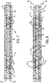
- a ball grid array (BGA) package 54 is assembled to or stacked on the buried die module 10.
- a separate buried die module 56 is stacked onto buried die module 10.
- the stacked buried die modules 10, 56 are coupled together by way of a ball grid array 58, although it is recognized that a land grid array or conductive epoxy, for example, could also be used to couple the modules together. While FIG. 12 shows a stacking of two buried die modules 10, 56 in a vertical arrangement, it is recognized that a still greater number of buried die modules could be stacked on one another.
- a buried die module 60 that includes a first die 62 and a second die 64 that are arranged/applied in a common horizontal plane.
- each of the first and second dies 62, 64 has a thickness matching that of initial laminate flex layer 66.
- Each of the first and second dies 62, 64 are placed within separate die openings 68, 70 formed in initial laminate flex layer 66, so as to be arranged in the same horizontal plane.
- a plurality of vias 20 and metal interconnects 22 that extend down through vias 20 are patterned in adjacent uncut laminate flex layers 72, 74 such that metal interconnects extend to pads 76 on each of first and second dies 62, 64. That is, metal interconnects 22 extend down to pads 76 to form a direct metallic and electrical connection to die pads 76 of first and second dies 62, 64.
- the side-by-side embedding of first and second dies 62, 64 on the same plane i.e. laminate flex layer 66), allows for a reduction in the number of laminate flex layers in the buried die module 60, thus helping to reduce overall thickness of the buried die module 60 and reduce associated production costs.
- embodiments of the invention thus provide a buried die module build-up process having a shorter manufacturing cycle time and that allows for the application of multiple laminate layers while minimizing warpage of the module without the use of a stiffener.
- the build-up process combines the curing of multiple adhesive layers (via multiple curing steps) into a single curing step, so as to reduce processing time and costs associated therewith, and employs vacuum lamination steps for complete removal of all voids around the die, with the moated region around the die being completely filled.
- the build-up process provides a module that is completely balanced, based on the double-sided lamination and via formation processes included therein and based on the use of an identical adhesive on both sides of the buried die.
- the finished buried die module resulting from the build-up process is very thin and is compatible with additional buried die modules, so as to provide for the formation of stacked die modules.
- buried die modules can thus be constructed having a reduced thickness, controlled flatness, improved design density, increased resolution, and improved electrical performance over other existing buried die module build-up techniques.
- a method of forming a buried die module includes providing an initial laminate flex layer and forming a plurality of vias and a plurality of metal interconnects in and on the initial laminate flex layer, the plurality of metal interconnects extending through respective vias so as to form interconnects on each of opposing first and second surfaces of the initial laminate flex layer, forming a die opening through the initial laminate flex layer.
- the method also includes securing a first uncut laminate flex layer to the first surface of the initial laminate flex layer by way of an adhesive material, positioning a die within the die opening of the initial laminate flex layer and onto the adhesive material, securing a second uncut laminate flex layer to the second surface of the initial laminate flex layer by way of an adhesive material, curing the adhesive material between the first uncut laminate flex layer and the initial laminate flex layer and between the second uncut laminate flex layer and the initial laminate flex layer, and forming a plurality of vias and a plurality of metal interconnects in and on the first and second uncut laminate flex layers, each of the plurality of metal interconnects extending through a respective via and being directly metalized to one of a metal interconnect on the initial laminate flex layer and a die pad on the die.
- a method of forming an embedded chip package includes forming a plurality of vias in a center laminate layer, forming a plurality of metal interconnects that extend through the plurality of vias so as to form interconnects on each of opposing first and second surfaces of the center laminate layer, forming a chip opening through the center laminate layer, applying a first uncut laminate layer to the first surface of the center laminate layer by way of an adhesive material, and positioning a chip within the chip opening of the center laminate layer and onto the adhesive material, the chip having a thickness equal to a thickness of the center laminate layer.
- the method also includes applying a second uncut laminate layer to the second surface of the center laminate layer by way of an adhesive material, curing the adhesive material between the first uncut laminate layer and the center laminate layer and between the second uncut laminate layer and the center laminate layer, and patterning the first and second uncut laminate layers to form a plurality of vias and a plurality of metal interconnects such that each of the plurality of metal interconnects extends through a respective via and is directly metalized to one of a metal interconnect on the center laminate layer and a chip pad on the chip.
- an embedded chip package is manufactured by a process that includes the step of pre-patterning a center laminate layer to form a plurality of vias and a plurality of metal interconnects that extend through the plurality of vias, wherein the plurality of metal interconnects form interconnects on each of opposing first and second surfaces of the center laminate layer.
- the process also includes forming a die opening through the center laminate layer, applying a first uncut laminate layer to the first surface of the center laminate layer by way of an adhesive material, positioning a die within the die opening of the center laminate layer and onto the adhesive material, the die having a thickness equal to a thickness of the center laminate layer, applying a second uncut laminate layer to the second surface of the center laminate layer by way of an adhesive material, curing the adhesive material between the first uncut laminate flex layer and the base laminate flex layer and between the second uncut laminate flex layer and the base laminate flex layer together at the same time, and performing a double-sided patterning the first and second uncut laminate flex layers to form a plurality of vias and a plurality of metal interconnects, wherein the plurality of vias and the plurality of metal interconnects of the first uncut laminate flex layer are formed from a first direction and the plurality of vias and the plurality of metal interconnects of the second uncut laminate flex layer are formed from a second direction that is opposite the first direction
Landscapes
- Engineering & Computer Science (AREA)
- Microelectronics & Electronic Packaging (AREA)
- Manufacturing & Machinery (AREA)
- Production Of Multi-Layered Print Wiring Board (AREA)
- Physics & Mathematics (AREA)
- Geometry (AREA)
Applications Claiming Priority (1)
| Application Number | Priority Date | Filing Date | Title |
|---|---|---|---|
| US13/431,168 US8658473B2 (en) | 2012-03-27 | 2012-03-27 | Ultrathin buried die module and method of manufacturing thereof |
Publications (3)
| Publication Number | Publication Date |
|---|---|
| EP2672789A2 EP2672789A2 (en) | 2013-12-11 |
| EP2672789A3 EP2672789A3 (en) | 2017-11-22 |
| EP2672789B1 true EP2672789B1 (en) | 2020-03-18 |
Family
ID=47997208
Family Applications (1)
| Application Number | Title | Priority Date | Filing Date |
|---|---|---|---|
| EP13161463.8A Active EP2672789B1 (en) | 2012-03-27 | 2013-03-27 | Ultrathin buried die module and method of manufacturing thereof |
Country Status (7)
| Country | Link |
|---|---|
| US (2) | US8658473B2 (https=) |
| EP (1) | EP2672789B1 (https=) |
| JP (1) | JP6342120B2 (https=) |
| KR (1) | KR102071522B1 (https=) |
| CN (2) | CN108109982A (https=) |
| SG (1) | SG193756A1 (https=) |
| TW (1) | TWI593030B (https=) |
Families Citing this family (31)
| Publication number | Priority date | Publication date | Assignee | Title |
|---|---|---|---|---|
| US8658473B2 (en) * | 2012-03-27 | 2014-02-25 | General Electric Company | Ultrathin buried die module and method of manufacturing thereof |
| KR20150074785A (ko) * | 2013-12-24 | 2015-07-02 | 삼성전기주식회사 | 빌드업 절연필름, 그를 이용한 전자부품 내장형 인쇄회로기판 및 그 제조방법 |
| US9806051B2 (en) * | 2014-03-04 | 2017-10-31 | General Electric Company | Ultra-thin embedded semiconductor device package and method of manufacturing thereof |
| US9930793B2 (en) | 2014-03-27 | 2018-03-27 | Intel Corporation | Electric circuit on flexible substrate |
| US9601353B2 (en) * | 2014-07-30 | 2017-03-21 | Taiwan Semiconductor Manufacturing Company, Ltd. | Packages with molding structures and methods of forming the same |
| US9653438B2 (en) * | 2014-08-21 | 2017-05-16 | General Electric Company | Electrical interconnect structure for an embedded semiconductor device package and method of manufacturing thereof |
| US10192846B2 (en) | 2014-11-05 | 2019-01-29 | Infineon Technologies Austria Ag | Method of inserting an electronic component into a slot in a circuit board |
| US10553557B2 (en) | 2014-11-05 | 2020-02-04 | Infineon Technologies Austria Ag | Electronic component, system and method |
| US10064287B2 (en) | 2014-11-05 | 2018-08-28 | Infineon Technologies Austria Ag | System and method of providing a semiconductor carrier and redistribution structure |
| JP2016219477A (ja) * | 2015-05-15 | 2016-12-22 | イビデン株式会社 | 電子部品内蔵配線板及びその製造方法 |
| JP2017017238A (ja) * | 2015-07-03 | 2017-01-19 | 株式会社ジェイデバイス | 半導体装置及びその製造方法 |
| JP6438370B2 (ja) * | 2015-08-03 | 2018-12-12 | Jx金属株式会社 | プリント配線板の製造方法、表面処理銅箔、積層体、プリント配線板、半導体パッケージ及び電子機器 |
| WO2017022807A1 (ja) * | 2015-08-03 | 2017-02-09 | Jx金属株式会社 | プリント配線板の製造方法、表面処理銅箔、積層体、プリント配線板、半導体パッケージ及び電子機器 |
| KR102384863B1 (ko) * | 2015-09-09 | 2022-04-08 | 삼성전자주식회사 | 반도체 칩 패키지 및 이의 제조 방법 |
| EP3206229B1 (en) * | 2016-02-09 | 2020-10-07 | AT & S Austria Technologie & Systemtechnik Aktiengesellschaft | Methods of manufacturing flexible electronic devices |
| CN107295746B (zh) * | 2016-03-31 | 2021-06-15 | 奥特斯(中国)有限公司 | 器件载体及其制造方法 |
| US20170373011A1 (en) * | 2016-06-28 | 2017-12-28 | General Electric Company | Semiconductor die backside devices and methods of fabrication thereof |
| KR102566996B1 (ko) * | 2016-09-09 | 2023-08-14 | 삼성전자주식회사 | FOWLP 형태의 반도체 패키지 및 이를 가지는 PoP 형태의 반도체 패키지 |
| KR101994748B1 (ko) | 2016-09-12 | 2019-07-01 | 삼성전기주식회사 | 팬-아웃 반도체 패키지 |
| CN106876291B (zh) * | 2016-12-30 | 2020-04-10 | 清华大学 | 一种薄芯片柔性扇出封装方法及所制备的封装结构 |
| CN106711053B (zh) * | 2016-12-30 | 2019-09-17 | 清华大学 | 薄芯片柔性封装方法及所制备的封装结构 |
| US11830848B2 (en) | 2016-12-31 | 2023-11-28 | Intel Corporation | Electronic device package |
| TWI648854B (zh) * | 2017-06-14 | 2019-01-21 | Win Semiconductors Corp. | 用以減少化合物半導體晶圓變形之改良結構 |
| EP3557608A1 (en) * | 2018-04-19 | 2019-10-23 | AT & S Austria Technologie & Systemtechnik Aktiengesellschaft | Packaged integrated circuit with interposing functionality and method for manufacturing such a packaged integrated circuit |
| US11227841B2 (en) * | 2018-06-28 | 2022-01-18 | Intel Corporation | Stiffener build-up layer package |
| DE102019117844A1 (de) * | 2018-09-27 | 2020-04-02 | Taiwan Semiconductor Manufacturing Co., Ltd. | Integrierte-schaltung-package und verfahren |
| US20200161206A1 (en) | 2018-11-20 | 2020-05-21 | Advanced Semiconductor Engineering, Inc. | Semiconductor package structure and semiconductor manufacturing process |
| CN110957269A (zh) * | 2019-11-08 | 2020-04-03 | 广东佛智芯微电子技术研究有限公司 | 一种改善埋入式扇出型封装结构电镀性能的制作方法 |
| WO2022055405A1 (en) * | 2020-09-10 | 2022-03-17 | Smoltek Ab | Electronic component package with integrated component and redistribution layer stack |
| CN115132670A (zh) * | 2021-03-24 | 2022-09-30 | 浙江荷清柔性电子技术有限公司 | 一种集成封装方法、柔性层叠基板及柔性电路结构 |
| CN116994964A (zh) * | 2022-04-25 | 2023-11-03 | 宏启胜精密电子(秦皇岛)有限公司 | 封装结构及其制备方法 |
Family Cites Families (46)
| Publication number | Priority date | Publication date | Assignee | Title |
|---|---|---|---|---|
| US5353498A (en) | 1993-02-08 | 1994-10-11 | General Electric Company | Method for fabricating an integrated circuit module |
| US5567657A (en) | 1995-12-04 | 1996-10-22 | General Electric Company | Fabrication and structures of two-sided molded circuit modules with flexible interconnect layers |
| US5841193A (en) * | 1996-05-20 | 1998-11-24 | Epic Technologies, Inc. | Single chip modules, repairable multichip modules, and methods of fabrication thereof |
| JP3051700B2 (ja) | 1997-07-28 | 2000-06-12 | 京セラ株式会社 | 素子内蔵多層配線基板の製造方法 |
| JP3798597B2 (ja) | 1999-11-30 | 2006-07-19 | 富士通株式会社 | 半導体装置 |
| US20020020898A1 (en) | 2000-08-16 | 2002-02-21 | Vu Quat T. | Microelectronic substrates with integrated devices |
| JP2002164475A (ja) * | 2000-11-24 | 2002-06-07 | Nitto Denko Corp | 半導体装置 |
| JP2002246745A (ja) | 2001-02-14 | 2002-08-30 | Ibiden Co Ltd | 三次元実装パッケージ及びその製造方法、三次元実装パッケージ製造用接着材 |
| JP4694007B2 (ja) | 2001-02-14 | 2011-06-01 | イビデン株式会社 | 三次元実装パッケージの製造方法 |
| JP2002270712A (ja) | 2001-03-14 | 2002-09-20 | Sony Corp | 半導体素子内蔵多層配線基板と半導体素子内蔵装置、およびそれらの製造方法 |
| US6706553B2 (en) * | 2001-03-26 | 2004-03-16 | Intel Corporation | Dispensing process for fabrication of microelectronic packages |
| US7332819B2 (en) | 2002-01-09 | 2008-02-19 | Micron Technology, Inc. | Stacked die in die BGA package |
| US20030116860A1 (en) | 2001-12-21 | 2003-06-26 | Biju Chandran | Semiconductor package with low resistance package-to-die interconnect scheme for reduced die stresses |
| JP2003234432A (ja) | 2002-02-08 | 2003-08-22 | Ibiden Co Ltd | 半導体チップ実装回路基板および多層化回路基板 |
| EP2866258B1 (en) | 2002-05-31 | 2019-04-17 | Socionext Inc. | Semiconductor device and manufacturing method thereof |
| TWI251916B (en) | 2003-08-28 | 2006-03-21 | Phoenix Prec Technology Corp | Semiconductor assembled heat sink structure for embedding electronic components |
| JP2005317903A (ja) | 2004-03-31 | 2005-11-10 | Alps Electric Co Ltd | 回路部品モジュール、回路部品モジュールスタック、記録媒体およびこれらの製造方法 |
| DE102004041889B4 (de) | 2004-08-30 | 2006-06-29 | Infineon Technologies Ag | Halbleitervorrichtung mit gestapelten Halbleiterbauelementen und Verfahren zu deren Herstellung |
| KR100688768B1 (ko) * | 2004-12-30 | 2007-03-02 | 삼성전기주식회사 | 칩 내장형 인쇄회로기판 및 그 제조 방법 |
| KR100716815B1 (ko) * | 2005-02-28 | 2007-05-09 | 삼성전기주식회사 | 칩 내장형 인쇄회로기판 및 그 제조방법 |
| TWI261329B (en) | 2005-03-09 | 2006-09-01 | Phoenix Prec Technology Corp | Conductive bump structure of circuit board and method for fabricating the same |
| US7640655B2 (en) | 2005-09-13 | 2010-01-05 | Shinko Electric Industries Co., Ltd. | Electronic component embedded board and its manufacturing method |
| KR100700922B1 (ko) * | 2005-10-17 | 2007-03-28 | 삼성전기주식회사 | 수동 소자를 내장한 기판 및 그 제조 방법 |
| KR100796523B1 (ko) * | 2006-08-17 | 2008-01-21 | 삼성전기주식회사 | 전자부품 내장형 다층 인쇄배선기판 및 그 제조방법 |
| JP2008085310A (ja) * | 2006-08-28 | 2008-04-10 | Clover Denshi Kogyo Kk | 多層プリント配線基板 |
| US7504283B2 (en) * | 2006-12-18 | 2009-03-17 | Texas Instruments Incorporated | Stacked-flip-assembled semiconductor chips embedded in thin hybrid substrate |
| TWI330401B (en) * | 2006-12-25 | 2010-09-11 | Unimicron Technology Corp | Circuit board structure having embedded semiconductor component and fabrication method thereof |
| US20080318413A1 (en) | 2007-06-21 | 2008-12-25 | General Electric Company | Method for making an interconnect structure and interconnect component recovery process |
| US7863090B2 (en) * | 2007-06-25 | 2011-01-04 | Epic Technologies, Inc. | Packaged electronic modules and fabrication methods thereof implementing a cell phone or other electronic system |
| SG148901A1 (en) | 2007-07-09 | 2009-01-29 | Micron Technology Inc | Packaged semiconductor assemblies and methods for manufacturing such assemblies |
| KR100885924B1 (ko) | 2007-08-10 | 2009-02-26 | 삼성전자주식회사 | 묻혀진 도전성 포스트를 포함하는 반도체 패키지 및 그제조방법 |
| US8039303B2 (en) * | 2008-06-11 | 2011-10-18 | Stats Chippac, Ltd. | Method of forming stress relief layer between die and interconnect structure |
| US8114708B2 (en) * | 2008-09-30 | 2012-02-14 | General Electric Company | System and method for pre-patterned embedded chip build-up |
| US8008125B2 (en) * | 2009-03-06 | 2011-08-30 | General Electric Company | System and method for stacked die embedded chip build-up |
| TWI399140B (zh) * | 2009-06-12 | 2013-06-11 | 欣興電子股份有限公司 | 內埋式封裝結構的製作方法 |
| JP2011014728A (ja) * | 2009-07-02 | 2011-01-20 | Casio Computer Co Ltd | 半導体装置及び半導体装置の製造方法 |
| JP5280309B2 (ja) * | 2009-07-17 | 2013-09-04 | 新光電気工業株式会社 | 半導体装置及びその製造方法 |
| WO2011058879A1 (ja) * | 2009-11-12 | 2011-05-19 | 日本電気株式会社 | 機能素子内蔵基板、機能素子内蔵基板の製造方法、及び、配線基板 |
| US8742561B2 (en) * | 2009-12-29 | 2014-06-03 | Intel Corporation | Recessed and embedded die coreless package |
| JP5001395B2 (ja) * | 2010-03-31 | 2012-08-15 | イビデン株式会社 | 配線板及び配線板の製造方法 |
| US9262015B2 (en) | 2010-06-28 | 2016-02-16 | Intel Corporation | System for portable tangible interaction |
| US8653670B2 (en) * | 2010-06-29 | 2014-02-18 | General Electric Company | Electrical interconnect for an integrated circuit package and method of making same |
| US8623699B2 (en) * | 2010-07-26 | 2014-01-07 | General Electric Company | Method of chip package build-up |
| US8304913B2 (en) * | 2010-09-24 | 2012-11-06 | Intel Corporation | Methods of forming fully embedded bumpless build-up layer packages and structures formed thereby |
| US8384227B2 (en) * | 2010-11-16 | 2013-02-26 | Stats Chippac, Ltd. | Semiconductor device and method of forming interposer frame electrically connected to embedded semiconductor die |
| US8658473B2 (en) * | 2012-03-27 | 2014-02-25 | General Electric Company | Ultrathin buried die module and method of manufacturing thereof |
-
2012
- 2012-03-27 US US13/431,168 patent/US8658473B2/en not_active Expired - Fee Related
-
2013
- 2013-03-14 TW TW102109110A patent/TWI593030B/zh active
- 2013-03-21 JP JP2013057468A patent/JP6342120B2/ja active Active
- 2013-03-22 KR KR1020130031093A patent/KR102071522B1/ko active Active
- 2013-03-26 SG SG2013022314A patent/SG193756A1/en unknown
- 2013-03-27 CN CN201810053234.0A patent/CN108109982A/zh active Pending
- 2013-03-27 CN CN201310101675.0A patent/CN103367169B/zh active Active
- 2013-03-27 EP EP13161463.8A patent/EP2672789B1/en active Active
-
2014
- 2014-02-24 US US14/188,093 patent/US9236348B2/en active Active
Also Published As
| Publication number | Publication date |
|---|---|
| TW201349364A (zh) | 2013-12-01 |
| US8658473B2 (en) | 2014-02-25 |
| TWI593030B (zh) | 2017-07-21 |
| EP2672789A2 (en) | 2013-12-11 |
| CN103367169B (zh) | 2018-02-27 |
| US9236348B2 (en) | 2016-01-12 |
| CN103367169A (zh) | 2013-10-23 |
| KR102071522B1 (ko) | 2020-03-02 |
| JP2013243345A (ja) | 2013-12-05 |
| KR20130110052A (ko) | 2013-10-08 |
| SG193756A1 (en) | 2013-10-30 |
| JP6342120B2 (ja) | 2018-06-13 |
| US20140183750A1 (en) | 2014-07-03 |
| CN108109982A (zh) | 2018-06-01 |
| US20130256900A1 (en) | 2013-10-03 |
| EP2672789A3 (en) | 2017-11-22 |
Similar Documents
| Publication | Publication Date | Title |
|---|---|---|
| EP2672789B1 (en) | Ultrathin buried die module and method of manufacturing thereof | |
| US8008125B2 (en) | System and method for stacked die embedded chip build-up | |
| JP2013243345A5 (https=) | ||
| EP2402992B1 (en) | Method of fabricating an embedded chip package | |
| JP5588620B2 (ja) | ウェーハ・レベル・パッケージ及びその形成方法 | |
| JP2013030593A (ja) | 半導体装置、該半導体装置を垂直に積層した半導体モジュール構造及びその製造方法 | |
| TW201325343A (zh) | 用於嵌入式晶粒封裝的高精密度自我對準晶粒 | |
| US9570376B2 (en) | Electrical interconnect for an integrated circuit package and method of making same | |
| US9730329B2 (en) | Active chip package substrate and method for preparing the same | |
| JP6034664B2 (ja) | 半導体装置、半導体積層モジュール構造、積層モジュール構造、及びこれらの製造方法 | |
| US20140097545A1 (en) | Package structure and method for manufacturing package structure |
Legal Events
| Date | Code | Title | Description |
|---|---|---|---|
| PUAI | Public reference made under article 153(3) epc to a published international application that has entered the european phase |
Free format text: ORIGINAL CODE: 0009012 |
|
| AK | Designated contracting states |
Kind code of ref document: A2 Designated state(s): AL AT BE BG CH CY CZ DE DK EE ES FI FR GB GR HR HU IE IS IT LI LT LU LV MC MK MT NL NO PL PT RO RS SE SI SK SM TR |
|
| AX | Request for extension of the european patent |
Extension state: BA ME |
|
| PUAL | Search report despatched |
Free format text: ORIGINAL CODE: 0009013 |
|
| RIC1 | Information provided on ipc code assigned before grant |
Ipc: H01L 21/56 20060101ALI20171011BHEP Ipc: H05K 3/46 20060101ALI20171011BHEP Ipc: H01L 23/538 20060101ALN20171011BHEP Ipc: H01L 25/10 20060101ALI20171011BHEP Ipc: H01L 23/522 20060101ALI20171011BHEP Ipc: H01L 23/00 20060101ALI20171011BHEP Ipc: H05K 1/02 20060101AFI20171011BHEP Ipc: H01L 21/60 20060101ALN20171011BHEP Ipc: H05K 1/18 20060101ALI20171011BHEP Ipc: H01L 21/48 20060101ALI20171011BHEP Ipc: H01L 23/48 20060101ALI20171011BHEP Ipc: H01L 23/498 20060101ALI20171011BHEP Ipc: H01L 23/31 20060101ALI20171011BHEP Ipc: H05K 1/14 20060101ALN20171011BHEP |
|
| AK | Designated contracting states |
Kind code of ref document: A3 Designated state(s): AL AT BE BG CH CY CZ DE DK EE ES FI FR GB GR HR HU IE IS IT LI LT LU LV MC MK MT NL NO PL PT RO RS SE SI SK SM TR |
|
| AX | Request for extension of the european patent |
Extension state: BA ME |
|
| STAA | Information on the status of an ep patent application or granted ep patent |
Free format text: STATUS: REQUEST FOR EXAMINATION WAS MADE |
|
| 17P | Request for examination filed |
Effective date: 20180522 |
|
| RBV | Designated contracting states (corrected) |
Designated state(s): AL AT BE BG CH CY CZ DE DK EE ES FI FR GB GR HR HU IE IS IT LI LT LU LV MC MK MT NL NO PL PT RO RS SE SI SK SM TR |
|
| REG | Reference to a national code |
Ref country code: DE Ref legal event code: R079 Ref document number: 602013066874 Country of ref document: DE Free format text: PREVIOUS MAIN CLASS: H05K0001180000 Ipc: H05K0001020000 |
|
| GRAP | Despatch of communication of intention to grant a patent |
Free format text: ORIGINAL CODE: EPIDOSNIGR1 |
|
| STAA | Information on the status of an ep patent application or granted ep patent |
Free format text: STATUS: GRANT OF PATENT IS INTENDED |
|
| RIC1 | Information provided on ipc code assigned before grant |
Ipc: H01L 21/48 20060101ALI20191015BHEP Ipc: H01L 23/31 20060101ALI20191015BHEP Ipc: H01L 25/10 20060101ALI20191015BHEP Ipc: H01L 23/498 20060101ALI20191015BHEP Ipc: H01L 23/00 20060101ALI20191015BHEP Ipc: H01L 21/60 20060101ALN20191015BHEP Ipc: H05K 1/18 20060101ALI20191015BHEP Ipc: H05K 1/14 20060101ALN20191015BHEP Ipc: H01L 23/538 20060101ALN20191015BHEP Ipc: H01L 23/522 20060101ALI20191015BHEP Ipc: H01L 21/56 20060101ALI20191015BHEP Ipc: H05K 1/02 20060101AFI20191015BHEP Ipc: H05K 3/46 20060101ALI20191015BHEP Ipc: H01L 23/48 20060101ALI20191015BHEP |
|
| INTG | Intention to grant announced |
Effective date: 20191108 |
|
| GRAS | Grant fee paid |
Free format text: ORIGINAL CODE: EPIDOSNIGR3 |
|
| GRAA | (expected) grant |
Free format text: ORIGINAL CODE: 0009210 |
|
| STAA | Information on the status of an ep patent application or granted ep patent |
Free format text: STATUS: THE PATENT HAS BEEN GRANTED |
|
| AK | Designated contracting states |
Kind code of ref document: B1 Designated state(s): AL AT BE BG CH CY CZ DE DK EE ES FI FR GB GR HR HU IE IS IT LI LT LU LV MC MK MT NL NO PL PT RO RS SE SI SK SM TR |
|
| REG | Reference to a national code |
Ref country code: GB Ref legal event code: FG4D |
|
| REG | Reference to a national code |
Ref country code: DE Ref legal event code: R096 Ref document number: 602013066874 Country of ref document: DE |
|
| REG | Reference to a national code |
Ref country code: AT Ref legal event code: REF Ref document number: 1247420 Country of ref document: AT Kind code of ref document: T Effective date: 20200415 Ref country code: IE Ref legal event code: FG4D |
|
| PG25 | Lapsed in a contracting state [announced via postgrant information from national office to epo] |
Ref country code: RS Free format text: LAPSE BECAUSE OF FAILURE TO SUBMIT A TRANSLATION OF THE DESCRIPTION OR TO PAY THE FEE WITHIN THE PRESCRIBED TIME-LIMIT Effective date: 20200318 Ref country code: FI Free format text: LAPSE BECAUSE OF FAILURE TO SUBMIT A TRANSLATION OF THE DESCRIPTION OR TO PAY THE FEE WITHIN THE PRESCRIBED TIME-LIMIT Effective date: 20200318 Ref country code: NO Free format text: LAPSE BECAUSE OF FAILURE TO SUBMIT A TRANSLATION OF THE DESCRIPTION OR TO PAY THE FEE WITHIN THE PRESCRIBED TIME-LIMIT Effective date: 20200618 |
|
| REG | Reference to a national code |
Ref country code: NL Ref legal event code: MP Effective date: 20200318 |
|
| PG25 | Lapsed in a contracting state [announced via postgrant information from national office to epo] |
Ref country code: HR Free format text: LAPSE BECAUSE OF FAILURE TO SUBMIT A TRANSLATION OF THE DESCRIPTION OR TO PAY THE FEE WITHIN THE PRESCRIBED TIME-LIMIT Effective date: 20200318 Ref country code: GR Free format text: LAPSE BECAUSE OF FAILURE TO SUBMIT A TRANSLATION OF THE DESCRIPTION OR TO PAY THE FEE WITHIN THE PRESCRIBED TIME-LIMIT Effective date: 20200619 Ref country code: SE Free format text: LAPSE BECAUSE OF FAILURE TO SUBMIT A TRANSLATION OF THE DESCRIPTION OR TO PAY THE FEE WITHIN THE PRESCRIBED TIME-LIMIT Effective date: 20200318 Ref country code: LV Free format text: LAPSE BECAUSE OF FAILURE TO SUBMIT A TRANSLATION OF THE DESCRIPTION OR TO PAY THE FEE WITHIN THE PRESCRIBED TIME-LIMIT Effective date: 20200318 Ref country code: BG Free format text: LAPSE BECAUSE OF FAILURE TO SUBMIT A TRANSLATION OF THE DESCRIPTION OR TO PAY THE FEE WITHIN THE PRESCRIBED TIME-LIMIT Effective date: 20200618 |
|
| REG | Reference to a national code |
Ref country code: LT Ref legal event code: MG4D |
|
| PG25 | Lapsed in a contracting state [announced via postgrant information from national office to epo] |
Ref country code: NL Free format text: LAPSE BECAUSE OF FAILURE TO SUBMIT A TRANSLATION OF THE DESCRIPTION OR TO PAY THE FEE WITHIN THE PRESCRIBED TIME-LIMIT Effective date: 20200318 |
|
| PG25 | Lapsed in a contracting state [announced via postgrant information from national office to epo] |
Ref country code: CZ Free format text: LAPSE BECAUSE OF FAILURE TO SUBMIT A TRANSLATION OF THE DESCRIPTION OR TO PAY THE FEE WITHIN THE PRESCRIBED TIME-LIMIT Effective date: 20200318 Ref country code: IS Free format text: LAPSE BECAUSE OF FAILURE TO SUBMIT A TRANSLATION OF THE DESCRIPTION OR TO PAY THE FEE WITHIN THE PRESCRIBED TIME-LIMIT Effective date: 20200718 Ref country code: SK Free format text: LAPSE BECAUSE OF FAILURE TO SUBMIT A TRANSLATION OF THE DESCRIPTION OR TO PAY THE FEE WITHIN THE PRESCRIBED TIME-LIMIT Effective date: 20200318 Ref country code: RO Free format text: LAPSE BECAUSE OF FAILURE TO SUBMIT A TRANSLATION OF THE DESCRIPTION OR TO PAY THE FEE WITHIN THE PRESCRIBED TIME-LIMIT Effective date: 20200318 Ref country code: PT Free format text: LAPSE BECAUSE OF FAILURE TO SUBMIT A TRANSLATION OF THE DESCRIPTION OR TO PAY THE FEE WITHIN THE PRESCRIBED TIME-LIMIT Effective date: 20200812 Ref country code: LT Free format text: LAPSE BECAUSE OF FAILURE TO SUBMIT A TRANSLATION OF THE DESCRIPTION OR TO PAY THE FEE WITHIN THE PRESCRIBED TIME-LIMIT Effective date: 20200318 Ref country code: EE Free format text: LAPSE BECAUSE OF FAILURE TO SUBMIT A TRANSLATION OF THE DESCRIPTION OR TO PAY THE FEE WITHIN THE PRESCRIBED TIME-LIMIT Effective date: 20200318 Ref country code: SM Free format text: LAPSE BECAUSE OF FAILURE TO SUBMIT A TRANSLATION OF THE DESCRIPTION OR TO PAY THE FEE WITHIN THE PRESCRIBED TIME-LIMIT Effective date: 20200318 |
|
| REG | Reference to a national code |
Ref country code: CH Ref legal event code: PL |
|
| REG | Reference to a national code |
Ref country code: AT Ref legal event code: MK05 Ref document number: 1247420 Country of ref document: AT Kind code of ref document: T Effective date: 20200318 |
|
| REG | Reference to a national code |
Ref country code: DE Ref legal event code: R097 Ref document number: 602013066874 Country of ref document: DE |
|
| REG | Reference to a national code |
Ref country code: BE Ref legal event code: MM Effective date: 20200331 |
|
| PG25 | Lapsed in a contracting state [announced via postgrant information from national office to epo] |
Ref country code: MC Free format text: LAPSE BECAUSE OF FAILURE TO SUBMIT A TRANSLATION OF THE DESCRIPTION OR TO PAY THE FEE WITHIN THE PRESCRIBED TIME-LIMIT Effective date: 20200318 Ref country code: LU Free format text: LAPSE BECAUSE OF NON-PAYMENT OF DUE FEES Effective date: 20200327 |
|
| PLBE | No opposition filed within time limit |
Free format text: ORIGINAL CODE: 0009261 |
|
| STAA | Information on the status of an ep patent application or granted ep patent |
Free format text: STATUS: NO OPPOSITION FILED WITHIN TIME LIMIT |
|
| PG25 | Lapsed in a contracting state [announced via postgrant information from national office to epo] |
Ref country code: DK Free format text: LAPSE BECAUSE OF FAILURE TO SUBMIT A TRANSLATION OF THE DESCRIPTION OR TO PAY THE FEE WITHIN THE PRESCRIBED TIME-LIMIT Effective date: 20200318 Ref country code: IE Free format text: LAPSE BECAUSE OF NON-PAYMENT OF DUE FEES Effective date: 20200327 Ref country code: ES Free format text: LAPSE BECAUSE OF FAILURE TO SUBMIT A TRANSLATION OF THE DESCRIPTION OR TO PAY THE FEE WITHIN THE PRESCRIBED TIME-LIMIT Effective date: 20200318 Ref country code: CH Free format text: LAPSE BECAUSE OF NON-PAYMENT OF DUE FEES Effective date: 20200331 Ref country code: LI Free format text: LAPSE BECAUSE OF NON-PAYMENT OF DUE FEES Effective date: 20200331 Ref country code: IT Free format text: LAPSE BECAUSE OF FAILURE TO SUBMIT A TRANSLATION OF THE DESCRIPTION OR TO PAY THE FEE WITHIN THE PRESCRIBED TIME-LIMIT Effective date: 20200318 Ref country code: AT Free format text: LAPSE BECAUSE OF FAILURE TO SUBMIT A TRANSLATION OF THE DESCRIPTION OR TO PAY THE FEE WITHIN THE PRESCRIBED TIME-LIMIT Effective date: 20200318 |
|
| 26N | No opposition filed |
Effective date: 20201221 |
|
| PG25 | Lapsed in a contracting state [announced via postgrant information from national office to epo] |
Ref country code: BE Free format text: LAPSE BECAUSE OF NON-PAYMENT OF DUE FEES Effective date: 20200331 Ref country code: PL Free format text: LAPSE BECAUSE OF FAILURE TO SUBMIT A TRANSLATION OF THE DESCRIPTION OR TO PAY THE FEE WITHIN THE PRESCRIBED TIME-LIMIT Effective date: 20200318 |
|
| PG25 | Lapsed in a contracting state [announced via postgrant information from national office to epo] |
Ref country code: SI Free format text: LAPSE BECAUSE OF FAILURE TO SUBMIT A TRANSLATION OF THE DESCRIPTION OR TO PAY THE FEE WITHIN THE PRESCRIBED TIME-LIMIT Effective date: 20200318 |
|
| PG25 | Lapsed in a contracting state [announced via postgrant information from national office to epo] |
Ref country code: TR Free format text: LAPSE BECAUSE OF FAILURE TO SUBMIT A TRANSLATION OF THE DESCRIPTION OR TO PAY THE FEE WITHIN THE PRESCRIBED TIME-LIMIT Effective date: 20200318 Ref country code: MT Free format text: LAPSE BECAUSE OF FAILURE TO SUBMIT A TRANSLATION OF THE DESCRIPTION OR TO PAY THE FEE WITHIN THE PRESCRIBED TIME-LIMIT Effective date: 20200318 Ref country code: CY Free format text: LAPSE BECAUSE OF FAILURE TO SUBMIT A TRANSLATION OF THE DESCRIPTION OR TO PAY THE FEE WITHIN THE PRESCRIBED TIME-LIMIT Effective date: 20200318 |
|
| PG25 | Lapsed in a contracting state [announced via postgrant information from national office to epo] |
Ref country code: MK Free format text: LAPSE BECAUSE OF FAILURE TO SUBMIT A TRANSLATION OF THE DESCRIPTION OR TO PAY THE FEE WITHIN THE PRESCRIBED TIME-LIMIT Effective date: 20200318 Ref country code: AL Free format text: LAPSE BECAUSE OF FAILURE TO SUBMIT A TRANSLATION OF THE DESCRIPTION OR TO PAY THE FEE WITHIN THE PRESCRIBED TIME-LIMIT Effective date: 20200318 |
|
| PGFP | Annual fee paid to national office [announced via postgrant information from national office to epo] |
Ref country code: GB Payment date: 20260327 Year of fee payment: 14 |
|
| PGFP | Annual fee paid to national office [announced via postgrant information from national office to epo] |
Ref country code: DE Payment date: 20260327 Year of fee payment: 14 |
|
| PGFP | Annual fee paid to national office [announced via postgrant information from national office to epo] |
Ref country code: FR Payment date: 20260325 Year of fee payment: 14 |