EP2515614A2 - Beleuchtungsvorrichtung für ein lichtemittierendes Halbleiterelement und Beleuchtungsbefestigung damit - Google Patents
Beleuchtungsvorrichtung für ein lichtemittierendes Halbleiterelement und Beleuchtungsbefestigung damit Download PDFInfo
- Publication number
- EP2515614A2 EP2515614A2 EP12164293A EP12164293A EP2515614A2 EP 2515614 A2 EP2515614 A2 EP 2515614A2 EP 12164293 A EP12164293 A EP 12164293A EP 12164293 A EP12164293 A EP 12164293A EP 2515614 A2 EP2515614 A2 EP 2515614A2
- Authority
- EP
- European Patent Office
- Prior art keywords
- semiconductor light
- emitting element
- voltage
- switching element
- dimming control
- Prior art date
- Legal status (The legal status is an assumption and is not a legal conclusion. Google has not performed a legal analysis and makes no representation as to the accuracy of the status listed.)
- Granted
Links
Images


Classifications
-
- H—ELECTRICITY
- H05—ELECTRIC TECHNIQUES NOT OTHERWISE PROVIDED FOR
- H05B—ELECTRIC HEATING; ELECTRIC LIGHT SOURCES NOT OTHERWISE PROVIDED FOR; CIRCUIT ARRANGEMENTS FOR ELECTRIC LIGHT SOURCES, IN GENERAL
- H05B45/00—Circuit arrangements for operating light-emitting diodes [LED]
- H05B45/10—Controlling the intensity of the light
- H05B45/14—Controlling the intensity of the light using electrical feedback from LEDs or from LED modules
-
- H—ELECTRICITY
- H05—ELECTRIC TECHNIQUES NOT OTHERWISE PROVIDED FOR
- H05B—ELECTRIC HEATING; ELECTRIC LIGHT SOURCES NOT OTHERWISE PROVIDED FOR; CIRCUIT ARRANGEMENTS FOR ELECTRIC LIGHT SOURCES, IN GENERAL
- H05B45/00—Circuit arrangements for operating light-emitting diodes [LED]
- H05B45/30—Driver circuits
- H05B45/37—Converter circuits
- H05B45/3725—Switched mode power supply [SMPS]
- H05B45/375—Switched mode power supply [SMPS] using buck topology
-
- H—ELECTRICITY
- H05—ELECTRIC TECHNIQUES NOT OTHERWISE PROVIDED FOR
- H05B—ELECTRIC HEATING; ELECTRIC LIGHT SOURCES NOT OTHERWISE PROVIDED FOR; CIRCUIT ARRANGEMENTS FOR ELECTRIC LIGHT SOURCES, IN GENERAL
- H05B45/00—Circuit arrangements for operating light-emitting diodes [LED]
- H05B45/30—Driver circuits
- H05B45/37—Converter circuits
- H05B45/3725—Switched mode power supply [SMPS]
- H05B45/38—Switched mode power supply [SMPS] using boost topology
-
- H—ELECTRICITY
- H05—ELECTRIC TECHNIQUES NOT OTHERWISE PROVIDED FOR
- H05B—ELECTRIC HEATING; ELECTRIC LIGHT SOURCES NOT OTHERWISE PROVIDED FOR; CIRCUIT ARRANGEMENTS FOR ELECTRIC LIGHT SOURCES, IN GENERAL
- H05B45/00—Circuit arrangements for operating light-emitting diodes [LED]
- H05B45/30—Driver circuits
- H05B45/37—Converter circuits
- H05B45/3725—Switched mode power supply [SMPS]
- H05B45/385—Switched mode power supply [SMPS] using flyback topology
-
- H—ELECTRICITY
- H05—ELECTRIC TECHNIQUES NOT OTHERWISE PROVIDED FOR
- H05B—ELECTRIC HEATING; ELECTRIC LIGHT SOURCES NOT OTHERWISE PROVIDED FOR; CIRCUIT ARRANGEMENTS FOR ELECTRIC LIGHT SOURCES, IN GENERAL
- H05B45/00—Circuit arrangements for operating light-emitting diodes [LED]
- H05B45/30—Driver circuits
- H05B45/37—Converter circuits
- H05B45/3725—Switched mode power supply [SMPS]
- H05B45/39—Circuits containing inverter bridges
Definitions
- the present invention relates to a lighting device for a semiconductor light-emitting element such as a light-emitting diode (LED) and an illumination fixture using the same.
- a semiconductor light-emitting element such as a light-emitting diode (LED)
- Patent literature 1 U.S. Patent No. 7,071,762 proposes that, in an LED illumination device that converts power from an input DC power source by a switching power source to supply a DC current to an LED, dimming of the LED is controlled according to burst dimming control to intermittently stop a high frequency operation of the switching power source with a low frequency. Patent literature 1 also proposes that a period during which, upon reception of a detected value of the current flowing to the LED, the high frequency operation of the switching power source is intermittently stopped with the low frequency is feedback controlled (Refer to claim 20 and Fig. 11 in Patent literature 1).
- Patent literature 1 U.S. Patent No. 7,071,762 (claim 20, Fig. 11)
- an object of the present invention is to provide a lighting device for a semiconductor light-emitting element adapted to allow stable dimmed lighting ranging from a very minute optical output to rated lighting to be achieved by use of a switching power source operating in the discontinuous mode.
- a lighting device for a semiconductor light-emitting element includes a DC-DC converter 3 for converting a DC power source Vdc to supply a DC current to a semiconductor light-emitting element 4, and a dimming control part for controlling the DC-DC converter 3 to adjust a magnitude of the current flowing to the semiconductor light-emitting element 4.
- the DC-DC converter 3 includes at least a switching element Q1, an inductive element L1 and a regenerative diode D1, and operates in a discontinuous mode in which energy stored from the DC power source Vdc into the inductive element L1 in an ON period of the switching element Q1 is released through the regenerative diode D 1 in an OFF period of the switching element Q1 and the switching element Q1 is turned on after completion of release of the energy in the inductive element L1.
- the dimming control part includes a burst dimming control part for intermittently stopping an ON/OFF operation of the switching element Q1, thereby adjusting the current flowing to the semiconductor light-emitting element 4, output detecting parts 5a, 5b for detecting at least one of the current flowing to the semiconductor light-emitting element 4 or a voltage applied to the semiconductor light-emitting element 4 and a feedback control part 6 for adjusting the ON period of the switching element Q1 during the ON/OFF operation so that a detected value of the output detecting parts 5a, 5b approaches a target value.
- the burst dimming control part intermittently stops the ON/OFF operation of the switching element Q1 in a whole range of a dimming control level.
- the burst dimming control part intermittently stops the ON/OFF operation of the switching element Q1 when the dimming control level is lower than a predetermined value.
- a fourth aspect of the present invention in the lighting device for a semiconductor light-emitting element according to any one of the first to third aspects of the present invention, power supply to the feedback control part is stopped when the dimming control level is lower than a predetermined value.
- a lighting device for a semiconductor light-emitting element includes a DC-DC converter 3 for converting a DC power source Vdc to supply a DC current to a semiconductor light-emitting element 4, and a dimming control part for controlling the DC-DC converter 3 to adjust a magnitude of the current flowing to the semiconductor light-emitting element 4.
- the DC-DC converter 3 includes at least a switching element Q1, an inductive element L1 and a regenerative diode D1, and operates in a discontinuous mode in which energy stored from the DC power source Vdc into the inductive element L1 in an ON period of the switching element Q1 is released through the regenerative diode D1 in an OFF period of the switching element Q1 and the switching element Q1 is turned on after completion of release of the energy in the inductive element L1.
- the dimming control part includes a burst dimming control part (transistor Tr2) for intermittently stopping an ON/OFF operation of the switching element Q1, thereby adjusting the current flowing to the semiconductor light-emitting element 4, an output detecting part 5 for detecting at least one of the current flowing to the semiconductor light-emitting element 4 or a voltage applied to the semiconductor light-emitting element 4 and a feedback control part (error amplifier EA1) for adjusting a period during which the ON/OFF operation of the switching element Q1 is intermittently stopped so that a detected value of the output detecting part 5 approaches a target value.
- a burst dimming control part transistor Tr2 for intermittently stopping an ON/OFF operation of the switching element Q1, thereby adjusting the current flowing to the semiconductor light-emitting element 4
- an output detecting part 5 for detecting at least one of the current flowing to the semiconductor light-emitting element 4 or a voltage applied to the semiconductor light-emitting element 4
- a feedback control part error amplifier EA1 for
- the burst dimming control part varies the ON period or an ON/OFF cycle of the switching element Q1 according to a DC voltage obtained by smoothing a signal intermittently stopping the ON/OFF operation of the switching element Q1 ( Fig. 3(b) , Fig. 5 ).
- a bypass circuit for passing a bypass current larger than the current flowing to the semiconductor light-emitting element 4 in the vicinity of a dimming control lower limit is connected to the semiconductor light-emitting element 4 in parallel, and the output detecting part 5b detects the current flowing to the semiconductor light-emitting element 4 as a load current increased by the bypass current.
- An eighth aspect of the present invention is an illumination fixture including the lighting device for a semiconductor light-emitting element according to any one of the first to seventh aspects of the present invention.
- dimmed lighting can be achieved in a wide range by means of a switching power source operating in a discontinuous mode.
- an output detecting part for detecting at least one of the current flowing to the semiconductor light-emitting element or a voltage applied to the semiconductor light-emitting element
- a feedback control part for adjusting an ON period of the switching element during the ON/OFF operation or a period during which the ON/OFF operation of the switching element is intermittently stopped so that the detected value approaches the target value
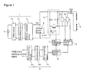
- Fig. 1 is a circuit diagram showing a first embodiment of the present invention.
- An input DC power source 1 includes a filter circuit 1a, a rectifying circuit 1b and a step-up chopper circuit 1c, rectifies and smoothes a commercial AC power source Vs and outputs a substantially constant input DC voltage Vdc.
- a control power circuit 2 is formed of, for example, a step-down chopper circuit using an IPD element (Refer to Fig. 4 described below), lowers the input DC voltage Vdc and generates a control power voltage Vcc.
- the DC-DC converter 3 is a step-down chopper circuit (back converter) including a switching element Q1, an inductor L1, a regenerative diode D1 and a smoothing capacitor C1, and the switching element Q1 is turned on/off at a high frequency, thereby converting the input DC voltage Vdc and outputting the converted voltage.
- back converter back converter
- a configuration of the step-down chopper circuit is known.
- a series circuit formed of the smoothing capacitor C1, the inductor L1 and the switching element Q1 is connected to the input DC power source 1, and the regenerative diode D 1 is connected to the series circuit formed of the smoothing capacitor C1 and the inductor L1 in parallel to constitute a closed circuit.
- An operation of turning on the switching element Q1 before completion of release of the energy in the inductor L1 is referred to as a continuous mode
- an operation of turning on the switching element Q1 at timing of completion of release of the energy in the inductor L1 is referred to as a critical mode
- an operation of turning on the switching element Q1 after completion of release of the energy in the inductor L1 through a suspension period is referred to as a discontinuous mode.
- the discontinuous mode is adopted, and in Patent literature 1, the continuous mode is adopted (Refer to Fig. 12 in Patent literature 1).
- An output of the DC-DC converter 3 is supplied to the semiconductor light-emitting element 4 via a connector CN2.
- the semiconductor light-emitting element 4 is, for example, a series circuit formed of LEDs, and its load voltage is detected by a voltage detecting circuit 5a and its load current is detected by a current detecting circuit 5b.
- a detection signal of each of the detecting circuits 5a, 5b is fed back to a feedback control circuit 6 and is used to control the switching element Q1.
- One or both of the detection circuits 5a, 5b may be used.
- the switching element Q1 is turned on/off at high frequency according to an output of a high-frequency oscillating circuit 7.
- a ratio of an ON time and an OFF time of the switching element Q1 by the high-frequency oscillating circuit 7 is set so that the DC-DC converter operates in the discontinuous mode in which energy stored from the input DC power source 1 into the inductor L1 in the ON period of the switching element Q1 is released through the regenerative diode D1 in the OFF period of the switching element Q1, and the switching element Q1 is turned on after completion of release of the energy in the inductor L1.
- the ratio of the switching element Q1 ON time/OFF time
- lighting can be stably achieved with a very minute optical output.
- the feedback control circuit 6 in the high luminance to medium luminance range having a relatively large heating value of the semiconductor light-emitting element 4, the feedback control circuit 6 is enabled, and an ON time width of the switching element Q1 by the high-frequency oscillating circuit 7 is feedback controlled according to an output of the feedback control circuit 6.
- the ratio ON time/OFF time
- the ratio can be set to be extremely small and therefore, dimmed lighting with a very minute optical output can be achieved.
- the dimming control circuit 8 feedback controls the ON time width of the switching element Q1 according to the high-frequency oscillating circuit 7 so that, in the high luminance to medium luminance range, the detection signal of each of the detecting circuits 5a, 5b converges to a target value according to a dimming control voltage from a dimming control signal circuit 9.
- the ON time width of the switching element Q1 by the high-frequency oscillating circuit 7 is fixed, or can be varied according to the dimming control voltage from the dimming control signal circuit 9 and the ratio of intermittent stopping of the high-frequency ON/OFF operation of the switching element Q1 can be varied according to the dimming control voltage from the dimming control signal circuit 9.
- the dimming control signal circuit 9 includes a nonpolarizing circuit 9a, an isolating circuit 9b and a DC converting circuit 9c, converts a dimming control signal received from the outside via a dimming control signal line and outputs a dimming control voltage.
- the dimming control signal received from the outside is, for example, a PWM signal having an amplitude of 10V and a frequency of about 1 kHz.
- the nonpolarizing circuit 9a is formed of, for example, a full-wave rectifier and nonpolarizes connecting polarity of the dimming control signal line.
- the isolating circuit 9b is formed of, for example, a photocoupler and isolates the dimming control signal line from the lighting device.
- the DC converting circuit 9c is formed of, for example, a smoothing circuit and outputs a DC voltage having a level corresponding to a pulse width of the PWM signal that is the dimming control signal, as the dimming control voltage.
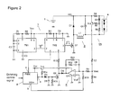
- FIG. 1 An embodiment further embodying a basic configuration shown in Fig. 1 will be described with reference to Fig. 2 .
- Fig. 2 is a circuit diagram of a second embodiment of the present invention.
- a configuration of the current detecting circuit 5b, the feedback control circuit 6 and the high-frequency oscillating circuit 7 in Fig. 1 is further embodied.
- the high-frequency oscillating circuit 7 is configured of general timer circuits TM1, TM2 and their peripheral circuits.
- the first timer circuit TM1 is an astable multivibrator for setting the ON/OFF frequency of the switching element Q1
- a second timer circuit TM2 is a monostable multivibrator for setting an ON pulse width of the switching element Q1.
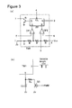
- the timer circuits TM1, TM2 each are a publicly known timer IC having an internal configuration shown in Fig. 3(a) (so-called 555), and is, for example, ⁇ PD5555 manufactured by Renesas Electronics Corporation (falling under old NEC Electronics Corporation) or its dual version ( ⁇ PD5556) or their compatibles.
- a 1st pin is a ground terminal and an 8th pin is a power terminal.
- a 2nd pin is a trigger terminal, and when a voltage at this terminal is lower than a half of a terminal at a 5th pin (generally, one third of the power voltage Vcc), an internal flip flop FF is set according to an output of a first comparator CP1, a 3rd pin (output terminal) becomes a High level and a 7th pin (discharging terminal) is put into an opened state.
- a 4th pin is a reset terminal, and when this terminal becomes a Low level, this terminal is put into an operation stopping state and the 3rd pin (output terminal) is fixed to a Low level.
- the 5th pin is a control terminal and a reference voltage as two thirds of the power voltage Vcc is generally applied to this terminal by an internal breeder resistor (series circuit formed of three resistors R).
- a 6th pin is a threshold terminal, and when a voltage at this terminal is higher than the voltage at the 5th pin (generally, two thirds of the power voltage Vcc), the internal flip flop FF is reset according to an output of a second comparator CP2, the 3rd pin (output terminal) becomes a Low level and the 7th pin (discharging terminal) is short-circuited to the 1st pin by an internal transistor Tr.
- the first timer circuit TM1 externally attaches time constant setting resistors R1, R2 and a capacitor C2 thereto and operates as the astable multivibrator.
- a voltage of the capacitor C2 is inputted to the 2nd pin (trigger terminal) and the 6th pin (threshold terminal) and is compared with the internal reference voltage (one third, two thirds of the power voltage Vcc).
- the voltage of the 5th pin is stabilized by a capacitor C3.
- the capacitor C2 When the voltage of the capacitor C2 is higher than the reference voltage (two thirds of the power voltage Vcc) compared at the 6th pin (threshold terminal), the 3rd pin (output terminal) becomes a Low level and the 7th pin (discharging terminal) is short-circuited to the 1st pin. Thereby, the capacitor C2 is discharged via the resistor R1.
- the 3rd pin When the voltage of the capacitor C2 is lower than the reference voltage (one third of the power voltage Vcc) compared at the 2nd pin (trigger terminal), the 3rd pin (output terminal) becomes a High level and the 7th pin (discharging terminal) is put into the opened state. Thereby, the capacitor C2 is charged from the power voltage Vcc via the resistors R2, R1 again. Thereafter, the same operations are repeated.
- the time constants of the resistors R1, R2 and the capacitor C2 are set so that an oscillating frequency of the 3rd pin (output terminal) becomes a high frequency of a few dozens of kHz.
- Resistance values of the resistors R1, R2 are set so that the resistance value of R1 is extremely smaller than the resistance value of R2. For this reason, a period during which the capacitor C2 is discharged via the resistor R1 (a period during which the output terminal of the 3rd pin is at a Low level) becomes extremely smaller than a period during which the capacitor C2 is charged via the resistors R2, R1 (a period during which the output terminal of the 3rd pin is at a High level).
- a pulse of Low level having a short pulse width is repeatedly outputted from the 3rd pin (output terminal) of the first timer circuit TM1 at a high frequency of a few dozens of kHz.
- the 2nd pin of the second timer circuit TM2 is triggered once every one cycle.
- the second timer circuit TM2 externally attaches a time constant setting resistor R3 and a capacitor C4 thereto, and operates as a monostable multivibrator.
- a pulse of Low level having a short pulse width is inputted to a 2nd pin (trigger terminal) of the second timer circuit TM2
- a 3rd pin (output terminal) of the second timer circuit TM2 becomes a High level and a 7th pin (discharging terminal) is put into the opened state.
- the capacitor C4 is charged via the time constant setting resistor R3.
- the capacitor C4 is instantaneously discharged.
- a pulse width of a pulse signal of a High level is determined depending on time required to charge the capacitor C4 from a ground voltage to the reference voltage (voltage at the 5th pin).
- a maximum value of the time is set to be shorter than an oscillating cycle of the first timer circuit TM1.
- a minimum value of the time is set to be longer than a pulse width of a trigger pulse of a Low level, which is outputted from the 3rd pin of the first timer circuit TM1.
- the pulse signal of a High level which is outputted from the 3rd pin of the second timer circuit TM2, becomes an ON driving signal of the switching element Q1.
- the ON time width can be controlled by the voltage at the 5th pin of the second timer circuit TM2, and becomes smaller as the voltage at the 5th pin is lower.
- the feedback control circuit 6 is configured of an operational amplifier OP1 and its peripheral circuit.
- a feedback impedance formed of resistors R11, R12 and a capacitor C6 is connected between an inverting input terminal and an output terminal of the operational amplifier OP1.
- a reference voltage Vref is applied to a non-inverting input terminal of the operational amplifier OP1.
- a voltage of the output terminal of the operational amplifier OP1 varies so that a voltage of the inverting input terminal of the operational amplifier OP1 corresponds to the voltage of the non-inverting input terminal (reference voltage Vref).
- a detection voltage Vdet of the current detecting circuit 5b is inputted to the inverting input terminal of the operational amplifier OP1 via a first input resistor R9, and a dimming control voltage Vdim is inputted from the dimming control circuit 8 to the inverting input terminal of the operational amplifier OP1 via a second input resistor R10.
- the ON time width of the switching element Q1 decreases, and conversely, when the detection voltage Vdet decreases, the ON time width of the switching element Q1 increases. That is, feedback control is achieved so as to suppress variation in the output. In this manner, the ON time width of the switching element Q1 is controlled so that the detection voltage Vdet corresponds to a magnitude of the dimming control voltage Vdim.
- the above-mentioned operation is made in the high luminance to medium luminance range.
- the low luminance range for example, a low luminous flux range less than 10% of full lighting
- feedback control by the operational amplifier OP1 is stopped and the ON time width of the switching element Q1 is fixed to a minimum value and in place of this, the high frequency ON/OFF operation of the switching element Q1 is intermittently stopped, thereby performing further dimming control.
- a terminal a of the dimming control circuit 8 is set to a High level.
- an ON driving signal is inputted to a control electrode of a switching element Q2 via a diode D3, so that the switching element Q2 is put into an ON state.
- the reference voltage at the 5th pin of the second timer circuit TM2 is fixed to a minimum value determined by a voltage division ratio of the internal breeder resistor and the resistor R13, and the ON time width of the switching element Q1 is fixed to a minimum value in a range that can be controlled by the operational amplifier OP1.
- the output voltage of the operational amplifier OP1 at the time when the terminal a of the dimming control circuit 8 is switched to a High level has the minimum value, that is, an anode potential of the diode D4 hardly varies before and after turning-on of the switching element Q2.
- the terminal a of the dimming control circuit 8 is switched to a Low level. Then, since the base current flows to the transistor Tr4 via the resistor R14, the transistor Tr4 is put into an ON state, thereby supplying the control power voltage Vcc to the operational amplifier OP1. Further, since the ON driving signal supplied via the diode D3 is blocked, the switching element Q2 is turned off. However, it is desired that the switching element Q2 remains to be in an ON state for a while until the operation of the operational amplifier OP1 becomes sufficiently stable.
- a timer circuit formed of a capacitor C5 and a resistor R15 is connected to the control electrode of the switching element Q2, and the time constant is set to about a time taken until the operation of the operational amplifier OP becomes sufficiently stable.
- the switching element Q2 gradually shifts to an OFF state.
- the operation of the operational amplifier OP1 becomes stable and a current via the resistor R13 is derived to the output terminal of the operational amplifier OP via the diode D4.
- the ON time width of the switching element Q1 is controlled by the operational amplifier OP1.
- the dimming control circuit 8 fixes the switching element Q2 to its ON state and the ON time width of the switching element Q1 is fixed to the minimum value. To further dimming control, it is need to extend the OFF time of the switching element Q1.
- the high frequency ON/OFF operation of the switching element Q1 is intermittently stopped.
- the terminal c In the high luminance to medium luminance range, the terminal c is fixed to a High level and the second timer circuit TM2 is operable at all times.
- the terminal c In the low luminance range, the terminal c is switched to High/Low at a low frequency, and a ratio of the period of Low level is controlled to be longer as dimming becomes deeper (luminance becomes lower).
- the ratio (ON time/OFF time) can be controlled to an extremely small value and therefore, dimmed lighting can be achieved with a very minute optical output.
- a bypass circuit for passing a bypass current larger than a lighting current is provided in parallel with the semiconductor light-emitting element 4 (Refer to Unexamined Patent Publication No. 2011-65922 ).
- a detection range of the current detecting circuit 5b is extended by efficiently utilizing such a bypass circuit.
- a series circuit formed of a diode D2 and a resistor R6 is connected in parallel with the semiconductor light-emitting element 4.
- the resistor R6 may be replaced with a constant current circuit.
- the diode D2 has the almost same temperature characteristics as a diode between a base and an emitter of a transistor Tr3. Since a forward voltage of the diode D2 and the voltage between the base and the emitter of the transistor Tr3 substantially offset each other, a voltage between both ends of a current detecting resistor R4 can be copied as a voltage between both ends of a base bias resistor R5.
- the current detecting resistor R4 has a low resistance and the base bias resistor R5 has a high resistance, a current flowing to the base bias resistor R5 is obtained by dividing the voltage between both ends by the resistor R5, and therefore, the base current corresponding to the current flowing to the current detecting resistor R4 (lighting current + bypass current) can be passed to the transistor Tr3. Since a collector current corresponding to the base current flows to a series circuit formed of resistors R7, R8, the detection voltage Vdet corresponding to the voltage between both ends of a current detecting resistor R4 can be obtained between both ends of the resistor R8.
- the bypass circuit constituted of the series circuit formed of the diode D2 and the resistor R6 does not exist, the voltage between both ends of the current detecting resistor R4 as low resistance becomes weaker as the lighting current lowers, the diode between the base and the emitter of the transistor Tr3 is not turned on, making current detection difficult.
- the voltage between both ends of the current detecting resistor R4 can be increased even when the lighting current is small.
- the diode between the base and the emitter of the transistor Tr3 can be turned on by a forward voltage of the diode D2, even when a load current is small, the lighting current can be detected.
- the current detecting resistor R4 should detect only the lighting current flowing to the semiconductor light-emitting element 4, in the present embodiment, the current detecting resistor R4 detects a current increased by the bypass current flowing to the series circuit formed of the diode D2 and the resistor R6 in addition to the lighting current flowing to the semiconductor light-emitting element 4.
- a load voltage of the semiconductor light-emitting element 4 is relatively stable, a varying range of the bypass current is smaller than that of the lighting current.
- an effect of the bypass current can be easily removed, for example, by replacing the resistor R6 with a constant current circuit, the lighting current can be detected in practice.
- the detection voltage Vdet mainly reflects the lighting current and increase of the bypass current can be ignored.
- the dimming control circuit 8 in Fig. 2 may be configured of a microcomputer.
- an analog dimming control voltage outputted from the dimming control signal circuit 9 in Fig. 1 is read from an A/D conversion input port, the dimming control voltage Vdim is determined by referring an internal memory table on the basis of the read value and the determined dimming control voltage Vdim is outputted from a D/A conversion output terminal b.
- the terminal a is set to a Low level and the terminal c is fixed to a High level.
- the terminal a In the low luminance range, to stop feedback control, the terminal a is set to a High level, and to intermittently stop the high frequency ON/OFF operation at a low frequency, the terminal c is switched to High/Low at a low frequency.
- a ratio of a Low level period may be determined referring to an internal memory table on the basis of the value of the analog dimming control voltage outputted from the dimming control signal circuit 9 in Fig. 1 , which is read from the A/D conversion input port.
- Fig. 3(b) shows a configuration of a main part according to a third embodiment of the present invention.
- the frequency of a high frequency ON/OFF operation of the switching element Q1 is made variable.
- the frequency of the high frequency ON/OFF operation of the switching element Q1 is lower as it approaches to a dimming control lower limit.
- a voltage at the 5th pin of the first timer circuit TM1 is determined based on a voltage division ratio of an internal breeder resistor (refer to Fig. 3(a) ) and the external resistor Ro and is lower than two thirds of Vcc. For this reason, an oscillating frequency of the first timer circuit TM1 is higher as compared to a case where the voltage at the 5th pin is two thirds of Vcc.
- the switching element Q3 is intermittently turned off.
- the voltage at the 5th pin of the first timer circuit TM1 rises toward two thirds of Vcc. For this reason, the high frequency oscillating frequency of the first timer circuit TM1 lowers.
- the number of times the switching element Q1 is turned on decreases, dimmed lighting can be achieved with a very minute optical output.
- Fig. 4 is a circuit diagram of a fourth embodiment of the present invention.
- the switching element Q1 of a step-down chopper circuit is arranged on a high potential side and the semiconductor light-emitting element 4 is arranged on a low potential side. Since the semiconductor light-emitting element 4 is arranged on the low potential side, the lighting current flowing to the semiconductor light-emitting element 4 can be detected more easily as compared to other embodiments.
- the feedback control circuit 6 is arranged on the low potential side, so that a control target signal acquired from a dimming control circuit 80 can be directly compared with a detection signal acquired from the current detecting resistor R4.
- the switching element Q1 since the switching element Q1 is arranged on a high potential side, any driving circuit needs to be arranged on the high potential side.
- the high-frequency oscillating circuit 7 formed of the timer circuits TM1 and TM2 is arranged on the high potential side.
- a configuration of the high-frequency oscillating circuit 7 in the present embodiment is basically the same as the high-frequency oscillating circuit 7 in the second embodiment in Fig. 2 , photocouplers PC1, PC2 are added to the timer circuit TM2 in a second stage in the present embodiment.
- a reference voltage at the 5th pin is variably controlled and the time constant setting resistor R3 is set to a fixed value.
- the reference voltage at the 5th pin is set to a fixed value stabilized by a capacitor C8, and a series circuit formed of a resistor R17 and a light receiving element of the photocoupler PC1 is connected in parallel with the time constant setting resistor R3.
- a current amount of a light emitting element of the photocoupler PC1 is controlled by the feedback control circuit 6.
- a light receiving element of the photocoupler PC2 that can be turned on/off at low frequency is inserted between the 8th pin and the 4th pin of the timer circuit TM2, and the 4th pin is pulled down to a potential at the 1st pin by a resistor R18.
- Alight emitting element of the photocoupler PC2 can be switched between conduction/blocking at a low frequency by the dimming control circuit 80. When the current flows to the light emitting element of the photocoupler PC2, the light receiving element of the photocoupler PC2 is turned on. When the current flowing to the light emitting element of the photocoupler PC2 is blocked, the light receiving element of the photocoupler PC2 is turned off.
- the timer TM2 becomes operable and operates as the monostable multivibrator.
- the high-frequency oscillating circuit 7 When the high-frequency oscillating circuit 7 is arranged on the high potential side as in the present embodiment, as distinct from the case where the high-frequency oscillating circuit 7 is arranged on the low potential side, it is no need to transmit a high frequency control signal from the low potential side to the high potential side. That is, since a transmission signal of the photocoupler PC1 in Fig. 4 is an analog signal relating to control of an ON time width of the switching element Q1 and a transmission signal of the photocoupler PC2 is a low frequency ON/OFF signal for burst dimming control, both the photocouplers can use an inexpensive element having a low transmission rate.
- the high-frequency oscillating circuit 7 is arranged on the low potential side, a driving ability of the timer circuit TM2 in the second stage cannot be directly applied to ON/OFF control of the switching element Q1 on the high potential side and furthermore, it is need to transmit the control signal to a driving circuit separately provided on the high potential side by use of a high-speed photocoupler. Therefore, as shown in Fig. 4 , it is advantageous that the high-frequency oscillating circuit 7 formed of the timer circuits TM1, TM2 is arranged on the high potential side.
- control power circuit 2 that can supply the control power voltages Vcc, HVcc to the low potential side and the high potential side irrespective of the dimmed lighting state is connected in parallel with the semiconductor light-emitting element 4.
- the control power circuit 2 needs to flow a necessary consumption current at all times to generate the stable control power voltages Vcc, HVcc, dimmed lighting of the semiconductor light-emitting element 4 is stabilized by effectively using the current as the bypass current.
- a configuration of the control power circuit 2 will be described below.
- the control power circuit 2 formed of an IPD element IC1 and its peripheral circuit is connected to the smoothing capacitor C1 to which the semiconductor light-emitting element 4 is connected.
- the IPD element IC1 is a so-called intelligent power device such as MIP2E2D manufactured by Panasonic Corporation. This element is a three-pin IC having a drain terminal D, a source terminal S and a control terminal C, and includes a switching element as a power MOSFET and a control circuit for controlling its ON/OFF operation therein.
- the switching element included between the drain terminal D and the source terminal S of the IPD element IC1, an inductor L2, a smoothing capacitor C13 and a diode D7 constitute a step-down chopper circuit.
- a Zener diode ZD3, a diode D8, a smoothing capacitor C12 and a capacitor C11 constitute a power circuit of the IPD element IC1.
- a voltage of the smoothing capacitor C1 rises via an activating circuit 21
- a current flows in a path of the drain terminal D and the control terminal C of the IPD element IC1, the smoothing capacitor C 12, the inductor L2 and the smoothing capacitor C 13 in this order, thereby charging the smoothing capacitor C 12 to illustrated polarity.
- the voltage of the smoothing capacitor C12 becomes an operating power for a control circuit in the IPD element IC1, the IPD element IC1 starts its operation and a switching element between the drain terminal D and the source terminal S starts to be turned on/off.
- the control circuit in the IPD element IC1 controls turning-on/off of the switching element between the drain terminal D and the source terminal S of the IPD element IC1 so that the voltage Vc12 of the capacitor C12 connected between the source terminal S and the control terminal C becomes constant. This makes the voltage of the smoothing capacitor C13 constant and at the same time, provides an operating power to the IPD element IC1.
- the smoothing capacitor C 13 acquires the control power voltage Vcc
- the dimming control circuit 80 and the feedback control circuit 6 start their operations, and the control power voltage HVcc is supplied to timer circuits IC1, IC2 arranged on the high potential side from a high-side power circuit.
- the high-side power circuit charges a smoothing capacitor C9 via a diode D5 and a resistor R19 with an output of a secondary winding L2a of the inductor L2 of the control power circuit 2 arranged on the low potential side, and the charging voltage HVcc is made constant by a zener diode ZD1.
- the timer circuits TM1, TM2 start their operations, thereby turning on/off the switching element Q1 at a high frequency.
- the activating circuit 21 of the control power circuit 2 will be described.
- a current flows to the smoothing capacitor C1 via a resistor R20, a part between a base and an emitter of a transistor Tr5 and a resistor R22, thereby turning on the transistor Tr5 and charging the smoothing capacitor C1 via a resistor R21, a part between a collector and the emitter of the transistor Tr5 and the resistor R22.
- the charging voltage of the smoothing capacitor C1 reaches an activating voltage for the IPD element IC1 of the control power circuit 2, the IPD element IC1 starts its oscillating operation.
- the smoothing capacitor C 13 acquires the control power voltage Vcc on the low potential side
- the smoothing capacitor C9 for a power source for the timer circuits TM1, TM2 acquires the control power voltage HVcc on the high potential side.
- the ON/OFF operation of the switching element Q1 is started, and the charging voltage of the smoothing capacitor C1 further rises.
- a zener voltage of a zener diode ZD2 is set to be higher than the activating voltage for the IPD element IC1 of the control power circuit 2, and to be lower than a light-emitting voltage for the semiconductor light-emitting element 4 (for example, 80V to 98V). For this reason, when the switching element Q1 starts the ON/OFF operation and the voltage of the smoothing capacitor C1 reaches the light-emitting voltage for the semiconductor light-emitting element 4, a current flows in a path of the smoothing capacitor C1, the resistor R22, a diode D6 and the zener diode ZD2 in the reverse direction, thereby reverse biasing the part between the base and the emitter of the transistor Tr5. As a result, a part between the collector and the emitter of the transistor Tr5 is kept in its OFF state and an activating current via the transistor Tr5 is blocked.
- a sum of a consumption current of the control power circuit 2 and a consumption current via a series circuit formed of the resistor R22 and the diode D6 of the activating circuit 21 and the zener diode ZD2 is set to be equal to or larger than the bypass current (for example, 6 to 7mA) flowing through the diode D2 and the resistor R6 in the second embodiment.
- the bypass current for example, 6 to 7mA
- the feedback control circuit 6 is constituted of an feedback control integrated circuit IC3 (for example, NJM2146B manufactured by New Japan Radio Co., Ltd.) that has operational amplifiers A1, A2 and an output transistor Q4 therein, and its peripheral circuit.
- the detection voltage of the current detecting resistor R4 is inputted to a + input terminal (3rd pin) of the operational amplifier A1 via an input resistor R61, and a control target voltage outputted from the dimming control circuit 80 is inputted to a - input terminal (2nd pin).
- a series circuit formed of a resistor R62 and the capacitor C62, which are connected between the output terminal (1st pin) and the + input terminal (3rd pin), is a feedback impedance.
- the other operational amplifier A2 is not used in the present embodiment, it may be used for voltage feedback control to stabilize an applied voltage of the semiconductor light-emitting element 4 to a target voltage when dimmed lighting is deep, as needed (see JPA 2009-232623).
- the control power voltage Vcc is supplied between a power terminal (8th pin) and a ground terminal (4th pin) of the integrated circuit IC3 from the smoothing capacitor C13.
- the light emitting element of the photocoupler PC1 is connected between the power terminal (8th pin) and an output terminal (1st pin) of the integrated circuit IC3 via a resistor R63.
- a resistance value of the transistor Q4 decreases and a current flowing to the light emitting element of the photocoupler PC1 increases, and thus, a resistance value of the light receiving element of the photocoupler PC 1 lowers.
- the ON time width of the switching element Q1 is controlled to be shortened, the voltage of the smoothing capacitor C1 lowers and the lighting current detected by the current detecting resistor R4 decreases.
- the resistance value of the transistor Q4 increases and the current flowing to the light emitting element of the photocoupler PC 1 decreases and thus, the resistance value of the light receiving element of the photocoupler PC1 increases.
- the ON time width of the switching element Q1 is controlled to be extended, the voltage of the smoothing capacitor C1 rises and the lighting current detected by the current detecting resistor R4 increases.
- the lighting current detected by the current detecting resistor R4 is controlled to be a constant value corresponding to the target current set by the dimming control circuit 80.
- feedback control may be stopped by stopping power supply to the 8th pin of the integrated circuit IC3 and short-circuiting the 1st pin to a ground level.
- the dimming control circuit 80 is configured of a photocoupler PC3 for receiving a dimming control signal as a low frequency PWM signal, a Schmidt inverter IC2 for shaping a waveform of the received optical output and their peripheral circuits.
- the Schmidt inverter IC2 is, for example, TC7SH14F manufactured by TOSHIBA CORPORATION.
- an input voltage is higher than an upper threshold value, an output voltage becomes a Low level, and when the input voltage is lower than a lower threshold value, the output voltage becomes a High level.
- the output voltage has a hysteresis characteristic of about 20 to 30% of the power voltage Vcc between the upper threshold value and the lower threshold value, and even when a waveform of the input voltage remains, the output voltage becomes a rectangular wave voltage, the waveform of which is shaped.
- An input terminal of the Schmidt inverter IC2 is connected to a line of the control power voltage Vcc via a pull-up resistor R85, and also is connected to the ground via a series circuit formed of a resistor R84 and a transistor Q5.
- the capacitor C82 connected to the series circuit formed of the resistor R84 and the transistor Q5 in parallel is a small-capacity noise removing capacitor and has no smoothing function.
- a bias voltage obtained by dividing the control power voltage Vcc by a resistance voltage dividing circuit formed of resistors R82, R83 is supplied between a base and an emitter of the transistor Q5.
- a capacitor C81 is connected to the resistor R83 in parallel, and the light receiving element of the photocoupler PC3 is connected to the resistor R83 via a resistor R81 in parallel.
- the capacitor C81 is a small-capacity noise removing capacitor and has no smoothing function.
- the dimming control signal as a low frequency PWM signal (for example, a rectangular wave voltage signal of 1 kHz, 10V) is inputted to the light emitting element of the photocoupler PC3 via a resistor (not shown).
- This type of dimming control signal is widely used in the field of an inverter lighting device of a fluorescent lamp.
- the dimming control signal When the dimming control signal is at a High level, the light receiving element of the photocoupler PC3 is turned on according to an optical signal of the light emitting element of the photocoupler PC3, and a base bias of the transistor Q5 is biased, resulting in that the transistor Q5 is in a high resistance state.
- the input voltage of the Schmidt inverter IC2 becomes higher than the upper threshold value, the output voltage of the Schmidt inverter IC2 becomes a Low level.
- the dimming control signal When the dimming control signal is at a Low level, the optical signal of the light emitting element of the photocoupler PC3 disappears. As a result, since the light receiving element of the photocoupler PC3 is turned off and a base bias is supplied to the transistor Q5 via the resistor R82, the transistor Q5 is in a low resistance state. Thus, when the input voltage of the Schmidt inverter IC2 becomes lower than the lower threshold value, the output voltage of the Schmidt inverter IC2 becomes a High level.
- the capacitor C83 When the output voltage of the Schmidt inverter IC2 is at a High level, the capacitor C83 is charged via a diode D9 and a resistor R87, and a voltage of the capacitor C83 rises. A discharging resistor R88 is connected to the capacitor C83 in parallel. When the output voltage of the Schmidt inverter IC2 is at a Low level, the voltage of the capacitor C83 lowers.
- the time constant for charging/discharging is set to be comparatively larger than a cycle of the dimming control signal, and the capacitor C83 has a substantial smoothing function.
- the voltage of the capacitor C83 is a voltage corresponding to a period during which the output voltage of the Schmidt inverter IC2 is at a High level, and becomes higher as a period during which the dimming control signal inputted to the photocoupler PC3 is at a Low level becomes longer.
- the light emitting element of the photocoupler PC2 is connected to the output of the Schmidt inverter IC2 via a resistor R86.
- a current flows to the light emitting element of the photocoupler PC2 via the resistor R86.
- the timer circuit TM2 becomes operable.
- the output voltage of the Schmidt inverter IC2 is at a Low level, since no current flows to the light emitting element of the photocoupler PC2, the light receiving element of the photocoupler PC2 is turned off.
- timer circuit TM2 becomes inoperable.
- the output voltage of the Schmidt inverter IC2 is at a High level, that is, the low frequency PWM signal received by the photocoupler PC3 of the dimming control circuit 80 is at a Low level
- the high frequency ON/OFF operation of the switching element Q1 is allowed
- the output voltage of the Schmidt inverter IC2 is at a Low level, that is, the low frequency PWM signal received by the photocoupler PC3 of the dimming control circuit 80 is at a High level
- the switching element Q1 is kept in its OFF state. In this manner, burst dimming control is performed according to the low frequency PWM signal received by the photocoupler PC3.
- the ON pulse width of the switching element Q1 is feedback controlled by the feedback control circuit 6. That is, the ON pulse width of the switching element Q1 is controlled so that a detected value of the smoothed DC current flowing from the smoothing capacitor C1 to the semiconductor light-emitting element 4, which is detected by the current detecting resistor R4, matches the voltage of the capacitor C83 of the dimming control circuit 80.
- a capacitor C10 is a small-capacity film capacitor for bypassing high-frequency ripple of the smoothing capacitor C1.
- a capacitor C7 as an input DC power source is an output capacitor of the step-up chopper circuit 1c as shown in Fig. 1 , and the voltage Vdc is controlled to be constant.
- the control power voltage Vcc generated by the control power circuit 2 may be supplied to a PFC control circuit for controlling a step-up chopper circuit.
- Fig. 5 is a circuit diagram of a fifth embodiment of the present invention.
- the high-frequency oscillating circuit 7 is configured of a single timer circuit TM.
- a PWM control circuit IC4 performs control to intermittently stop the high frequency oscillating operation at a low frequency and control of the high frequency ON time width and OFF time width.
- the PWM control circuit IC4 sets a 4th pin of the timer circuit TM to a High level.
- the general timer IC (so-called 555) shown in Fig. 3(a) can be used as the timer circuit TM.
- the timer circuit TM operates as an astable multivibrator. When a voltage at a 2nd pin is lower than a half of a voltage at a 5th pin, an internal flip flop is inverted and a 3rd pin becomes a High level and a 7th pin is opened, so that the capacitor C4 is charged via a charging resistor Rc and a diode D10.
- the internal flip flop When the charging voltage of the capacitor C4, which is applied to a 6th pin, is higher than the voltage at the 5th pin, the internal flip flop is inverted and the 3rd pin (output terminal) becomes a Low level, so that the 7th pin (discharging terminal) is short-circuited to the 1st pin. As a result, the capacitor C4 is discharged via a discharging resistor Rd and its voltage lowers.
- the charging voltage of the capacitor C4, which is applied to the 2nd pin is lower than a half of the voltage at the 5th pin, the internal flip flop is inverted, the 3rd pin becomes a High level and the 7th pin is opened, so that the capacitor C4 is charged via the charging resistor Rc and the diode D10. Thereafter, the same operations are repeated.
- the timer circuit TM operates as the general astable multivibrator
- the ON time width of the switching element Q1 is a variable width determined according to the time constants of the charging resistor Rc and the capacitor C4, and the voltage at the 5th pin.
- An OFF time width of the switching element Q1 is a variable width determined according to the time constants of the discharging resistor Rd and the capacitor C4, and the voltage at the 5th pin. Accordingly, the switching element Q1 is driven with the ON time width and the OFF time width that correspond to the voltage at the 5th pin of the timer circuit TM.
- a ratio of the ON time width and the OFF time width so that when the voltage at the 5th pin is maximum, as shown in Fig. 6(a) , a current flows to the inductor L1 in a discontinuous mode close to a critical mode, even when the voltage at the 5th pin varies, the discontinuous mode can be made at all times.
- values of the resistors Rc, Rd and the capacitor C4 may be designed so that the ON time width is slightly smaller than that under a critical condition: "ON time width ⁇ (power voltage - load voltage) is almost equal to OFF time width ⁇ load voltage".
- a peak of the current flowing to the inductor L1 can be reduced and a suspension period of the current can be increased.
- an average current flowing to the inductor L1 in a burst ON period can be decreased.
- TL494 manufactured by Texas Instruments Incorporated or its equivalents can be used as the PWM control circuit IC4.
- This IC includes a sawtooth wave generator OSC, a comparator CP, error amplifiers EA1, EA2, output transistors Tr1, Tr2 and a reference voltage source therein, oscillates at a fixed frequency determined by a capacitor Ct and a resistor Rt that are externally added to the 5th pin and the 6th pin, respectively, and generates a PWM signal with a pulse width corresponding to a voltage at the 3rd pin.
- the oscillating frequency may be, for example, a low frequency such as 1 kHz.
- the 4th pin is a dead time setting terminal and is connected to the ground in the present embodiment.
- the error amplifier EA1 connected to the 1st and 2nd pins is diode OR connected to the error amplifier EA2 connected to 15th and 16th pins, and a larger output becomes a reference voltage of the comparator CP.
- the second error amplifier EA2 is not used.
- a 13rd pin is a terminal for selecting a single end operation and a push pull operation.
- the single end operation is selected by connection to the ground.
- operations of the transistors Tr1, Tr2 are the same as each other by internal logic circuits.
- the 4th pin of the timer circuit TM becomes a Low level, so that the high frequency oscillating operation of the high-frequency oscillating circuit 7 is stopped and the switching element Q1 is kept in its OFF state.
- the transistor Tr 2 is turned off, the 4th pin of the timer circuit TM is pulled up to a potential of the control power voltage Vcc by a resistor R33, and the high frequency oscillating operation of the high-frequency oscillating circuit 7 is started.
- the ON time width of the switching element Q1 together with the burst ON period of the switching element Q1 is also feedback controlled.
- a feedback control circuit is configured of the error amplifier EA1 and an external CR circuit.
- a feedback impedance formed of the resistors R11, R12 and the capacitor C6 is connected between an inverting input terminal and the output terminal of the error amplifier EA1.
- a constant voltage obtained by dividing a reference voltage Vref at the 14th pin by the resistors R31, R32 is applied to a non-inverting input terminal of the error amplifier EA1.
- the voltage of the output terminal of the error amplifier EA1 varies so that the voltage of the inverting input terminal of the error amplifier EA1 matches the voltage of the non-inverting input terminal.
- the inverting input terminal of the error amplifier EA1 receives a detection voltage Vdet of the output detecting circuit 5 via the first input resistor R9 and receives the dimming control voltage Vdim via the second input resistor R10.
- the dimming control voltage Vdim increases, the output voltage of the error amplifier EA1 lowers and the ON period of the transistors Tr1, Tr2 increases, resulting in that a period during which the ON/OFF operation of the switching element Q1 is stopped increases. Further, since a reference voltage at the 5th pin of the timer circuit TM lowers, the ON time width of the switching element Q1 decreases. Conversely, when the dimming control voltage Vdim decreases, the output voltage of the error amplifier EA1 rises and the ON period of the transistors Tr1, Tr2 decreases, resulting in that the period during which the ON/OFF operation of the switching element Q1 is stopped decreases. Further, since the reference voltage at a 5th pin of the timer circuit TM rises, the ON time width of the switching element Q1 increases.
- the semiconductor light-emitting element 4 is serially connected with the current detecting resistor R4 and is parallel connected with a bypass circuit as a series circuit formed of voltage dividing resistors R16, R6 and a zener diode ZD4.
- a constant of the bypass circuit is set so as to pass a bypass current larger than the lighting current flowing to the semiconductor light-emitting element 4 in the vicinity of the dimming control lower limit. Thereby, stable dimmed lighting can be achieved in the vicinity of the dimming control lower limit.
- the output detecting circuit 5 When a value of the resistor R4 is zero, the output detecting circuit 5 functions as the voltage detecting circuit 5a and when a value of the resistor R16 is zero, the output detecting circuit 5 functions as the current detecting circuit 5b. By properly setting the values of the resistors R4, R16, the output detecting circuit 5 functions as a circuit for detecting load power in a pseudo manner.
- a current corresponding to a sum of the lighting current flowing to the semiconductor light-emitting element 4 and the bypass current flowing to the bypass circuit flows to the resistor R4. Accordingly, even when the lighting current flowing to the semiconductor light-emitting element 4 is close to zero, a voltage by the bypass current flowing to the bypass circuit (increased voltage) occurs at the resistor R4, thereby preventing the transistor Tr3 from being blocked.
- a zener voltage of the zener diode ZD4 is set to be lower than a voltage that can light the semiconductor light-emitting element 4.
- the bypass current flowing to the bypass circuit is used as a bias current for conduction of the diode between the base and the emitter of the output detecting transistor Tr3.
- the output detecting transistor Tr3 is not blocked and can be biased so as to operate in an active range at all times.
- the lighting current and the applied voltage of the semiconductor light-emitting element 4 may be separately detected to perform feedback control according to the lighting current by the first error amplifier EA1 as well as to perform feedback control according to the applied voltage by the second error amplifier EA2. It is known that it is preferred to perform former control in the high luminance to medium luminance range and to perform latter control in the low luminance range (Refer to JPA 2009-232623)
- FIGs. 7(a) to 7(c) various switching power circuits as shown in FIGs. 7(a) to 7(c) may be used as the DC-DC converter according to the present invention.
- Fig. 7(a) shows a step-up chopper circuit 3a
- Fig. 7(b) shows a flyback converter circuit 3b
- Fig. 7(c) shows a step-up/down chopper circuit 3c.
- the DC-DC converter includes at least the switching element Q1, the inductive element (the inductor L1 or a transformer T1) and the regenerative diode D1, and operates in the discontinuous mode in which energy stored from the DC power source into the inductive element during the ON period of the switching element Q1 is released via the regenerative diode D1 during the OFF period of the switching element Q1, and after completion of release of the energy in the inductive element, the switching element Q1 is turned on.
- Fig. 8 shows a schematic configuration of a power source-separated type LED illumination fixture using the LED lighting device according to the present invention.
- the power source-separated type LED illumination fixture includes a lighting device 30 as a power source unit in a case other than a housing 42 of an LED module 40. This can make the LED module 40 thinner and the lighting device 30 as the separated-type power source unit can be installed at any place.
- the fixture housing 42 is formed of a metallic cylindrical body having an opened lower end, and the opened lower end is covered with a light diffusing plate 43.
- the LED module 40 is arranged as opposed to the light diffusing plate 43.
- An LED mounting board 41 mounts LEDs 4a, 4b, 4c, ... of the LED module 40 thereon.
- the fixture housing 42 is embedded in a ceiling 100, and is wired from the lighting device 30 as the power source unit arranged in the ceiling cavity via a lead 44 and a connector 45.
- the circuits described in each of the above-mentioned embodiments are stored in the lighting device 30 as the power source unit.
- the series circuit formed of the LEDs 4a, 4b, 4c, ... (LED module 40) corresponds to the semiconductor light-emitting element 4.
- the power source-separated type LED illumination fixture is exemplified, in which the lighting device 30 as the power source unit is stored in the housing other than the housing of the LED module 40.
- the lighting device according to the present invention may be applied to a power source-integrated type LED illumination fixture in which the power source unit and the LED module 40 are stored in the same housing.
- the lighting device according to the present invention is not limited to the illumination fixture and may be used as, for example, a backlight of a liquid crystal display, and a light source for a copier, a scanner, a projector and the like.
- the semiconductor light-emitting element 4 is not limited to this, and may be, for example, an organic EL element and a semiconductor laser element.
- the MOSFET is exemplified as the switching element Q1, other switching elements such as IGBT may be used.
Applications Claiming Priority (1)
| Application Number | Priority Date | Filing Date | Title |
|---|---|---|---|
| JP2011092474A JP5891454B2 (ja) | 2011-04-18 | 2011-04-18 | 半導体発光素子の点灯装置およびそれを用いた照明器具 |
Publications (3)
| Publication Number | Publication Date |
|---|---|
| EP2515614A2 true EP2515614A2 (de) | 2012-10-24 |
| EP2515614A3 EP2515614A3 (de) | 2013-11-06 |
| EP2515614B1 EP2515614B1 (de) | 2017-11-08 |
Family
ID=46045798
Family Applications (1)
| Application Number | Title | Priority Date | Filing Date |
|---|---|---|---|
| EP12164293.8A Not-in-force EP2515614B1 (de) | 2011-04-18 | 2012-04-16 | Beleuchtungsvorrichtung für ein lichtemittierendes Halbleiterelement und Beleuchtungsbefestigung damit |
Country Status (4)
| Country | Link |
|---|---|
| US (1) | US8680788B2 (de) |
| EP (1) | EP2515614B1 (de) |
| JP (1) | JP5891454B2 (de) |
| CN (1) | CN102752908A (de) |
Cited By (3)
| Publication number | Priority date | Publication date | Assignee | Title |
|---|---|---|---|---|
| WO2014153580A1 (de) * | 2013-03-25 | 2014-10-02 | Tridonic Gmbh & Co. Kg | Led-konverter mit verbessertem emi-verhalten |
| GB2514380A (en) * | 2013-05-22 | 2014-11-26 | Bernard Frederick Fellerman | LED driver circuit |
| EP3011805B1 (de) * | 2013-09-19 | 2018-07-11 | Philips Lighting Holding B.V. | Ansteuerung für lichtemittierende diode mit differentialspannungsversorgung |
Families Citing this family (58)
| Publication number | Priority date | Publication date | Assignee | Title |
|---|---|---|---|---|
| US8467209B2 (en) * | 2010-07-27 | 2013-06-18 | Stmicroelectronics S.R.L. | Control device of a switching power supply |
| US10439508B2 (en) | 2010-07-27 | 2019-10-08 | Stmicroelectronics S.R.L. | Control device of a switching power supply |
| DE102010054899B4 (de) * | 2010-12-17 | 2018-07-12 | Austriamicrosystems Ag | Regelkreisanordnung, Schaltungsanordnung und Verfahren zur Regelung einer mit einer Last gekoppelten Stromquelle |
| TWI465011B (zh) * | 2011-06-02 | 2014-12-11 | Richtek Technology Corp | Pwm電壓調節器的控制電路及方法 |
| WO2013046160A1 (en) * | 2011-09-30 | 2013-04-04 | Koninklijke Philips Electronics N.V. | Active capacitor circuit |
| JP5838346B2 (ja) * | 2011-10-24 | 2016-01-06 | パナソニックIpマネジメント株式会社 | 点灯装置および、これを用いた照明器具 |
| ITMI20120088A1 (it) | 2012-01-26 | 2013-07-27 | Dora Spa | Dispositivo di controllo per un alimentatore a commutazione. |
| ITMI20120089A1 (it) | 2012-01-26 | 2013-07-27 | Dora Spa | Dispositivo di controllo per un alimentatore a commutazione. |
| JP5988207B2 (ja) * | 2012-09-07 | 2016-09-07 | パナソニックIpマネジメント株式会社 | 固体発光素子駆動装置及び照明装置、照明器具 |
| US8810157B2 (en) * | 2012-10-18 | 2014-08-19 | Power Integrations, Inc. | Simplified current sense for buck LED driver |
| WO2014071415A1 (en) * | 2012-11-05 | 2014-05-08 | Osram Sylvania Inc. | Driver for solid state light sources |
| US8836242B2 (en) * | 2012-11-29 | 2014-09-16 | Shenzhen China Star Optoelectronics Technology, Co., Ltd. | LED voltage adjustment device and drive system thereof |
| JP2014130699A (ja) * | 2012-12-28 | 2014-07-10 | Panasonic Corp | 発光素子点灯装置、および照明器具 |
| JP6012487B2 (ja) * | 2013-01-23 | 2016-10-25 | 旭化成エレクトロニクス株式会社 | Led調光回路 |
| CN103093728A (zh) * | 2013-01-29 | 2013-05-08 | 深圳市华星光电技术有限公司 | 一种led背光驱动电路及液晶显示器 |
| WO2014121662A1 (zh) * | 2013-02-08 | 2014-08-14 | 东林科技股份有限公司 | 定功率电源供应装置及定功率输出的控制方法 |
| DE102013203732A1 (de) * | 2013-03-05 | 2014-09-11 | Osram Gmbh | Schaltungsanordnung und Verfahren zum Betreiben mindestens eines Leuchtmittels |
| US9955547B2 (en) | 2013-03-14 | 2018-04-24 | Lutron Electronics Co., Inc. | Charging an input capacitor of a load control device |
| US9113521B2 (en) * | 2013-05-29 | 2015-08-18 | Lutron Electronics Co., Inc. | Load control device for a light-emitting diode light source |
| KR102149861B1 (ko) * | 2013-06-04 | 2020-08-31 | 온세미컨덕터코리아 주식회사 | 전력 공급 장치 및 그 구동 방법 |
| CN103347183A (zh) * | 2013-06-28 | 2013-10-09 | 成都思迈科技发展有限责任公司 | 一种数字视频光发射机 |
| JP6153024B2 (ja) * | 2013-07-26 | 2017-06-28 | パナソニックIpマネジメント株式会社 | 発光素子点灯装置、発光モジュール、照明装置及び発光素子の点灯方法 |
| CN104640269A (zh) * | 2013-11-08 | 2015-05-20 | 苏州璨宇光学有限公司 | 光源装置 |
| CN103944379B (zh) * | 2013-11-30 | 2016-06-15 | 上海晶丰明源半导体有限公司 | 直流转换开关降压开关电源 |
| JP6292503B2 (ja) * | 2013-12-16 | 2018-03-14 | パナソニックIpマネジメント株式会社 | 電源装置及びled点灯装置 |
| US9554431B2 (en) * | 2014-01-06 | 2017-01-24 | Garrity Power Services Llc | LED driver |
| JP2015170534A (ja) | 2014-03-07 | 2015-09-28 | パナソニックIpマネジメント株式会社 | 点灯装置及び照明器具 |
| CN116347450A (zh) * | 2014-07-07 | 2023-06-27 | 安晟信医疗科技控股公司 | 考虑到至少一个条件的改进装置配对 |
| JP6396160B2 (ja) * | 2014-10-02 | 2018-09-26 | 株式会社小糸製作所 | 車両用灯具およびその点灯回路 |
| JP6516178B2 (ja) | 2014-10-20 | 2019-05-22 | パナソニックIpマネジメント株式会社 | 調光制御ユニット、照明システム、及び設備機器 |
| JP6501177B2 (ja) | 2014-12-25 | 2019-04-17 | パナソニックIpマネジメント株式会社 | 点灯装置、該点灯装置を用いた照明器具、並びに、前記照明器具を用いた照明システム |
| JP6410179B2 (ja) * | 2015-01-19 | 2018-10-24 | パナソニックIpマネジメント株式会社 | 点灯装置、照明器具および照明システム |
| US9705412B2 (en) | 2015-02-26 | 2017-07-11 | Stmicroelectronics S.R.L. | Pulsed feedback switching converter |
| TWI580307B (zh) * | 2015-04-30 | 2017-04-21 | 立錡科技股份有限公司 | 發光元件驅動電路及其中之控制電路與控制方法 |
| JP2017021938A (ja) | 2015-07-08 | 2017-01-26 | パナソニックIpマネジメント株式会社 | 調光制御ユニット、照明システム、及び設備機器 |
| DE112015006702T5 (de) * | 2015-07-15 | 2018-04-05 | Mitsubishi Electric Corporation | Steuerungsschaltung |
| JP6566354B2 (ja) | 2015-08-25 | 2019-08-28 | パナソニックIpマネジメント株式会社 | 調光制御装置、照明システム、及び設備機器 |
| CN106793359B (zh) * | 2015-11-19 | 2019-10-18 | 台达电子企业管理(上海)有限公司 | 调光驱动电路及其控制方法 |
| WO2017134824A1 (ja) * | 2016-02-05 | 2017-08-10 | 俊蔵 大島 | 電源装置 |
| CN107347222B (zh) | 2016-05-04 | 2019-02-12 | 台达电子企业管理(上海)有限公司 | 调光驱动电路及其控制方法 |
| JP6928834B2 (ja) | 2016-12-07 | 2021-09-01 | パナソニックIpマネジメント株式会社 | 点灯装置、照明器具、及び、点灯装置の制御方法 |
| US10582578B2 (en) * | 2017-02-06 | 2020-03-03 | Ideal Industries Lighting Llc | Solid state light fixtures having variable current dimming and related driver circuits and methods |
| US9775205B1 (en) * | 2017-02-20 | 2017-09-26 | Nxp B.V. | Discontinuous mode buck converter and method therefor |
| US11277898B2 (en) * | 2017-07-06 | 2022-03-15 | Signify Holding B.V. | Retrofit light emitting diode, LED, lighting device for connection to a ballast, wherein said LED lighting device is arranged to detect a dip in said mains voltage using a zero current detector |
| JP6900830B2 (ja) * | 2017-08-09 | 2021-07-07 | 岩崎電気株式会社 | Led点灯回路及びled照明装置 |
| JP7026898B2 (ja) * | 2017-11-30 | 2022-03-01 | 株式会社フジキン | インバータ回路、x線照射装置 |
| JP6979588B2 (ja) * | 2018-02-23 | 2021-12-15 | パナソニックIpマネジメント株式会社 | 照明光通信装置 |
| CN108811251B (zh) * | 2018-07-06 | 2023-10-13 | 赛尔富电子有限公司 | 具有预防漏电功能的灯具调光电路及调光灯具 |
| US10531532B1 (en) * | 2018-07-10 | 2020-01-07 | Eaton Intelligent Power Limited | Setting current error reduction for light-emitting diode driver circuits |
| US10714028B2 (en) | 2018-09-27 | 2020-07-14 | Apple Inc. | Methods and apparatus for controlling display backlight |
| US10877314B2 (en) | 2018-09-27 | 2020-12-29 | Apple Inc. | Methods and apparatus for controlling display backlight |
| US11159085B2 (en) * | 2018-12-10 | 2021-10-26 | Fuji Electric Co., Ltd. | Integrated circuit and switching circuit |
| CN109842302B (zh) * | 2019-02-15 | 2020-08-14 | 矽力杰半导体技术(杭州)有限公司 | 串联谐振变换器及其原边反馈控制电路和控制方法 |
| JP7455572B2 (ja) * | 2019-12-23 | 2024-03-26 | 住友重機械工業株式会社 | 電源装置及びレーザ装置 |
| CN115211015A (zh) * | 2020-02-27 | 2022-10-18 | 罗姆股份有限公司 | 电源控制装置、dc-dc转换器及ac-dc转换器 |
| CN117652087A (zh) | 2021-07-14 | 2024-03-05 | 昕诺飞控股有限公司 | 开关模式功率转换器 |
| CN115413082A (zh) * | 2022-08-08 | 2022-11-29 | 重庆绿色科技开发(集团)有限公司 | 物联网红绿蓝黄白led五基色全光谱智能路灯硬件电路 |
| CN116685014B (zh) * | 2023-08-04 | 2023-10-20 | 无锡安特源科技股份有限公司 | 调光控制电路和电子设备 |
Citations (4)
| Publication number | Priority date | Publication date | Assignee | Title |
|---|---|---|---|---|
| US7071762B2 (en) | 2001-01-31 | 2006-07-04 | Koninklijke Philips Electronics N.V. | Supply assembly for a led lighting module |
| JP2009232623A (ja) | 2008-03-24 | 2009-10-08 | Toshiba Lighting & Technology Corp | 電源装置及び照明器具 |
| JP2011000457A (ja) | 2004-01-22 | 2011-01-06 | Rex Medical Lp | 静脈フィルタ |
| JP2011065922A (ja) | 2009-09-18 | 2011-03-31 | Toshiba Lighting & Technology Corp | Led点灯装置および照明装置 |
Family Cites Families (17)
| Publication number | Priority date | Publication date | Assignee | Title |
|---|---|---|---|---|
| FI106770B (fi) * | 1999-01-22 | 2001-03-30 | Nokia Mobile Phones Ltd | Valaiseva elektroninen laite ja valaisumenetelmä |
| JP2002203988A (ja) * | 2000-12-28 | 2002-07-19 | Toshiba Lsi System Support Kk | 発光素子駆動回路 |
| JP2005006444A (ja) * | 2003-06-13 | 2005-01-06 | Japan Aviation Electronics Industry Ltd | 照明灯電源装置 |
| KR100628716B1 (ko) * | 2005-02-02 | 2006-09-28 | 삼성전자주식회사 | Led구동장치 |
| CN100527623C (zh) * | 2005-12-21 | 2009-08-12 | 吕晓峰 | Led开路旁通电路 |
| JP4796849B2 (ja) * | 2006-01-12 | 2011-10-19 | 日立アプライアンス株式会社 | 直流電源装置、発光ダイオード用電源、及び照明装置 |
| JP4924916B2 (ja) * | 2006-02-15 | 2012-04-25 | 株式会社デンソー | 発光ダイオード駆動装置 |
| JP2008146949A (ja) * | 2006-12-08 | 2008-06-26 | Yokogawa Electric Corp | バックライト駆動装置 |
| JP2010527223A (ja) * | 2007-05-07 | 2010-08-05 | コーニンクレッカ フィリップス エレクトロニクス エヌ ヴィ | 高い力率のledベースの照明装置及び方法 |
| KR100867551B1 (ko) * | 2007-05-18 | 2008-11-10 | 삼성전기주식회사 | Led 어레이 구동 장치 |
| JP2009123681A (ja) * | 2007-10-25 | 2009-06-04 | Panasonic Electric Works Co Ltd | Led調光装置 |
| JP2009141863A (ja) * | 2007-12-10 | 2009-06-25 | Samsung Electronics Co Ltd | 負荷駆動回路 |
| US8456106B2 (en) * | 2009-04-14 | 2013-06-04 | Supertex, Inc. | LED driver with extended dimming range and method for achieving the same |
| CN101616524B (zh) * | 2009-07-29 | 2012-11-28 | 广州复旦奥特科技股份有限公司 | 一种市电led照明驱动器 |
| JP5415879B2 (ja) * | 2009-09-14 | 2014-02-12 | 旭化成エレクトロニクス株式会社 | Pwm調光回路 |
| JP5502411B2 (ja) * | 2009-09-25 | 2014-05-28 | パナソニック株式会社 | 点灯回路およびそれを備えた光源装置 |
| JP5576819B2 (ja) * | 2011-03-23 | 2014-08-20 | パナソニック株式会社 | 点灯装置及び照明器具 |
-
2011
- 2011-04-18 JP JP2011092474A patent/JP5891454B2/ja active Active
-
2012
- 2012-03-30 CN CN2012100900881A patent/CN102752908A/zh active Pending
- 2012-04-16 EP EP12164293.8A patent/EP2515614B1/de not_active Not-in-force
- 2012-04-18 US US13/449,856 patent/US8680788B2/en not_active Expired - Fee Related
Patent Citations (4)
| Publication number | Priority date | Publication date | Assignee | Title |
|---|---|---|---|---|
| US7071762B2 (en) | 2001-01-31 | 2006-07-04 | Koninklijke Philips Electronics N.V. | Supply assembly for a led lighting module |
| JP2011000457A (ja) | 2004-01-22 | 2011-01-06 | Rex Medical Lp | 静脈フィルタ |
| JP2009232623A (ja) | 2008-03-24 | 2009-10-08 | Toshiba Lighting & Technology Corp | 電源装置及び照明器具 |
| JP2011065922A (ja) | 2009-09-18 | 2011-03-31 | Toshiba Lighting & Technology Corp | Led点灯装置および照明装置 |
Cited By (4)
| Publication number | Priority date | Publication date | Assignee | Title |
|---|---|---|---|---|
| WO2014153580A1 (de) * | 2013-03-25 | 2014-10-02 | Tridonic Gmbh & Co. Kg | Led-konverter mit verbessertem emi-verhalten |
| GB2514380A (en) * | 2013-05-22 | 2014-11-26 | Bernard Frederick Fellerman | LED driver circuit |
| EP3011805B1 (de) * | 2013-09-19 | 2018-07-11 | Philips Lighting Holding B.V. | Ansteuerung für lichtemittierende diode mit differentialspannungsversorgung |
| US10143046B2 (en) | 2013-09-19 | 2018-11-27 | Philips Lighting Holding B.V. | Light emitting diode driver with differential voltage supply |
Also Published As
| Publication number | Publication date |
|---|---|
| US8680788B2 (en) | 2014-03-25 |
| JP2012226924A (ja) | 2012-11-15 |
| EP2515614B1 (de) | 2017-11-08 |
| CN102752908A (zh) | 2012-10-24 |
| JP5891454B2 (ja) | 2016-03-23 |
| US20120262082A1 (en) | 2012-10-18 |
| EP2515614A3 (de) | 2013-11-06 |
Similar Documents
| Publication | Publication Date | Title |
|---|---|---|
| EP2515614B1 (de) | Beleuchtungsvorrichtung für ein lichtemittierendes Halbleiterelement und Beleuchtungsbefestigung damit | |
| JP5834236B2 (ja) | 固体光源点灯装置およびそれを用いた照明器具 | |
| EP2838321B1 (de) | Led-lampe und beleuchtungsvorrichtung mit einer led-lampe | |
| JP5870278B2 (ja) | 半導体発光素子の点灯装置およびそれを用いた照明器具 | |
| JP5884049B2 (ja) | 点灯装置およびそれを備えた照明器具 | |
| JP4944562B2 (ja) | スイッチング電源装置 | |
| TWI388115B (zh) | 電源轉換驅動電路及螢光燈管驅動電路 | |
| US20150035450A1 (en) | Solid state lighting control | |
| EP2375554B1 (de) | Beleuchtungsvorrichtung und Beleuchtungsbefestigung damit | |
| EP2603057B1 (de) | Beleuchtungsvorrichtung und Beleuchtungseinrichtung damit | |
| JP5645257B2 (ja) | 半導体発光素子の点灯装置およびそれを用いた照明器具 | |
| JP5624427B2 (ja) | 調光点灯装置及びそれを用いた照明装置 | |
| JP2013118131A (ja) | 点灯装置およびそれを備えた照明器具 | |
| JP4748025B2 (ja) | 位相制御型電源装置 | |
| JP5476181B2 (ja) | 点灯装置及びそれを用いた照明器具 | |
| JP2009302017A (ja) | 発光ダイオード点灯装置および照明装置 | |
| JP5645254B2 (ja) | 半導体発光素子の点灯装置およびそれを用いた照明器具 | |
| JP5210419B2 (ja) | スイッチング電源装置及びそれを用いた照明器具 | |
| JP2011222267A (ja) | 点灯装置及びそれを用いた照明器具 | |
| JP2008104275A (ja) | 無負荷時発振停止機能付きの定電流制御型dc−dcコンバータ回路 | |
| JP2012146577A (ja) | 間欠動作可否設定端子付きスイッチング電源制御用集積回路及びそれを用いた電源装置と半導体発光素子の点灯装置並びに照明器具 | |
| KR101376152B1 (ko) | 엘이디 조명장치 | |
| KR102070444B1 (ko) | 플리커를 저감하기 위한 led 조도 제어장치 |
Legal Events
| Date | Code | Title | Description |
|---|---|---|---|
| PUAI | Public reference made under article 153(3) epc to a published international application that has entered the european phase |
Free format text: ORIGINAL CODE: 0009012 |
|
| AK | Designated contracting states |
Kind code of ref document: A2 Designated state(s): AL AT BE BG CH CY CZ DE DK EE ES FI FR GB GR HR HU IE IS IT LI LT LU LV MC MK MT NL NO PL PT RO RS SE SI SK SM TR |
|
| AX | Request for extension of the european patent |
Extension state: BA ME |
|
| PUAL | Search report despatched |
Free format text: ORIGINAL CODE: 0009013 |
|
| AK | Designated contracting states |
Kind code of ref document: A3 Designated state(s): AL AT BE BG CH CY CZ DE DK EE ES FI FR GB GR HR HU IE IS IT LI LT LU LV MC MK MT NL NO PL PT RO RS SE SI SK SM TR |
|
| AX | Request for extension of the european patent |
Extension state: BA ME |
|
| RIC1 | Information provided on ipc code assigned before grant |
Ipc: H05B 33/08 20060101AFI20131002BHEP |
|
| 17P | Request for examination filed |
Effective date: 20131206 |
|
| RBV | Designated contracting states (corrected) |
Designated state(s): AL AT BE BG CH CY CZ DE DK EE ES FI FR GB GR HR HU IE IS IT LI LT LU LV MC MK MT NL NO PL PT RO RS SE SI SK SM TR |
|
| RAP1 | Party data changed (applicant data changed or rights of an application transferred) |
Owner name: PANASONIC INTELLECTUAL PROPERTY MANAGEMENT CO., LT |
|
| 17Q | First examination report despatched |
Effective date: 20150925 |
|
| GRAP | Despatch of communication of intention to grant a patent |
Free format text: ORIGINAL CODE: EPIDOSNIGR1 |
|
| STAA | Information on the status of an ep patent application or granted ep patent |
Free format text: STATUS: GRANT OF PATENT IS INTENDED |
|
| INTG | Intention to grant announced |
Effective date: 20170810 |
|
| GRAS | Grant fee paid |
Free format text: ORIGINAL CODE: EPIDOSNIGR3 |
|
| GRAA | (expected) grant |
Free format text: ORIGINAL CODE: 0009210 |
|
| STAA | Information on the status of an ep patent application or granted ep patent |
Free format text: STATUS: THE PATENT HAS BEEN GRANTED |
|
| AK | Designated contracting states |
Kind code of ref document: B1 Designated state(s): AL AT BE BG CH CY CZ DE DK EE ES FI FR GB GR HR HU IE IS IT LI LT LU LV MC MK MT NL NO PL PT RO RS SE SI SK SM TR |
|
| REG | Reference to a national code |
Ref country code: GB Ref legal event code: FG4D |
|
| REG | Reference to a national code |
Ref country code: CH Ref legal event code: EP Ref country code: AT Ref legal event code: REF Ref document number: 945317 Country of ref document: AT Kind code of ref document: T Effective date: 20171115 |
|
| REG | Reference to a national code |
Ref country code: IE Ref legal event code: FG4D |
|
| REG | Reference to a national code |
Ref country code: DE Ref legal event code: R096 Ref document number: 602012039412 Country of ref document: DE |
|
| REG | Reference to a national code |
Ref country code: NL Ref legal event code: MP Effective date: 20171108 |
|
| REG | Reference to a national code |
Ref country code: LT Ref legal event code: MG4D |
|
| REG | Reference to a national code |
Ref country code: AT Ref legal event code: MK05 Ref document number: 945317 Country of ref document: AT Kind code of ref document: T Effective date: 20171108 |
|
| PG25 | Lapsed in a contracting state [announced via postgrant information from national office to epo] |
Ref country code: FI Free format text: LAPSE BECAUSE OF FAILURE TO SUBMIT A TRANSLATION OF THE DESCRIPTION OR TO PAY THE FEE WITHIN THE PRESCRIBED TIME-LIMIT Effective date: 20171108 Ref country code: SE Free format text: LAPSE BECAUSE OF FAILURE TO SUBMIT A TRANSLATION OF THE DESCRIPTION OR TO PAY THE FEE WITHIN THE PRESCRIBED TIME-LIMIT Effective date: 20171108 Ref country code: LT Free format text: LAPSE BECAUSE OF FAILURE TO SUBMIT A TRANSLATION OF THE DESCRIPTION OR TO PAY THE FEE WITHIN THE PRESCRIBED TIME-LIMIT Effective date: 20171108 Ref country code: NL Free format text: LAPSE BECAUSE OF FAILURE TO SUBMIT A TRANSLATION OF THE DESCRIPTION OR TO PAY THE FEE WITHIN THE PRESCRIBED TIME-LIMIT Effective date: 20171108 Ref country code: NO Free format text: LAPSE BECAUSE OF FAILURE TO SUBMIT A TRANSLATION OF THE DESCRIPTION OR TO PAY THE FEE WITHIN THE PRESCRIBED TIME-LIMIT Effective date: 20180208 Ref country code: ES Free format text: LAPSE BECAUSE OF FAILURE TO SUBMIT A TRANSLATION OF THE DESCRIPTION OR TO PAY THE FEE WITHIN THE PRESCRIBED TIME-LIMIT Effective date: 20171108 |
|
| PG25 | Lapsed in a contracting state [announced via postgrant information from national office to epo] |
Ref country code: RS Free format text: LAPSE BECAUSE OF FAILURE TO SUBMIT A TRANSLATION OF THE DESCRIPTION OR TO PAY THE FEE WITHIN THE PRESCRIBED TIME-LIMIT Effective date: 20171108 Ref country code: GR Free format text: LAPSE BECAUSE OF FAILURE TO SUBMIT A TRANSLATION OF THE DESCRIPTION OR TO PAY THE FEE WITHIN THE PRESCRIBED TIME-LIMIT Effective date: 20180209 Ref country code: HR Free format text: LAPSE BECAUSE OF FAILURE TO SUBMIT A TRANSLATION OF THE DESCRIPTION OR TO PAY THE FEE WITHIN THE PRESCRIBED TIME-LIMIT Effective date: 20171108 Ref country code: BG Free format text: LAPSE BECAUSE OF FAILURE TO SUBMIT A TRANSLATION OF THE DESCRIPTION OR TO PAY THE FEE WITHIN THE PRESCRIBED TIME-LIMIT Effective date: 20180208 Ref country code: IS Free format text: LAPSE BECAUSE OF FAILURE TO SUBMIT A TRANSLATION OF THE DESCRIPTION OR TO PAY THE FEE WITHIN THE PRESCRIBED TIME-LIMIT Effective date: 20180308 Ref country code: LV Free format text: LAPSE BECAUSE OF FAILURE TO SUBMIT A TRANSLATION OF THE DESCRIPTION OR TO PAY THE FEE WITHIN THE PRESCRIBED TIME-LIMIT Effective date: 20171108 Ref country code: AT Free format text: LAPSE BECAUSE OF FAILURE TO SUBMIT A TRANSLATION OF THE DESCRIPTION OR TO PAY THE FEE WITHIN THE PRESCRIBED TIME-LIMIT Effective date: 20171108 |
|
| PG25 | Lapsed in a contracting state [announced via postgrant information from national office to epo] |
Ref country code: CY Free format text: LAPSE BECAUSE OF FAILURE TO SUBMIT A TRANSLATION OF THE DESCRIPTION OR TO PAY THE FEE WITHIN THE PRESCRIBED TIME-LIMIT Effective date: 20171108 Ref country code: EE Free format text: LAPSE BECAUSE OF FAILURE TO SUBMIT A TRANSLATION OF THE DESCRIPTION OR TO PAY THE FEE WITHIN THE PRESCRIBED TIME-LIMIT Effective date: 20171108 Ref country code: CZ Free format text: LAPSE BECAUSE OF FAILURE TO SUBMIT A TRANSLATION OF THE DESCRIPTION OR TO PAY THE FEE WITHIN THE PRESCRIBED TIME-LIMIT Effective date: 20171108 Ref country code: DK Free format text: LAPSE BECAUSE OF FAILURE TO SUBMIT A TRANSLATION OF THE DESCRIPTION OR TO PAY THE FEE WITHIN THE PRESCRIBED TIME-LIMIT Effective date: 20171108 Ref country code: SK Free format text: LAPSE BECAUSE OF FAILURE TO SUBMIT A TRANSLATION OF THE DESCRIPTION OR TO PAY THE FEE WITHIN THE PRESCRIBED TIME-LIMIT Effective date: 20171108 |
|
| REG | Reference to a national code |
Ref country code: DE Ref legal event code: R097 Ref document number: 602012039412 Country of ref document: DE |
|
| PG25 | Lapsed in a contracting state [announced via postgrant information from national office to epo] |
Ref country code: SM Free format text: LAPSE BECAUSE OF FAILURE TO SUBMIT A TRANSLATION OF THE DESCRIPTION OR TO PAY THE FEE WITHIN THE PRESCRIBED TIME-LIMIT Effective date: 20171108 Ref country code: PL Free format text: LAPSE BECAUSE OF FAILURE TO SUBMIT A TRANSLATION OF THE DESCRIPTION OR TO PAY THE FEE WITHIN THE PRESCRIBED TIME-LIMIT Effective date: 20171108 Ref country code: RO Free format text: LAPSE BECAUSE OF FAILURE TO SUBMIT A TRANSLATION OF THE DESCRIPTION OR TO PAY THE FEE WITHIN THE PRESCRIBED TIME-LIMIT Effective date: 20171108 Ref country code: IT Free format text: LAPSE BECAUSE OF FAILURE TO SUBMIT A TRANSLATION OF THE DESCRIPTION OR TO PAY THE FEE WITHIN THE PRESCRIBED TIME-LIMIT Effective date: 20171108 |
|
| PLBE | No opposition filed within time limit |
Free format text: ORIGINAL CODE: 0009261 |
|
| STAA | Information on the status of an ep patent application or granted ep patent |
Free format text: STATUS: NO OPPOSITION FILED WITHIN TIME LIMIT |
|
| 26N | No opposition filed |
Effective date: 20180809 |
|
| PG25 | Lapsed in a contracting state [announced via postgrant information from national office to epo] |
Ref country code: SI Free format text: LAPSE BECAUSE OF FAILURE TO SUBMIT A TRANSLATION OF THE DESCRIPTION OR TO PAY THE FEE WITHIN THE PRESCRIBED TIME-LIMIT Effective date: 20171108 Ref country code: MC Free format text: LAPSE BECAUSE OF FAILURE TO SUBMIT A TRANSLATION OF THE DESCRIPTION OR TO PAY THE FEE WITHIN THE PRESCRIBED TIME-LIMIT Effective date: 20171108 |
|
| REG | Reference to a national code |
Ref country code: CH Ref legal event code: PL |
|
| REG | Reference to a national code |
Ref country code: BE Ref legal event code: MM Effective date: 20180430 |
|
| GBPC | Gb: european patent ceased through non-payment of renewal fee |
Effective date: 20180416 |
|
| REG | Reference to a national code |
Ref country code: IE Ref legal event code: MM4A |
|
| PG25 | Lapsed in a contracting state [announced via postgrant information from national office to epo] |
Ref country code: LU Free format text: LAPSE BECAUSE OF NON-PAYMENT OF DUE FEES Effective date: 20180416 |
|
| PG25 | Lapsed in a contracting state [announced via postgrant information from national office to epo] |
Ref country code: GB Free format text: LAPSE BECAUSE OF NON-PAYMENT OF DUE FEES Effective date: 20180416 Ref country code: BE Free format text: LAPSE BECAUSE OF NON-PAYMENT OF DUE FEES Effective date: 20180430 Ref country code: LI Free format text: LAPSE BECAUSE OF NON-PAYMENT OF DUE FEES Effective date: 20180430 Ref country code: CH Free format text: LAPSE BECAUSE OF NON-PAYMENT OF DUE FEES Effective date: 20180430 |
|
| PG25 | Lapsed in a contracting state [announced via postgrant information from national office to epo] |
Ref country code: FR Free format text: LAPSE BECAUSE OF NON-PAYMENT OF DUE FEES Effective date: 20180430 Ref country code: IE Free format text: LAPSE BECAUSE OF NON-PAYMENT OF DUE FEES Effective date: 20180416 |
|
| PGFP | Annual fee paid to national office [announced via postgrant information from national office to epo] |
Ref country code: DE Payment date: 20190430 Year of fee payment: 8 |
|
| REG | Reference to a national code |
Ref country code: DE Ref legal event code: R079 Ref document number: 602012039412 Country of ref document: DE Free format text: PREVIOUS MAIN CLASS: H05B0033080000 Ipc: H05B0045000000 |
|
| PG25 | Lapsed in a contracting state [announced via postgrant information from national office to epo] |
Ref country code: MT Free format text: LAPSE BECAUSE OF NON-PAYMENT OF DUE FEES Effective date: 20180416 |
|
| PG25 | Lapsed in a contracting state [announced via postgrant information from national office to epo] |
Ref country code: TR Free format text: LAPSE BECAUSE OF FAILURE TO SUBMIT A TRANSLATION OF THE DESCRIPTION OR TO PAY THE FEE WITHIN THE PRESCRIBED TIME-LIMIT Effective date: 20171108 |
|
| PG25 | Lapsed in a contracting state [announced via postgrant information from national office to epo] |
Ref country code: PT Free format text: LAPSE BECAUSE OF FAILURE TO SUBMIT A TRANSLATION OF THE DESCRIPTION OR TO PAY THE FEE WITHIN THE PRESCRIBED TIME-LIMIT Effective date: 20171108 Ref country code: HU Free format text: LAPSE BECAUSE OF FAILURE TO SUBMIT A TRANSLATION OF THE DESCRIPTION OR TO PAY THE FEE WITHIN THE PRESCRIBED TIME-LIMIT; INVALID AB INITIO Effective date: 20120416 |
|
| PG25 | Lapsed in a contracting state [announced via postgrant information from national office to epo] |
Ref country code: MK Free format text: LAPSE BECAUSE OF NON-PAYMENT OF DUE FEES Effective date: 20171108 |
|
| PG25 | Lapsed in a contracting state [announced via postgrant information from national office to epo] |
Ref country code: AL Free format text: LAPSE BECAUSE OF FAILURE TO SUBMIT A TRANSLATION OF THE DESCRIPTION OR TO PAY THE FEE WITHIN THE PRESCRIBED TIME-LIMIT Effective date: 20171108 |
|
| REG | Reference to a national code |
Ref country code: DE Ref legal event code: R119 Ref document number: 602012039412 Country of ref document: DE |
|
| PG25 | Lapsed in a contracting state [announced via postgrant information from national office to epo] |
Ref country code: DE Free format text: LAPSE BECAUSE OF NON-PAYMENT OF DUE FEES Effective date: 20201103 |