EP2447934B1 - Écran à cristaux liquides - Google Patents
Écran à cristaux liquides Download PDFInfo
- Publication number
- EP2447934B1 EP2447934B1 EP11156369.8A EP11156369A EP2447934B1 EP 2447934 B1 EP2447934 B1 EP 2447934B1 EP 11156369 A EP11156369 A EP 11156369A EP 2447934 B1 EP2447934 B1 EP 2447934B1
- Authority
- EP
- European Patent Office
- Prior art keywords
- liquid crystal
- crystal display
- electrode
- thin film
- subpixel
- Prior art date
- Legal status (The legal status is an assumption and is not a legal conclusion. Google has not performed a legal analysis and makes no representation as to the accuracy of the status listed.)
- Active
Links
- 239000004973 liquid crystal related substance Substances 0.000 title claims description 187
- 239000010409 thin film Substances 0.000 claims description 54
- 239000000758 substrate Substances 0.000 claims description 25
- 230000000903 blocking effect Effects 0.000 claims description 10
- 230000005684 electric field Effects 0.000 claims description 9
- 239000010410 layer Substances 0.000 description 43
- 238000002834 transmittance Methods 0.000 description 43
- 230000001965 increasing effect Effects 0.000 description 24
- 239000003990 capacitor Substances 0.000 description 15
- 230000003247 decreasing effect Effects 0.000 description 13
- 239000004065 semiconductor Substances 0.000 description 9
- 239000004020 conductor Substances 0.000 description 7
- 239000000463 material Substances 0.000 description 7
- 238000002161 passivation Methods 0.000 description 7
- 238000010586 diagram Methods 0.000 description 4
- 238000005516 engineering process Methods 0.000 description 4
- 230000010287 polarization Effects 0.000 description 4
- 206010047571 Visual impairment Diseases 0.000 description 3
- 239000003086 colorant Substances 0.000 description 3
- 239000012212 insulator Substances 0.000 description 3
- 239000011521 glass Substances 0.000 description 2
- 238000009413 insulation Methods 0.000 description 2
- 238000000034 method Methods 0.000 description 2
- VYZAMTAEIAYCRO-UHFFFAOYSA-N Chromium Chemical compound [Cr] VYZAMTAEIAYCRO-UHFFFAOYSA-N 0.000 description 1
- 206010034972 Photosensitivity reaction Diseases 0.000 description 1
- 229910052581 Si3N4 Inorganic materials 0.000 description 1
- VYPSYNLAJGMNEJ-UHFFFAOYSA-N Silicium dioxide Chemical compound O=[Si]=O VYPSYNLAJGMNEJ-UHFFFAOYSA-N 0.000 description 1
- BQCADISMDOOEFD-UHFFFAOYSA-N Silver Chemical compound [Ag] BQCADISMDOOEFD-UHFFFAOYSA-N 0.000 description 1
- 239000000956 alloy Substances 0.000 description 1
- 229910045601 alloy Inorganic materials 0.000 description 1
- 229910052782 aluminium Inorganic materials 0.000 description 1
- XAGFODPZIPBFFR-UHFFFAOYSA-N aluminium Chemical compound [Al] XAGFODPZIPBFFR-UHFFFAOYSA-N 0.000 description 1
- 229910052804 chromium Inorganic materials 0.000 description 1
- 239000011651 chromium Substances 0.000 description 1
- 230000008878 coupling Effects 0.000 description 1
- 238000010168 coupling process Methods 0.000 description 1
- 238000005859 coupling reaction Methods 0.000 description 1
- 230000003111 delayed effect Effects 0.000 description 1
- 230000006866 deterioration Effects 0.000 description 1
- 230000000694 effects Effects 0.000 description 1
- 238000005530 etching Methods 0.000 description 1
- 230000005669 field effect Effects 0.000 description 1
- 239000010408 film Substances 0.000 description 1
- 238000001914 filtration Methods 0.000 description 1
- 230000001939 inductive effect Effects 0.000 description 1
- 239000011810 insulating material Substances 0.000 description 1
- 230000001788 irregular Effects 0.000 description 1
- 238000012886 linear function Methods 0.000 description 1
- 235000019557 luminance Nutrition 0.000 description 1
- 238000004519 manufacturing process Methods 0.000 description 1
- 239000011159 matrix material Substances 0.000 description 1
- 238000005259 measurement Methods 0.000 description 1
- 229910052751 metal Inorganic materials 0.000 description 1
- 239000002184 metal Substances 0.000 description 1
- 238000012986 modification Methods 0.000 description 1
- 230000004048 modification Effects 0.000 description 1
- 239000012044 organic layer Substances 0.000 description 1
- 238000005192 partition Methods 0.000 description 1
- 230000036211 photosensitivity Effects 0.000 description 1
- HQVNEWCFYHHQES-UHFFFAOYSA-N silicon nitride Chemical compound N12[Si]34N5[Si]62N3[Si]51N64 HQVNEWCFYHHQES-UHFFFAOYSA-N 0.000 description 1
- 229910052814 silicon oxide Inorganic materials 0.000 description 1
- 229910052709 silver Inorganic materials 0.000 description 1
- 239000004332 silver Substances 0.000 description 1
Images


Classifications
-
- G—PHYSICS
- G02—OPTICS
- G02F—OPTICAL DEVICES OR ARRANGEMENTS FOR THE CONTROL OF LIGHT BY MODIFICATION OF THE OPTICAL PROPERTIES OF THE MEDIA OF THE ELEMENTS INVOLVED THEREIN; NON-LINEAR OPTICS; FREQUENCY-CHANGING OF LIGHT; OPTICAL LOGIC ELEMENTS; OPTICAL ANALOGUE/DIGITAL CONVERTERS
- G02F1/00—Devices or arrangements for the control of the intensity, colour, phase, polarisation or direction of light arriving from an independent light source, e.g. switching, gating or modulating; Non-linear optics
- G02F1/01—Devices or arrangements for the control of the intensity, colour, phase, polarisation or direction of light arriving from an independent light source, e.g. switching, gating or modulating; Non-linear optics for the control of the intensity, phase, polarisation or colour
- G02F1/13—Devices or arrangements for the control of the intensity, colour, phase, polarisation or direction of light arriving from an independent light source, e.g. switching, gating or modulating; Non-linear optics for the control of the intensity, phase, polarisation or colour based on liquid crystals, e.g. single liquid crystal display cells
- G02F1/133—Constructional arrangements; Operation of liquid crystal cells; Circuit arrangements
- G02F1/136—Liquid crystal cells structurally associated with a semi-conducting layer or substrate, e.g. cells forming part of an integrated circuit
- G02F1/1362—Active matrix addressed cells
- G02F1/136286—Wiring, e.g. gate line, drain line
-
- G—PHYSICS
- G02—OPTICS
- G02F—OPTICAL DEVICES OR ARRANGEMENTS FOR THE CONTROL OF LIGHT BY MODIFICATION OF THE OPTICAL PROPERTIES OF THE MEDIA OF THE ELEMENTS INVOLVED THEREIN; NON-LINEAR OPTICS; FREQUENCY-CHANGING OF LIGHT; OPTICAL LOGIC ELEMENTS; OPTICAL ANALOGUE/DIGITAL CONVERTERS
- G02F1/00—Devices or arrangements for the control of the intensity, colour, phase, polarisation or direction of light arriving from an independent light source, e.g. switching, gating or modulating; Non-linear optics
- G02F1/01—Devices or arrangements for the control of the intensity, colour, phase, polarisation or direction of light arriving from an independent light source, e.g. switching, gating or modulating; Non-linear optics for the control of the intensity, phase, polarisation or colour
- G02F1/13—Devices or arrangements for the control of the intensity, colour, phase, polarisation or direction of light arriving from an independent light source, e.g. switching, gating or modulating; Non-linear optics for the control of the intensity, phase, polarisation or colour based on liquid crystals, e.g. single liquid crystal display cells
- G02F1/133—Constructional arrangements; Operation of liquid crystal cells; Circuit arrangements
- G02F1/136—Liquid crystal cells structurally associated with a semi-conducting layer or substrate, e.g. cells forming part of an integrated circuit
- G02F1/1362—Active matrix addressed cells
- G02F1/13624—Active matrix addressed cells having more than one switching element per pixel
-
- G—PHYSICS
- G02—OPTICS
- G02F—OPTICAL DEVICES OR ARRANGEMENTS FOR THE CONTROL OF LIGHT BY MODIFICATION OF THE OPTICAL PROPERTIES OF THE MEDIA OF THE ELEMENTS INVOLVED THEREIN; NON-LINEAR OPTICS; FREQUENCY-CHANGING OF LIGHT; OPTICAL LOGIC ELEMENTS; OPTICAL ANALOGUE/DIGITAL CONVERTERS
- G02F1/00—Devices or arrangements for the control of the intensity, colour, phase, polarisation or direction of light arriving from an independent light source, e.g. switching, gating or modulating; Non-linear optics
- G02F1/01—Devices or arrangements for the control of the intensity, colour, phase, polarisation or direction of light arriving from an independent light source, e.g. switching, gating or modulating; Non-linear optics for the control of the intensity, phase, polarisation or colour
- G02F1/13—Devices or arrangements for the control of the intensity, colour, phase, polarisation or direction of light arriving from an independent light source, e.g. switching, gating or modulating; Non-linear optics for the control of the intensity, phase, polarisation or colour based on liquid crystals, e.g. single liquid crystal display cells
- G02F1/133—Constructional arrangements; Operation of liquid crystal cells; Circuit arrangements
- G02F1/1333—Constructional arrangements; Manufacturing methods
- G02F1/1343—Electrodes
- G02F1/134309—Electrodes characterised by their geometrical arrangement
- G02F1/134336—Matrix
-
- G—PHYSICS
- G02—OPTICS
- G02F—OPTICAL DEVICES OR ARRANGEMENTS FOR THE CONTROL OF LIGHT BY MODIFICATION OF THE OPTICAL PROPERTIES OF THE MEDIA OF THE ELEMENTS INVOLVED THEREIN; NON-LINEAR OPTICS; FREQUENCY-CHANGING OF LIGHT; OPTICAL LOGIC ELEMENTS; OPTICAL ANALOGUE/DIGITAL CONVERTERS
- G02F1/00—Devices or arrangements for the control of the intensity, colour, phase, polarisation or direction of light arriving from an independent light source, e.g. switching, gating or modulating; Non-linear optics
- G02F1/01—Devices or arrangements for the control of the intensity, colour, phase, polarisation or direction of light arriving from an independent light source, e.g. switching, gating or modulating; Non-linear optics for the control of the intensity, phase, polarisation or colour
- G02F1/13—Devices or arrangements for the control of the intensity, colour, phase, polarisation or direction of light arriving from an independent light source, e.g. switching, gating or modulating; Non-linear optics for the control of the intensity, phase, polarisation or colour based on liquid crystals, e.g. single liquid crystal display cells
- G02F1/133—Constructional arrangements; Operation of liquid crystal cells; Circuit arrangements
- G02F1/1333—Constructional arrangements; Manufacturing methods
- G02F1/1343—Electrodes
- G02F1/134309—Electrodes characterised by their geometrical arrangement
- G02F1/134345—Subdivided pixels, e.g. for grey scale or redundancy
-
- G—PHYSICS
- G02—OPTICS
- G02F—OPTICAL DEVICES OR ARRANGEMENTS FOR THE CONTROL OF LIGHT BY MODIFICATION OF THE OPTICAL PROPERTIES OF THE MEDIA OF THE ELEMENTS INVOLVED THEREIN; NON-LINEAR OPTICS; FREQUENCY-CHANGING OF LIGHT; OPTICAL LOGIC ELEMENTS; OPTICAL ANALOGUE/DIGITAL CONVERTERS
- G02F1/00—Devices or arrangements for the control of the intensity, colour, phase, polarisation or direction of light arriving from an independent light source, e.g. switching, gating or modulating; Non-linear optics
- G02F1/01—Devices or arrangements for the control of the intensity, colour, phase, polarisation or direction of light arriving from an independent light source, e.g. switching, gating or modulating; Non-linear optics for the control of the intensity, phase, polarisation or colour
- G02F1/13—Devices or arrangements for the control of the intensity, colour, phase, polarisation or direction of light arriving from an independent light source, e.g. switching, gating or modulating; Non-linear optics for the control of the intensity, phase, polarisation or colour based on liquid crystals, e.g. single liquid crystal display cells
- G02F1/133—Constructional arrangements; Operation of liquid crystal cells; Circuit arrangements
- G02F1/136—Liquid crystal cells structurally associated with a semi-conducting layer or substrate, e.g. cells forming part of an integrated circuit
- G02F1/1362—Active matrix addressed cells
- G02F1/136209—Light shielding layers, e.g. black matrix, incorporated in the active matrix substrate, e.g. structurally associated with the switching element
-
- G—PHYSICS
- G02—OPTICS
- G02F—OPTICAL DEVICES OR ARRANGEMENTS FOR THE CONTROL OF LIGHT BY MODIFICATION OF THE OPTICAL PROPERTIES OF THE MEDIA OF THE ELEMENTS INVOLVED THEREIN; NON-LINEAR OPTICS; FREQUENCY-CHANGING OF LIGHT; OPTICAL LOGIC ELEMENTS; OPTICAL ANALOGUE/DIGITAL CONVERTERS
- G02F1/00—Devices or arrangements for the control of the intensity, colour, phase, polarisation or direction of light arriving from an independent light source, e.g. switching, gating or modulating; Non-linear optics
- G02F1/01—Devices or arrangements for the control of the intensity, colour, phase, polarisation or direction of light arriving from an independent light source, e.g. switching, gating or modulating; Non-linear optics for the control of the intensity, phase, polarisation or colour
- G02F1/13—Devices or arrangements for the control of the intensity, colour, phase, polarisation or direction of light arriving from an independent light source, e.g. switching, gating or modulating; Non-linear optics for the control of the intensity, phase, polarisation or colour based on liquid crystals, e.g. single liquid crystal display cells
- G02F1/133—Constructional arrangements; Operation of liquid crystal cells; Circuit arrangements
- G02F1/136—Liquid crystal cells structurally associated with a semi-conducting layer or substrate, e.g. cells forming part of an integrated circuit
- G02F1/1362—Active matrix addressed cells
- G02F1/136218—Shield electrodes
-
- G—PHYSICS
- G02—OPTICS
- G02F—OPTICAL DEVICES OR ARRANGEMENTS FOR THE CONTROL OF LIGHT BY MODIFICATION OF THE OPTICAL PROPERTIES OF THE MEDIA OF THE ELEMENTS INVOLVED THEREIN; NON-LINEAR OPTICS; FREQUENCY-CHANGING OF LIGHT; OPTICAL LOGIC ELEMENTS; OPTICAL ANALOGUE/DIGITAL CONVERTERS
- G02F1/00—Devices or arrangements for the control of the intensity, colour, phase, polarisation or direction of light arriving from an independent light source, e.g. switching, gating or modulating; Non-linear optics
- G02F1/01—Devices or arrangements for the control of the intensity, colour, phase, polarisation or direction of light arriving from an independent light source, e.g. switching, gating or modulating; Non-linear optics for the control of the intensity, phase, polarisation or colour
- G02F1/13—Devices or arrangements for the control of the intensity, colour, phase, polarisation or direction of light arriving from an independent light source, e.g. switching, gating or modulating; Non-linear optics for the control of the intensity, phase, polarisation or colour based on liquid crystals, e.g. single liquid crystal display cells
- G02F1/133—Constructional arrangements; Operation of liquid crystal cells; Circuit arrangements
- G02F1/136—Liquid crystal cells structurally associated with a semi-conducting layer or substrate, e.g. cells forming part of an integrated circuit
- G02F1/1362—Active matrix addressed cells
- G02F1/1368—Active matrix addressed cells in which the switching element is a three-electrode device
-
- G—PHYSICS
- G09—EDUCATION; CRYPTOGRAPHY; DISPLAY; ADVERTISING; SEALS
- G09G—ARRANGEMENTS OR CIRCUITS FOR CONTROL OF INDICATING DEVICES USING STATIC MEANS TO PRESENT VARIABLE INFORMATION
- G09G3/00—Control arrangements or circuits, of interest only in connection with visual indicators other than cathode-ray tubes
- G09G3/20—Control arrangements or circuits, of interest only in connection with visual indicators other than cathode-ray tubes for presentation of an assembly of a number of characters, e.g. a page, by composing the assembly by combination of individual elements arranged in a matrix no fixed position being assigned to or needed to be assigned to the individual characters or partial characters
- G09G3/34—Control arrangements or circuits, of interest only in connection with visual indicators other than cathode-ray tubes for presentation of an assembly of a number of characters, e.g. a page, by composing the assembly by combination of individual elements arranged in a matrix no fixed position being assigned to or needed to be assigned to the individual characters or partial characters by control of light from an independent source
- G09G3/36—Control arrangements or circuits, of interest only in connection with visual indicators other than cathode-ray tubes for presentation of an assembly of a number of characters, e.g. a page, by composing the assembly by combination of individual elements arranged in a matrix no fixed position being assigned to or needed to be assigned to the individual characters or partial characters by control of light from an independent source using liquid crystals
- G09G3/3611—Control of matrices with row and column drivers
- G09G3/3648—Control of matrices with row and column drivers using an active matrix
-
- G—PHYSICS
- G09—EDUCATION; CRYPTOGRAPHY; DISPLAY; ADVERTISING; SEALS
- G09G—ARRANGEMENTS OR CIRCUITS FOR CONTROL OF INDICATING DEVICES USING STATIC MEANS TO PRESENT VARIABLE INFORMATION
- G09G2300/00—Aspects of the constitution of display devices
- G09G2300/04—Structural and physical details of display devices
- G09G2300/0439—Pixel structures
- G09G2300/0443—Pixel structures with several sub-pixels for the same colour in a pixel, not specifically used to display gradations
- G09G2300/0447—Pixel structures with several sub-pixels for the same colour in a pixel, not specifically used to display gradations for multi-domain technique to improve the viewing angle in a liquid crystal display, such as multi-vertical alignment [MVA]
-
- G—PHYSICS
- G09—EDUCATION; CRYPTOGRAPHY; DISPLAY; ADVERTISING; SEALS
- G09G—ARRANGEMENTS OR CIRCUITS FOR CONTROL OF INDICATING DEVICES USING STATIC MEANS TO PRESENT VARIABLE INFORMATION
- G09G2320/00—Control of display operating conditions
- G09G2320/02—Improving the quality of display appearance
- G09G2320/028—Improving the quality of display appearance by changing the viewing angle properties, e.g. widening the viewing angle, adapting the viewing angle to the view direction
Definitions
- the present disclosure of invention relates to a liquid crystal display.
- the present disclosure relates more specifically to structures, layouts and operations of repeated pixel units that have plural subpixel electrodes.
- US 2007/120797 A1 describes a single-gap transflective LCD panel having a voltage divider in each sub-pixel for reducing the voltage potential across part of the liquid crystal layer in the sub-pixel.
- each Multi-domain Vertical Alignment (MVA) pixel structures on a display panel array includes at least two sub-pixels.
- the sub-pixels may have different display voltages so as to improve the display quality in a slant vision.
- a liquid crystal display (LCD) device typically includes two spaced apart display panels, where a plurality of first field generating electrodes such as pixel electrodes are formed on a first of the panels, where a second field generating electrode such as a common electrode is formed on a second of the panels, and where a liquid crystal material layer is interposed between the first and second panels.
- first field generating electrodes such as pixel electrodes
- second field generating electrode such as a common electrode
- the liquid crystal display device When actuated by appropriate drive electronics, the liquid crystal display device generates an electric field through the liquid crystal material layer due to application of a voltage across the first and second field generating electrodes.
- the generated electric field operates to determine orientations of liquid crystal molecules of the liquid crystal material layer and to thus control polarizations of incident light rays, thereby causing display of an image to a viewer who views the LCD affected light rays from a head on facing position relative to the display screen, or optionally from a side viewing position.
- the liquid crystal display also includes at least one switching element connected to each respective pixel electrode and a plurality of signal lines such as gate lines and data lines for applying the voltage to the pixel electrode by controlling the switching element.
- liquid crystal display devices there are those that operate in a vertically aligned mode wherein the longer axes of the liquid crystal molecules are automatically arranged vertically with respect to a display panel while the electric field is not applied. Such has a relatively high contrast ratio and a wide reference viewing angle, and thus it is widely used.
- the vertically aligned mode liquid crystal display device generally has low side visibility as compared with frontal viewing visibility. Therefore, there is sometimes provided a method that uses differing transmittances of light rays by dividing one pixel into two subpixels and controlling the voltages of two subpixels to be different from each other. Controlling the specific relationship between the different subpixel voltages can be a problem.
- An exemplary embodiment in accordance with the present disclosure of invention provides a liquid crystal display including: a first substrate, a second substrate facing the first substrate, a liquid crystal layer interposed between the first substrate and the second substrate and including liquid crystal molecules, a gate line disposed on the first substrate, a data line disposed on the first substrate and crossing the gate line, a first thin film transistor and a second thin film transistor connected to the gate line and the data line, a third thin film transistor connected to the gate line and the second thin film transistor, a reference voltage line connected to the third thin film transistor, and a pixel electrode including a first subpixel electrode connected to the first thin film transistor and a second subpixel electrode connected to the second thin film transistor.
- An output terminal of the second thin film transistor may be connected to the second subpixel electrode and an input terminal of the third thin film transistor.
- a voltage applied to the second subpixel electrode may be lower than a voltage applied to the first subpixel electrode.
- an area of the second subpixel electrode may be equal to or larger than an area of the first subpixel electrode.
- a ratio of the area of the first subpixel electrode and the area of the second subpixel electrode may be in the range of about 1:1 to about 1:2.
- a percentage of the first channel ratio with respect to the sum of the first channel ratio and the second channel ratio may be in the range of about 70% to 80% in one embodiment.
- the liquid crystal display may further include a common electrode positioned on the second substrate, wherein the magnitude of a reference voltage applied through the reference voltage line may have a level higher than that of a common voltage applied to the common electrode.
- the reference voltage may be in the range of about 8V to 11V and the common voltage is about 7V.
- the reference voltage may include a swing signal.
- the reference voltage may include a signal having a duty ratio which is swung in the range of about 50% to 80%.
- the pixel electrode may include a first side parallel to the gate line and a second side parallel to the data line, wherein a length of the first side may be longer than that of the second side.
- the first subpixel electrode and the second subpixel electrode may include a cross-shaped stem having a horizontal stem and a vertical stem crossing the horizontal stem and a plurality of minute branches extending from the cross-shaped stem.
- the first subpixel electrode and the second subpixel electrode may include a plurality of subregions having the plurality of minute branches extended toward different directions from the cross-shaped stem.
- the reference voltage line may include two vertical portions parallel to the data line and a horizontal portion connecting the vertical portions with each other.
- the vertical portion of the reference voltage line may be disposed between the pixel electrode and the data line and the horizontal portion of the reference voltage line may be disposed between the pixel electrode and the gate line.
- the liquid crystal display may further include a light blocking unit disposed below the vertical portion of the reference voltage line and disposed on the same layer as the gate line.
- the liquid crystal display may further include a shielding electrode disposed on the same layer as the pixel electrode and overlapping the gate line.
- the reference voltage line may extend along an extending direction of the vertical stem and overlaps the vertical stem.
- the reference voltage line may comprise an output terminal of the third thin film transistor.
- the reference voltage line may be disposed at a same layer as the data line.
- the liquid crystal display may further include a common electrode disposed on the second substrate, wherein each of the first subpixel electrode and the second subpixel electrode may include a first cutout, the common electrode may include a second cutout, and the first cutout and the second cutout may arrange alternately.
- the pixel electrode may include a first side parallel to the gate line and a second side parallel to the data line, wherein a length of the second side may be longer than that of the first side.
- the gate line may transfer a gate signal and gate signals applied to control terminals of the first thin film transistor, the second thin film transistor, and the third thin film transistor may be simultaneously transferred.
- the liquid crystal molecules may be vertically aligned while an electric field is not applied.
- the liquid crystal display may further include a shielding electrode line disposed along a direction in which the data line is extended, wherein the shielding electrode line may include a shielding electrode protruded to overlap the gate line.
- the shielding electrode may be separated from the second subpixel electrode.
- the layer in the case of when the layer is mentioned to be present "on" the other layer or substrate, it may be directly formed on the other layer or substrate or a third layer may be interposed between them.
- FIG. 1 is an equivalent circuit diagram for one pixel of a liquid crystal display according to the first embodiment.
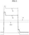
- FIG. 2 is a waveform diagram of a signal applied to a pixel of a liquid crystal display according to an exemplary embodiment of the present disclosure.
- a given one pixel PX that is representative of repeated such pixels, includes a plurality of signal lines passing therethrough or alongside thereof, including a gate line GL provided for conveying a gate signal to gates of plural transistors within the pixel PX, a data line DL provided for transferring a data signal to plural ones of transistors within the pixel PX, and a reference voltage line RL provided for transferring a voltage-dividing reference voltage, where the plural transistors within the pixel PX include a first switching element Qa, a second switching element Qb, and a third switching element Qc.
- the first through third switching elements are connected as shown to the plurality of signal lines, and further to a first liquid crystal capacitor C1cH defined by a first subpixel PEa and to a second liquid crystal capacitor C1cL defined by a first subpixel PEb of the pixel unit PX.
- the first through third switching elements, Qa-Qc each have their respective gates connected to the passing through gate line GL, the first and second switching elements, Qa and Qb are further connected to the corresponding data line DL of the pixel PX while the third switching element Qc is connected to an output (drain) terminal of the second switching element Qb and also to the reference voltage line RL.
- the first switching element Qa and the second switching element Qb are three-terminal field effect elements such as thin film MOSFET transistors and the insulated control terminals (gates) thereof are connected to the gate line GL.
- the source or input terminals of Qa and Qb are connected to the data line DL.
- the output terminal (drain) of the first switching element Qa is connected the first liquid crystal capacitor C1cH (also referenced as Clca occasionally herein).
- the output terminal (drain) of the second switching element Qb is connected to the second liquid crystal capacitor ClcL (also referenced as Clcb occasionally herein) and also to an input terminal (source) of the third switching element Qc.
- the third switching element Qc is also the three-terminal element such as the thin film transistor and a control terminal thereof is connected to the gate line GL, the input terminal is connected to the second liquid crystal capacitor Clcb, and an output terminal thereof is connected to the reference voltage line RL.
- each of Qa, Qb and Qc is an NMOS device.
- each of the first switching element Qa, the second switching element Qb, and the third switching element Qc connected thereto is turned on (a channel region, not shown, within the corresponding transistor is switched into a conductive state).
- a data voltage that is then applied to the data line DL is applied through the turned first and second transistors (Qa and Qb) for application to the first subpixel electrode PEa and to the second subpixel electrode PEb respective through the first and second switching elements, Qa and Qb.
- the data voltages developed at the first subpixel electrode PEa and the second subpixel electrode PEb may be charged to a same value.
- the reference voltage Vr may be different than the supplied data voltage Vd and in such a case, the voltage developed on the second subpixel electrode PEb is a function of Vd as divided by a voltage divider formed by the series combination of the third switching element Qc as connected to the second switching element Qb in series.
- the divider produced voltage, Vb which develops on the second subpixel electrode PEb will be smaller than the voltage Va which develops on the first subpixel electrode PEa in response to the supplied data line voltage Vd.
- the reduced voltage that is charged into the second liquid crystal capacitor Clcb can be made to be approximately equal to and offset plus a divided version (Rc/(Rb+Rc)) of the voltage Va which develops on the first liquid crystal capacitor Clca.
- tilt angles of liquid crystal molecules influenced by the first subpixel can be made to be different from tilt angles of liquid crystal molecules influenced by the second subpixel, and as a result, front versus side visibilities and/or luminances of the respective subpixels can be made different from each other.
- the voltage charged in the first liquid crystal capacitor Clca and the voltage charged in the second liquid crystal capacitor Clcb are appropriately adjusted, an image viewed from the lateral side can be adjusted to be relatively close to an image viewed from the front, thereby improving side visibility to correspond closely with front visibility.
- E is a function of Vr.
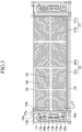
- FIG. 3 is a layout view for one exemplary pixel cell among alike and immediately adjacent and repeated cells of a liquid crystal display corresponding to FIG.1 . Part of a next adjacent cell to the right is also shown.
- FIG. 4 is a cross-sectional view taken along line IV-IV' of FIG. 3 .
- the liquid crystal display includes a lower display panel 100 and an upper display panel 200 that are spaced apart in facing relation with each other, where a liquid crystal material layer 3 is interposed between the two display panels 100 and 200, and where a pair of polarizer plates or sheets (not shown) may be attached or otherwise provided on or adjacent to the outer surfaces of the illustrated display panels 100 and 200.
- a gate line 121 of the repeated cell is positioned directly on an insulation substrate 110 made of a light-passing insulative material such as transparent glass or plastic.
- the gate line 121 extends laterally through the illustrated cell to thereby connect gate electrodes of transistors in left side-area of the full shown cell to gate electrodes of transistors in left side-area of the next adjacent cell (only partly shown).
- the gate line 121 also extends vertically up into the left side-areas of the respective cells.
- the gate line 121 has branches extending contiguously therefrom, including a first gate electrode 124a, a second gate electrode 124b, and a third gate electrode 124c which form respective parts of first through third transistors Qa, Qb and Qc in each left side-area of each respective cell.
- At one or both lateral ends of the gate line 121 there may be provided wide end portions (not shown) for connecting to other interconnect layers of the circuit and/or to external driving circuits.
- a gate insulating layer 140 is positioned on the gate line 121.
- a first semiconductive region 154a, a second semiconductive region 154b, and a third semiconductive region 154c are positioned on the gate insulating layer 140.
- a plurality of ohmic contacts 163a, 165a, 163b, 165b, 163c, and 165c are positioned on the first semiconductive region 154a, the second semiconductive region 154b, and the third semiconductive region 154c.
- a data line 171 extends vertically through the left side-area of the fully illustrated cell on the left.
- the first cell's data line 171 has a plurality of branches extending contiguously therefrom, including a first source electrode 173a a second source electrode 173b and data conductors 173c, 175a, and 175b.
- a reference voltage line 177 also extends vertically through the left side-area of the fully illustrated first cell.
- the reference voltage line 177 has a branch extending contiguously therefrom, namely, third drain electrode 175c. Corresponding portions of the data line 171 and the reference voltage line 177 are positioned on the ohmic contacts 163a, 165a, 163b, 165b, 163c, and 165c and over the gate insulating layer 140.
- the data conductors and the semiconductive regions and the ohmic contacts positioned below the data conductors may be respectively simultaneously formed by using one mask for etching numerous ones of openings through them (e.g., down to the gate insulating layer 140).
- the data line 171 may include at one or both of its terminal ends, respective wide end regions (not shown) for connecting with another interconnect layer and/or external driving circuits.
- the reference voltage line 177 has a giant H-shape in that it includes two vertical portions 177a extending parallel to the data line 171 (one vertical stem of the big H being in the left side-area of the first cell and the other being in the left side-area of the second, only partially-shown cell) and a long horizontal portion 177b connecting both of the vertical portions 177a of the respective left and right side-areas to each other.
- a signal flowing into the reference voltage line 177 may be prevented from being delayed by the horizontal connecting both of the vertical portions 177a of the reference voltage line 177 by means of the laterally extending horizontal portion 177b.
- One of the two vertical portions 177a of the reference voltage line 177 is positioned between the first illustrated subpixel electrode 191a and the data line 171 and it connects with the third drain electrode 175c of respective transistor Qc.
- the horizontal portion 177b of the reference voltage line 177 is positioned to extend under the first cell's two subpixel electrodes, 191a-191b and above the cells' gate line 121 so as to connect to the side-area of the next adjacent cell.
- the reference voltage line 177 may serve as an AC partition wall that reduces signal interference between the charge stored on the pixel electrode 191 and the data lines 171 that run nearby but carry AC signals for charging one row of pixels after the next with different pixel electrode voltages. Also the AC-wise grounded H-structure of the reference voltage line 177 reduces noise coupling from the adjacent gate line 121 to the cells subpixel electrodes 191a-191b.
- the first gate electrode 124a, the first source electrode 173a, and the first drain electrode 175a form the first thin film transistor Qa together with the first semiconductor 154a and a channel of the thin film transistor is formed on the semiconductor 154a between the first source electrode 173a and the first drain electrode 175a.
- the second gate electrode 124b, the second source electrode 173b, and the second drain electrode 175b form the second thin film transistor Qb together with the second semiconductor 154b
- a channel of the thin film transistor is formed on the semiconductor 154b between the second source electrode 173b and the second drain electrode 175b
- the third gate electrode 124c, the third source electrode 173c, and the third drain electrode 175c form the third thin film transistor Qc together with the third semiconductor 154c
- a channel of the thin film transistor is formed on the semiconductor 154c between the third source electrode 173c and the third drain electrode 175c.
- a passivation layer 180 is formed on the data conductors 171, 173c, 175a, 175b, 175c, and 177 and the exposed semiconductors 154a, 154b, and 154c.
- the passivation layer 180 is made of an inorganic insulator such as silicon nitride and silicon oxide.
- the passivation layer 180 may be made of an organic insulator and the top surface of the passivation layer 180 may be planarized.
- the organic insulator may have photosensitivity and a dielectric constant of about 4.0 or less.
- the passivation layer 180 may have a double-layer structure constituted by a lower inorganic layer and an upper organic layer so as to have excellent insulating characteristics and not to damage the exposed semiconductors 154a, 154b, and 154c.
- a plurality of contact holes 185a and 185b exposing the first drain electrode 175a and the second drain electrode 175b are formed through the passivation layer 180.
- a pixel electrode structure 191 including a first subpixel electrode 191a and a second subpixel electrode 191b are formed on the passivation layer 180.
- the pixel electrode structure 191 may be made of a transparent conductive material such as ITO or IZO and/or reflective metal such as aluminum, silver, chromium or an alloy thereof.
- the pixel electrode structure 191 includes a first side extending parallel to the gate line 121 and a second side extending parallel to the data line 171.
- a length of the first side which parallels the gate line 121 is longer than that of the second side parallel to the data line 171, by approximately three times (a 3:1 aspect ratio)
- the number of the pixel electrodes 191 positioned in each row is smaller, but the number of the pixel electrodes 191 positioned in each column is larger than the case that a horizontal side of the pixel-electrode structure is smaller than its vertical side.
- the number of IC chips for providing the data driver function may be decreased, thereby reducing the costs of material and manufacture.
- the number of the gate lines 121 is increased, but since a gate-lines driver may be monolithically integrated on a liquid crystal display panel assembly together with the gate lines 121, as well as with the data lines 171, and the thin film transistors, the increase in number of digitally driven gate lines is not as problematic as when the analog signal outputting data line drivers are increased.
- the cost of the all-digital, gate lines driving IC chip is relatively cheap relative to the mixed mode, digital/analog data line driving IC's, such that it is advantageous to reduce the number of IC chips for the data-lines driver as compared to increasing the number of gate lines and their respective drivers.
- the first subpixel electrode 191a and the second subpixel electrode 191b are adjacent to each other in a row direction of the cell, and in the illustrated embodiment they each in outline have a substantially quadrangular shape, and in their respective interiors they include counter-crossing stem regions or branches branching off from a main horizontal stem 192 and a main vertical stem 193 crossing therewith.
- first subpixel electrode 191a and the second subpixel electrode 191b are divided into four subregions by the horizontal stem 192 and the vertical stem 193 and each subregion includes a plurality of inclined minute branches 194.
- the second subpixel electrode 191b includes a portion that extends along side of at least one side of the first subpixel electrode 191a.
- One of the minute branches 194 of the first subpixel electrode 191a and the second subpixel electrode 191b obliquely extends toward the upper left side from the horizontal stem 192 or the vertical stem 193, and the other of the minute branches 194 obliquely extends toward the upper right side from the horizontal stem 192 or the vertical stem 193.
- another minute branche 194 extends toward the lower left side from the horizontal stem 192 or the vertical stem 193, and the rest one of the minute branches 194 obliquely extends toward the lower right side from the horizontal stem 192 or the vertical stem 193.
- Each of the minute branches 194 forms an angle of approximately 40 to 45 degrees with the gate line 121 or the horizontal stem 192.
- the minute branch 194 included in the first subpixel electrode 191a forms an angle of approximately 40 degrees with the horizontal stem 192 and the minute branch 194 included in the second subpixel electrode 191b forms an angle of approximately 45 degrees with the horizontal stem 192.
- minute branches 194 of adjacent two subregions may be perpendicular to each other.
- the width of the minute branches 194 may be gradually widened as a function of distance so as to create varying domains for orienting the molecules of the local liquid crystal material.
- the first subpixel electrode 191a and the second subpixel electrode 191b are physically and electrically connected with the first drain electrode 175a and the second drain electrode 175b through the contact holes 185a and 185b, respectively, and couple to the applied data line voltage Vd by way of the first drain electrode 175a and the second drain electrode 175b respectively.
- the magnitude of the voltage Vb developed on the second subpixel electrode 191b is smaller than that of the voltage Va developed on the first subpixel electrode 191a.
- the direction that currents flow may be decided by a relation between magnitudes of the reference voltage Vr and the data line voltage Vd.
- the area of the second subpixel electrode 191b is larger than that of the first subpixel electrode 191a by a ratio in one embodiment that is greater than 1 and less than or equal to about 2.
- the area of the second subpixel electrode 191b is between once to about 1.5 times larger than that of the first subpixel electrode 191a and thus the capacitance of the secondary liquid crystal capacitor ClcL is similarly greater than that of the first liquid crystal capacitor ClcH.
- a percentage of the first channel ratio with respect to the sum of the first channel ratio plus the second channel ratio is approximately 60% to 95%.
- the first channel width ratio (of Qb) is greater than the second channel width ratio (of Qc).
- the drain-to-source resistance Rc (of Qc) is greater than the drain-to-source resistance Rb (of Qb).
- the percentage of the first channel ratio with respect to the sum of the first channel ratio and the second channel ratio is in the range of about 70% to 80%. But, the range of about 70% to 80% may be modified. In other words, the percentage of the first channel ratio with respect to the sum of the first channel ratio and the second channel ratio may be decreased for higher visibility or increased for higher transmittance.
- a level of the voltage applied to the reference voltage line shoud be higher than that of a common voltage applied to the common electrode, it is preferable that a difference (Vr-Vcom) between absolute values thereof is about 1V to about 4V.
- the reference voltage Vr is about 8V to 11V.
- a light blocking member 220 is formed on the light-passing upper insulation substrate 210 which may be made of a transparent glass or plastic.
- the light blocking member 220 is also called a black matrix and it blocks undesired light leakage from between areas controlled by pixel-electrodes.
- a plurality of color filters 230 are formed on the substrate 210 and the light blocking member 220.
- the color filters 230 are mostly provided in respective opening regions surrounded by the light blocking member 220 and may be elongated along a column of pixel electrodes 191 so as to provide vertically striped RGB color filtering of the like.
- Each of the color filters 230 may display one of primary colors such as three primary colors such as those of a red, a green and a blue.
- each of the color filters 230 may display not only three primary colors of the red, the green, and the blue but one of a cyan, a magenta, a yellow, and a white based color.
- At least one of the light blocking member 220 and the color filter 230 may be formed on the lower substrate 110.
- a planarizing overcoat 250 may be formed on the color filter 230 and the light blocking member 220.
- the overcoat 250 may be made of an insulating material and may prevent the color filters 230 from being exposed and may provide a planarized flat surface on which the common electrode 270 may be disposed.
- the overcoat 250 may optionally be omitted.
- the common electrode 270 may be formed on the overcoat 250.
- Liquid crystal molecule aligning layers are formed on both surfaces of the display panels 100 and 200 and may be vertical alignment layers.
- Polarizers may be provided on outer surfaces of the display panels 100 and 200, where polarization axes of two polarizers are perpendicular to each other and one polarization axis of them is preferably parallel to the elongation direction of the gate line 121.
- the lower of the two polarizers may be omitted.
- the liquid crystal layer 3 is interposed between two display panels 100 and 200, and the liquid crystal layer 3 includes liquid crystal molecules 31 having negative dielectric anisotropy.
- the liquid crystal molecules 31 of the liquid crystal layer 3 have a pretilt so that a long axis is substantially in parallel to a longitudinal direction of the minute branches of the first and the second subpixel electrodes 191a and 191b and may be aligned to be perpendicular to the surfaces of two display panels 100 and 200 while a driving electric field is not applied.
- the liquid crystal layer 3 further includes alignment assistants including reactive mesogen and the liquid crystal molecules 31 have a pretilt so that a long axis is substantially in parallel to a longitudinal direction of the minute branches of the first and the second subpixel electrodes 191a and 191b due to the alignment assistants.
- the first subpixel electrode 191a and the second subpixel electrode 191b when they receive their corresponding voltages Va and Vb developed from a supplied data line voltage Vd respective generate electric fields extending to the common electrode 270 of the common electrode display panel 200 with the latter receiving the common voltage, thereby determining an orientation of the liquid crystal molecules in the liquid crystal layer 3 between the respective electrodes 191a, 191b, and 270.
- the first and second subpixel electrodes 191a and 191b and the common electrode 270 form liquid crystal capacitors Clca and Clcb to maintain the applied voltage even after the respective thin film transistors (Qa, Qb, Qc) are turned off by a turn-off voltage Voff applied to the corresponding gate line 121.
- sides of the minute branches 194 generate a horizontal field component perpendicular to the side of the minute branches 194 by distorting the electric field and tilt directions of the liquid crystal molecules 31 are determined as a direction determined by the horizontal field component.
- liquid crystal molecules 31 are first tilted in a direction perpendicular to the sides of the minute branches 194.
- the liquid crystal molecules 31 to be tilted in a direction opposite to each other are tilted to be parallel to a longitudinal direction of the minute branches 194.
- the number of tilted directions of the liquid crystal molecules 31 is at least four.
- FIGS. 5 and 6 are graphs showing results of transmittance level (gray level) versus frontal and side visibility of a liquid crystal display according to an Experimental Example structured in accordance with the present disclosure of invention.
- the first subpixel electrode and the second subpixel electrode described in FIGS.1 to 4 may correspond to a high subpixel and a low subpixel to be described below, respectively.
- solid lines indicate transmittance according to a gray in viewing the liquid crystal display from the front and dotted lines with sample point triangles indicate transmittance versus the gray scale when viewing the liquid crystal display from a lateral side (the right side).
- FIG. 6 shows the case of the liquid crystal display according to the exemplary embodiment of the present disclosure where a specific voltage difference (Va > Vb) is induced between the high subpixel and the low subpixel.
- a graph of percent transmittance versus the gray scale and when viewing the liquid crystal display from a lateral side is substantially closer to the graph of transmittance versus the gray scale when viewing the liquid crystal display from the front, and in particular, the slope of transmittance versus gray level more closely mimics the slope of transmittance versus gray level in the lower portion of the gray scale (extending from 0 to 64 in the illustrated example).
- Table 1 shows the display characteristic of the liquid crystal display according to the described experimental examples.
- a desired value of the voltage ratio (Vb/Va) of the high subpixel and the low subpixel may be in the range of about 0.7 to about 0.8, for example.
- the transmittance of the liquid crystal display may be decreased.
- both the transmittance and the lateral side visibility of the liquid crystal display may be increased.
- the transmittance of the liquid crystal display is not decreased and the visibility index is decreased, thereby to improve the lateral side visibility.
- the transmittance is not decreased and the lateral side visibility may be measurably improved.
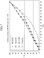
- FIG. 7 is a graph showing variation in transmittance according to a gray for each of sizes of the divided voltage switching elements in the liquid crystal display according to the exemplary embodiment of the present invention.
- FIG. 7 shows variation in transmittance according to variation in voltage ratio of the low subpixel to the high subpixel when the area ratio of the high subpixel and the low subpixel is 1 : 1.25.
- the illustrated 2.2 gamma curve shows transmittance according to a gray in viewing the liquid crystal display from the front side.
- the rest of the curves show transmittance according to a gray in viewing the liquid crystal display from the lateral side.
- FIG. 8 is a graph showing variation in transmittance according to a gray for each of area ratios of the low subpixel to the high subpixel in the liquid crystal display according to the tested exemplary embodiments.
- FIG. 8 shows variation in transmittance according to an area ratio of the low subpixel to the high subpixel when the voltage ratio (Vb/Va) of the low subpixel to the high subpixel is 70%.
- the area ratio of the low subpixel to the high subpixel is increased, it is closer to the graph of the transmittance according to a gray in viewing the liquid crystal display from the front side and when this is considered, the lateral side visibility is improved.
- the effect is further increased at the low gray scale levels.
- FIG. 9 is a graph showing variation in transmittance according to a gray for each area ratio of the low subpixel to the high subpixel in the liquid crystal display according to the tested exemplary embodiments and
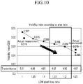
- FIG. 10 is a graph showing a visibility index and transmittance according to area ratio of the low subpixel to the high subpixel in the liquid crystal display according to the exemplary embodiments.
- FIGS. 9 and 10 show the transmittance according to a gray and the visibility index according to the area ratio when the area ratio of the low subpixel to the high subpixel are 1, 1.05, 1.1, 1.15, 1.2, and 1.25 while the channel ratio is 70% and a data voltage of 14.7V is applied.
- the visibility index is decreased and the transmittance is decreased.
- FIG. 11 shows variation in transmittance according to a reference voltage Vref in the liquid crystal display according to the tested exemplary embodiment
- FIG. 12 shows variation in visibility index according to a reference voltage Vref in the liquid crystal display according to the exemplary embodiment.
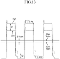
- FIG. 13 is a graph showing distortion of a common voltage generated between the high subpixel and the low subpixel in the liquid crystal display according to the exemplary embodiment.
- FIG. 13 shows a voltage waveform (high) developed at the high subpixel and a voltage waveform (low) developed at the low subpixel.
- the voltage (Vb) applied to the low subpixel is smaller than the voltage (Va) applied to the high subpixel, it swings with a small amplitude around the common voltage.
- the common voltage is a voltage applied to the common electrode formed on the upper display panel.
- a difference h1 between a level of the high subpixel and a level of the low subpixel in a positive polarity mode is different from a difference h2 between a level of the high subpixel and a level of the low subpixel in a negative polarity mode.
- the reason is that a kickback voltage of the low subpixel is larger than that of the high subpixel.
- an amount of the voltage dropped in a positive polarity is different from an amount of the kickback voltage which the voltage is increased in a negative polarity.
- the reference voltage applied through the reference voltage line which is connected with the third thin film transistor may be increased, thereby increasing a voltage Vb developed at the low subpixel.
- the reference voltage may be higher than the common voltage applied to the common electrode and when the common voltage is 7V, the reference voltage Vr may be in the range of 8V to 11V.
- the difference with the level of the common voltage high Vcom corresponding to the high subpixel is reduced by increasing the level of the common voltage Low Vcom corresponding to the low subpixel
- a voltage signal Vr applied to the reference voltage line may be swung.
- the level of the voltage applied to the low subpixel in the positive polarity mode is increased and the level of the voltage applied to the low subpixel in the negative polarity mode is decreased, thereby improving the transmittance.
- the reference voltage signal may be swung.
- the reference voltage may include a signal having a duty ratio which is swung in the range of 50% to 80%.
- the duty ratio is called a ratio of an off time and an on time of the reference voltage while the gate signal is turned on.
- FIG. 14 is a layout view (generally to scale) for one pixel unit or cell of a liquid crystal display according to the other exemplary embodiment and FIG. 15 is a cross-sectional view taken along line XV-XV' of FIG. 14 .
- the liquid crystal display according to the exemplary embodiment has a structure substantially similar (with some exceptions) to the structure of the liquid crystal display according to the exemplary embodiment shown in FIGS. 3 and 4 .
- the liquid crystal display according to the exemplary embodiment further includes a second light blocking unit 127a disposed in the lower substrate below the vertical portion 177a of the reference voltage line 177 and formed on the same layer as the gate line 121, unlike the liquid crystal display according to the exemplary embodiment shown in FIGS. 3 and 4 .
- the light blocking unit 127a prevents the semiconductor 157 disposed below the vertical portion 177a of the reference voltage line 177 from being activated by light for example passed from the backlighting unit so as to thereby more stably maintain a voltage value applied to the reference voltage line 177.
- FIG. 16 is a layout view for one pixel cell of a liquid crystal display according to yet another exemplary embodiment.
- FIG. 17 is a cross-sectional view taken along line XVII-XVII' of FIG. 16 .
- the liquid crystal display according to the exemplary embodiment has a structure similar to the structure of the liquid crystal display according to the exemplary embodiment shown in FIGS. 3 and 4 .
- the liquid crystal display according to the exemplary embodiment further includes a shielding electrode line 88 disposed on the lower substrate and over the gate line 121 and formed on the same layer as the pixel electrode 191, unlike the liquid crystal display according to the exemplary embodiment shown in FIGS. 3 and 4 .
- the shielding electrode line 88 may be made of the same conductive material as that of the pixel-electrode.
- the shielding electrode line 88 has a width larger than the gate line 121 to fully cover the gate line 121.
- a voltage almost similar to the voltage applied to the common electrode 270 may be applied to the shielding electrode line 88 such that irregular movement of the liquid crystal molecules is prevented around the gate line 121 and it is thereby possible to prevent display quality deterioration such as from light leakage by the moved liquid crystal molecules.
- the liquid crystal display may include a shielding electrode (not shown) extended in a vertical direction by being protruded from the illustrated shielding electrode line 88 shown extended in a horizontal direction.
- the shielding electrode may overlap a portion of the gate line connecting the gate electrodes 124a, 124b, and 124c in the gate line 121 extended in a horizontal direction.
- FIG. 18 is a layout view for one pixel of a liquid crystal display according to yet another exemplary embodiment.
- the liquid crystal display according to the exemplary embodiment has a structure similar to the structure of the liquid crystal display according to the exemplary embodiment shown in FIGS. 3 and 4 .
- the liquid crystal display according to the exemplary embodiment is different from overall shapes of the first subpixel electrode 191a and the second subpixel electrode 191b of the liquid crystal display according to the exemplary embodiment shown in FIGS. 3 and 4 .
- the liquid crystal display according to the exemplary embodiment of Fig. 18 includes the first subpixel electrode 191a and the second subpixel electrode 191b divided into a plurality of regions by a first cutout 91.
- the first subpixel electrode 191a divided by the first cutout 91 includes a first region 189a and a second region 189b extended along a tilted direction with respect to the gate line 121 and a connection bridge 189c connecting the first region 189a with the second region 189b.
- the second subpixel electrode 191b divided by the first cutout 91 includes a third region 190a and a fourth region 190b extended along a tilted direction with respect to the gate line 121 and a connection bridge 190c connecting the third region 190a with the fourth region 190b.
- Portions of the first subpixel electrode 191a are surrounded by portions of the second subpixel electrode 191b.
- the common electrode 270 formed on the upper display panel 200 may include a second cutout 71 corresponding to the first cutout 91.
- the second cutout 71 is alternately arranged in position with respect to the first cutout 91.
- the first subpixel electrode 191a and the second subpixel electrode 191b are physically and electrically connected with the first drain electrode 175a and the second drain electrode 175b through the contact holes 185a and 185b, respectively and receive the data voltage from the first drain electrode 175a and the second drain electrode 175b.
- a voltage applied to the second subpixel electrode 191b becomes smaller than a voltage applied to the first subpixel electrode 191a.
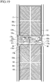
- FIG. 19 is a layout view (generally to scale) for one pixel cell of a liquid crystal display according to yet another exemplary embodiment.
- the liquid crystal display according to the exemplary embodiment has a structure similar to the structure of the liquid crystal display according to the exemplary embodiment shown in FIGS. 3 and 4 .
- the three transistors are disposed in the middle of the pixel-electrode where the pixel electrode has a vertically long form, unlike the exemplary embodiment shown in FIGS. 3 and 4 including the pixel electrode having the horizontally long form.
- the pixel electrode 191 of the exemplary embodiment includes the first subpixel electrode 191a on one side of the three transistors (Qa, Qb, Qc) and the second subpixel electrode 191b on the other side and the outline of the pixel electrode 191 includes a first side parallel to the gate line 121 and a second side parallel to the data line 171.
- the first side parallel to the gate line 121 is shorter than the second side parallel to the data line 171.
- the first thin film transistor Qa, the second thin film transistor Qb, and the third thin film transistor Qc are positioned between the first subpixel electrode 191a and the second subpixel electrode 191b.
- a connection structure of the first thin film transistor Qa, the second thin film transistor Qb, and the third thin film transistor Qc is substantially similar to that of the exemplary embodiment described in FIGS.1 , 3 , and 4 .
- the reference voltage line 177 is positioned on the same layer as the gate line 121 and may be physically and electrically connected through the contact hole 185c of the gate insulating layer 140 which is interposed between the reference voltage line 177 and the data conductors 171, 173c, 175a, 175b, and 175c.
- the liquid crystal display according to the exemplary embodiment includes a shielding electrode line 88p extended in parallel along the data line 171.
- the shielding electrode line 88p may be formed on the same layer as the pixel electrode 191 on the data line 171 and includes a shielding electrode 88 protruded in a direction which the gate line 121 is extended.
- the shielding electrode 88 may be overlapped with an edge portion of the gate line 121.
- the shielding electrode 88 is separated from the pixel electrode 191, particularly, the second subpixel electrode 191b.
- FIG. 20 is a layout view for one pixel of a liquid crystal display according to yet another exemplary embodiment of the present invention.
- the liquid crystal display according to the exemplary embodiment is substantially similar to the structure of the liquid crystal display according to the exemplary embodiment shown in FIG.19 , but is different from the overall shapes of the reference voltage line 177.
- the liquid crystal display according to the exemplary embodiment includes the reference voltage line 177 extending along an extending direction of the vertical stem 193 of the subpixel electrodes 191a, 191b.
- the reference voltage line 177 overlaps the vertical stem 193. But, the reference voltage line 177 goes around not to intersect the second thin film transistor.
- the reference voltage line 177 includes the third drain electrode 175c (an output terminal of the third thin film transistor) facing a large end portion of the third source electrode 173c (an input terminal of the third thin film transistor).
- the reference voltage line 177 is disposed at a same layer as the data line 171. Therefore, the liquid crystal display according to the exemplary embodiment need not form a contact hole 185b as in the exemplary embodiment shown in FIG. 19 .
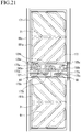
- FIG. 21 is a layout view for one pixel of a liquid crystal display according to yet another exemplary embodiment of the present invention.
- the liquid crystal display according to the exemplary embodiment is substantially similar to the structure of the liquid crystal display according to the exemplary embodiment shown in FIG.19 , but is different from the overall shapes of the first subpixel electrode 191a and the second subpixel electrode 191b.
- the liquid crystal display according to the exemplary embodiment includes the first subpixel electrode 191a and the second subpixel electrode 191b divided into a plurality of regions by a first cutout 91.
- the first subpixel electrode 191a divided by the first cutout 91 includes regions curved in a chevron shape.
- the second subpixel electrode 191b divided by the first cutout 91 includes regions curved in a chevron shape.
- the shape and layout of the first subpixel electrode 191a and the second subpixel electrode 191b are not limited to the exemplary embodiment and may be modified.
- the common electrode 270 formed on the upper display panel 200 includes the second cutout 71 and the second cutout 71 and the first cutout 91 are arranged alternately.
Landscapes
- Physics & Mathematics (AREA)
- Nonlinear Science (AREA)
- General Physics & Mathematics (AREA)
- Crystallography & Structural Chemistry (AREA)
- Chemical & Material Sciences (AREA)
- Engineering & Computer Science (AREA)
- Mathematical Physics (AREA)
- Optics & Photonics (AREA)
- Microelectronics & Electronic Packaging (AREA)
- Geometry (AREA)
- Theoretical Computer Science (AREA)
- Computer Hardware Design (AREA)
- Liquid Crystal (AREA)
- Devices For Indicating Variable Information By Combining Individual Elements (AREA)
Claims (19)
- Afficheur à cristaux liquides, comprenant :un premier substrat (110) ;un deuxième substrat (210) faisant face au premier substrat (110) ;une couche de cristaux liquides (3) interposée entre le premier substrat (110) et le deuxième substrat (210) et incluant des molécules de cristaux liquides (31) ;une ligne de grille (GL ; 121) disposée sur le premier substrat (110) ;une ligne de données (DL ; 171) disposée sur le premier substrat (110) et croisant la ligne de grille (GL ; 121) ;un premier transistor à couche mince (Qa) et un deuxième transistor à couche mince (Qb), les bornes de grille des premier et deuxième transistors à couche mince (Qa ; Qb) étant connectées à la ligne de grille (GL ; 121) et les bornes d'entrée des premier et deuxième transistors à couche mince (Qa ; Qb) étant connectées à la ligne de données (DL ; 171) ;un troisième transistor à couche mince (Qc), la borne de grille du troisième transistor à couche mince (Qc) étant connectée à la ligne de grille (GL ; 121) et la borne d'entrée du troisième transistor à couche mince (Qc) étant connectée à la borne de sortie du deuxième transistor à couche mince (Qb) ;une ligne de tension de référence (RL ; 177) connectée à la borne de sortie du troisième transistor à couche mince (Qc) pour appliquer une tension de référence (Vr) ;une électrode de pixel (191) incluant une première électrode de sous-pixel (PEa ;191a) connectée à la borne de sortie du premier transistor à couche mince (Qa) et une deuxième électrode de sous-pixel (PEb ; 191b) connectée à la borne de sortie du deuxième transistor à couche mince (Qb) ; etune électrode commune (270) positionnée sur le deuxième substrat (210), la borne de sortie du deuxième transistor à couche mince (Qb) étant directement connectée à la borne d'entrée du troisième transistor à couche mince (Qc) ; etla ligne de tension de référence (RL ; 177) étant directement connectée à la borne de sortie du troisième transistor à couche mince (Qc),caractérisé en ce quela valeur absolue de la tension de référence (Vr) appliquée sur la ligne de tension de référence (RL ; 177) est supérieure à celle de la tension commune (Vcom) appliquée à l'électrode commune (270), le rapport entre la largeur de canal et la longueur de canal du deuxième transistor à couche mince (Qb) étant défini comme premier rapport de canal et le rapport entre la largeur de canal et la longueur de canal du troisième transistor à couche mince (Qc) étant défini comme deuxième rapport de canal, et le rapport entre le premier rapport de canal et la somme du premier rapport de canal et du deuxième rapport de canal se situant dans la plage d'environ 70 % à 80 %, et la tension de référence (Vr) comprenant un signal oscillant.
- Afficheur à cristaux liquides selon la revendication 1, dans lequel :
une surface de la deuxième électrode de sous-pixel (PEb ; 191b) est égale ou plus grande qu'une surface de la première électrode de sous-pixel (PEa ; 191a). - Afficheur à cristaux liquides selon la revendication 2, dans lequel :
un rapport entre la surface de la première électrode de sous-pixel (PEa ; 191a) et la surface de la deuxième électrode de sous-pixel (PEb ; 191b) se situe dans la plage d'environ 1:1 à 1:2. - Afficheur à cristaux liquides selon la revendication 1, dans lequel :
la tension de référence (Vr) est dans la plage d'environ 8 V à 11 V et la tension commune (Vcom) est d'environ 7 V. - Afficheur à cristaux liquides selon la revendication 1, dans lequel :
la tension de référence (Vr) inclut un signal ayant un rapport cyclique qui oscille dans la plage d'environ 50 % à 80 %. - Afficheur à cristaux liquides selon la revendication 1, dans lequel :l'électrode de pixel (191) inclut un premier côté parallèle à la ligne de grille (GL ; 121) et un deuxième côté parallèle à la ligne de données (DL ; 171),une longueur du premier côté étant plus longue que celle du deuxième côté.
- Afficheur à cristaux liquides selon la revendication 6, dans lequel :
la première électrode de sous-pixel (PEa ; 191a) et la deuxième électrode de sous-pixel (PEb ; 191b) incluent chacune une tige en forme de croix ayant une tige horizontale (192) et une tige verticale (193) croisant la tige horizontale (192), et une pluralité de petites branches (194) s'étendant à partir de la tige en forme de croix. - Afficheur à cristaux liquides selon la revendication 7, dans lequel :
la première électrode de sous-pixel (PEa ; 191a) et la deuxième électrode de sous-pixel (PEb ; 191b) incluent chacune une pluralité de sous-régions présentant la pluralité de petites branches (194) s'étendant vers différentes directions à partir de la tige en forme de croix. - Afficheur à cristaux liquides selon la revendication 8, dans lequel :
la ligne de tension de référence (RL ; 177) inclut deux parties verticales (177a) parallèles à la ligne de données (DL ; 171) et une partie horizontale (177b) reliant les parties verticales (177a) entre elles. - Afficheur à cristaux liquides selon la revendication 9, dans lequel :
la partie verticale (177a) de la ligne de tension de référence (RL ; 177) est disposée entre l'électrode de pixel (191) et la ligne de données (DL ; 171) et la partie horizontale (177b) de la ligne de tension de référence (RL ; 177) est disposée entre l'électrode de pixel (191) et la ligne de grille (GL ; 121). - Afficheur à cristaux liquides selon la revendication 9, comprenant en outre :
une unité de blocage de lumière (127a) disposée sous la partie verticale (177a) de la ligne de tension de référence (RL ; 177) et formée sur une même couche que la ligne de grille (GL ; 121). - Afficheur à cristaux liquides selon la revendication 11, comprenant en outre :
une électrode de blindage disposée sur une même couche que l'électrode de pixel (191) et chevauchant la ligne de grille (GL ; 121). - Afficheur à cristaux liquides selon la revendication 8, dans lequel la ligne de tension de référence (RL ; 177) s'étend le long d'une direction d'extension de la tige verticale (193) et chevauche la tige verticale (193).
- Afficheur à cristaux liquides selon la revendication 13, dans lequel la ligne de tension de référence (RL ; 177) est disposée sur une même couche que la ligne de données (DL ; 171).
- Afficheur à cristaux liquides selon la revendication 1, dans lequel la première électrode de sous-pixel (PEa ; 191a) et la deuxième électrode de sous-pixel (PEb ; 191b) incluent chacune une première découpe (91), l'électrode commune (270) inclut une deuxième découpe (71), et la première découpe (91) et la deuxième découpe (71) sont disposées en alternance.
- Afficheur à cristaux liquides selon la revendication 1, dans lequel :
la ligne de grille (GL ; 121) transfère un signal de grille et les signaux de grille appliqués aux bornes de commande du premier transistor à couche mince (Qa), du deuxième transistor à couche mince (Qb) et du troisième transistor à couche mince (Qc) sont transférés simultanément. - Afficheur à cristaux liquides selon la revendication 1, dans lequel :
les molécules de cristaux liquides (31) sont alignées verticalement tant qu'un champ électrique n'est pas appliqué. - Afficheur à cristaux liquides selon la revendication 1, comprenant en outre :
une ligne d'électrode de blindage (88) disposée le long d'une direction dans laquelle la ligne de données (DL ; 171) s'étend, la ligne d'électrode de blindage (88) incluant une électrode de blindage en saillie pour chevaucher la ligne de grille (GL ; 121). - Afficheur à cristaux liquides selon la revendication 18, dans lequel :
l'électrode de blindage est séparée de la deuxième électrode de sous-pixel (PEb ; 191b).
Applications Claiming Priority (1)
| Application Number | Priority Date | Filing Date | Title |
|---|---|---|---|
| KR1020100106852A KR101833498B1 (ko) | 2010-10-29 | 2010-10-29 | 액정 표시 장치 |
Publications (2)
| Publication Number | Publication Date |
|---|---|
| EP2447934A1 EP2447934A1 (fr) | 2012-05-02 |
| EP2447934B1 true EP2447934B1 (fr) | 2018-08-29 |
Family
ID=44313127
Family Applications (1)
| Application Number | Title | Priority Date | Filing Date |
|---|---|---|---|
| EP11156369.8A Active EP2447934B1 (fr) | 2010-10-29 | 2011-03-01 | Écran à cristaux liquides |
Country Status (5)
| Country | Link |
|---|---|
| US (3) | US9087490B2 (fr) |
| EP (1) | EP2447934B1 (fr) |
| JP (2) | JP5943552B2 (fr) |
| KR (1) | KR101833498B1 (fr) |
| CN (1) | CN102466935B (fr) |
Families Citing this family (75)
| Publication number | Priority date | Publication date | Assignee | Title |
|---|---|---|---|---|
| KR20120017350A (ko) * | 2010-08-18 | 2012-02-28 | 삼성전자주식회사 | 비틀린 네마틱 모드의 액정 표시 장치 |
| KR101863759B1 (ko) | 2011-09-29 | 2018-06-04 | 삼성디스플레이 주식회사 | 액정 표시 장치 |
| KR101994271B1 (ko) * | 2011-10-12 | 2019-07-01 | 삼성디스플레이 주식회사 | 표시장치 |
| US8952878B2 (en) | 2011-10-14 | 2015-02-10 | Samsung Display Co., Ltd. | Display device |
| KR101944482B1 (ko) * | 2012-01-18 | 2019-02-07 | 삼성디스플레이 주식회사 | 표시 패널 및 이의 구동 방법 |
| KR101973584B1 (ko) * | 2012-02-10 | 2019-04-30 | 삼성디스플레이 주식회사 | 박막 트랜지스터 표시판 및 이를 포함하는 액정 표시 장치 |
| CN102608815A (zh) * | 2012-03-22 | 2012-07-25 | 深圳市华星光电技术有限公司 | 液晶显示面板以及其制造方法 |
| KR20130139548A (ko) | 2012-06-13 | 2013-12-23 | 삼성디스플레이 주식회사 | 액정 표시 장치 |
| KR101991371B1 (ko) * | 2012-06-22 | 2019-06-21 | 삼성디스플레이 주식회사 | 액정 표시 장치 |
| CN102759831B (zh) * | 2012-07-18 | 2015-01-21 | 深圳市华星光电技术有限公司 | 像素结构及相应的液晶显示装置 |
| KR101936923B1 (ko) | 2012-08-22 | 2019-01-10 | 삼성디스플레이 주식회사 | 표시 장치용 모기판, 표시 장치용 모기판의 제조 방법, 및 표시 장치의 제조 방법 |
| KR20140039751A (ko) * | 2012-09-25 | 2014-04-02 | 삼성디스플레이 주식회사 | 표시 장치 및 그 구동 방법 |
| TWI476492B (zh) * | 2012-10-11 | 2015-03-11 | Innocom Tech Shenzhen Co Ltd | 畫素電極結構及使用其之顯示面板 |
| KR101961145B1 (ko) * | 2012-10-17 | 2019-03-26 | 삼성디스플레이 주식회사 | 표시 장치 |
| KR101969954B1 (ko) * | 2012-12-17 | 2019-04-18 | 삼성디스플레이 주식회사 | 액정 표시 장치 |
| KR101995919B1 (ko) * | 2013-01-30 | 2019-07-04 | 삼성디스플레이 주식회사 | 액정 표시 장치 |
| KR102049992B1 (ko) * | 2013-03-12 | 2019-11-29 | 삼성디스플레이 주식회사 | 액정 표시 장치 |
| CN105451767B (zh) | 2013-03-15 | 2019-10-18 | 泽恩格尼亚股份有限公司 | 多价和单价多特异性复合物及其用途 |
| KR102084062B1 (ko) * | 2013-08-26 | 2020-03-04 | 삼성디스플레이 주식회사 | 액정 표시 장치 |
| KR102103501B1 (ko) | 2013-09-16 | 2020-04-23 | 삼성디스플레이 주식회사 | 액정 표시 장치 |
| KR102130110B1 (ko) * | 2013-10-21 | 2020-07-06 | 삼성디스플레이 주식회사 | 표시 패널 및 이의 제조 방법 |
| KR102129569B1 (ko) * | 2013-11-26 | 2020-07-03 | 삼성디스플레이 주식회사 | 액정 표시 장치 |
| CN103700329B (zh) * | 2013-12-13 | 2015-11-11 | 北京京东方光电科技有限公司 | 显示面板的显示方法 |
| KR102159682B1 (ko) * | 2013-12-13 | 2020-10-15 | 삼성디스플레이 주식회사 | 액정 표시 장치 |
| KR102283806B1 (ko) * | 2013-12-17 | 2021-08-03 | 삼성디스플레이 주식회사 | 표시 장치 |
| KR102149345B1 (ko) * | 2013-12-30 | 2020-08-31 | 삼성디스플레이 주식회사 | 액정 표시 장치 및 이의 제조 방법 |
| KR102087379B1 (ko) * | 2013-12-31 | 2020-03-11 | 삼성디스플레이 주식회사 | 액정 표시 장치 |
| KR102188976B1 (ko) * | 2014-01-09 | 2020-12-10 | 삼성디스플레이 주식회사 | 표시 패널 및 이의 구동 방법 |
| KR102183088B1 (ko) * | 2014-02-10 | 2020-11-26 | 삼성디스플레이 주식회사 | 액정 표시 장치 |
| KR20150099665A (ko) * | 2014-02-21 | 2015-09-01 | 삼성디스플레이 주식회사 | 액정 표시 장치 |
| KR102179330B1 (ko) * | 2014-03-18 | 2020-11-18 | 삼성디스플레이 주식회사 | 액정 표시 장치 및 액정 표시 장치의 제조 방법 |
| KR102183921B1 (ko) * | 2014-05-08 | 2020-11-30 | 삼성디스플레이 주식회사 | 액정 표시 장치 |
| TWI526763B (zh) * | 2014-05-13 | 2016-03-21 | 友達光電股份有限公司 | 畫素結構、畫素陣列以及顯示面板 |
| KR20150134465A (ko) * | 2014-05-21 | 2015-12-02 | 삼성디스플레이 주식회사 | 표시 장치 |
| US20150346478A1 (en) * | 2014-05-30 | 2015-12-03 | Qualcomm Mems Technologies, Inc. | Protection of Thin Film Transistors in a Display Element Array from Visible and Ultraviolet Light |
| KR102196451B1 (ko) * | 2014-06-20 | 2020-12-30 | 삼성디스플레이 주식회사 | 액정 표시 장치 |
| KR20160002511A (ko) * | 2014-06-30 | 2016-01-08 | 삼성디스플레이 주식회사 | 표시장치 |
| TWI552320B (zh) * | 2014-08-18 | 2016-10-01 | 群創光電股份有限公司 | 低色偏之顯示面板 |
| KR102243210B1 (ko) * | 2014-08-19 | 2021-04-23 | 삼성디스플레이 주식회사 | 표시 장치 |
| KR20160029892A (ko) * | 2014-09-05 | 2016-03-16 | 삼성디스플레이 주식회사 | 표시 장치 및 그것의 구동 방법 |
| CN204065625U (zh) * | 2014-10-10 | 2014-12-31 | 京东方科技集团股份有限公司 | 一种阵列基板及液晶显示装置 |
| KR20160061536A (ko) * | 2014-11-21 | 2016-06-01 | 삼성디스플레이 주식회사 | 액정 표시 장치 |
| KR102270258B1 (ko) * | 2014-11-28 | 2021-06-28 | 삼성디스플레이 주식회사 | 액정 표시 장치 및 그 구동방법 |
| KR101798433B1 (ko) * | 2014-12-31 | 2017-11-17 | 엘지디스플레이 주식회사 | 인셀 터치 액정 디스플레이 장치와 이의 제조방법 |
| KR20160085387A (ko) * | 2015-01-07 | 2016-07-18 | 삼성디스플레이 주식회사 | 액정 표시 장치 및 그 구동 방법 |
| CN104597648B (zh) * | 2015-01-21 | 2016-11-30 | 深圳市华星光电技术有限公司 | 一种液晶显示面板及装置 |
| KR102308188B1 (ko) * | 2015-02-04 | 2021-10-01 | 삼성디스플레이 주식회사 | 액정 표시 장치 |
| KR102342694B1 (ko) | 2015-02-17 | 2021-12-23 | 삼성디스플레이 주식회사 | 액정 표시 장치 |
| KR102317719B1 (ko) | 2015-02-23 | 2021-10-26 | 삼성디스플레이 주식회사 | 액정 표시 장치 |
| KR102322085B1 (ko) * | 2015-02-23 | 2021-11-04 | 삼성디스플레이 주식회사 | 액정 표시 장치 |
| KR102335825B1 (ko) * | 2015-04-23 | 2021-12-06 | 삼성디스플레이 주식회사 | 액정 표시 장치 |
| KR102351508B1 (ko) * | 2015-04-28 | 2022-01-14 | 삼성디스플레이 주식회사 | 액정 표시 장치 |
| KR102326555B1 (ko) * | 2015-04-29 | 2021-11-17 | 삼성디스플레이 주식회사 | 표시장치 |
| KR102440559B1 (ko) | 2015-06-03 | 2022-09-06 | 삼성디스플레이 주식회사 | 액정 표시 장치 및 액정 표시 장치의 제조 방법 |
| CN104834142A (zh) * | 2015-06-03 | 2015-08-12 | 合肥鑫晟光电科技有限公司 | 像素结构、阵列基板及显示装置 |
| KR102402605B1 (ko) * | 2015-07-28 | 2022-05-27 | 삼성디스플레이 주식회사 | 유기 발광 표시 장치 |
| US9885931B2 (en) * | 2015-09-08 | 2018-02-06 | Boe Technology Group Co., Ltd. | Sub-pixel unit, array substrate and display device |
| CN105182649A (zh) * | 2015-10-29 | 2015-12-23 | 深圳市华星光电技术有限公司 | 广视角面板和显示装置 |
| KR102491239B1 (ko) | 2016-05-03 | 2023-01-25 | 삼성디스플레이 주식회사 | 액정 표시 장치 |
| CN205608389U (zh) * | 2016-05-11 | 2016-09-28 | 重庆京东方光电科技有限公司 | 一种缓存装置及设有该缓存装置的涂胶显影机 |
| KR102566788B1 (ko) * | 2016-06-17 | 2023-08-14 | 삼성디스플레이 주식회사 | 액정 표시 장치 |
| CN106019747A (zh) * | 2016-07-26 | 2016-10-12 | 京东方科技集团股份有限公司 | 一种阵列基板、其驱动方法及显示面板 |
| KR102599255B1 (ko) | 2016-08-10 | 2023-11-07 | 삼성디스플레이 주식회사 | 액정 표시 장치 |
| KR102596770B1 (ko) * | 2016-12-05 | 2023-11-01 | 삼성디스플레이 주식회사 | 액정 표시 장치 |
| TWI637624B (zh) | 2017-05-09 | 2018-10-01 | 友達光電股份有限公司 | 畫素陣列 |
| KR102367963B1 (ko) * | 2017-07-13 | 2022-02-25 | 삼성디스플레이 주식회사 | 액정 표시 장치 |
| CN107561803A (zh) * | 2017-09-22 | 2018-01-09 | 惠科股份有限公司 | 像素结构 |
| CN107728352B (zh) * | 2017-11-22 | 2020-05-05 | 深圳市华星光电半导体显示技术有限公司 | 一种像素驱动电路及液晶显示面板 |
| CN108597374B (zh) * | 2018-04-20 | 2021-02-02 | 上海天马有机发光显示技术有限公司 | 一种显示面板和显示装置 |
| TWI683427B (zh) | 2018-08-15 | 2020-01-21 | 友達光電股份有限公司 | 畫素結構 |
| US11092858B2 (en) * | 2018-09-26 | 2021-08-17 | Xianyang Caihong Optoelectronics Technology Co., Ltd | Pixel structure and pixel unit |
| KR20200056517A (ko) * | 2018-11-14 | 2020-05-25 | 삼성디스플레이 주식회사 | 표시 장치 |
| KR20200133043A (ko) * | 2019-05-15 | 2020-11-26 | 삼성디스플레이 주식회사 | 액정 표시 장치 |
| CN111308808B (zh) * | 2020-04-01 | 2021-05-07 | 深圳市华星光电半导体显示技术有限公司 | 像素电极及液晶显示面板 |
| KR20220018117A (ko) * | 2020-08-05 | 2022-02-15 | 삼성디스플레이 주식회사 | 표시 장치 |
Family Cites Families (37)
| Publication number | Priority date | Publication date | Assignee | Title |
|---|---|---|---|---|
| KR100205259B1 (ko) | 1996-03-04 | 1999-07-01 | 구자홍 | 액티브매트릭스 액정디스플레이의 구동회로 |
| JP2735070B2 (ja) | 1996-04-15 | 1998-04-02 | 日本電気株式会社 | アクティブマトリクス液晶表示パネル |
| KR100272284B1 (ko) | 1998-08-24 | 2000-11-15 | 구본준 | 디멀티플렉서 및 그를 이용한 액정 패널 |
| JP4019593B2 (ja) | 1999-02-24 | 2007-12-12 | セイコーエプソン株式会社 | 電気光学装置および電子機器 |
| CN1198172C (zh) * | 1999-12-03 | 2005-04-20 | 三菱电机株式会社 | 液晶显示装置 |
| KR100743101B1 (ko) | 2001-05-07 | 2007-07-27 | 엘지.필립스 엘시디 주식회사 | 액정표시장치 및 그 제조방법과 이를 이용한 화소리페어방법 |
| JP4551049B2 (ja) | 2002-03-19 | 2010-09-22 | 三菱電機株式会社 | 表示装置 |
| JP2004205855A (ja) | 2002-12-25 | 2004-07-22 | Sharp Corp | 液晶表示装置 |
| KR100564218B1 (ko) | 2003-12-11 | 2006-03-28 | 엘지.필립스 엘시디 주식회사 | 횡전계형 액정표시장치용 기판 및 그 제조 방법 |
| JP4578915B2 (ja) | 2004-09-30 | 2010-11-10 | シャープ株式会社 | アクティブマトリクス型液晶表示装置およびそれに用いる液晶表示パネル |
| JP4571845B2 (ja) | 2004-11-08 | 2010-10-27 | シャープ株式会社 | 液晶表示装置用基板及びそれを備えた液晶表示装置及びその駆動方法 |
| US8068200B2 (en) | 2004-12-24 | 2011-11-29 | Casio Computer Co., Ltd. | Vertical alignment liquid crystal display device in which a pixel electrode has slits which divide the pixel electrode into electrode portions |
| JP4829501B2 (ja) | 2005-01-06 | 2011-12-07 | シャープ株式会社 | 液晶表示装置 |
| KR101133760B1 (ko) * | 2005-01-17 | 2012-04-09 | 삼성전자주식회사 | 박막 트랜지스터 표시판 및 이를 포함하는 액정 표시 장치 |
| US8243105B2 (en) | 2005-03-15 | 2012-08-14 | Sharp Kabushiki Kaisha | Display device, display device adjustment method, image display monitor, and television receiver |
| KR101171180B1 (ko) * | 2005-07-15 | 2012-08-20 | 삼성전자주식회사 | 액정 표시 장치 |
| KR101152135B1 (ko) | 2005-09-12 | 2012-06-15 | 삼성전자주식회사 | 액정 표시 장치 및 그 구동 방법 |
| US7576720B2 (en) * | 2005-11-30 | 2009-08-18 | Au Optronics Corporation | Transflective liquid crystal display |
| JP5329053B2 (ja) | 2006-05-24 | 2013-10-30 | 三星ディスプレイ株式會社 | 表示基板 |
| KR101349092B1 (ko) | 2006-09-07 | 2014-01-09 | 삼성디스플레이 주식회사 | 어레이 기판 및 이를 갖는 표시장치 |
| JP4949908B2 (ja) | 2007-03-29 | 2012-06-13 | 富士フイルム株式会社 | 放射線画像検出方法および装置 |
| JP5542296B2 (ja) * | 2007-05-17 | 2014-07-09 | 株式会社半導体エネルギー研究所 | 液晶表示装置、表示モジュール及び電子機器 |
| KR101634970B1 (ko) | 2007-05-18 | 2016-06-30 | 가부시키가이샤 한도오따이 에네루기 켄큐쇼 | 반도체 장치 및 반도체 장치 제조 방법 |
| US8174636B2 (en) | 2007-08-10 | 2012-05-08 | Chimei Innolux Corporation | Thin film transistor substrate and liquid crystal display having the same comprising a coupling capacitor as a voltage divider between a TFT and a data line |
| KR101515085B1 (ko) | 2007-10-22 | 2015-05-04 | 삼성디스플레이 주식회사 | 액정 표시 장치 |
| KR101450887B1 (ko) | 2007-12-28 | 2014-10-14 | 엘지디스플레이 주식회사 | 유기전계발광표시장치 |
| KR101448001B1 (ko) | 2008-01-29 | 2014-10-13 | 삼성디스플레이 주식회사 | 액정 표시 장치 |
| CN100593752C (zh) | 2008-02-29 | 2010-03-10 | 上海广电光电子有限公司 | 液晶显示面板、像素结构及其制造方法 |
| TWI387827B (zh) | 2008-03-12 | 2013-03-01 | Chunghwa Picture Tubes Ltd | 多域垂直配向型(mva)畫素結構 |
| KR101490475B1 (ko) | 2008-06-25 | 2015-02-06 | 삼성디스플레이 주식회사 | 액정 표시 장치 및 액정 표시 장치의 구동 방법 |
| JP2010060967A (ja) | 2008-09-05 | 2010-03-18 | Epson Imaging Devices Corp | 液晶表示装置及び電子機器 |
| RU2475791C1 (ru) | 2009-02-13 | 2013-02-20 | Шарп Кабусики Кайся | Подложка матрицы, жидкокристаллическое устройство отображения, электронное устройство |
| GB2470752B (en) * | 2009-06-03 | 2015-01-07 | Au Optronics Corp | Autostereoscopic Display Apparatus |
| RU2511709C2 (ru) * | 2009-06-30 | 2014-04-10 | Шарп Кабусики Кайся | Жидкокристаллическое устройство отображения |
| US9007284B2 (en) * | 2009-07-30 | 2015-04-14 | Sharp Kabushiki Kaisha | Liquid crystal display element, liquid crystal display device, and display method employed in liquid crystal display element |
| KR101695474B1 (ko) * | 2009-10-28 | 2017-01-13 | 삼성디스플레이 주식회사 | 액정 표시 장치 |
| KR101659831B1 (ko) | 2010-04-22 | 2016-09-27 | 삼성디스플레이 주식회사 | 액정표시장치, 이를 구동하는 방법 및 이의 제조 방법 |
-
2010
- 2010-10-29 KR KR1020100106852A patent/KR101833498B1/ko active IP Right Grant
-
2011
- 2011-02-17 US US13/029,968 patent/US9087490B2/en active Active
- 2011-03-01 EP EP11156369.8A patent/EP2447934B1/fr active Active
- 2011-04-11 CN CN201110089192.4A patent/CN102466935B/zh active Active
- 2011-05-19 JP JP2011112245A patent/JP5943552B2/ja active Active
-
2015
- 2015-07-17 US US14/802,778 patent/US9341907B2/en active Active
- 2015-09-24 JP JP2015186790A patent/JP6093824B2/ja active Active
-
2016
- 2016-05-11 US US15/151,699 patent/US9606406B2/en active Active
Also Published As
| Publication number | Publication date |
|---|---|
| CN102466935B (zh) | 2016-04-20 |
| JP2016026320A (ja) | 2016-02-12 |
| KR20120060996A (ko) | 2012-06-12 |
| US20150323847A1 (en) | 2015-11-12 |
| JP2012098695A (ja) | 2012-05-24 |
| JP5943552B2 (ja) | 2016-07-05 |
| US9087490B2 (en) | 2015-07-21 |
| US20120105785A1 (en) | 2012-05-03 |
| US9341907B2 (en) | 2016-05-17 |
| KR101833498B1 (ko) | 2018-03-02 |
| US20160252795A1 (en) | 2016-09-01 |
| JP6093824B2 (ja) | 2017-03-08 |
| EP2447934A1 (fr) | 2012-05-02 |
| CN102466935A (zh) | 2012-05-23 |
| US9606406B2 (en) | 2017-03-28 |
Similar Documents
| Publication | Publication Date | Title |
|---|---|---|
| EP2447934B1 (fr) | Écran à cristaux liquides | |
| KR101820796B1 (ko) | 액정 표시 장치 | |
| US7796221B2 (en) | Liquid crystal display device and method of preventing image sticking thereon | |
| US8848151B2 (en) | Liquid crystal display device | |
| US7113233B2 (en) | Thin film transistor array panel with varying coupling capacitance between first and second pixel electrodes | |
| US7973864B2 (en) | Liquid crystal display | |
| US7839369B2 (en) | Liquid crystal display having cutout arranged at pixel electrode with specific position from cutout arranged at common electrode, and driving method thereof | |
| US7764329B2 (en) | MVA LCD device and pixel circuit thereof | |
| US20160033834A1 (en) | Liquid crsytal display | |
| US7656487B2 (en) | Liquid crystal display | |
| US8605242B2 (en) | Liquid crystal display | |
| US7973899B2 (en) | Thin film transistor array panel with capacitive coupling between adjacent pixel areas | |
| US9632376B2 (en) | Liquid crystal display device including switching element with floating terminal | |
| KR20110046124A (ko) | 액정 표시 장치 | |
| US9625780B2 (en) | Liquid crystal display | |
| US8045079B2 (en) | Display device | |
| KR20130042242A (ko) | 액정 표시 장치 | |
| US9786237B2 (en) | Liquid crystal display | |
| KR102353725B1 (ko) | 액정 표시 장치 | |
| US20160216577A1 (en) | Liquid crystal display |
Legal Events
| Date | Code | Title | Description |
|---|---|---|---|
| PUAI | Public reference made under article 153(3) epc to a published international application that has entered the european phase |
Free format text: ORIGINAL CODE: 0009012 |
|
| AK | Designated contracting states |
Kind code of ref document: A1 Designated state(s): AL AT BE BG CH CY CZ DE DK EE ES FI FR GB GR HR HU IE IS IT LI LT LU LV MC MK MT NL NO PL PT RO RS SE SI SK SM TR |
|
| AX | Request for extension of the european patent |
Extension state: BA ME |
|
| 17P | Request for examination filed |
Effective date: 20120329 |
|
| RAP1 | Party data changed (applicant data changed or rights of an application transferred) |
Owner name: SAMSUNG ELECTRONICS CO., LTD. |
|
| RAP1 | Party data changed (applicant data changed or rights of an application transferred) |
Owner name: SAMSUNG DISPLAY CO., LTD. |
|
| 17Q | First examination report despatched |
Effective date: 20141205 |
|
| RAP1 | Party data changed (applicant data changed or rights of an application transferred) |
Owner name: SAMSUNG DISPLAY CO., LTD. |
|
| GRAP | Despatch of communication of intention to grant a patent |
Free format text: ORIGINAL CODE: EPIDOSNIGR1 |
|
| STAA | Information on the status of an ep patent application or granted ep patent |
Free format text: STATUS: GRANT OF PATENT IS INTENDED |
|
| INTG | Intention to grant announced |
Effective date: 20180320 |
|
| GRAS | Grant fee paid |
Free format text: ORIGINAL CODE: EPIDOSNIGR3 |
|
| GRAA | (expected) grant |
Free format text: ORIGINAL CODE: 0009210 |
|
| STAA | Information on the status of an ep patent application or granted ep patent |
Free format text: STATUS: THE PATENT HAS BEEN GRANTED |
|
| AK | Designated contracting states |
Kind code of ref document: B1 Designated state(s): AL AT BE BG CH CY CZ DE DK EE ES FI FR GB GR HR HU IE IS IT LI LT LU LV MC MK MT NL NO PL PT RO RS SE SI SK SM TR |
|
| REG | Reference to a national code |
Ref country code: GB Ref legal event code: FG4D |
|
| REG | Reference to a national code |
Ref country code: CH Ref legal event code: EP |
|
| REG | Reference to a national code |
Ref country code: AT Ref legal event code: REF Ref document number: 1036085 Country of ref document: AT Kind code of ref document: T Effective date: 20180915 |
|
| REG | Reference to a national code |
Ref country code: IE Ref legal event code: FG4D |
|
| REG | Reference to a national code |
Ref country code: DE Ref legal event code: R096 Ref document number: 602011051463 Country of ref document: DE |
|
| REG | Reference to a national code |
Ref country code: NL Ref legal event code: MP Effective date: 20180829 |
|
| REG | Reference to a national code |
Ref country code: LT Ref legal event code: MG4D |
|
| PG25 | Lapsed in a contracting state [announced via postgrant information from national office to epo] |
Ref country code: NO Free format text: LAPSE BECAUSE OF FAILURE TO SUBMIT A TRANSLATION OF THE DESCRIPTION OR TO PAY THE FEE WITHIN THE PRESCRIBED TIME-LIMIT Effective date: 20181129 Ref country code: SE Free format text: LAPSE BECAUSE OF FAILURE TO SUBMIT A TRANSLATION OF THE DESCRIPTION OR TO PAY THE FEE WITHIN THE PRESCRIBED TIME-LIMIT Effective date: 20180829 Ref country code: IS Free format text: LAPSE BECAUSE OF FAILURE TO SUBMIT A TRANSLATION OF THE DESCRIPTION OR TO PAY THE FEE WITHIN THE PRESCRIBED TIME-LIMIT Effective date: 20181229 Ref country code: RS Free format text: LAPSE BECAUSE OF FAILURE TO SUBMIT A TRANSLATION OF THE DESCRIPTION OR TO PAY THE FEE WITHIN THE PRESCRIBED TIME-LIMIT Effective date: 20180829 Ref country code: FI Free format text: LAPSE BECAUSE OF FAILURE TO SUBMIT A TRANSLATION OF THE DESCRIPTION OR TO PAY THE FEE WITHIN THE PRESCRIBED TIME-LIMIT Effective date: 20180829 Ref country code: LT Free format text: LAPSE BECAUSE OF FAILURE TO SUBMIT A TRANSLATION OF THE DESCRIPTION OR TO PAY THE FEE WITHIN THE PRESCRIBED TIME-LIMIT Effective date: 20180829 Ref country code: NL Free format text: LAPSE BECAUSE OF FAILURE TO SUBMIT A TRANSLATION OF THE DESCRIPTION OR TO PAY THE FEE WITHIN THE PRESCRIBED TIME-LIMIT Effective date: 20180829 Ref country code: GR Free format text: LAPSE BECAUSE OF FAILURE TO SUBMIT A TRANSLATION OF THE DESCRIPTION OR TO PAY THE FEE WITHIN THE PRESCRIBED TIME-LIMIT Effective date: 20181130 Ref country code: BG Free format text: LAPSE BECAUSE OF FAILURE TO SUBMIT A TRANSLATION OF THE DESCRIPTION OR TO PAY THE FEE WITHIN THE PRESCRIBED TIME-LIMIT Effective date: 20181129 |
|
| REG | Reference to a national code |
Ref country code: AT Ref legal event code: MK05 Ref document number: 1036085 Country of ref document: AT Kind code of ref document: T Effective date: 20180829 |
|
| PG25 | Lapsed in a contracting state [announced via postgrant information from national office to epo] |
Ref country code: AL Free format text: LAPSE BECAUSE OF FAILURE TO SUBMIT A TRANSLATION OF THE DESCRIPTION OR TO PAY THE FEE WITHIN THE PRESCRIBED TIME-LIMIT Effective date: 20180829 Ref country code: ES Free format text: LAPSE BECAUSE OF FAILURE TO SUBMIT A TRANSLATION OF THE DESCRIPTION OR TO PAY THE FEE WITHIN THE PRESCRIBED TIME-LIMIT Effective date: 20180829 Ref country code: HR Free format text: LAPSE BECAUSE OF FAILURE TO SUBMIT A TRANSLATION OF THE DESCRIPTION OR TO PAY THE FEE WITHIN THE PRESCRIBED TIME-LIMIT Effective date: 20180829 Ref country code: LV Free format text: LAPSE BECAUSE OF FAILURE TO SUBMIT A TRANSLATION OF THE DESCRIPTION OR TO PAY THE FEE WITHIN THE PRESCRIBED TIME-LIMIT Effective date: 20180829 |
|
| PG25 | Lapsed in a contracting state [announced via postgrant information from national office to epo] |
Ref country code: EE Free format text: LAPSE BECAUSE OF FAILURE TO SUBMIT A TRANSLATION OF THE DESCRIPTION OR TO PAY THE FEE WITHIN THE PRESCRIBED TIME-LIMIT Effective date: 20180829 Ref country code: PL Free format text: LAPSE BECAUSE OF FAILURE TO SUBMIT A TRANSLATION OF THE DESCRIPTION OR TO PAY THE FEE WITHIN THE PRESCRIBED TIME-LIMIT Effective date: 20180829 Ref country code: CZ Free format text: LAPSE BECAUSE OF FAILURE TO SUBMIT A TRANSLATION OF THE DESCRIPTION OR TO PAY THE FEE WITHIN THE PRESCRIBED TIME-LIMIT Effective date: 20180829 Ref country code: RO Free format text: LAPSE BECAUSE OF FAILURE TO SUBMIT A TRANSLATION OF THE DESCRIPTION OR TO PAY THE FEE WITHIN THE PRESCRIBED TIME-LIMIT Effective date: 20180829 Ref country code: AT Free format text: LAPSE BECAUSE OF FAILURE TO SUBMIT A TRANSLATION OF THE DESCRIPTION OR TO PAY THE FEE WITHIN THE PRESCRIBED TIME-LIMIT Effective date: 20180829 Ref country code: IT Free format text: LAPSE BECAUSE OF FAILURE TO SUBMIT A TRANSLATION OF THE DESCRIPTION OR TO PAY THE FEE WITHIN THE PRESCRIBED TIME-LIMIT Effective date: 20180829 |
|
| PG25 | Lapsed in a contracting state [announced via postgrant information from national office to epo] |
Ref country code: SK Free format text: LAPSE BECAUSE OF FAILURE TO SUBMIT A TRANSLATION OF THE DESCRIPTION OR TO PAY THE FEE WITHIN THE PRESCRIBED TIME-LIMIT Effective date: 20180829 Ref country code: SM Free format text: LAPSE BECAUSE OF FAILURE TO SUBMIT A TRANSLATION OF THE DESCRIPTION OR TO PAY THE FEE WITHIN THE PRESCRIBED TIME-LIMIT Effective date: 20180829 Ref country code: DK Free format text: LAPSE BECAUSE OF FAILURE TO SUBMIT A TRANSLATION OF THE DESCRIPTION OR TO PAY THE FEE WITHIN THE PRESCRIBED TIME-LIMIT Effective date: 20180829 |
|
| REG | Reference to a national code |
Ref country code: DE Ref legal event code: R097 Ref document number: 602011051463 Country of ref document: DE |
|
| PLBE | No opposition filed within time limit |
Free format text: ORIGINAL CODE: 0009261 |
|
| STAA | Information on the status of an ep patent application or granted ep patent |
Free format text: STATUS: NO OPPOSITION FILED WITHIN TIME LIMIT |
|
| 26N | No opposition filed |
Effective date: 20190531 |
|
| PG25 | Lapsed in a contracting state [announced via postgrant information from national office to epo] |
Ref country code: SI Free format text: LAPSE BECAUSE OF FAILURE TO SUBMIT A TRANSLATION OF THE DESCRIPTION OR TO PAY THE FEE WITHIN THE PRESCRIBED TIME-LIMIT Effective date: 20180829 |
|
| PG25 | Lapsed in a contracting state [announced via postgrant information from national office to epo] |
Ref country code: MC Free format text: LAPSE BECAUSE OF FAILURE TO SUBMIT A TRANSLATION OF THE DESCRIPTION OR TO PAY THE FEE WITHIN THE PRESCRIBED TIME-LIMIT Effective date: 20180829 |
|
| REG | Reference to a national code |
Ref country code: CH Ref legal event code: PL |
|
| GBPC | Gb: european patent ceased through non-payment of renewal fee |
Effective date: 20190301 |
|
| PG25 | Lapsed in a contracting state [announced via postgrant information from national office to epo] |
Ref country code: LU Free format text: LAPSE BECAUSE OF NON-PAYMENT OF DUE FEES Effective date: 20190301 |
|
| REG | Reference to a national code |
Ref country code: BE Ref legal event code: MM Effective date: 20190331 |
|
| PG25 | Lapsed in a contracting state [announced via postgrant information from national office to epo] |
Ref country code: CH Free format text: LAPSE BECAUSE OF NON-PAYMENT OF DUE FEES Effective date: 20190331 Ref country code: LI Free format text: LAPSE BECAUSE OF NON-PAYMENT OF DUE FEES Effective date: 20190331 Ref country code: IE Free format text: LAPSE BECAUSE OF NON-PAYMENT OF DUE FEES Effective date: 20190301 Ref country code: GB Free format text: LAPSE BECAUSE OF NON-PAYMENT OF DUE FEES Effective date: 20190301 |
|
| PG25 | Lapsed in a contracting state [announced via postgrant information from national office to epo] |
Ref country code: FR Free format text: LAPSE BECAUSE OF NON-PAYMENT OF DUE FEES Effective date: 20190331 Ref country code: BE Free format text: LAPSE BECAUSE OF NON-PAYMENT OF DUE FEES Effective date: 20190331 |
|
| PG25 | Lapsed in a contracting state [announced via postgrant information from national office to epo] |
Ref country code: TR Free format text: LAPSE BECAUSE OF FAILURE TO SUBMIT A TRANSLATION OF THE DESCRIPTION OR TO PAY THE FEE WITHIN THE PRESCRIBED TIME-LIMIT Effective date: 20180829 |
|
| PG25 | Lapsed in a contracting state [announced via postgrant information from national office to epo] |
Ref country code: MT Free format text: LAPSE BECAUSE OF NON-PAYMENT OF DUE FEES Effective date: 20190301 Ref country code: PT Free format text: LAPSE BECAUSE OF FAILURE TO SUBMIT A TRANSLATION OF THE DESCRIPTION OR TO PAY THE FEE WITHIN THE PRESCRIBED TIME-LIMIT Effective date: 20181229 |
|
| PG25 | Lapsed in a contracting state [announced via postgrant information from national office to epo] |
Ref country code: CY Free format text: LAPSE BECAUSE OF FAILURE TO SUBMIT A TRANSLATION OF THE DESCRIPTION OR TO PAY THE FEE WITHIN THE PRESCRIBED TIME-LIMIT Effective date: 20180829 |
|
| PG25 | Lapsed in a contracting state [announced via postgrant information from national office to epo] |
Ref country code: HU Free format text: LAPSE BECAUSE OF FAILURE TO SUBMIT A TRANSLATION OF THE DESCRIPTION OR TO PAY THE FEE WITHIN THE PRESCRIBED TIME-LIMIT; INVALID AB INITIO Effective date: 20110301 |
|
| PG25 | Lapsed in a contracting state [announced via postgrant information from national office to epo] |
Ref country code: MK Free format text: LAPSE BECAUSE OF FAILURE TO SUBMIT A TRANSLATION OF THE DESCRIPTION OR TO PAY THE FEE WITHIN THE PRESCRIBED TIME-LIMIT Effective date: 20180829 |
|
| P01 | Opt-out of the competence of the unified patent court (upc) registered |
Effective date: 20230515 |
|
| PGFP | Annual fee paid to national office [announced via postgrant information from national office to epo] |
Ref country code: DE Payment date: 20240220 Year of fee payment: 14 |