EP2432817B1 - Polymères conjugués et leur utilisation dans des dispositifs opto-électroniques - Google Patents
Polymères conjugués et leur utilisation dans des dispositifs opto-électroniques Download PDFInfo
- Publication number
- EP2432817B1 EP2432817B1 EP10722246.5A EP10722246A EP2432817B1 EP 2432817 B1 EP2432817 B1 EP 2432817B1 EP 10722246 A EP10722246 A EP 10722246A EP 2432817 B1 EP2432817 B1 EP 2432817B1
- Authority
- EP
- European Patent Office
- Prior art keywords
- group
- alkyl group
- copolymer
- independently
- electrode
- Prior art date
- Legal status (The legal status is an assumption and is not a legal conclusion. Google has not performed a legal analysis and makes no representation as to the accuracy of the status listed.)
- Active
Links
- 230000005693 optoelectronics Effects 0.000 title claims description 11
- 229920000547 conjugated polymer Polymers 0.000 title 1
- 150000001875 compounds Chemical class 0.000 claims description 84
- -1 fullerene compound Chemical class 0.000 claims description 82
- 125000000217 alkyl group Chemical group 0.000 claims description 73
- 239000000463 material Substances 0.000 claims description 60
- 239000000203 mixture Substances 0.000 claims description 48
- 239000004065 semiconductor Substances 0.000 claims description 44
- 229920001577 copolymer Polymers 0.000 claims description 43
- 238000006243 chemical reaction Methods 0.000 claims description 32
- 125000001188 haloalkyl group Chemical group 0.000 claims description 24
- 125000001072 heteroaryl group Chemical group 0.000 claims description 23
- 239000000758 substrate Substances 0.000 claims description 18
- 230000003287 optical effect Effects 0.000 claims description 16
- 125000005842 heteroatom Chemical group 0.000 claims description 14
- 125000003545 alkoxy group Chemical group 0.000 claims description 13
- 229910003472 fullerene Inorganic materials 0.000 claims description 13
- 238000013086 organic photovoltaic Methods 0.000 claims description 12
- 229910052717 sulfur Inorganic materials 0.000 claims description 10
- 229910052760 oxygen Inorganic materials 0.000 claims description 9
- 238000006116 polymerization reaction Methods 0.000 claims description 9
- 125000004414 alkyl thio group Chemical group 0.000 claims description 6
- 239000010409 thin film Substances 0.000 claims description 5
- 229920000642 polymer Polymers 0.000 description 50
- OKKJLVBELUTLKV-UHFFFAOYSA-N Methanol Chemical compound OC OKKJLVBELUTLKV-UHFFFAOYSA-N 0.000 description 42
- 239000010410 layer Substances 0.000 description 40
- VLKZOEOYAKHREP-UHFFFAOYSA-N n-Hexane Chemical class CCCCCC VLKZOEOYAKHREP-UHFFFAOYSA-N 0.000 description 40
- HEDRZPFGACZZDS-UHFFFAOYSA-N Chloroform Chemical compound ClC(Cl)Cl HEDRZPFGACZZDS-UHFFFAOYSA-N 0.000 description 38
- WYURNTSHIVDZCO-UHFFFAOYSA-N Tetrahydrofuran Chemical compound C1CCOC1 WYURNTSHIVDZCO-UHFFFAOYSA-N 0.000 description 38
- HEDRZPFGACZZDS-MICDWDOJSA-N Trichloro(2H)methane Chemical compound [2H]C(Cl)(Cl)Cl HEDRZPFGACZZDS-MICDWDOJSA-N 0.000 description 32
- 125000003118 aryl group Chemical group 0.000 description 31
- 239000000243 solution Substances 0.000 description 31
- 238000002360 preparation method Methods 0.000 description 29
- IJGRMHOSHXDMSA-UHFFFAOYSA-N Atomic nitrogen Chemical compound N#N IJGRMHOSHXDMSA-UHFFFAOYSA-N 0.000 description 28
- 238000000034 method Methods 0.000 description 28
- 239000002904 solvent Substances 0.000 description 28
- 125000003342 alkenyl group Chemical group 0.000 description 23
- RTZKZFJDLAIYFH-UHFFFAOYSA-N Diethyl ether Chemical compound CCOCC RTZKZFJDLAIYFH-UHFFFAOYSA-N 0.000 description 21
- YLQBMQCUIZJEEH-UHFFFAOYSA-N Furan Chemical compound C=1C=COC=1 YLQBMQCUIZJEEH-UHFFFAOYSA-N 0.000 description 21
- YMWUJEATGCHHMB-UHFFFAOYSA-N Dichloromethane Chemical compound ClCCl YMWUJEATGCHHMB-UHFFFAOYSA-N 0.000 description 20
- 229910052757 nitrogen Inorganic materials 0.000 description 18
- 238000005160 1H NMR spectroscopy Methods 0.000 description 17
- XMWRBQBLMFGWIX-UHFFFAOYSA-N C60 fullerene Chemical compound C12=C3C(C4=C56)=C7C8=C5C5=C9C%10=C6C6=C4C1=C1C4=C6C6=C%10C%10=C9C9=C%11C5=C8C5=C8C7=C3C3=C7C2=C1C1=C2C4=C6C4=C%10C6=C9C9=C%11C5=C5C8=C3C3=C7C1=C1C2=C4C6=C2C9=C5C3=C12 XMWRBQBLMFGWIX-UHFFFAOYSA-N 0.000 description 17
- 125000000304 alkynyl group Chemical group 0.000 description 16
- MVPPADPHJFYWMZ-UHFFFAOYSA-N chlorobenzene Chemical compound ClC1=CC=CC=C1 MVPPADPHJFYWMZ-UHFFFAOYSA-N 0.000 description 16
- 239000007787 solid Substances 0.000 description 16
- URMVZUQDPPDABD-UHFFFAOYSA-N thieno[2,3-f][1]benzothiole Chemical compound C1=C2SC=CC2=CC2=C1C=CS2 URMVZUQDPPDABD-UHFFFAOYSA-N 0.000 description 16
- 125000004432 carbon atom Chemical group C* 0.000 description 15
- 125000001424 substituent group Chemical group 0.000 description 15
- 229910001868 water Inorganic materials 0.000 description 15
- 238000004519 manufacturing process Methods 0.000 description 14
- 230000037230 mobility Effects 0.000 description 14
- 125000003837 (C1-C20) alkyl group Chemical group 0.000 description 13
- XEKOWRVHYACXOJ-UHFFFAOYSA-N Ethyl acetate Chemical compound CCOC(C)=O XEKOWRVHYACXOJ-UHFFFAOYSA-N 0.000 description 13
- 125000000753 cycloalkyl group Chemical group 0.000 description 13
- XLYOFNOQVPJJNP-UHFFFAOYSA-N water Substances O XLYOFNOQVPJJNP-UHFFFAOYSA-N 0.000 description 13
- CSNNHWWHGAXBCP-UHFFFAOYSA-L Magnesium sulfate Chemical compound [Mg+2].[O-][S+2]([O-])([O-])[O-] CSNNHWWHGAXBCP-UHFFFAOYSA-L 0.000 description 12
- 238000004770 highest occupied molecular orbital Methods 0.000 description 12
- 229920000301 poly(3-hexylthiophene-2,5-diyl) polymer Polymers 0.000 description 12
- 125000003367 polycyclic group Chemical group 0.000 description 11
- 238000007639 printing Methods 0.000 description 11
- 238000010992 reflux Methods 0.000 description 11
- MZRVEZGGRBJDDB-UHFFFAOYSA-N N-Butyllithium Chemical compound [Li]CCCC MZRVEZGGRBJDDB-UHFFFAOYSA-N 0.000 description 10
- MCEWYIDBDVPMES-UHFFFAOYSA-N [60]pcbm Chemical compound C123C(C4=C5C6=C7C8=C9C%10=C%11C%12=C%13C%14=C%15C%16=C%17C%18=C(C=%19C=%20C%18=C%18C%16=C%13C%13=C%11C9=C9C7=C(C=%20C9=C%13%18)C(C7=%19)=C96)C6=C%11C%17=C%15C%13=C%15C%14=C%12C%12=C%10C%10=C85)=C9C7=C6C2=C%11C%13=C2C%15=C%12C%10=C4C23C1(CCCC(=O)OC)C1=CC=CC=C1 MCEWYIDBDVPMES-UHFFFAOYSA-N 0.000 description 10
- 125000004429 atom Chemical group 0.000 description 10
- 239000003480 eluent Substances 0.000 description 10
- 239000010408 film Substances 0.000 description 10
- 238000001914 filtration Methods 0.000 description 10
- ZFMZIVKXDPTWBS-UHFFFAOYSA-N 4,7-bis(5-bromo-4-dodecylthiophen-2-yl)-2,1,3-benzothiadiazole Chemical compound S1C(Br)=C(CCCCCCCCCCCC)C=C1C(C1=NSN=C11)=CC=C1C1=CC(CCCCCCCCCCCC)=C(Br)S1 ZFMZIVKXDPTWBS-UHFFFAOYSA-N 0.000 description 9
- LFQSCWFLJHTTHZ-UHFFFAOYSA-N Ethanol Chemical compound CCO LFQSCWFLJHTTHZ-UHFFFAOYSA-N 0.000 description 9
- KFZMGEQAYNKOFK-UHFFFAOYSA-N Isopropanol Chemical compound CC(C)O KFZMGEQAYNKOFK-UHFFFAOYSA-N 0.000 description 9
- 125000004122 cyclic group Chemical group 0.000 description 9
- 238000005259 measurement Methods 0.000 description 9
- 230000008569 process Effects 0.000 description 9
- CSCPPACGZOOCGX-UHFFFAOYSA-N Acetone Chemical compound CC(C)=O CSCPPACGZOOCGX-UHFFFAOYSA-N 0.000 description 8
- 125000005915 C6-C14 aryl group Chemical group 0.000 description 8
- 238000010521 absorption reaction Methods 0.000 description 8
- 125000003710 aryl alkyl group Chemical group 0.000 description 8
- 125000005843 halogen group Chemical group 0.000 description 8
- 238000004768 lowest unoccupied molecular orbital Methods 0.000 description 8
- 239000012044 organic layer Substances 0.000 description 8
- 239000002244 precipitate Substances 0.000 description 8
- 229920000144 PEDOT:PSS Polymers 0.000 description 7
- 239000012267 brine Substances 0.000 description 7
- 238000004440 column chromatography Methods 0.000 description 7
- 239000011521 glass Substances 0.000 description 7
- 229910052736 halogen Inorganic materials 0.000 description 7
- 230000006872 improvement Effects 0.000 description 7
- 239000003921 oil Substances 0.000 description 7
- HPALAKNZSZLMCH-UHFFFAOYSA-M sodium;chloride;hydrate Chemical compound O.[Na+].[Cl-] HPALAKNZSZLMCH-UHFFFAOYSA-M 0.000 description 7
- 239000000126 substance Substances 0.000 description 7
- 0 *1c2ccccc2C=C1 Chemical compound *1c2ccccc2C=C1 0.000 description 6
- UHOVQNZJYSORNB-UHFFFAOYSA-N Benzene Chemical compound C1=CC=CC=C1 UHOVQNZJYSORNB-UHFFFAOYSA-N 0.000 description 6
- 125000003358 C2-C20 alkenyl group Chemical group 0.000 description 6
- VYPSYNLAJGMNEJ-UHFFFAOYSA-N Silicium dioxide Chemical compound O=[Si]=O VYPSYNLAJGMNEJ-UHFFFAOYSA-N 0.000 description 6
- YXFVVABEGXRONW-UHFFFAOYSA-N Toluene Chemical compound CC1=CC=CC=C1 YXFVVABEGXRONW-UHFFFAOYSA-N 0.000 description 6
- 229910052782 aluminium Inorganic materials 0.000 description 6
- 238000005266 casting Methods 0.000 description 6
- 238000001816 cooling Methods 0.000 description 6
- 150000002367 halogens Chemical class 0.000 description 6
- 125000005647 linker group Chemical group 0.000 description 6
- 229910052943 magnesium sulfate Inorganic materials 0.000 description 6
- 125000002950 monocyclic group Chemical group 0.000 description 6
- 229910052710 silicon Inorganic materials 0.000 description 6
- 238000001228 spectrum Methods 0.000 description 6
- COIOYMYWGDAQPM-UHFFFAOYSA-N tri(ortho-tolyl)phosphine Substances CC1=CC=CC=C1P(C=1C(=CC=CC=1)C)C1=CC=CC=C1C COIOYMYWGDAQPM-UHFFFAOYSA-N 0.000 description 6
- 125000000008 (C1-C10) alkyl group Chemical group 0.000 description 5
- 125000006649 (C2-C20) alkynyl group Chemical group 0.000 description 5
- ZIIMIGRZSUYQGW-UHFFFAOYSA-N 4,7-bis(5-bromothiophen-2-yl)-2,1,3-benzothiadiazole Chemical compound S1C(Br)=CC=C1C(C1=NSN=C11)=CC=C1C1=CC=C(Br)S1 ZIIMIGRZSUYQGW-UHFFFAOYSA-N 0.000 description 5
- 101710089919 Mannose-P-dolichol utilization defect 1 protein Proteins 0.000 description 5
- 102100025297 Mannose-P-dolichol utilization defect 1 protein Human genes 0.000 description 5
- XUIMIQQOPSSXEZ-UHFFFAOYSA-N Silicon Chemical compound [Si] XUIMIQQOPSSXEZ-UHFFFAOYSA-N 0.000 description 5
- XAGFODPZIPBFFR-UHFFFAOYSA-N aluminium Chemical compound [Al] XAGFODPZIPBFFR-UHFFFAOYSA-N 0.000 description 5
- 230000015572 biosynthetic process Effects 0.000 description 5
- KWTSZCJMWHGPOS-UHFFFAOYSA-M chloro(trimethyl)stannane Chemical compound C[Sn](C)(C)Cl KWTSZCJMWHGPOS-UHFFFAOYSA-M 0.000 description 5
- 230000000052 comparative effect Effects 0.000 description 5
- 239000002131 composite material Substances 0.000 description 5
- 125000006575 electron-withdrawing group Chemical group 0.000 description 5
- 230000005669 field effect Effects 0.000 description 5
- 125000000524 functional group Chemical group 0.000 description 5
- 125000004435 hydrogen atom Chemical group [H]* 0.000 description 5
- 229910052751 metal Inorganic materials 0.000 description 5
- 239000002184 metal Substances 0.000 description 5
- 239000012074 organic phase Substances 0.000 description 5
- 239000011541 reaction mixture Substances 0.000 description 5
- 125000006413 ring segment Chemical group 0.000 description 5
- 239000011669 selenium Substances 0.000 description 5
- 239000010703 silicon Substances 0.000 description 5
- SIUXRPJYVQQBAF-UHFFFAOYSA-N thieno[2,3-f][1]benzothiole-4,8-dione Chemical compound O=C1C=2C=CSC=2C(=O)C2=C1SC=C2 SIUXRPJYVQQBAF-UHFFFAOYSA-N 0.000 description 5
- 125000001544 thienyl group Chemical group 0.000 description 5
- 125000006708 (C5-C14) heteroaryl group Chemical group 0.000 description 4
- OCJBOOLMMGQPQU-UHFFFAOYSA-N 1,4-dichlorobenzene Chemical compound ClC1=CC=C(Cl)C=C1 OCJBOOLMMGQPQU-UHFFFAOYSA-N 0.000 description 4
- WEVYAHXRMPXWCK-UHFFFAOYSA-N Acetonitrile Chemical compound CC#N WEVYAHXRMPXWCK-UHFFFAOYSA-N 0.000 description 4
- XKRFYHLGVUSROY-UHFFFAOYSA-N Argon Chemical compound [Ar] XKRFYHLGVUSROY-UHFFFAOYSA-N 0.000 description 4
- OKTJSMMVPCPJKN-UHFFFAOYSA-N Carbon Chemical compound [C] OKTJSMMVPCPJKN-UHFFFAOYSA-N 0.000 description 4
- FYYHWMGAXLPEAU-UHFFFAOYSA-N Magnesium Chemical compound [Mg] FYYHWMGAXLPEAU-UHFFFAOYSA-N 0.000 description 4
- PCLIMKBDDGJMGD-UHFFFAOYSA-N N-bromosuccinimide Chemical compound BrN1C(=O)CCC1=O PCLIMKBDDGJMGD-UHFFFAOYSA-N 0.000 description 4
- 239000007832 Na2SO4 Substances 0.000 description 4
- 229920001609 Poly(3,4-ethylenedioxythiophene) Polymers 0.000 description 4
- 239000004793 Polystyrene Substances 0.000 description 4
- PMZURENOXWZQFD-UHFFFAOYSA-L Sodium Sulfate Chemical compound [Na+].[Na+].[O-]S([O-])(=O)=O PMZURENOXWZQFD-UHFFFAOYSA-L 0.000 description 4
- 229910021626 Tin(II) chloride Inorganic materials 0.000 description 4
- 230000008901 benefit Effects 0.000 description 4
- 125000005841 biaryl group Chemical group 0.000 description 4
- 239000011230 binding agent Substances 0.000 description 4
- 229910052794 bromium Inorganic materials 0.000 description 4
- 125000002837 carbocyclic group Chemical group 0.000 description 4
- 229910052799 carbon Inorganic materials 0.000 description 4
- 239000011203 carbon fibre reinforced carbon Substances 0.000 description 4
- 239000002800 charge carrier Substances 0.000 description 4
- 229910052801 chlorine Inorganic materials 0.000 description 4
- 238000004587 chromatography analysis Methods 0.000 description 4
- 239000011248 coating agent Substances 0.000 description 4
- 238000000576 coating method Methods 0.000 description 4
- XLJMAIOERFSOGZ-UHFFFAOYSA-M cyanate Chemical compound [O-]C#N XLJMAIOERFSOGZ-UHFFFAOYSA-M 0.000 description 4
- 125000004093 cyano group Chemical group *C#N 0.000 description 4
- 238000000151 deposition Methods 0.000 description 4
- 229940117389 dichlorobenzene Drugs 0.000 description 4
- 238000000921 elemental analysis Methods 0.000 description 4
- 238000001704 evaporation Methods 0.000 description 4
- 238000005227 gel permeation chromatography Methods 0.000 description 4
- 238000009499 grossing Methods 0.000 description 4
- 125000003106 haloaryl group Chemical group 0.000 description 4
- 125000000623 heterocyclic group Chemical group 0.000 description 4
- AMGQUBHHOARCQH-UHFFFAOYSA-N indium;oxotin Chemical compound [In].[Sn]=O AMGQUBHHOARCQH-UHFFFAOYSA-N 0.000 description 4
- PQXKHYXIUOZZFA-UHFFFAOYSA-M lithium fluoride Chemical compound [Li+].[F-] PQXKHYXIUOZZFA-UHFFFAOYSA-M 0.000 description 4
- 239000011777 magnesium Substances 0.000 description 4
- 229910052749 magnesium Inorganic materials 0.000 description 4
- 238000012545 processing Methods 0.000 description 4
- 238000000926 separation method Methods 0.000 description 4
- 229910052938 sodium sulfate Inorganic materials 0.000 description 4
- 238000010129 solution processing Methods 0.000 description 4
- 238000004528 spin coating Methods 0.000 description 4
- 238000003786 synthesis reaction Methods 0.000 description 4
- AXZWODMDQAVCJE-UHFFFAOYSA-L tin(II) chloride (anhydrous) Chemical compound [Cl-].[Cl-].[Sn+2] AXZWODMDQAVCJE-UHFFFAOYSA-L 0.000 description 4
- RFFLAFLAYFXFSW-UHFFFAOYSA-N 1,2-dichlorobenzene Chemical compound ClC1=CC=CC=C1Cl RFFLAFLAYFXFSW-UHFFFAOYSA-N 0.000 description 3
- ZWEHNKRNPOVVGH-UHFFFAOYSA-N 2-Butanone Chemical compound CCC(C)=O ZWEHNKRNPOVVGH-UHFFFAOYSA-N 0.000 description 3
- DZDGPRMTUUCYED-UHFFFAOYSA-N 4,7-bis(4-dodecylthiophen-2-yl)-2,1,3-benzothiadiazole Chemical compound CCCCCCCCCCCCC1=CSC(C=2C3=NSN=C3C(C=3SC=C(CCCCCCCCCCCC)C=3)=CC=2)=C1 DZDGPRMTUUCYED-UHFFFAOYSA-N 0.000 description 3
- KJTGEGYSGTZBPK-UHFFFAOYSA-N 4,8-bis(2-hexyldecoxy)thieno[2,3-f][1]benzothiole Chemical compound CCCCCCCCC(CCCCCC)COC1=C2C=CSC2=C(OCC(CCCCCC)CCCCCCCC)C2=C1SC=C2 KJTGEGYSGTZBPK-UHFFFAOYSA-N 0.000 description 3
- QTBSBXVTEAMEQO-UHFFFAOYSA-N Acetic acid Chemical compound CC(O)=O QTBSBXVTEAMEQO-UHFFFAOYSA-N 0.000 description 3
- QGZKDVFQNNGYKY-UHFFFAOYSA-N Ammonia Chemical compound N QGZKDVFQNNGYKY-UHFFFAOYSA-N 0.000 description 3
- 239000004593 Epoxy Substances 0.000 description 3
- UFHFLCQGNIYNRP-UHFFFAOYSA-N Hydrogen Chemical compound [H][H] UFHFLCQGNIYNRP-UHFFFAOYSA-N 0.000 description 3
- ZMXDDKWLCZADIW-UHFFFAOYSA-N N,N-Dimethylformamide Chemical compound CN(C)C=O ZMXDDKWLCZADIW-UHFFFAOYSA-N 0.000 description 3
- 238000005481 NMR spectroscopy Methods 0.000 description 3
- JCXJVPUVTGWSNB-UHFFFAOYSA-N Nitrogen dioxide Chemical compound O=[N]=O JCXJVPUVTGWSNB-UHFFFAOYSA-N 0.000 description 3
- KDLHZDBZIXYQEI-UHFFFAOYSA-N Palladium on carbon Substances [Pd] KDLHZDBZIXYQEI-UHFFFAOYSA-N 0.000 description 3
- 239000004743 Polypropylene Substances 0.000 description 3
- HEMHJVSKTPXQMS-UHFFFAOYSA-M Sodium hydroxide Chemical compound [OH-].[Na+] HEMHJVSKTPXQMS-UHFFFAOYSA-M 0.000 description 3
- 239000007864 aqueous solution Substances 0.000 description 3
- 150000004945 aromatic hydrocarbons Chemical group 0.000 description 3
- QVGXLLKOCUKJST-UHFFFAOYSA-N atomic oxygen Chemical compound [O] QVGXLLKOCUKJST-UHFFFAOYSA-N 0.000 description 3
- 238000012512 characterization method Methods 0.000 description 3
- 239000003795 chemical substances by application Substances 0.000 description 3
- 239000013078 crystal Substances 0.000 description 3
- 238000002484 cyclic voltammetry Methods 0.000 description 3
- 239000003599 detergent Substances 0.000 description 3
- 239000003989 dielectric material Substances 0.000 description 3
- XNMQEEKYCVKGBD-UHFFFAOYSA-N dimethylacetylene Natural products CC#CC XNMQEEKYCVKGBD-UHFFFAOYSA-N 0.000 description 3
- 238000003618 dip coating Methods 0.000 description 3
- 229910052731 fluorine Inorganic materials 0.000 description 3
- 238000007646 gravure printing Methods 0.000 description 3
- 238000004128 high performance liquid chromatography Methods 0.000 description 3
- 229910052739 hydrogen Inorganic materials 0.000 description 3
- 239000001257 hydrogen Substances 0.000 description 3
- 238000007641 inkjet printing Methods 0.000 description 3
- 229910052740 iodine Inorganic materials 0.000 description 3
- 150000002739 metals Chemical class 0.000 description 3
- 239000000178 monomer Substances 0.000 description 3
- 125000000449 nitro group Chemical group [O-][N+](*)=O 0.000 description 3
- 238000007645 offset printing Methods 0.000 description 3
- 239000003960 organic solvent Substances 0.000 description 3
- 239000001301 oxygen Substances 0.000 description 3
- 238000007649 pad printing Methods 0.000 description 3
- 125000001997 phenyl group Chemical group [H]C1=C([H])C([H])=C(*)C([H])=C1[H] 0.000 description 3
- 229910052698 phosphorus Inorganic materials 0.000 description 3
- BASFCYQUMIYNBI-UHFFFAOYSA-N platinum Chemical compound [Pt] BASFCYQUMIYNBI-UHFFFAOYSA-N 0.000 description 3
- 229920003229 poly(methyl methacrylate) Polymers 0.000 description 3
- 239000004926 polymethyl methacrylate Substances 0.000 description 3
- 229920001155 polypropylene Polymers 0.000 description 3
- 229920002223 polystyrene Polymers 0.000 description 3
- 239000000047 product Substances 0.000 description 3
- XSCHRSMBECNVNS-UHFFFAOYSA-N quinoxaline Chemical compound N1=CC=NC2=CC=CC=C21 XSCHRSMBECNVNS-UHFFFAOYSA-N 0.000 description 3
- 239000000376 reactant Substances 0.000 description 3
- 229920006395 saturated elastomer Polymers 0.000 description 3
- 238000007650 screen-printing Methods 0.000 description 3
- 125000002914 sec-butyl group Chemical group [H]C([H])([H])C([H])([H])C([H])(*)C([H])([H])[H] 0.000 description 3
- 238000005507 spraying Methods 0.000 description 3
- 238000004809 thin layer chromatography Methods 0.000 description 3
- 238000012546 transfer Methods 0.000 description 3
- 238000007738 vacuum evaporation Methods 0.000 description 3
- NMPVECLDGMVQAW-UHFFFAOYSA-N (4,8-didodecyl-2-trimethylstannylthieno[2,3-f][1]benzothiol-6-yl)-trimethylstannane Chemical compound CCCCCCCCCCCCC1=C2C=C([Sn](C)(C)C)SC2=C(CCCCCCCCCCCC)C2=C1SC([Sn](C)(C)C)=C2 NMPVECLDGMVQAW-UHFFFAOYSA-N 0.000 description 2
- DQOPTYDNSDZKKC-UHFFFAOYSA-N (4,8-dioctyl-2-trimethylstannylthieno[2,3-f][1]benzothiol-6-yl)-trimethylstannane Chemical compound CCCCCCCCC1=C2C=C([Sn](C)(C)C)SC2=C(CCCCCCCC)C2=C1SC([Sn](C)(C)C)=C2 DQOPTYDNSDZKKC-UHFFFAOYSA-N 0.000 description 2
- 125000004169 (C1-C6) alkyl group Chemical group 0.000 description 2
- RYHBNJHYFVUHQT-UHFFFAOYSA-N 1,4-Dioxane Chemical compound C1COCCO1 RYHBNJHYFVUHQT-UHFFFAOYSA-N 0.000 description 2
- VXNZUUAINFGPBY-UHFFFAOYSA-N 1-Butene Chemical compound CCC=C VXNZUUAINFGPBY-UHFFFAOYSA-N 0.000 description 2
- FCEHBMOGCRZNNI-UHFFFAOYSA-N 1-benzothiophene Chemical compound C1=CC=C2SC=CC2=C1 FCEHBMOGCRZNNI-UHFFFAOYSA-N 0.000 description 2
- DTPVJMBHPQHEHV-UHFFFAOYSA-N 10-bromodecylbenzene Chemical compound BrCCCCCCCCCCC1=CC=CC=C1 DTPVJMBHPQHEHV-UHFFFAOYSA-N 0.000 description 2
- FEOWHLLJXAECMU-UHFFFAOYSA-N 4,7-dibromo-2,1,3-benzothiadiazole Chemical compound BrC1=CC=C(Br)C2=NSN=C12 FEOWHLLJXAECMU-UHFFFAOYSA-N 0.000 description 2
- QOIDUPYHJCKOFF-UHFFFAOYSA-N 4,8-didodecylthieno[2,3-f][1]benzothiole Chemical compound CCCCCCCCCCCCC1=C2C=CSC2=C(CCCCCCCCCCCC)C2=C1SC=C2 QOIDUPYHJCKOFF-UHFFFAOYSA-N 0.000 description 2
- ZSNVOJDAQVNIND-UHFFFAOYSA-N 4,8-dioctylthieno[2,3-f][1]benzothiole Chemical compound CCCCCCCCC1=C2C=CSC2=C(CCCCCCCC)C2=C1SC=C2 ZSNVOJDAQVNIND-UHFFFAOYSA-N 0.000 description 2
- WDYVUKGVKRZQNM-UHFFFAOYSA-N 6-phosphonohexylphosphonic acid Chemical compound OP(O)(=O)CCCCCCP(O)(O)=O WDYVUKGVKRZQNM-UHFFFAOYSA-N 0.000 description 2
- KDCGOANMDULRCW-UHFFFAOYSA-N 7H-purine Chemical compound N1=CNC2=NC=NC2=C1 KDCGOANMDULRCW-UHFFFAOYSA-N 0.000 description 2
- HBAQYPYDRFILMT-UHFFFAOYSA-N 8-[3-(1-cyclopropylpyrazol-4-yl)-1H-pyrazolo[4,3-d]pyrimidin-5-yl]-3-methyl-3,8-diazabicyclo[3.2.1]octan-2-one Chemical class C1(CC1)N1N=CC(=C1)C1=NNC2=C1N=C(N=C2)N1C2C(N(CC1CC2)C)=O HBAQYPYDRFILMT-UHFFFAOYSA-N 0.000 description 2
- 125000003860 C1-C20 alkoxy group Chemical group 0.000 description 2
- IAZDPXIOMUYVGZ-UHFFFAOYSA-N Dimethylsulphoxide Chemical compound CS(C)=O IAZDPXIOMUYVGZ-UHFFFAOYSA-N 0.000 description 2
- 238000004566 IR spectroscopy Methods 0.000 description 2
- SIKJAQJRHWYJAI-UHFFFAOYSA-N Indole Chemical compound C1=CC=C2NC=CC2=C1 SIKJAQJRHWYJAI-UHFFFAOYSA-N 0.000 description 2
- AFVFQIVMOAPDHO-UHFFFAOYSA-N Methanesulfonic acid Chemical compound CS(O)(=O)=O AFVFQIVMOAPDHO-UHFFFAOYSA-N 0.000 description 2
- LRHPLDYGYMQRHN-UHFFFAOYSA-N N-Butanol Chemical compound CCCCO LRHPLDYGYMQRHN-UHFFFAOYSA-N 0.000 description 2
- XBDQKXXYIPTUBI-UHFFFAOYSA-M Propionate Chemical compound CCC([O-])=O XBDQKXXYIPTUBI-UHFFFAOYSA-M 0.000 description 2
- KYQCOXFCLRTKLS-UHFFFAOYSA-N Pyrazine Chemical group C1=CN=CC=N1 KYQCOXFCLRTKLS-UHFFFAOYSA-N 0.000 description 2
- JUJWROOIHBZHMG-UHFFFAOYSA-N Pyridine Chemical group C1=CC=NC=C1 JUJWROOIHBZHMG-UHFFFAOYSA-N 0.000 description 2
- KAESVJOAVNADME-UHFFFAOYSA-N Pyrrole Chemical compound C=1C=CNC=1 KAESVJOAVNADME-UHFFFAOYSA-N 0.000 description 2
- SMWDFEZZVXVKRB-UHFFFAOYSA-N Quinoline Chemical compound N1=CC=CC2=CC=CC=C21 SMWDFEZZVXVKRB-UHFFFAOYSA-N 0.000 description 2
- 229910006069 SO3H Inorganic materials 0.000 description 2
- BUGBHKTXTAQXES-UHFFFAOYSA-N Selenium Chemical compound [Se] BUGBHKTXTAQXES-UHFFFAOYSA-N 0.000 description 2
- 229910003828 SiH3 Inorganic materials 0.000 description 2
- UIIMBOGNXHQVGW-UHFFFAOYSA-M Sodium bicarbonate Chemical compound [Na+].OC([O-])=O UIIMBOGNXHQVGW-UHFFFAOYSA-M 0.000 description 2
- NINIDFKCEFEMDL-UHFFFAOYSA-N Sulfur Chemical compound [S] NINIDFKCEFEMDL-UHFFFAOYSA-N 0.000 description 2
- YTPLMLYBLZKORZ-UHFFFAOYSA-N Thiophene Chemical compound C=1C=CSC=1 YTPLMLYBLZKORZ-UHFFFAOYSA-N 0.000 description 2
- GWEVSGVZZGPLCZ-UHFFFAOYSA-N Titan oxide Chemical compound O=[Ti]=O GWEVSGVZZGPLCZ-UHFFFAOYSA-N 0.000 description 2
- QYRVZFJPRUOSTK-UHFFFAOYSA-N [4,8-bis(2-ethylhexyl)-2-trimethylstannylthieno[2,3-f][1]benzothiol-6-yl]-trimethylstannane Chemical compound CCCCC(CC)CC1=C2C=C([Sn](C)(C)C)SC2=C(CC(CC)CCCC)C2=C1SC([Sn](C)(C)C)=C2 QYRVZFJPRUOSTK-UHFFFAOYSA-N 0.000 description 2
- DZBUGLKDJFMEHC-UHFFFAOYSA-N acridine Chemical compound C1=CC=CC2=CC3=CC=CC=C3N=C21 DZBUGLKDJFMEHC-UHFFFAOYSA-N 0.000 description 2
- 150000001338 aliphatic hydrocarbons Chemical class 0.000 description 2
- 239000002518 antifoaming agent Substances 0.000 description 2
- 229910052786 argon Inorganic materials 0.000 description 2
- 125000001797 benzyl group Chemical group [H]C1=C([H])C([H])=C(C([H])=C1[H])C([H])([H])* 0.000 description 2
- 125000002619 bicyclic group Chemical group 0.000 description 2
- KDKYADYSIPSCCQ-UHFFFAOYSA-N but-1-yne Chemical compound CCC#C KDKYADYSIPSCCQ-UHFFFAOYSA-N 0.000 description 2
- IAQRGUVFOMOMEM-UHFFFAOYSA-N but-2-ene Chemical compound CC=CC IAQRGUVFOMOMEM-UHFFFAOYSA-N 0.000 description 2
- 125000000484 butyl group Chemical group [H]C([*])([H])C([H])([H])C([H])([H])C([H])([H])[H] 0.000 description 2
- 150000001721 carbon Chemical group 0.000 description 2
- 239000002041 carbon nanotube Substances 0.000 description 2
- 229910021393 carbon nanotube Inorganic materials 0.000 description 2
- 125000003178 carboxy group Chemical group [H]OC(*)=O 0.000 description 2
- 125000003636 chemical group Chemical group 0.000 description 2
- 150000008280 chlorinated hydrocarbons Chemical class 0.000 description 2
- 229910052681 coesite Inorganic materials 0.000 description 2
- 239000006059 cover glass Substances 0.000 description 2
- 229910052906 cristobalite Inorganic materials 0.000 description 2
- JHIVVAPYMSGYDF-UHFFFAOYSA-N cyclohexanone Chemical compound O=C1CCCCC1 JHIVVAPYMSGYDF-UHFFFAOYSA-N 0.000 description 2
- 125000000113 cyclohexyl group Chemical group [H]C1([H])C([H])([H])C([H])([H])C([H])(*)C([H])([H])C1([H])[H] 0.000 description 2
- BGTOWKSIORTVQH-UHFFFAOYSA-N cyclopentanone Chemical compound O=C1CCCC1 BGTOWKSIORTVQH-UHFFFAOYSA-N 0.000 description 2
- 239000008367 deionised water Substances 0.000 description 2
- 229920000736 dendritic polymer Polymers 0.000 description 2
- 239000002270 dispersing agent Substances 0.000 description 2
- 239000006185 dispersion Substances 0.000 description 2
- 238000001035 drying Methods 0.000 description 2
- 230000000694 effects Effects 0.000 description 2
- 150000002170 ethers Chemical class 0.000 description 2
- 125000001495 ethyl group Chemical group [H]C([H])([H])C([H])([H])* 0.000 description 2
- 238000003818 flash chromatography Methods 0.000 description 2
- 238000004817 gas chromatography Methods 0.000 description 2
- 238000010438 heat treatment Methods 0.000 description 2
- 229920001903 high density polyethylene Polymers 0.000 description 2
- 239000004700 high-density polyethylene Substances 0.000 description 2
- ZMZDMBWJUHKJPS-UHFFFAOYSA-N hydrogen thiocyanate Natural products SC#N ZMZDMBWJUHKJPS-UHFFFAOYSA-N 0.000 description 2
- 239000000543 intermediate Substances 0.000 description 2
- 125000000959 isobutyl group Chemical group [H]C([H])([H])C([H])(C([H])([H])[H])C([H])([H])* 0.000 description 2
- 125000001449 isopropyl group Chemical group [H]C([H])([H])C([H])(*)C([H])([H])[H] 0.000 description 2
- AWJUIBRHMBBTKR-UHFFFAOYSA-N isoquinoline Chemical compound C1=NC=CC2=CC=CC=C21 AWJUIBRHMBBTKR-UHFFFAOYSA-N 0.000 description 2
- 230000031700 light absorption Effects 0.000 description 2
- 239000007788 liquid Substances 0.000 description 2
- IUYHWZFSGMZEOG-UHFFFAOYSA-M magnesium;propane;chloride Chemical compound [Mg+2].[Cl-].C[CH-]C IUYHWZFSGMZEOG-UHFFFAOYSA-M 0.000 description 2
- TZIHFWKZFHZASV-UHFFFAOYSA-N methyl formate Chemical compound COC=O TZIHFWKZFHZASV-UHFFFAOYSA-N 0.000 description 2
- 125000002496 methyl group Chemical group [H]C([H])([H])* 0.000 description 2
- 125000001570 methylene group Chemical group [H]C([H])([*:1])[*:2] 0.000 description 2
- 238000000813 microcontact printing Methods 0.000 description 2
- 125000004108 n-butyl group Chemical group [H]C([H])([H])C([H])([H])C([H])([H])C([H])([H])* 0.000 description 2
- 125000004123 n-propyl group Chemical group [H]C([H])([H])C([H])([H])C([H])([H])* 0.000 description 2
- 125000004043 oxo group Chemical group O=* 0.000 description 2
- 125000005004 perfluoroethyl group Chemical group FC(F)(F)C(F)(F)* 0.000 description 2
- 239000012071 phase Substances 0.000 description 2
- RDOWQLZANAYVLL-UHFFFAOYSA-N phenanthridine Chemical compound C1=CC=C2C3=CC=CC=C3C=NC2=C1 RDOWQLZANAYVLL-UHFFFAOYSA-N 0.000 description 2
- 229920003023 plastic Polymers 0.000 description 2
- 239000004033 plastic Substances 0.000 description 2
- 229920001467 poly(styrenesulfonates) Polymers 0.000 description 2
- 229920000767 polyaniline Polymers 0.000 description 2
- 229920000128 polypyrrole Polymers 0.000 description 2
- 239000002243 precursor Substances 0.000 description 2
- 125000001436 propyl group Chemical group [H]C([*])([H])C([H])([H])C([H])([H])[H] 0.000 description 2
- 238000000746 purification Methods 0.000 description 2
- 229920005604 random copolymer Polymers 0.000 description 2
- 239000000523 sample Substances 0.000 description 2
- 229910052711 selenium Inorganic materials 0.000 description 2
- 239000000377 silicon dioxide Substances 0.000 description 2
- 230000003381 solubilizing effect Effects 0.000 description 2
- 229910052682 stishovite Inorganic materials 0.000 description 2
- 238000006467 substitution reaction Methods 0.000 description 2
- 239000011593 sulfur Substances 0.000 description 2
- 239000003115 supporting electrolyte Substances 0.000 description 2
- 238000010189 synthetic method Methods 0.000 description 2
- 125000000999 tert-butyl group Chemical group [H]C([H])([H])C(*)(C([H])([H])[H])C([H])([H])[H] 0.000 description 2
- 238000012360 testing method Methods 0.000 description 2
- 238000009210 therapy by ultrasound Methods 0.000 description 2
- 230000007704 transition Effects 0.000 description 2
- 229910052905 tridymite Inorganic materials 0.000 description 2
- ITMCEJHCFYSIIV-UHFFFAOYSA-M triflate Chemical compound [O-]S(=O)(=O)C(F)(F)F ITMCEJHCFYSIIV-UHFFFAOYSA-M 0.000 description 2
- 239000003643 water by type Substances 0.000 description 2
- NXMNRXFRPTUJIC-UHFFFAOYSA-N (4-dodecylthiophen-2-yl)-trimethylstannane Chemical compound CCCCCCCCCCCCC1=CSC([Sn](C)(C)C)=C1 NXMNRXFRPTUJIC-UHFFFAOYSA-N 0.000 description 1
- 125000006376 (C3-C10) cycloalkyl group Chemical group 0.000 description 1
- 125000006570 (C5-C6) heteroaryl group Chemical group 0.000 description 1
- GTQHJCOHNAFHRE-UHFFFAOYSA-N 1,10-dibromodecane Chemical compound BrCCCCCCCCCCBr GTQHJCOHNAFHRE-UHFFFAOYSA-N 0.000 description 1
- FNQJDLTXOVEEFB-UHFFFAOYSA-N 1,2,3-benzothiadiazole Chemical compound C1=CC=C2SN=NC2=C1 FNQJDLTXOVEEFB-UHFFFAOYSA-N 0.000 description 1
- RELMFMZEBKVZJC-UHFFFAOYSA-N 1,2,3-trichlorobenzene Chemical compound ClC1=CC=CC(Cl)=C1Cl RELMFMZEBKVZJC-UHFFFAOYSA-N 0.000 description 1
- WSLDOOZREJYCGB-UHFFFAOYSA-N 1,2-Dichloroethane Chemical compound ClCCCl WSLDOOZREJYCGB-UHFFFAOYSA-N 0.000 description 1
- NDOVLWQBFFJETK-UHFFFAOYSA-N 1,4-thiazinane 1,1-dioxide Chemical compound O=S1(=O)CCNCC1 NDOVLWQBFFJETK-UHFFFAOYSA-N 0.000 description 1
- YHIIJNLSGULWAA-UHFFFAOYSA-N 1,4-thiazinane 1-oxide Chemical compound O=S1CCNCC1 YHIIJNLSGULWAA-UHFFFAOYSA-N 0.000 description 1
- FLBAYUMRQUHISI-UHFFFAOYSA-N 1,8-naphthyridine Chemical compound N1=CC=CC2=CC=CN=C21 FLBAYUMRQUHISI-UHFFFAOYSA-N 0.000 description 1
- AZUYLZMQTIKGSC-UHFFFAOYSA-N 1-[6-[4-(5-chloro-6-methyl-1H-indazol-4-yl)-5-methyl-3-(1-methylindazol-5-yl)pyrazol-1-yl]-2-azaspiro[3.3]heptan-2-yl]prop-2-en-1-one Chemical compound ClC=1C(=C2C=NNC2=CC=1C)C=1C(=NN(C=1C)C1CC2(CN(C2)C(C=C)=O)C1)C=1C=C2C=NN(C2=CC=1)C AZUYLZMQTIKGSC-UHFFFAOYSA-N 0.000 description 1
- DURPTKYDGMDSBL-UHFFFAOYSA-N 1-butoxybutane Chemical compound CCCCOCCCC DURPTKYDGMDSBL-UHFFFAOYSA-N 0.000 description 1
- 125000006218 1-ethylbutyl group Chemical group [H]C([H])([H])C([H])([H])C([H])([H])C([H])(*)C([H])([H])C([H])([H])[H] 0.000 description 1
- 125000001637 1-naphthyl group Chemical group [H]C1=C([H])C([H])=C2C(*)=C([H])C([H])=C([H])C2=C1[H] 0.000 description 1
- SPXOTSHWBDUUMT-UHFFFAOYSA-N 138-42-1 Chemical compound OS(=O)(=O)C1=CC=C([N+]([O-])=O)C=C1 SPXOTSHWBDUUMT-UHFFFAOYSA-N 0.000 description 1
- 238000001644 13C nuclear magnetic resonance spectroscopy Methods 0.000 description 1
- 125000005955 1H-indazolyl group Chemical group 0.000 description 1
- NNHCPSMMWIVTRO-UHFFFAOYSA-N 2-hexyldecyl 4-methylbenzenesulfonate Chemical compound CCCCCCCCC(CCCCCC)COS(=O)(=O)C1=CC=C(C)C=C1 NNHCPSMMWIVTRO-UHFFFAOYSA-N 0.000 description 1
- LBLYYCQCTBFVLH-UHFFFAOYSA-M 2-methylbenzenesulfonate Chemical compound CC1=CC=CC=C1S([O-])(=O)=O LBLYYCQCTBFVLH-UHFFFAOYSA-M 0.000 description 1
- 125000001622 2-naphthyl group Chemical group [H]C1=C([H])C([H])=C2C([H])=C(*)C([H])=C([H])C2=C1[H] 0.000 description 1
- MGADZUXDNSDTHW-UHFFFAOYSA-N 2H-pyran Chemical compound C1OC=CC=C1 MGADZUXDNSDTHW-UHFFFAOYSA-N 0.000 description 1
- NZWIYPLSXWYKLH-UHFFFAOYSA-N 3-(bromomethyl)heptane Chemical compound CCCCC(CC)CBr NZWIYPLSXWYKLH-UHFFFAOYSA-N 0.000 description 1
- QXOGEWUOYOYKPL-UHFFFAOYSA-N 4,8-bis(2-ethylhexyl)thieno[2,3-f][1]benzothiole Chemical compound CCCCC(CC)CC1=C2C=CSC2=C(CC(CC)CCCC)C2=C1SC=C2 QXOGEWUOYOYKPL-UHFFFAOYSA-N 0.000 description 1
- HQBRPPNQYGIJJP-UHFFFAOYSA-N 4,8-bis(dodec-1-ynyl)thieno[2,3-f][1]benzothiole Chemical compound CCCCCCCCCCC#CC1=C2C=CSC2=C(C#CCCCCCCCCCC)C2=C1SC=C2 HQBRPPNQYGIJJP-UHFFFAOYSA-N 0.000 description 1
- PXACTUVBBMDKRW-UHFFFAOYSA-M 4-bromobenzenesulfonate Chemical compound [O-]S(=O)(=O)C1=CC=C(Br)C=C1 PXACTUVBBMDKRW-UHFFFAOYSA-M 0.000 description 1
- PXACTUVBBMDKRW-UHFFFAOYSA-N 4-bromobenzenesulfonic acid Chemical compound OS(=O)(=O)C1=CC=C(Br)C=C1 PXACTUVBBMDKRW-UHFFFAOYSA-N 0.000 description 1
- OURXRFYZEOUCRM-UHFFFAOYSA-N 4-hydroxymorpholine Chemical compound ON1CCOCC1 OURXRFYZEOUCRM-UHFFFAOYSA-N 0.000 description 1
- SPXOTSHWBDUUMT-UHFFFAOYSA-M 4-nitrobenzenesulfonate Chemical compound [O-][N+](=O)C1=CC=C(S([O-])(=O)=O)C=C1 SPXOTSHWBDUUMT-UHFFFAOYSA-M 0.000 description 1
- 125000006163 5-membered heteroaryl group Chemical group 0.000 description 1
- 125000006164 6-membered heteroaryl group Chemical group 0.000 description 1
- 239000005964 Acibenzolar-S-methyl Substances 0.000 description 1
- 101710158075 Bucky ball Proteins 0.000 description 1
- DKPFZGUDAPQIHT-UHFFFAOYSA-N Butyl acetate Natural products CCCCOC(C)=O DKPFZGUDAPQIHT-UHFFFAOYSA-N 0.000 description 1
- AZSFNTBGCTUQFX-UHFFFAOYSA-N C12=C3C(C4=C5C=6C7=C8C9=C(C%10=6)C6=C%11C=%12C%13=C%14C%11=C9C9=C8C8=C%11C%15=C%16C=%17C(C=%18C%19=C4C7=C8C%15=%18)=C4C7=C8C%15=C%18C%20=C(C=%178)C%16=C8C%11=C9C%14=C8C%20=C%13C%18=C8C9=%12)=C%19C4=C2C7=C2C%15=C8C=4C2=C1C12C3=C5C%10=C3C6=C9C=4C32C1(CCCC(=O)OC)C1=CC=CC=C1 Chemical compound C12=C3C(C4=C5C=6C7=C8C9=C(C%10=6)C6=C%11C=%12C%13=C%14C%11=C9C9=C8C8=C%11C%15=C%16C=%17C(C=%18C%19=C4C7=C8C%15=%18)=C4C7=C8C%15=C%18C%20=C(C=%178)C%16=C8C%11=C9C%14=C8C%20=C%13C%18=C8C9=%12)=C%19C4=C2C7=C2C%15=C8C=4C2=C1C12C3=C5C%10=C3C6=C9C=4C32C1(CCCC(=O)OC)C1=CC=CC=C1 AZSFNTBGCTUQFX-UHFFFAOYSA-N 0.000 description 1
- OYPRJOBELJOOCE-UHFFFAOYSA-N Calcium Chemical compound [Ca] OYPRJOBELJOOCE-UHFFFAOYSA-N 0.000 description 1
- 241001264766 Callistemon Species 0.000 description 1
- MKRAXBLARAXFLB-UHFFFAOYSA-N Cc1ccc(C=Cc(ccc(C)c2)c2C2=O)c2c1 Chemical compound Cc1ccc(C=Cc(ccc(C)c2)c2C2=O)c2c1 MKRAXBLARAXFLB-UHFFFAOYSA-N 0.000 description 1
- FUFVTNLIWIPHEO-UHFFFAOYSA-N Cc1ccc(C=Cc2ccc(C)cc2C2=C(C#N)C#N)c2c1 Chemical compound Cc1ccc(C=Cc2ccc(C)cc2C2=C(C#N)C#N)c2c1 FUFVTNLIWIPHEO-UHFFFAOYSA-N 0.000 description 1
- XDTMQSROBMDMFD-UHFFFAOYSA-N Cyclohexane Chemical compound C1CCCCC1 XDTMQSROBMDMFD-UHFFFAOYSA-N 0.000 description 1
- ZAFNJMIOTHYJRJ-UHFFFAOYSA-N Diisopropyl ether Chemical compound CC(C)OC(C)C ZAFNJMIOTHYJRJ-UHFFFAOYSA-N 0.000 description 1
- JNCMHMUGTWEVOZ-UHFFFAOYSA-N F[CH]F Chemical compound F[CH]F JNCMHMUGTWEVOZ-UHFFFAOYSA-N 0.000 description 1
- 241000272186 Falco columbarius Species 0.000 description 1
- GYHNNYVSQQEPJS-UHFFFAOYSA-N Gallium Chemical compound [Ga] GYHNNYVSQQEPJS-UHFFFAOYSA-N 0.000 description 1
- BZLVMXJERCGZMT-UHFFFAOYSA-N Methyl tert-butyl ether Chemical compound COC(C)(C)C BZLVMXJERCGZMT-UHFFFAOYSA-N 0.000 description 1
- FXHOOIRPVKKKFG-UHFFFAOYSA-N N,N-Dimethylacetamide Chemical compound CN(C)C(C)=O FXHOOIRPVKKKFG-UHFFFAOYSA-N 0.000 description 1
- XOJVVFBFDXDTEG-UHFFFAOYSA-N Norphytane Natural products CC(C)CCCC(C)CCCC(C)CCCC(C)C XOJVVFBFDXDTEG-UHFFFAOYSA-N 0.000 description 1
- CTQNGGLPUBDAKN-UHFFFAOYSA-N O-Xylene Chemical compound CC1=CC=CC=C1C CTQNGGLPUBDAKN-UHFFFAOYSA-N 0.000 description 1
- PCNDJXKNXGMECE-UHFFFAOYSA-N Phenazine Chemical group C1=CC=CC2=NC3=CC=CC=C3N=C21 PCNDJXKNXGMECE-UHFFFAOYSA-N 0.000 description 1
- OAICVXFJPJFONN-UHFFFAOYSA-N Phosphorus Chemical compound [P] OAICVXFJPJFONN-UHFFFAOYSA-N 0.000 description 1
- 239000004698 Polyethylene Substances 0.000 description 1
- 239000004642 Polyimide Substances 0.000 description 1
- 229920002367 Polyisobutene Polymers 0.000 description 1
- CZPWVGJYEJSRLH-UHFFFAOYSA-N Pyrimidine Chemical group C1=CN=CN=C1 CZPWVGJYEJSRLH-UHFFFAOYSA-N 0.000 description 1
- 238000004639 Schlenk technique Methods 0.000 description 1
- BQCADISMDOOEFD-UHFFFAOYSA-N Silver Chemical compound [Ag] BQCADISMDOOEFD-UHFFFAOYSA-N 0.000 description 1
- DWAQJAXMDSEUJJ-UHFFFAOYSA-M Sodium bisulfite Chemical compound [Na+].OS([O-])=O DWAQJAXMDSEUJJ-UHFFFAOYSA-M 0.000 description 1
- 238000006619 Stille reaction Methods 0.000 description 1
- 238000006069 Suzuki reaction reaction Methods 0.000 description 1
- ZMZDMBWJUHKJPS-UHFFFAOYSA-M Thiocyanate anion Chemical compound [S-]C#N ZMZDMBWJUHKJPS-UHFFFAOYSA-M 0.000 description 1
- XXMOZDBOAIICDA-UHFFFAOYSA-N [4,8-bis(2-ethylhexoxy)-2-trimethylstannylthieno[2,3-f][1]benzothiol-6-yl]-trimethylstannane Chemical compound CCCCC(CC)COC1=C2C=C([Sn](C)(C)C)SC2=C(OCC(CC)CCCC)C2=C1SC([Sn](C)(C)C)=C2 XXMOZDBOAIICDA-UHFFFAOYSA-N 0.000 description 1
- XMIJDTGORVPYLW-UHFFFAOYSA-N [SiH2] Chemical compound [SiH2] XMIJDTGORVPYLW-UHFFFAOYSA-N 0.000 description 1
- 239000006096 absorbing agent Substances 0.000 description 1
- 238000004847 absorption spectroscopy Methods 0.000 description 1
- KXKVLQRXCPHEJC-UHFFFAOYSA-N acetic acid trimethyl ester Natural products COC(C)=O KXKVLQRXCPHEJC-UHFFFAOYSA-N 0.000 description 1
- 125000005073 adamantyl group Chemical group C12(CC3CC(CC(C1)C3)C2)* 0.000 description 1
- 239000000654 additive Substances 0.000 description 1
- 150000001298 alcohols Chemical class 0.000 description 1
- 125000001931 aliphatic group Chemical group 0.000 description 1
- 239000003513 alkali Substances 0.000 description 1
- 150000001336 alkenes Chemical class 0.000 description 1
- XYLMUPLGERFSHI-UHFFFAOYSA-N alpha-Methylstyrene Chemical compound CC(=C)C1=CC=CC=C1 XYLMUPLGERFSHI-UHFFFAOYSA-N 0.000 description 1
- HSFWRNGVRCDJHI-UHFFFAOYSA-N alpha-acetylene Natural products C#C HSFWRNGVRCDJHI-UHFFFAOYSA-N 0.000 description 1
- 229920005603 alternating copolymer Polymers 0.000 description 1
- PNEYBMLMFCGWSK-UHFFFAOYSA-N aluminium oxide Inorganic materials [O-2].[O-2].[O-2].[Al+3].[Al+3] PNEYBMLMFCGWSK-UHFFFAOYSA-N 0.000 description 1
- 150000001408 amides Chemical class 0.000 description 1
- 229910021529 ammonia Inorganic materials 0.000 description 1
- 238000000137 annealing Methods 0.000 description 1
- 125000002178 anthracenyl group Chemical group C1(=CC=CC2=CC3=CC=CC=C3C=C12)* 0.000 description 1
- 238000013459 approach Methods 0.000 description 1
- 239000012300 argon atmosphere Substances 0.000 description 1
- 238000011914 asymmetric synthesis Methods 0.000 description 1
- 239000012298 atmosphere Substances 0.000 description 1
- 150000001540 azides Chemical class 0.000 description 1
- 125000000751 azo group Chemical group [*]N=N[*] 0.000 description 1
- RFRXIWQYSOIBDI-UHFFFAOYSA-N benzarone Chemical compound CCC=1OC2=CC=CC=C2C=1C(=O)C1=CC=C(O)C=C1 RFRXIWQYSOIBDI-UHFFFAOYSA-N 0.000 description 1
- 125000003785 benzimidazolyl group Chemical group N1=C(NC2=C1C=CC=C2)* 0.000 description 1
- 125000004604 benzisothiazolyl group Chemical group S1N=C(C2=C1C=CC=C2)* 0.000 description 1
- 125000004603 benzisoxazolyl group Chemical group O1N=C(C2=C1C=CC=C2)* 0.000 description 1
- 125000005605 benzo group Chemical group 0.000 description 1
- 125000002047 benzodioxolyl group Chemical group O1OC(C2=C1C=CC=C2)* 0.000 description 1
- 125000004618 benzofuryl group Chemical group O1C(=CC2=C1C=CC=C2)* 0.000 description 1
- RWCCWEUUXYIKHB-UHFFFAOYSA-N benzophenone Chemical compound C=1C=CC=CC=1C(=O)C1=CC=CC=C1 RWCCWEUUXYIKHB-UHFFFAOYSA-N 0.000 description 1
- 239000012965 benzophenone Substances 0.000 description 1
- 125000001164 benzothiazolyl group Chemical group S1C(=NC2=C1C=CC=C2)* 0.000 description 1
- 125000004196 benzothienyl group Chemical group S1C(=CC2=C1C=CC=C2)* 0.000 description 1
- 125000003354 benzotriazolyl group Chemical group N1N=NC2=C1C=CC=C2* 0.000 description 1
- 125000004541 benzoxazolyl group Chemical group O1C(=NC2=C1C=CC=C2)* 0.000 description 1
- 239000003139 biocide Substances 0.000 description 1
- 125000006267 biphenyl group Chemical group 0.000 description 1
- 229920001400 block copolymer Polymers 0.000 description 1
- 238000009835 boiling Methods 0.000 description 1
- 125000001246 bromo group Chemical group Br* 0.000 description 1
- 125000004369 butenyl group Chemical group C(=CCC)* 0.000 description 1
- 125000000480 butynyl group Chemical group [*]C#CC([H])([H])C([H])([H])[H] 0.000 description 1
- 229910052791 calcium Inorganic materials 0.000 description 1
- 239000011575 calcium Substances 0.000 description 1
- 239000003153 chemical reaction reagent Substances 0.000 description 1
- 125000001309 chloro group Chemical group Cl* 0.000 description 1
- WBLIXGSTEMXDSM-UHFFFAOYSA-N chloromethane Chemical compound Cl[CH2] WBLIXGSTEMXDSM-UHFFFAOYSA-N 0.000 description 1
- 125000003016 chromanyl group Chemical group O1C(CCC2=CC=CC=C12)* 0.000 description 1
- 125000004230 chromenyl group Chemical group O1C(C=CC2=CC=CC=C12)* 0.000 description 1
- WCZVZNOTHYJIEI-UHFFFAOYSA-N cinnoline Chemical compound N1=NC=CC2=CC=CC=C21 WCZVZNOTHYJIEI-UHFFFAOYSA-N 0.000 description 1
- 125000000259 cinnolinyl group Chemical group N1=NC(=CC2=CC=CC=C12)* 0.000 description 1
- 239000012230 colorless oil Substances 0.000 description 1
- 239000002322 conducting polymer Substances 0.000 description 1
- 229920001940 conductive polymer Polymers 0.000 description 1
- 238000002508 contact lithography Methods 0.000 description 1
- 229910052802 copper Inorganic materials 0.000 description 1
- 230000002596 correlated effect Effects 0.000 description 1
- 230000000875 corresponding effect Effects 0.000 description 1
- 229910052593 corundum Inorganic materials 0.000 description 1
- 229920006037 cross link polymer Polymers 0.000 description 1
- 239000012043 crude product Substances 0.000 description 1
- 125000001995 cyclobutyl group Chemical group [H]C1([H])C([H])([H])C([H])(*)C1([H])[H] 0.000 description 1
- 125000002188 cycloheptatrienyl group Chemical group C1(=CC=CC=CC1)* 0.000 description 1
- 125000000582 cycloheptyl group Chemical group [H]C1([H])C([H])([H])C([H])([H])C([H])([H])C([H])(*)C([H])([H])C1([H])[H] 0.000 description 1
- 125000003678 cyclohexadienyl group Chemical group C1(=CC=CCC1)* 0.000 description 1
- 125000000596 cyclohexenyl group Chemical group C1(=CCCCC1)* 0.000 description 1
- 125000002433 cyclopentenyl group Chemical group C1(=CCCC1)* 0.000 description 1
- 125000001511 cyclopentyl group Chemical group [H]C1([H])C([H])([H])C([H])([H])C([H])(*)C1([H])[H] 0.000 description 1
- 125000001559 cyclopropyl group Chemical group [H]C1([H])C([H])([H])C1([H])* 0.000 description 1
- 230000002950 deficient Effects 0.000 description 1
- 239000000412 dendrimer Substances 0.000 description 1
- 230000008021 deposition Effects 0.000 description 1
- SWXVUIWOUIDPGS-UHFFFAOYSA-N diacetone alcohol Natural products CC(=O)CC(C)(C)O SWXVUIWOUIDPGS-UHFFFAOYSA-N 0.000 description 1
- ZJULYDCRWUEPTK-UHFFFAOYSA-N dichloromethyl Chemical compound Cl[CH]Cl ZJULYDCRWUEPTK-UHFFFAOYSA-N 0.000 description 1
- SBZXBUIDTXKZTM-UHFFFAOYSA-N diglyme Chemical compound COCCOCCOC SBZXBUIDTXKZTM-UHFFFAOYSA-N 0.000 description 1
- ZVDBUOGYYYNMQI-UHFFFAOYSA-N dodec-1-yne Chemical compound CCCCCCCCCCC#C ZVDBUOGYYYNMQI-UHFFFAOYSA-N 0.000 description 1
- 230000009977 dual effect Effects 0.000 description 1
- 230000005684 electric field Effects 0.000 description 1
- 238000003379 elimination reaction Methods 0.000 description 1
- 238000004993 emission spectroscopy Methods 0.000 description 1
- 238000005516 engineering process Methods 0.000 description 1
- 150000002148 esters Chemical class 0.000 description 1
- 125000002534 ethynyl group Chemical group [H]C#C* 0.000 description 1
- 125000001153 fluoro group Chemical group F* 0.000 description 1
- VUWZPRWSIVNGKG-UHFFFAOYSA-N fluoromethane Chemical compound F[CH2] VUWZPRWSIVNGKG-UHFFFAOYSA-N 0.000 description 1
- 239000011888 foil Substances 0.000 description 1
- WBJINCZRORDGAQ-UHFFFAOYSA-N formic acid ethyl ester Natural products CCOC=O WBJINCZRORDGAQ-UHFFFAOYSA-N 0.000 description 1
- 238000009472 formulation Methods 0.000 description 1
- 238000007710 freezing Methods 0.000 description 1
- 230000008014 freezing Effects 0.000 description 1
- 125000004612 furopyridinyl group Chemical group O1C(=CC2=C1C=CC=N2)* 0.000 description 1
- 125000002541 furyl group Chemical group 0.000 description 1
- 229910052733 gallium Inorganic materials 0.000 description 1
- 229910052737 gold Inorganic materials 0.000 description 1
- CJNBYAVZURUTKZ-UHFFFAOYSA-N hafnium(IV) oxide Inorganic materials O=[Hf]=O CJNBYAVZURUTKZ-UHFFFAOYSA-N 0.000 description 1
- DMEGYFMYUHOHGS-UHFFFAOYSA-N heptamethylene Natural products C1CCCCCC1 DMEGYFMYUHOHGS-UHFFFAOYSA-N 0.000 description 1
- 125000000592 heterocycloalkyl group Chemical group 0.000 description 1
- FUZZWVXGSFPDMH-UHFFFAOYSA-M hexanoate Chemical compound CCCCCC([O-])=O FUZZWVXGSFPDMH-UHFFFAOYSA-M 0.000 description 1
- 125000006038 hexenyl group Chemical group 0.000 description 1
- 125000004051 hexyl group Chemical group [H]C([H])([H])C([H])([H])C([H])([H])C([H])([H])C([H])([H])C([H])([H])* 0.000 description 1
- 125000005980 hexynyl group Chemical group 0.000 description 1
- 230000005525 hole transport Effects 0.000 description 1
- 229920001519 homopolymer Polymers 0.000 description 1
- 239000003906 humectant Substances 0.000 description 1
- 150000002430 hydrocarbons Chemical group 0.000 description 1
- 229920000587 hyperbranched polymer Polymers 0.000 description 1
- 239000005457 ice water Substances 0.000 description 1
- 125000002632 imidazolidinyl group Chemical group 0.000 description 1
- MTNDZQHUAFNZQY-UHFFFAOYSA-N imidazoline Chemical compound C1CN=CN1 MTNDZQHUAFNZQY-UHFFFAOYSA-N 0.000 description 1
- 125000002636 imidazolinyl group Chemical group 0.000 description 1
- 125000002883 imidazolyl group Chemical group 0.000 description 1
- 125000004857 imidazopyridinyl group Chemical group N1C(=NC2=C1C=CC=N2)* 0.000 description 1
- 150000002466 imines Chemical class 0.000 description 1
- 125000003392 indanyl group Chemical group C1(CCC2=CC=CC=C12)* 0.000 description 1
- HRHKULZDDYWVBE-UHFFFAOYSA-N indium;oxozinc;tin Chemical compound [In].[Sn].[Zn]=O HRHKULZDDYWVBE-UHFFFAOYSA-N 0.000 description 1
- 125000003387 indolinyl group Chemical group N1(CCC2=CC=CC=C12)* 0.000 description 1
- 125000003406 indolizinyl group Chemical group C=1(C=CN2C=CC=CC12)* 0.000 description 1
- 125000001041 indolyl group Chemical group 0.000 description 1
- 239000003999 initiator Substances 0.000 description 1
- 239000010954 inorganic particle Substances 0.000 description 1
- 229910001867 inorganic solvent Inorganic materials 0.000 description 1
- 239000003049 inorganic solvent Substances 0.000 description 1
- 229940030980 inova Drugs 0.000 description 1
- 125000002346 iodo group Chemical group I* 0.000 description 1
- 125000000904 isoindolyl group Chemical group C=1(NC=C2C=CC=CC12)* 0.000 description 1
- 125000001972 isopentyl group Chemical group [H]C([H])([H])C([H])(C([H])([H])[H])C([H])([H])C([H])([H])* 0.000 description 1
- JMMWKPVZQRWMSS-UHFFFAOYSA-N isopropanol acetate Natural products CC(C)OC(C)=O JMMWKPVZQRWMSS-UHFFFAOYSA-N 0.000 description 1
- 125000003253 isopropoxy group Chemical group [H]C([H])([H])C([H])(O*)C([H])([H])[H] 0.000 description 1
- 229940011051 isopropyl acetate Drugs 0.000 description 1
- 125000005956 isoquinolyl group Chemical group 0.000 description 1
- 125000001786 isothiazolyl group Chemical group 0.000 description 1
- GWYFCOCPABKNJV-UHFFFAOYSA-M isovalerate Chemical compound CC(C)CC([O-])=O GWYFCOCPABKNJV-UHFFFAOYSA-M 0.000 description 1
- 125000000842 isoxazolyl group Chemical group 0.000 description 1
- 150000002576 ketones Chemical class 0.000 description 1
- 238000011031 large-scale manufacturing process Methods 0.000 description 1
- 229920002521 macromolecule Polymers 0.000 description 1
- IOOQQIVFCFWSIU-UHFFFAOYSA-M magnesium;octane;bromide Chemical compound [Mg+2].[Br-].CCCCCCC[CH2-] IOOQQIVFCFWSIU-UHFFFAOYSA-M 0.000 description 1
- 238000004949 mass spectrometry Methods 0.000 description 1
- AUHZEENZYGFFBQ-UHFFFAOYSA-N mesitylene Substances CC1=CC(C)=CC(C)=C1 AUHZEENZYGFFBQ-UHFFFAOYSA-N 0.000 description 1
- 125000001827 mesitylenyl group Chemical group [H]C1=C(C(*)=C(C([H])=C1C([H])([H])[H])C([H])([H])[H])C([H])([H])[H] 0.000 description 1
- 125000002757 morpholinyl group Chemical group 0.000 description 1
- 125000001280 n-hexyl group Chemical group C(CCCCC)* 0.000 description 1
- 125000000740 n-pentyl group Chemical group [H]C([H])([H])C([H])([H])C([H])([H])C([H])([H])C([H])([H])* 0.000 description 1
- 125000003506 n-propoxy group Chemical group [H]C([H])([H])C([H])([H])C([H])([H])O* 0.000 description 1
- 125000004706 n-propylthio group Chemical group C(CC)S* 0.000 description 1
- 125000004593 naphthyridinyl group Chemical group N1=C(C=CC2=CC=CN=C12)* 0.000 description 1
- 125000001971 neopentyl group Chemical group [H]C([*])([H])C(C([H])([H])[H])(C([H])([H])[H])C([H])([H])[H] 0.000 description 1
- 229910052759 nickel Inorganic materials 0.000 description 1
- 239000012299 nitrogen atmosphere Substances 0.000 description 1
- 125000004433 nitrogen atom Chemical group N* 0.000 description 1
- 229910000069 nitrogen hydride Inorganic materials 0.000 description 1
- 125000002868 norbornyl group Chemical group C12(CCC(CC1)C2)* 0.000 description 1
- 125000005482 norpinyl group Chemical group 0.000 description 1
- 238000000655 nuclear magnetic resonance spectrum Methods 0.000 description 1
- 238000005457 optimization Methods 0.000 description 1
- 150000002894 organic compounds Chemical class 0.000 description 1
- 125000001715 oxadiazolyl group Chemical group 0.000 description 1
- 125000000160 oxazolidinyl group Chemical group 0.000 description 1
- 125000002971 oxazolyl group Chemical group 0.000 description 1
- 230000001590 oxidative effect Effects 0.000 description 1
- 239000003002 pH adjusting agent Substances 0.000 description 1
- 125000003933 pentacenyl group Chemical group C1(=CC=CC2=CC3=CC4=CC5=CC=CC=C5C=C4C=C3C=C12)* 0.000 description 1
- RGSFGYAAUTVSQA-UHFFFAOYSA-N pentamethylene Natural products C1CCCC1 RGSFGYAAUTVSQA-UHFFFAOYSA-N 0.000 description 1
- 125000003538 pentan-3-yl group Chemical group [H]C([H])([H])C([H])([H])C([H])(*)C([H])([H])C([H])([H])[H] 0.000 description 1
- 125000002255 pentenyl group Chemical group C(=CCCC)* 0.000 description 1
- 125000001147 pentyl group Chemical group C(CCCC)* 0.000 description 1
- 125000005981 pentynyl group Chemical group 0.000 description 1
- 239000003208 petroleum Substances 0.000 description 1
- 125000001792 phenanthrenyl group Chemical group C1(=CC=CC=2C3=CC=CC=C3C=CC12)* 0.000 description 1
- NHKJPPKXDNZFBJ-UHFFFAOYSA-N phenyllithium Chemical compound [Li]C1=CC=CC=C1 NHKJPPKXDNZFBJ-UHFFFAOYSA-N 0.000 description 1
- 125000004437 phosphorous atom Chemical group 0.000 description 1
- 239000011574 phosphorus Substances 0.000 description 1
- LFSXCDWNBUNEEM-UHFFFAOYSA-N phthalazine Chemical compound C1=NN=CC2=CC=CC=C21 LFSXCDWNBUNEEM-UHFFFAOYSA-N 0.000 description 1
- 125000004592 phthalazinyl group Chemical group C1(=NN=CC2=CC=CC=C12)* 0.000 description 1
- 125000004193 piperazinyl group Chemical group 0.000 description 1
- 125000003386 piperidinyl group Chemical group 0.000 description 1
- 229910052697 platinum Inorganic materials 0.000 description 1
- 229920000058 polyacrylate Polymers 0.000 description 1
- 239000004417 polycarbonate Substances 0.000 description 1
- 229920000515 polycarbonate Polymers 0.000 description 1
- 229920000728 polyester Polymers 0.000 description 1
- 229920000573 polyethylene Polymers 0.000 description 1
- 229920001721 polyimide Polymers 0.000 description 1
- 229920006254 polymer film Polymers 0.000 description 1
- 229960002796 polystyrene sulfonate Drugs 0.000 description 1
- 239000011970 polystyrene sulfonate Substances 0.000 description 1
- 229920000123 polythiophene Polymers 0.000 description 1
- 239000000843 powder Substances 0.000 description 1
- 125000004368 propenyl group Chemical group C(=CC)* 0.000 description 1
- 125000002568 propynyl group Chemical group [*]C#CC([H])([H])[H] 0.000 description 1
- 238000000425 proton nuclear magnetic resonance spectrum Methods 0.000 description 1
- 125000001042 pteridinyl group Chemical group N1=C(N=CC2=NC=CN=C12)* 0.000 description 1
- 125000000561 purinyl group Chemical group N1=C(N=C2N=CNC2=C1)* 0.000 description 1
- 125000004309 pyranyl group Chemical group O1C(C=CC=C1)* 0.000 description 1
- 125000003373 pyrazinyl group Chemical group 0.000 description 1
- 125000003072 pyrazolidinyl group Chemical group 0.000 description 1
- 125000002755 pyrazolinyl group Chemical group 0.000 description 1
- 125000003226 pyrazolyl group Chemical group 0.000 description 1
- PBMFSQRYOILNGV-UHFFFAOYSA-N pyridazine Chemical group C1=CC=NN=C1 PBMFSQRYOILNGV-UHFFFAOYSA-N 0.000 description 1
- 125000002098 pyridazinyl group Chemical group 0.000 description 1
- UMJSCPRVCHMLSP-UHFFFAOYSA-N pyridine Natural products COC1=CC=CN=C1 UMJSCPRVCHMLSP-UHFFFAOYSA-N 0.000 description 1
- ILVXOBCQQYKLDS-UHFFFAOYSA-N pyridine N-oxide Chemical compound [O-][N+]1=CC=CC=C1 ILVXOBCQQYKLDS-UHFFFAOYSA-N 0.000 description 1
- 125000004076 pyridyl group Chemical group 0.000 description 1
- 125000000714 pyrimidinyl group Chemical group 0.000 description 1
- 125000000719 pyrrolidinyl group Chemical group 0.000 description 1
- 125000001422 pyrrolinyl group Chemical group 0.000 description 1
- 125000000168 pyrrolyl group Chemical group 0.000 description 1
- 238000011002 quantification Methods 0.000 description 1
- 239000002096 quantum dot Substances 0.000 description 1
- JWVCLYRUEFBMGU-UHFFFAOYSA-N quinazoline Chemical compound N1=CN=CC2=CC=CC=C21 JWVCLYRUEFBMGU-UHFFFAOYSA-N 0.000 description 1
- 125000002294 quinazolinyl group Chemical group N1=C(N=CC2=CC=CC=C12)* 0.000 description 1
- 125000005493 quinolyl group Chemical group 0.000 description 1
- 125000001567 quinoxalinyl group Chemical group N1=C(C=NC2=CC=CC=C12)* 0.000 description 1
- 238000005215 recombination Methods 0.000 description 1
- 230000006798 recombination Effects 0.000 description 1
- 238000001953 recrystallisation Methods 0.000 description 1
- 230000002468 redox effect Effects 0.000 description 1
- 230000011514 reflex Effects 0.000 description 1
- 150000003839 salts Chemical class 0.000 description 1
- 239000004576 sand Substances 0.000 description 1
- 229930195734 saturated hydrocarbon Natural products 0.000 description 1
- 239000012047 saturated solution Substances 0.000 description 1
- 125000003548 sec-pentyl group Chemical group [H]C([H])([H])C([H])([H])C([H])([H])C([H])(*)C([H])([H])[H] 0.000 description 1
- 229920006126 semicrystalline polymer Polymers 0.000 description 1
- 239000000741 silica gel Substances 0.000 description 1
- 229910002027 silica gel Inorganic materials 0.000 description 1
- 239000002356 single layer Substances 0.000 description 1
- 150000003384 small molecules Chemical class 0.000 description 1
- 229910000030 sodium bicarbonate Inorganic materials 0.000 description 1
- 238000001894 space-charge-limited current method Methods 0.000 description 1
- 241000894007 species Species 0.000 description 1
- 238000010561 standard procedure Methods 0.000 description 1
- 239000007858 starting material Substances 0.000 description 1
- 238000003860 storage Methods 0.000 description 1
- 125000001273 sulfonato group Chemical group [O-]S(*)(=O)=O 0.000 description 1
- 150000003462 sulfoxides Chemical class 0.000 description 1
- 125000004434 sulfur atom Chemical group 0.000 description 1
- 239000004094 surface-active agent Substances 0.000 description 1
- 239000000725 suspension Substances 0.000 description 1
- DZLFLBLQUQXARW-UHFFFAOYSA-N tetrabutylammonium Chemical compound CCCC[N+](CCCC)(CCCC)CCCC DZLFLBLQUQXARW-UHFFFAOYSA-N 0.000 description 1
- 125000003718 tetrahydrofuranyl group Chemical group 0.000 description 1
- 125000001712 tetrahydronaphthyl group Chemical group C1(CCCC2=CC=CC=C12)* 0.000 description 1
- 125000000147 tetrahydroquinolinyl group Chemical group N1(CCCC2=CC=CC=C12)* 0.000 description 1
- 125000003507 tetrahydrothiofenyl group Chemical group 0.000 description 1
- 125000003831 tetrazolyl group Chemical group 0.000 description 1
- 125000001113 thiadiazolyl group Chemical group 0.000 description 1
- 125000000335 thiazolyl group Chemical group 0.000 description 1
- 125000004568 thiomorpholinyl group Chemical group 0.000 description 1
- 229930192474 thiophene Natural products 0.000 description 1
- UMHFSEWKWORSLP-UHFFFAOYSA-N thiophene 1,1-dioxide Chemical compound O=S1(=O)C=CC=C1 UMHFSEWKWORSLP-UHFFFAOYSA-N 0.000 description 1
- LWRYDHOHXNQTSK-UHFFFAOYSA-N thiophene oxide Chemical compound O=S1C=CC=C1 LWRYDHOHXNQTSK-UHFFFAOYSA-N 0.000 description 1
- JOXIMZWYDAKGHI-UHFFFAOYSA-N toluene-4-sulfonic acid Chemical compound CC1=CC=C(S(O)(=O)=O)C=C1 JOXIMZWYDAKGHI-UHFFFAOYSA-N 0.000 description 1
- 230000009466 transformation Effects 0.000 description 1
- 238000000844 transformation Methods 0.000 description 1
- 125000001425 triazolyl group Chemical group 0.000 description 1
- ZBZJXHCVGLJWFG-UHFFFAOYSA-N trichloromethyl(.) Chemical compound Cl[C](Cl)Cl ZBZJXHCVGLJWFG-UHFFFAOYSA-N 0.000 description 1
- 125000002023 trifluoromethyl group Chemical group FC(F)(F)* 0.000 description 1
- DLQYXUGCCKQSRJ-UHFFFAOYSA-N tris(furan-2-yl)phosphane Chemical compound C1=COC(P(C=2OC=CC=2)C=2OC=CC=2)=C1 DLQYXUGCCKQSRJ-UHFFFAOYSA-N 0.000 description 1
- 238000007740 vapor deposition Methods 0.000 description 1
- 125000000391 vinyl group Chemical group [H]C([*])=C([H])[H] 0.000 description 1
- 239000000080 wetting agent Substances 0.000 description 1
- 229910052724 xenon Inorganic materials 0.000 description 1
- FHNFHKCVQCLJFQ-UHFFFAOYSA-N xenon atom Chemical compound [Xe] FHNFHKCVQCLJFQ-UHFFFAOYSA-N 0.000 description 1
- 239000008096 xylene Substances 0.000 description 1
- 229910001845 yogo sapphire Inorganic materials 0.000 description 1
- 229910052727 yttrium Inorganic materials 0.000 description 1
- 239000011701 zinc Substances 0.000 description 1
Images

Classifications
-
- C—CHEMISTRY; METALLURGY
- C08—ORGANIC MACROMOLECULAR COMPOUNDS; THEIR PREPARATION OR CHEMICAL WORKING-UP; COMPOSITIONS BASED THEREON
- C08G—MACROMOLECULAR COMPOUNDS OBTAINED OTHERWISE THAN BY REACTIONS ONLY INVOLVING UNSATURATED CARBON-TO-CARBON BONDS
- C08G61/00—Macromolecular compounds obtained by reactions forming a carbon-to-carbon link in the main chain of the macromolecule
- C08G61/12—Macromolecular compounds containing atoms other than carbon in the main chain of the macromolecule
-
- B—PERFORMING OPERATIONS; TRANSPORTING
- B82—NANOTECHNOLOGY
- B82Y—SPECIFIC USES OR APPLICATIONS OF NANOSTRUCTURES; MEASUREMENT OR ANALYSIS OF NANOSTRUCTURES; MANUFACTURE OR TREATMENT OF NANOSTRUCTURES
- B82Y10/00—Nanotechnology for information processing, storage or transmission, e.g. quantum computing or single electron logic
-
- C—CHEMISTRY; METALLURGY
- C08—ORGANIC MACROMOLECULAR COMPOUNDS; THEIR PREPARATION OR CHEMICAL WORKING-UP; COMPOSITIONS BASED THEREON
- C08G—MACROMOLECULAR COMPOUNDS OBTAINED OTHERWISE THAN BY REACTIONS ONLY INVOLVING UNSATURATED CARBON-TO-CARBON BONDS
- C08G61/00—Macromolecular compounds obtained by reactions forming a carbon-to-carbon link in the main chain of the macromolecule
- C08G61/12—Macromolecular compounds containing atoms other than carbon in the main chain of the macromolecule
- C08G61/122—Macromolecular compounds containing atoms other than carbon in the main chain of the macromolecule derived from five- or six-membered heterocyclic compounds, other than imides
- C08G61/123—Macromolecular compounds containing atoms other than carbon in the main chain of the macromolecule derived from five- or six-membered heterocyclic compounds, other than imides derived from five-membered heterocyclic compounds
- C08G61/125—Macromolecular compounds containing atoms other than carbon in the main chain of the macromolecule derived from five- or six-membered heterocyclic compounds, other than imides derived from five-membered heterocyclic compounds with a five-membered ring containing one oxygen atom in the ring
-
- C—CHEMISTRY; METALLURGY
- C08—ORGANIC MACROMOLECULAR COMPOUNDS; THEIR PREPARATION OR CHEMICAL WORKING-UP; COMPOSITIONS BASED THEREON
- C08G—MACROMOLECULAR COMPOUNDS OBTAINED OTHERWISE THAN BY REACTIONS ONLY INVOLVING UNSATURATED CARBON-TO-CARBON BONDS
- C08G61/00—Macromolecular compounds obtained by reactions forming a carbon-to-carbon link in the main chain of the macromolecule
- C08G61/12—Macromolecular compounds containing atoms other than carbon in the main chain of the macromolecule
- C08G61/122—Macromolecular compounds containing atoms other than carbon in the main chain of the macromolecule derived from five- or six-membered heterocyclic compounds, other than imides
- C08G61/123—Macromolecular compounds containing atoms other than carbon in the main chain of the macromolecule derived from five- or six-membered heterocyclic compounds, other than imides derived from five-membered heterocyclic compounds
- C08G61/126—Macromolecular compounds containing atoms other than carbon in the main chain of the macromolecule derived from five- or six-membered heterocyclic compounds, other than imides derived from five-membered heterocyclic compounds with a five-membered ring containing one sulfur atom in the ring
-
- C—CHEMISTRY; METALLURGY
- C08—ORGANIC MACROMOLECULAR COMPOUNDS; THEIR PREPARATION OR CHEMICAL WORKING-UP; COMPOSITIONS BASED THEREON
- C08L—COMPOSITIONS OF MACROMOLECULAR COMPOUNDS
- C08L65/00—Compositions of macromolecular compounds obtained by reactions forming a carbon-to-carbon link in the main chain; Compositions of derivatives of such polymers
-
- H—ELECTRICITY
- H01—ELECTRIC ELEMENTS
- H01B—CABLES; CONDUCTORS; INSULATORS; SELECTION OF MATERIALS FOR THEIR CONDUCTIVE, INSULATING OR DIELECTRIC PROPERTIES
- H01B1/00—Conductors or conductive bodies characterised by the conductive materials; Selection of materials as conductors
- H01B1/06—Conductors or conductive bodies characterised by the conductive materials; Selection of materials as conductors mainly consisting of other non-metallic substances
- H01B1/12—Conductors or conductive bodies characterised by the conductive materials; Selection of materials as conductors mainly consisting of other non-metallic substances organic substances
-
- H—ELECTRICITY
- H10—SEMICONDUCTOR DEVICES; ELECTRIC SOLID-STATE DEVICES NOT OTHERWISE PROVIDED FOR
- H10K—ORGANIC ELECTRIC SOLID-STATE DEVICES
- H10K85/00—Organic materials used in the body or electrodes of devices covered by this subclass
- H10K85/10—Organic polymers or oligomers
- H10K85/111—Organic polymers or oligomers comprising aromatic, heteroaromatic, or aryl chains, e.g. polyaniline, polyphenylene or polyphenylene vinylene
- H10K85/113—Heteroaromatic compounds comprising sulfur or selene, e.g. polythiophene
-
- H—ELECTRICITY
- H10—SEMICONDUCTOR DEVICES; ELECTRIC SOLID-STATE DEVICES NOT OTHERWISE PROVIDED FOR
- H10K—ORGANIC ELECTRIC SOLID-STATE DEVICES
- H10K85/00—Organic materials used in the body or electrodes of devices covered by this subclass
- H10K85/10—Organic polymers or oligomers
- H10K85/151—Copolymers
-
- C—CHEMISTRY; METALLURGY
- C08—ORGANIC MACROMOLECULAR COMPOUNDS; THEIR PREPARATION OR CHEMICAL WORKING-UP; COMPOSITIONS BASED THEREON
- C08G—MACROMOLECULAR COMPOUNDS OBTAINED OTHERWISE THAN BY REACTIONS ONLY INVOLVING UNSATURATED CARBON-TO-CARBON BONDS
- C08G2261/00—Macromolecular compounds obtained by reactions forming a carbon-to-carbon link in the main chain of the macromolecule
- C08G2261/10—Definition of the polymer structure
- C08G2261/12—Copolymers
- C08G2261/122—Copolymers statistical
-
- C—CHEMISTRY; METALLURGY
- C08—ORGANIC MACROMOLECULAR COMPOUNDS; THEIR PREPARATION OR CHEMICAL WORKING-UP; COMPOSITIONS BASED THEREON
- C08G—MACROMOLECULAR COMPOUNDS OBTAINED OTHERWISE THAN BY REACTIONS ONLY INVOLVING UNSATURATED CARBON-TO-CARBON BONDS
- C08G2261/00—Macromolecular compounds obtained by reactions forming a carbon-to-carbon link in the main chain of the macromolecule
- C08G2261/30—Monomer units or repeat units incorporating structural elements in the main chain
- C08G2261/32—Monomer units or repeat units incorporating structural elements in the main chain incorporating heteroaromatic structural elements in the main chain
- C08G2261/322—Monomer units or repeat units incorporating structural elements in the main chain incorporating heteroaromatic structural elements in the main chain non-condensed
- C08G2261/3223—Monomer units or repeat units incorporating structural elements in the main chain incorporating heteroaromatic structural elements in the main chain non-condensed containing one or more sulfur atoms as the only heteroatom, e.g. thiophene
-
- C—CHEMISTRY; METALLURGY
- C08—ORGANIC MACROMOLECULAR COMPOUNDS; THEIR PREPARATION OR CHEMICAL WORKING-UP; COMPOSITIONS BASED THEREON
- C08G—MACROMOLECULAR COMPOUNDS OBTAINED OTHERWISE THAN BY REACTIONS ONLY INVOLVING UNSATURATED CARBON-TO-CARBON BONDS
- C08G2261/00—Macromolecular compounds obtained by reactions forming a carbon-to-carbon link in the main chain of the macromolecule
- C08G2261/30—Monomer units or repeat units incorporating structural elements in the main chain
- C08G2261/32—Monomer units or repeat units incorporating structural elements in the main chain incorporating heteroaromatic structural elements in the main chain
- C08G2261/324—Monomer units or repeat units incorporating structural elements in the main chain incorporating heteroaromatic structural elements in the main chain condensed
- C08G2261/3243—Monomer units or repeat units incorporating structural elements in the main chain incorporating heteroaromatic structural elements in the main chain condensed containing one or more sulfur atoms as the only heteroatom, e.g. benzothiophene
-
- C—CHEMISTRY; METALLURGY
- C08—ORGANIC MACROMOLECULAR COMPOUNDS; THEIR PREPARATION OR CHEMICAL WORKING-UP; COMPOSITIONS BASED THEREON
- C08G—MACROMOLECULAR COMPOUNDS OBTAINED OTHERWISE THAN BY REACTIONS ONLY INVOLVING UNSATURATED CARBON-TO-CARBON BONDS
- C08G2261/00—Macromolecular compounds obtained by reactions forming a carbon-to-carbon link in the main chain of the macromolecule
- C08G2261/30—Monomer units or repeat units incorporating structural elements in the main chain
- C08G2261/32—Monomer units or repeat units incorporating structural elements in the main chain incorporating heteroaromatic structural elements in the main chain
- C08G2261/324—Monomer units or repeat units incorporating structural elements in the main chain incorporating heteroaromatic structural elements in the main chain condensed
- C08G2261/3246—Monomer units or repeat units incorporating structural elements in the main chain incorporating heteroaromatic structural elements in the main chain condensed containing nitrogen and sulfur as heteroatoms
-
- C—CHEMISTRY; METALLURGY
- C08—ORGANIC MACROMOLECULAR COMPOUNDS; THEIR PREPARATION OR CHEMICAL WORKING-UP; COMPOSITIONS BASED THEREON
- C08G—MACROMOLECULAR COMPOUNDS OBTAINED OTHERWISE THAN BY REACTIONS ONLY INVOLVING UNSATURATED CARBON-TO-CARBON BONDS
- C08G2261/00—Macromolecular compounds obtained by reactions forming a carbon-to-carbon link in the main chain of the macromolecule
- C08G2261/90—Applications
- C08G2261/91—Photovoltaic applications
-
- C—CHEMISTRY; METALLURGY
- C08—ORGANIC MACROMOLECULAR COMPOUNDS; THEIR PREPARATION OR CHEMICAL WORKING-UP; COMPOSITIONS BASED THEREON
- C08G—MACROMOLECULAR COMPOUNDS OBTAINED OTHERWISE THAN BY REACTIONS ONLY INVOLVING UNSATURATED CARBON-TO-CARBON BONDS
- C08G2261/00—Macromolecular compounds obtained by reactions forming a carbon-to-carbon link in the main chain of the macromolecule
- C08G2261/90—Applications
- C08G2261/92—TFT applications
-
- H—ELECTRICITY
- H10—SEMICONDUCTOR DEVICES; ELECTRIC SOLID-STATE DEVICES NOT OTHERWISE PROVIDED FOR
- H10K—ORGANIC ELECTRIC SOLID-STATE DEVICES
- H10K10/00—Organic devices specially adapted for rectifying, amplifying, oscillating or switching; Organic capacitors or resistors having potential barriers
- H10K10/40—Organic transistors
- H10K10/46—Field-effect transistors, e.g. organic thin-film transistors [OTFT]
- H10K10/462—Insulated gate field-effect transistors [IGFETs]
- H10K10/466—Lateral bottom-gate IGFETs comprising only a single gate
-
- H—ELECTRICITY
- H10—SEMICONDUCTOR DEVICES; ELECTRIC SOLID-STATE DEVICES NOT OTHERWISE PROVIDED FOR
- H10K—ORGANIC ELECTRIC SOLID-STATE DEVICES
- H10K30/00—Organic devices sensitive to infrared radiation, light, electromagnetic radiation of shorter wavelength or corpuscular radiation
- H10K30/30—Organic devices sensitive to infrared radiation, light, electromagnetic radiation of shorter wavelength or corpuscular radiation comprising bulk heterojunctions, e.g. interpenetrating networks of donor and acceptor material domains
-
- H—ELECTRICITY
- H10—SEMICONDUCTOR DEVICES; ELECTRIC SOLID-STATE DEVICES NOT OTHERWISE PROVIDED FOR
- H10K—ORGANIC ELECTRIC SOLID-STATE DEVICES
- H10K30/00—Organic devices sensitive to infrared radiation, light, electromagnetic radiation of shorter wavelength or corpuscular radiation
- H10K30/50—Photovoltaic [PV] devices
-
- H—ELECTRICITY
- H10—SEMICONDUCTOR DEVICES; ELECTRIC SOLID-STATE DEVICES NOT OTHERWISE PROVIDED FOR
- H10K—ORGANIC ELECTRIC SOLID-STATE DEVICES
- H10K50/00—Organic light-emitting devices
- H10K50/10—OLEDs or polymer light-emitting diodes [PLED]
- H10K50/11—OLEDs or polymer light-emitting diodes [PLED] characterised by the electroluminescent [EL] layers
-
- H—ELECTRICITY
- H10—SEMICONDUCTOR DEVICES; ELECTRIC SOLID-STATE DEVICES NOT OTHERWISE PROVIDED FOR
- H10K—ORGANIC ELECTRIC SOLID-STATE DEVICES
- H10K50/00—Organic light-emitting devices
- H10K50/10—OLEDs or polymer light-emitting diodes [PLED]
- H10K50/14—Carrier transporting layers
-
- H—ELECTRICITY
- H10—SEMICONDUCTOR DEVICES; ELECTRIC SOLID-STATE DEVICES NOT OTHERWISE PROVIDED FOR
- H10K—ORGANIC ELECTRIC SOLID-STATE DEVICES
- H10K85/00—Organic materials used in the body or electrodes of devices covered by this subclass
- H10K85/10—Organic polymers or oligomers
- H10K85/111—Organic polymers or oligomers comprising aromatic, heteroaromatic, or aryl chains, e.g. polyaniline, polyphenylene or polyphenylene vinylene
- H10K85/113—Heteroaromatic compounds comprising sulfur or selene, e.g. polythiophene
- H10K85/1135—Polyethylene dioxythiophene [PEDOT]; Derivatives thereof
-
- H—ELECTRICITY
- H10—SEMICONDUCTOR DEVICES; ELECTRIC SOLID-STATE DEVICES NOT OTHERWISE PROVIDED FOR
- H10K—ORGANIC ELECTRIC SOLID-STATE DEVICES
- H10K85/00—Organic materials used in the body or electrodes of devices covered by this subclass
- H10K85/20—Carbon compounds, e.g. carbon nanotubes or fullerenes
- H10K85/211—Fullerenes, e.g. C60
- H10K85/215—Fullerenes, e.g. C60 comprising substituents, e.g. PCBM
-
- Y—GENERAL TAGGING OF NEW TECHNOLOGICAL DEVELOPMENTS; GENERAL TAGGING OF CROSS-SECTIONAL TECHNOLOGIES SPANNING OVER SEVERAL SECTIONS OF THE IPC; TECHNICAL SUBJECTS COVERED BY FORMER USPC CROSS-REFERENCE ART COLLECTIONS [XRACs] AND DIGESTS
- Y02—TECHNOLOGIES OR APPLICATIONS FOR MITIGATION OR ADAPTATION AGAINST CLIMATE CHANGE
- Y02E—REDUCTION OF GREENHOUSE GAS [GHG] EMISSIONS, RELATED TO ENERGY GENERATION, TRANSMISSION OR DISTRIBUTION
- Y02E10/00—Energy generation through renewable energy sources
- Y02E10/50—Photovoltaic [PV] energy
- Y02E10/549—Organic PV cells
Definitions
- OLEDs organic photovoltaics
- OLETs organic light-emitting transistors
- BHJ solar cells commonly are considered the most promising OPV structures because they can be fabricated using roll-to-roll and large-scale production.
- BHJ solar cells include a photoactive layer disposed between an anode and a cathode, where the photoactive layer is composed of a blend film including a "donor” material and an "acceptor” material.
- Figure 1 illustrates a representative BHJ organic solar cell structure.
- BHJ solar cells use fullerene-based compounds as the acceptor material.
- Typical fullerenes include C60 or C70 "bucky ball” compounds functionalized with solubilizing side chains, such as C60 [6,6]-phenyl-C61-butyric acid methyl ester (C 60 PCBM) or C 70 PCBM.
- C 60 PCBM C60 [6,6]-phenyl-C61-butyric acid methyl ester
- C 70 PCBM C 70 PCBM.
- the most common donor material used in BHJ solar cells is poly(3-hexylthiophene) (P3HT).
- PCE power conversion efficiency
- V oc open circuit voltage
- FF fill factor
- J sc short circuit current
- one of the fundamental limitations of solar cell efficiency is the band-gap of the donor material from which the solar cell is made.
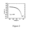
- a common approach to estimate the band-gap of a ⁇ -conjugated material is to measure the optical absorption and calculate the energy at the longest wavelength onset. It is generally believed that, in order for BHJ solar cells to be commercially viable, they must achieve high V oc (> ⁇ 0.7 V), high FF (> ⁇ 65%), and an optimized J sc . It has been shown that J sc is optimally satisfied by absorbers having a band gap ⁇ ⁇ 1.6 eV.
- V oc - E HOMO donor - E LUMO acceptor + 0.4 / e
- E HOMO , E LUMO , and e are the Highest Occupied Molecular Orbital (HOMO) energy (or HOMO level), the Lowest Unoccupied Molecular Orbital (LUMO) energy (or LUMO level), and the electron charge, respectively.
- the LUMO level of PCBM is about -4.3 eV.
- the V oc of a solar cell therefore, also can be used to estimate the HOMO level of the donor material (given the known LUMO level of PCBM).
- the HOMO level of the donor material often determines its air stability.
- state-of-the-art P3HT/PCBM BHJ solar cells typically have a V oc of about 0.6 V, suggesting that the HOMO level of P3HT is ⁇ -5.3 eV.
- P3HT has poor air stability.
- a donor material having a lower HOMO value than P3HT i.e., ⁇ -5.4 eV or lower
- a donor material with a lower HOMO level also will likely increase the V oc of a solar cell, and in turn, its efficiency.
- State-of-the-art BHJ solar cells exhibit a PCE of ⁇ 4-5%.
- the band-gap of P3HT is ⁇ 2.0 eV, and it can absorb only a small portion (30%) of the solar spectrum. It is important to develop a donor material with a band-gap of about 1.6 eV or smaller so that a larger portion of the solar spectrum can be utilized.
- the donor material needs to have an absorption onset at ⁇ 800 nm or larger (the absorption onset of a material is equal to 1240 nm divided by its band-gap) to match the peak intensity region (700-800 nm) of the solar spectrum.
- low band-gap ( ⁇ ⁇ 1.6 eV) donor materials to replace P3HT in BHJ solar cells.
- low band-gap donor-based BHJ solar cells Although there have been a few reports of low band-gap donor-based BHJ solar cells, none of these solar cells showed much performance improvement over P3HT/PCBM-based solar cells.
- the BHJ solar cells based on these new donor materials typically exhibit poor fill factor ( ⁇ 60%).
- the present teachings provide certain oligomeric and polymeric compounds that can be used as organic semiconductors. Also provided are associated devices and related methods for the preparation and use of these compounds.
- the present compounds can exhibit properties such as excellent charge transport characteristics in ambient conditions, optimized optical absorption, chemical stability, low-temperature processability, large solubility in common solvents, and processing versatility (e.g., via various solution processes).
- optoelectronic devices such as solar cells that incorporate one or more of the present compounds as a photoactive layer can exhibit high performance in ambient conditions, for example, demonstrating one or more of low band-gap, high fill factor, high open circuit voltage, and high power conversion efficiency, and preferably all of these criteria.
- other organic semiconductor-based devices such as OLETs can be fabricated efficiently using the organic semiconductor materials described herein.
- the present teachings also provide methods of preparing such compounds and semiconductor materials, as well as various compositions, composites, and devices that incorporate the compounds and semiconductor materials disclosed herein.
- the present teachings provide organic semiconductor materials that are prepared from various ⁇ -conjugated oligomeric and polymeric compounds having typically an electron-rich repeat unit and an electron-poor repeat unit.
- Compounds of the present teachings can exhibit semiconductor behavior such as high carrier mobility and/or good current modulation characteristics in a field-effect device, optimized light absorption/charge separation in a photovoltaic device, and/or charge transport/recombination/light emission in a light-emitting device.
- the present compounds can possess certain processing advantages such as solution-processability and/or good stability (e.g., air stability) in ambient conditions.
- the compounds of the present teachings can be used to prepare either p-type (donor or hole-transporting), n-type (acceptor or electron-transporting), or ambipolar semiconductor materials, which in turn can be used to fabricate various organic or hybrid optoelectronic articles, structures and devices, including organic photovoltaic devices and organic light-emitting transistors.
- an "oligomeric compound” or “oligomer” or a “polymeric compound” (or “polymer”) refers to a molecule including a plurality of one or more repeat units connected by covalent chemical bonds.
- An oligomeric or polymeric compound can be represented by the general formula: wherein M is the repeat unit or monomer.
- the degree of polymerization can range from 2 to greater than 10,000. For example, for oligomeric compounds, the degree of polymerization can range from 2 to 9; and for polymeric compounds, the degree of polymerization can range from 10 to about 10,000.
- the oligomeric or polymeric compound can have only one type of repeat unit as well as two or more types of different repeat units.
- a polymeric compound When a polymeric compound has only one type of repeat unit, it can be referred to as a homopolymer. When a polymeric compound has two or more types of different repeat units, the term "copolymer” or “copolymeric compound” can be used instead.
- the oligomeric or polymeric compound can be linear or branched. Branched polymers can include dendritic polymers, such as dendronized polymers, hyperbranched polymers, and brush polymers (also called bottle-brushes). Unless specified otherwise, the assembly of the repeat units in the copolymer can be head-to-tail, head-to-head, or tail-to-tail.
- the copolymer can be a random copolymer, an alternating copolymer, or a block copolymer.
- the general formula: can be used to represent a co-oligomer or copolymer of A and B having x mole fraction of A and y mole fraction of B in the copolymer, where the manner in which comonomers A and B is repeated can be alternating, random, regiorandom, regioregular, or in blocks.
- the degree of polymerization (n) can range from 2 to greater than 10,000.
- a "cyclic moiety" can include one or more (e.g., 1-6) carbocyclic or heterocyclic rings.
- the cyclic moiety can be a cycloalkyl group, a heterocycloalkyl group, an aryl group, or a heteroaryl group (i.e., can include only saturated bonds, or can include one or more unsaturated bonds regardless of aromaticity), each including, for example, 3-24 ring atoms and optionally can be substituted as described herein.
- the cyclic moiety is a "monocyclic moiety”
- the "monocyclic moiety" can include a 3-14 membered aromatic or non-aromatic, carbocyclic or heterocyclic ring.
- a monocyclic moiety can include, for example, a phenyl group or a 5-or 6-membered heteroaryl group, each of which optionally can be substituted as described herein.
- the cyclic moiety is a "polycyclic moiety”
- the "polycyclic moiety” can include two or more rings fused to each other (i.e., sharing a common bond) and/or connected to each other via a spiro atom, or one or more bridged atoms.
- a polycyclic moiety can include an 8-24 membered aromatic or non-aromatic, carbocyclic or heterocyclic ring, such as a C 8-24 aryl group or an 8-24 membered heteroaryl group, each of which optionally can be substituted as described herein.
- halo or halogen refers to fluoro, chloro, bromo, and iodo.
- alkyl refers to a straight-chain or branched saturated hydrocarbon group.
- alkyl groups include methyl (Me), ethyl (Et), propyl (e.g., n -propyl and iso -propyl), butyl (e.g., n -butyl, iso -butyl, sec -butyl, tert -butyl), pentyl groups (e.g., n -pentyl, iso -pentyl, neo -pentyl), and hexyl groups.
- an alkyl group can have 1 to 40 carbon atoms (i.e., C 1-40 alkyl group), for example, 1-20 carbon atoms (i.e., C 1-20 alkyl group).
- an alkyl group can have 1 to 6 carbon atoms, and can be referred to as a "lower alkyl group.” Examples of lower alkyl groups include methyl, ethyl, propyl (e.g., n -propyl and iso- propyl), and butyl groups (e.g., n -butyl, iso -butyl, sec -butyl, tert -butyl) .
- alkyl groups can be substituted as described herein.
- An alkyl group is generally not substituted with another alkyl group, an alkenyl group, or an alkynyl group.
- haloalkyl refers to an alkyl group having one or more halogen substituents.
- a haloalkyl group can have 1 to 40 carbon atoms (i.e., C 1-40 haloalkyl group), for example, 1 to 20 carbon atoms (i.e., C 1-20 haloalkyl group).
- Examples of haloalkyl groups include CF 3 , C 2 F 5 , CHF 2 , CH 2 F, CCl 3 , CHCl 2 , CH 2 Cl, and C 2 Cl 5 .
- Perhaloalkyl groups i.e., alkyl groups where all of the hydrogen atoms are replaced with halogen atoms (e.g., CF 3 and C 2 F 5 ), are included within the definition of "haloalkyl.”
- a C 1-40 haloalkyl group can have the formula-C s H 2s+1-t X 0 t , where X 0 , at each occurrence, is F, Cl, Br or I, s is an integer in the range of 1 to 40, and t is an integer in the range of 1 to 81, provided that t is less than or equal to 2s+1.
- Haloalkyl groups that are not perhaloalkyl groups can be substituted as described herein.
- alkoxy refers to -O-alkyl group.
- alkoxy groups include, but are not limited to, methoxy, ethoxy, propoxy (e.g., n-propoxy and isopropoxy), t -butoxy, pentoxyl, and hexoxyl groups.
- the alkyl group in the -O-alkyl group can be substituted as described herein.
- alkylthio refers to an -S-alkyl group (which, in some cases, can be expressed as -S(O) w -alkyl, wherein w is 0).
- alkylthio groups include, but are not limited to, methylthio, ethylthio, propylthio (e.g., n-propylthio and isopropylthio), t -butylthio, pentylthio, and hexylthio groups.
- the alkyl group in the -S-alkyl group can be substituted as described herein.
- arylalkyl refers to an -alkyl-aryl group, where the arylalkyl group is covalently linked to the defined chemical structure via the alkyl group.
- An arylalkyl group is within the definition of a -Y-C 6-14 aryl group, where Y is as defined herein.
- An example of an arylalkyl group is a benzyl group (-CH 2 -C 6 H 5 ).
- An arylalkyl group optionally can be substituted, i.e., the aryl group and/or the alkyl group, can be substituted as disclosed herein.
- alkenyl refers to a straight-chain or branched alkyl group having one or more carbon-carbon double bonds.
- alkenyl groups include ethenyl, propenyl, butenyl, pentenyl, hexenyl, butadienyl, pentadienyl, and hexadienyl groups.
- the one or more carbon-carbon double bonds can be internal (such as in 2-butene) or terminal (such as in 1-butene).
- an alkenyl group can have 2 to 40 carbon atoms (i.e., C 2-40 alkenyl group), for example, 2 to 20 carbon atoms (i.e., C 2-20 alkenyl group).
- alkenyl groups can be substituted as described herein.
- An alkenyl group is generally not substituted with another alkenyl group, an alkyl group, or an alkynyl group.
- alkynyl refers to a straight-chain or branched alkyl group having one or more triple carbon-carbon bonds.
- alkynyl groups include ethynyl, propynyl, butynyl, pentynyl, and hexynyl.
- the one or more triple carbon-carbon bonds can be internal (such as in 2-butyne) or terminal (such as in 1-butyne).
- an alkynyl group can have 2 to 40 carbon atoms (i.e., C 2-40 alkynyl group), for example, 2 to 20 carbon atoms (i.e., C 2-20 alkynyl group).
- alkynyl groups can be substituted as described herein.
- An alkynyl group is generally not substituted with another alkynyl group, an alkyl group, or an alkenyl group.
- cycloalkyl refers to a non-aromatic carbocyclic group including cyclized alkyl, alkenyl, and alkynyl groups.
- a cycloalkyl group can have 3 to 24 carbon atoms, for example, 3 to 20 carbon atoms (e.g., C 3-14 cycloalkyl group).
- a cycloalkyl group can be monocyclic (e.g., cyclohexyl) or polycyclic (e.g., containing fused, bridged, and/or spiro ring systems), where the carbon atoms are located inside or outside of the ring system.
- cycloalkyl groups include cyclopropyl, cyclobutyl, cyclopentyl, cyclohexyl, cycloheptyl, cyclopentenyl, cyclohexenyl, cyclohexadienyl, cycloheptatrienyl, norbornyl, norpinyl, norcaryl, adamantyl, and spiro[4.5]decanyl groups, as well as their homologs and isomers.
- cycloalkyl groups can be substituted as described herein.
- heteroatom refers to an atom of any element other than carbon or hydrogen and includes, for example, nitrogen, oxygen, silicon, sulfur, phosphorus, and selenium.
- cycloheteroalkyl refers to a non-aromatic cycloalkyl group that contains at least one ring heteroatom selected from O, S, Se, N, P, and Si (e.g., O, S, and N), and optionally contains one or more double or triple bonds.
- a cycloheteroalkyl group can have 3 to 24 ring atoms, for example, 3 to 20 ring atoms (e.g., 3-14 membered cycloheteroalkyl group).
- N, P, S, or Se atoms in a cycloheteroalkyl ring may be oxidized (e.g., morpholine N-oxide, thiomorpholine S-oxide, thiomorpholine S,S-dioxide).
- nitrogen or phosphorus atoms of cycloheteroalkyl groups can bear a substituent, for example, a hydrogen atom, an alkyl group, or other substituents as described herein.
- Cycloheteroalkyl groups can also contain one or more oxo groups, such as oxopiperidyl, oxooxazolidyl, dioxo-(1H,3H)-pyrimidyl, and oxo-2(1H)-pyridyl.
- oxo groups such as oxopiperidyl, oxooxazolidyl, dioxo-(1H,3H)-pyrimidyl, and oxo-2(1H)-pyridyl.
- cycloheteroalkyl groups include, among others, morpholinyl, thiomorpholinyl, pyranyl, imidazolidinyl, imidazolinyl, oxazolidinyl, pyrazolidinyl, pyrazolinyl, pyrrolidinyl, pyrrolinyl, tetrahydrofuranyl, tetrahydrothiophenyl, piperidinyl, and piperazinyl.
- cycloheteroalkyl groups can be substituted as described herein.
- aryl refers to an aromatic monocyclic hydrocarbon ring system or a polycyclic ring system in which two or more aromatic hydrocarbon rings are fused (i.e., having a bond in common with) together or at least one aromatic monocyclic hydrocarbon ring is fused to one or more cycloalkyl and/or cycloheteroalkyl rings.
- An aryl group can have 6 to 24 carbon atoms in its ring system (e.g., C 6-20 aryl group), which can include multiple fused rings.
- a polycyclic aryl group can have 8 to 24 carbon atoms. Any suitable ring position of the aryl group can be covalently linked to the defined chemical structure.
- aryl groups having only aromatic carbocyclic ring(s) include phenyl, 1-naphthyl (bicyclic), 2-naphthyl (bicyclic), anthracenyl (tricyclic), phenanthrenyl (tricyclic), and pentacenyl (pentacyclic) groups.
- polycyclic ring systems in which at least one aromatic carbocyclic ring is fused to one or more cycloalkyl and/or cycloheteroalkyl rings include, among others, benzo derivatives of cyclopentane (i.e., an indanyl group, which is a 5,6-bicyclic cycloalkyl/aromatic ring system), cyclohexane (i.e., a tetrahydronaphthyl group, which is a 6,6-bicyclic cycloalkyl/aromatic ring system), imidazoline (i.e., a benzimidazolinyl group, which is a 5,6-bicyclic cycloheteroalkyl/aromatic ring system), and pyran (i.e., a chromenyl group, which is a 6,6-bicyclic cycloheteroalkyl/aromatic ring system).
- aryl groups include benzodioxanyl, benzodioxolyl, chromanyl, and indolinyl groups.
- aryl groups can be substituted as described herein.
- an aryl group can have one or more halogen substituents, and can be referred to as a "haloaryl" group.
- Perhaloaryl groups i.e., aryl groups where all of the hydrogen atoms are replaced with halogen atoms (e.g., -C 6 F 5 ), are included within the definition of "haloaryl.”
- an aryl group is substituted with another aryl group and can be referred to as a biaryl group. Each of the aryl groups in the biaryl group can be substituted as disclosed herein.
- heteroaryl refers to an aromatic monocyclic ring system containing at least one ring heteroatom selected from oxygen (O), nitrogen (N), sulfur (S), silicon (Si), and selenium (Se) or a polycyclic ring system where at least one of the rings present in the ring system is aromatic and contains at least one ring heteroatom.
- Polycyclic heteroaryl groups include those having two or more heteroaryl rings fused together, as well as those having at least one monocyclic heteroaryl ring fused to one or more aromatic carbocyclic rings, non-aromatic carbocyclic rings, and/or non-aromatic cycloheteroalkyl rings.
- a heteroaryl group as a whole, can have, for example, 5 to 24 ring atoms and contain 1-5 ring heteroatoms (i.e., 5-20 membered heteroaryl group).
- the heteroaryl group can be attached to the defined chemical structure at any heteroatom or carbon atom that results in a stable structure.
- heteroaryl rings do not contain O-O, S-S, or S-O bonds.
- one or more N or S atoms in a heteroaryl group can be oxidized (e.g., pyridine N-oxide, thiophene S-oxide, thiophene S,S-dioxide).
- heteroaryl groups include, for example, the 5- or 6-membered monocyclic and 5-6 bicyclic ring systems shown below: where T is O, S, NH, N-alkyl, N-aryl, N-(arylalkyl) (e.g., N-benzyl), SiH 2 , SiH(alkyl), Si(alkyl) 2 , SiH(arylalkyl), Si(arylalkyl) 2 , or Si(alkyl)(arylalkyl).
- T is O, S, NH, N-alkyl, N-aryl, N-(arylalkyl) (e.g., N-benzyl), SiH 2 , SiH(alkyl), Si(alkyl) 2 , SiH(arylalkyl), Si(arylalkyl) 2 , or Si(alkyl)(arylalkyl).
- heteroaryl rings examples include pyrrolyl, furyl, thienyl, pyridyl, pyrimidyl, pyridazinyl, pyrazinyl, triazolyl, tetrazolyl, pyrazolyl, imidazolyl, isothiazolyl, thiazolyl, thiadiazolyl, isoxazolyl, oxazolyl, oxadiazolyl, indolyl, isoindolyl, benzofuryl, benzothienyl, quinolyl, 2-methylquinolyl, isoquinolyl, quinoxalyl, quinazolyl, benzotriazolyl, benzimidazolyl, benzothiazolyl, benzisothiazolyl, benzisoxazolyl, benzoxadiazolyl, benzoxazolyl, cinnolinyl, 1H-indazolyl, 2H-indazolyl
- heteroaryl groups include 4,5,6,7-tetrahydroindolyl, tetrahydroquinolinyl, benzothienopyridinyl, and benzofuropyridinyl groups.
- heteroaryl groups can be substituted as described herein.
- compounds of the present teachings can include a "divalent group" defined herein as a linking group capable of forming a covalent bond with two other moieties.
- compounds of the present teachings can include a divalent C 1-20 alkyl group (e.g., a methylene group), a divalent C 2-20 alkenyl group (e.g., a vinylyl group), a divalent C 2-20 alkynyl group (e.g., an ethynylyl group).
- a divalent C 6-14 aryl group e.g., a phenylyl group
- a divalent 3-14 membered cycloheteroalkyl group e.g., a pyrrolidylyl
- a divalent 5-14 membered heteroaryl group e.g., a thienylyl group
- a chemical group e.g., -Ar-
- -Ar- is understood to be divalent by the inclusion of the two bonds before and after the group.
- an “electron-withdrawing group” (“EWG”) or an “electron-accepting group” or an “electron-acceptor” refers to a functional group that draws electrons to itself more than a hydrogen atom would if it occupied the same position in a molecule.
- electron-withdrawing groups include, but are not limited to, halogen or halo (e.g., F, Cl, Br, I), -NO 2 , -CN, -NC, -S(R 0 ) 2 + , -N(R 0 ) 3 + , -SO 3 H, -SO 2 R 0 , -SO 3 R 0 , -SO 2 NHR 0 , -SO 2 N(R 0 ) 2 , -COOH, -COR 0 , -COOR 0 , -CONHR 0 , -CON(R 0 ) 2 , C 1-40 haloalkyl groups, C 6-14 aryl groups, and 5-14 membered electron-poor heteroaryl groups; where R 0 is a C 1-20 alkyl group, a C 2-20 alkenyl group, a C 2-20 alkynyl group, a C 1-20 haloalkyl group, a C 1-20
- each of the C 1-20 alkyl group, the C 2- 20 alkenyl group, the C 2-20 alkynyl group, the C 1-20 haloalkyl group, the C 1-20 alkoxy group, the C 6-14 aryl group, the C 3-14 cycloalkyl group, the 3-14 membered cycloheteroalkyl group, and the 5-14 membered heteroaryl group optionally can be substituted with 1-5 small electron-withdrawing groups such as F, Cl, Br, -NO 2 , -CN, NC,-S(R 0 ) 2 +,-N(R 0 ) 3 + , -SO 3 H, -SO 2 R 0 , -SO 3 R 0 , -SO 2 NHR 0 , -SO 2 N(R 0 ) 2 , -COOH, -COR 0 , -COOR 0 ,-CONHR 0 , and -CON(R 0 ) 2 .
- an “electron-donating group” can be used synonymously herein with “electron donor”.
- an “electron-donating group” or an “electron-donor” refers to a functional group that donates electrons to a neighboring atom more than a hydrogen atom would if it occupied the same position in a molecule.
- electron-donating groups include -OH, -OR 0 , -NH 2 , -NHR 0 , -N(R 0 ) 2 , and 5-14 membered electron-rich heteroaryl groups, where R 0 is a C 1-20 alkyl group, a C 2-20 alkenyl group, a C 2-20 alkynyl group, a C 6-14 aryl group, or a C 3-14 cycloalkyl group.
- Various unsubstituted heteroaryl groups can be described as electron-rich (or ⁇ -excessive) or electron-poor (or ⁇ -deficient). Such classification is based on the average electron density on each ring atom as compared to that of a carbon atom in benzene.
- electron-rich systems include 5-membered heteroaryl groups having one heteroatom such as furan, pyrrole, and thiophene; and their benzofused counterparts such as benzofuran, benzopyrrole, and benzothiophene.
- Examples of electron-poor systems include 6-membered heteroaryl groups having one or more heteroatoms such as pyridine, pyrazine, pyridazine, and pyrimidine; as well as their benzofused counterparts such as quinoline, isoquinoline, quinoxaline, cinnoline, phthalazine, naphthyridine, quinazoline, phenanthridine, acridine, and purine.
- Mixed heteroaromatic rings can belong to either class depending on the type, number, and position of the one or more heteroatom(s) in the ring. See Katritzky, A.R and Lagowski, J.M., Heterocyclic Chemistry (John Wiley & Sons, New York, 1960 ).
- C 1-6 alkyl is specifically intended to individually disclose C 1 , C 2 , C 3 , C 4 , C 5 , C 6 , C 1 -C 6 , C 1 -C 5 , C 1 -C 4 , C 1 -C 3 , C 1 -C 2 , C 2 -C 6 , C 2 -C 5 , C 2 -C 4 , C 2 -C 3 , C 3 -C 6 , C 3 -C 5 , C 3 -C 4 , C 4 -C 6 , C 4 -C 5 , and C 5 -C 6 alkyl.
- an integer in the range of 0 to 40 is specifically intended to individually disclose 0, 1, 2, 3, 4, 5, 6, 7, 8, 9, 10, 11, 12, 13, 14, 15, 16, 17, 18, 19, 20, 21, 22, 23, 24, 25, 26, 27, 28, 29, 30, 31, 32, 33, 34, 35, 36, 37, 38, 39, and 40, and an integer in the range of 1 to 20 is specifically intended to individually disclose 1, 2, 3, 4, 5, 6, 7, 8, 9, 10, 11, 12, 13, 14, 15, 16, 17, 18, 19, and 20.
- phrases "optionally substituted with 1-5 substituents” is specifically intended to individually disclose a chemical group that can include 0, 1,2, 3, 4, 5, 0-5, 0-4, 0-3, 0-2, 0-1, 1-5, 1-4, 1-3, 1-2, 2-5, 2-4, 2-3, 3-5, 3-4, and 4-5 substituents.
- asymmetric atom also referred as a chiral center
- some of the compounds can contain two or more asymmetric atoms or centers, which can thus give rise to optical isomers (enantiomers) and diastereomers (geometric isomers).
- the present teachings include such optical isomers and diastereomers, including their respective resolved enantiomerically or diastereomerically pure isomers (e.g., (+) or (-) stereoisomer) and their racemic mixtures, as well as other mixtures of the enantiomers and diastereomers.
- optical isomers can be obtained in enantiomerically enriched or pure form by standard procedures known to those skilled in the art, which include, for example, chiral separation, diastereomeric salt formation, kinetic resolution, and asymmetric synthesis.
- the present teachings also encompass cis- and trans-isomers of compounds containing alkenyl moieties (e.g., alkenes, azo, and imines). It also should be understood that the compounds of the present teachings encompass all possible regioisomers in pure form and mixtures thereof.
- the preparation of the present compounds can include separating such isomers using standard separation procedures known to those skilled in the art, for example, by using one or more of column chromatography, thin-layer chromatography, simulated moving-bed chromatography, and high-performance liquid chromatography.
- column chromatography thin-layer chromatography
- simulated moving-bed chromatography simulated moving-bed chromatography
- high-performance liquid chromatography mixtures of regioisomers can be used similarly to the uses of each individual regioisomer of the present teachings as described herein and/or known by a skilled artisan.
- LG refers to a charged or uncharged atom (or group of atoms) that can be displaced as a stable species as a result of, for example, a substitution or elimination reaction.
- leaving groups include, but are not limited to, halogen (e.g., Cl, Br, I), azide (N 3 ), thiocyanate (SCN), nitro (NO 2 ), cyanate (CN), water (H 2 O), ammonia (NH 3 ), and sulfonate groups (e.g., OSO 2 -R, wherein R can be a C 1-10 alkyl group or a C 6-14 aryl group each optionally substituted with 1-4 groups independently selected from a C 1-10 alkyl group and an electron-withdrawing group) such as tosylate (toluenesulfonate, OTs), mesylate (methanesulfonate, OMs), brosylate (p-bro
- a "p-type semiconductor material” or a “donor” material refers to a semiconductor material having holes as the majority current or charge carriers.
- a p-type semiconductor material when deposited on a substrate, it can provide a hole mobility in excess of about 10 -5 cm 2 /Vs.
- a p-type semiconductor in the case of field-effect devices, can also exhibit a current on/off ratio of greater than about 10.
- an "n-type semiconductor material” or an “acceptor” material refers to a semiconductor material having electrons as the majority current or charge carriers.
- an n-type semiconductor material when deposited on a substrate, it can provide an electron mobility in excess of about 10 -5 cm 2 /Vs.
- an n-type semiconductor can also exhibit a current on/off ratio of greater than about 10.
- mobility refers to a measure of the velocity with which charge carriers, for example, holes (or units of positive charge) in the case of a p-type semiconductor material and electrons in the case of an n-type semiconductor material, move through the material under the influence of an electric field. This parameter, which depends on the device architecture, can be measured using a field-effect device or space-charge limited current measurements.
- Fill factor is a key parameter in evaluating the performance of solar cells. Commercial solar cells typically have a fill factor of about 0.60% or greater.
- V oc the open-circuit voltage
- the power conversion efficiency (PCE) of a solar cell is the percentage of power converted from absorbed light to electrical energy.
- the PCE of a solar cell can be calculated by dividing the maximum power point (P m ) by the input light irradiance (E, in W/m 2 ) under standard test conditions (STC) and the surface area of the solar cell (A c in m 2 ).
- STC typically refers to a temperature of 25°C and an irradiance of 1000 W/m 2 with an air mass 1.5 (AM 1.5) spectrum.
- a component such as a thin film layer
- a component can be considered "photoactive" if it contains one or more compounds that can absorb photons to produce excitons for the generation of a photocurrent.
- a compound can be considered “ambient stable” or “stable at ambient conditions” when a transistor incorporating the compound as its semiconducting material exhibits a carrier mobility that is maintained at about its initial measurement when the compound is exposed to ambient conditions, for example, air, ambient temperature, and humidity, over a period of time.
- ambient stable if a transistor incorporating the compound shows a carrier mobility that does not vary more than 20% or more than 10% from its initial value after exposure to ambient conditions, including, air, humidity and temperature, over a 3 day, 5 day, or 10 day period.
- solution-processable refers to compounds (e.g., polymers), materials, or compositions that can be used in various solution-phase processes including spin-coating, printing (e.g., inkjet printing, screen printing, pad printing, offset printing, gravure printing, flexographic printing, lithographic printing, and mass-printing), spray coating, electrospray coating, drop casting, dip coating, and blade coating.
- printing e.g., inkjet printing, screen printing, pad printing, offset printing, gravure printing, flexographic printing, lithographic printing, and mass-printing
- spray coating e.g., electrospray coating, drop casting, dip coating, and blade coating.
- the present teachings relate to certain oligomeric and polymeric compounds that can be used as organic semiconductors.
- the present compounds can have good solubility in various common solvents and good stability in air.
- optical or optoelectronic devices including, but not limited to, photovoltaic or solar cells, light emitting diodes, and light emitting transistors
- the present compounds can confer various desirable performance properties.
- the solar cell can exhibit very high power conversion efficiency (e.g., about 4.0% or greater), fill factor (e.g., about 60% or greater), and/or open circuit voltage (e.g., about 0.7 V or greater).
- the present compounds also can be processed into very efficient solar cells without a thermally annealing step, thus providing time- and cost-saving benefits and allowing a larger variety of materials to be used in various components of the solar cell.
- the present teachings provide various conjugated oligomeric and polymeric compounds, where each compound includes at least two different monomeric units.
- the present compounds can be represented by the formula: where A and B are different and can be repeated in a random or alternating manner; x and y represent the mole fractions of A and B, respectively, where 0.1 ⁇ x ⁇ 0.9, 0.1 ⁇ y ⁇ 0.9, and the sum of x and y is about 1; and n represents a degree of polymerization in the range from 2 to about 10,000 or greater.
- the present compounds can be represented by the formula: where A' and A" have the definition of A as described above, B' and B" have the definitions of B as described above, provided that A' and A" and/or B' and B" differ from each other in terms of substitution; x and y represent mole fractions, where 0.1 ⁇ x ⁇ 0.9, 0.1 ⁇ y ⁇ 0.9, and the sum of x and y is about 1; and n represents a degree of polymerization in the range from 2 to about 10,000 or greater.
- one of A' and A" can be substituted with one or more solubilizing groups while the other is unsubstituted.
- one or more moieties in B' can be substituted while the same moieties in B are unsubstituted.
- the unit comprising x mole fraction of the compound and the unit comprising y mole fraction of the compound, i.e., the units can be repeated in a random manner.
- the repeat unit A, A', or A" can include a conjugated polycyclic moiety of the formula: wherein X is N or CR 3 and Y is N or CR 4 , i.e., an optionally substituted benzodithienyl moiety of the formula: or an optionally substituted benzodithiazolyl moiety of the formula: where R 1 , R 2 , R 3 , and R 4 independently can be H or a substituent which can impart improved desirable properties to the compound as a whole.
- certain substituents including one or more electron-withdrawing or electron-donating moieties can modulate the electronic properties of the compound, while substituents that include one or more aliphatic chains can improve the solubility of the compound in organic solvents.
- each of R 1 , R 2 , R 3 , and R 4 independently can be selected from H, a halogen, CN, OR', SR', C(O)R', C(O)OR', SO 2 R', a C 1-10 alkyl group, a C 2-40 alkenyl group, a C 2-40 alkynyl group, a C 1-10 haloalkyl group, a -L-C 3-10 cycloalkyl group, a -L'-C 6-14 aryl group, a -L'-C 6-14 haloaryl group, a -L'-3-12 membered cycloheteroalkyl group, and a -L'-5-14 membered heteroaryl group; wherein:
- At least one of R 1 , R 2 , R 3 , and R 4 independently can be a small functional group such as a halogen, CN, OR', C(O)R', C(O)OR', or SO 2 R', where R' can be H or a lower alkyl group.
- At least one of R 1 , R 2 , R 3 , and R 4 independently can be a linear or branched C 3-40 alkyl group, examples of which include an n-hexyl group, an n-octyl group, an n-dodecyl group, a 1-methylpropyl group, a 1-methylbutyl group, a 1-methylpentyl group, a 1-methylhexyl group, a 1-ethylpropyl group, a 1-ethylbutyl group, a 1,3-dimethylbutyl group, a 2-ethylhexyl group, a 2-hexyloctyl group, a 2-octyldodecyl group, and a 2-decyltetradecyl group.
- At least one of R 1 , R 2 , R 3 , and R 4 independently can be a linear or branched C 3-40 alkenyl group (such as the linear or branched C 3-40 alkyl groups specified above but with one or more saturated bonds replaced by unsaturated bonds).
- at least one of R 1 , R 2 , R 3 , and R 4 independently can be a branched C 3-20 alkyl group or a branched C 3-20 alkenyl group.
- At least one of R 1 , R 2 , R 3 , and R 4 independently can be a linear or branched C 6-40 alkyl or alkenyl group, an arylalkyl group (e.g., a benzyl group) substituted with a linear or branched C 6-40 alkyl or alkenyl group, an aryl group (e.g., a phenyl group) substituted with a linear or branched C 6-40 alkyl or alkenyl group, or a biaryl group (e.g., a biphenyl group) substituted with a linear or branched C 6-40 alkyl or alkenyl group, wherein each of these groups optionally can be substituted with 1-5 halo groups (e.g., F).
- arylalkyl group e.g., a benzyl group
- an aryl group e.g., a phenyl group substituted with a linear or branched C 6
- At least one of R 1 , R 2 , R 3 , and R 4 independently can be a biaryl group wherein the two aryl groups are covalently linked via a linker.
- the linker can be a divalent C 1-40 alkyl group wherein one or more non-adjacent CH 2 groups optionally can be replaced by -O-, -S-, or -Se-, i.e., O, S, and/or Se atoms are not linked directly to one another.
- the linker can include other heteroatoms and/or functional groups as described herein.
- R 1 , R 2 , R 3 , and R 4 independently can be selected from H or -L'-R a , where R a is selected from a C 1-40 alkyl group, a C 2-40 alkenyl group, a C 2-40 alkynyl group, and a C 1-40 haloalkyl group, each of which optionally can be substituted with 1-10 substituents independently selected from a halogen, -CN, NO 2 , OH, -NH 2 , -NH(C 1-20 alkyl), -N(C 1-20 alkyl) 2 , -S(O) 2 OH, -CHO, -C(O)-C 1-20 alkyl, -C(O)OH, -C(O)-OC 1-20 alkyl, -C(O)NH 2 , -C(O)NH-C 1-20 alkyl, -C(O)N(C 1-20 alkyl) 2 ,
- L' can be a linker selected from -Y-O-Y-, -Y-[S(O) w ]-Y-, -Y-C(O)-Y-, -Y-[NR c C(O)]-Y-, -Y-[C(O)NR c ]-, -Y-NR c -Y-, -Y-[SiR c 2 ]-Y-, where Y, at each occurrence, independently is selected from a divalent C 1-20 alkyl group, a divalent C 2-20 alkenyl group, a divalent C 2-20 haloalkyl group, and a covalent bond; R c is selected from H, a C 1-6 alkyl group, a C 6-14 aryl group, and a -C 1-6 alkyl-C 6-14 aryl group; and w is 0, 1, or 2.
- R 1 , R 2 , R 3 , and R 4 independently can be selected from H, a C 3-40 alkyl group, an -O-C 3-40 alkyl group, an -S-C 3-40 alkyl group, a C 4-40 alkenyl group, a C 4-40 alkynyl group, and a C 3-40 haloalkyl group, where each of these groups can be linear or branched, and optionally can be substituted as described herein.
- one or more of R 1 , R 2 , R 3 , and R 4 independently can include one or more cyclic moieties.
- the conjugated polycyclic moiety can be symmetrically substituted, that is, R 1 and R 2 can be identical groups, and/or when X and Y are CR 3 and CR 4 , respectively, R 3 and R 4 can be identical groups.
- R 1 and R 2 and/or each of R 3 and R 4 can be a branched C 3-40 alkyl group, a branched C 3-40 haloalkyl group, a branched C 3-40 alkoxy group, or a branched C 3-40 alkylthio group.
- the repeat unit B, B', or B" in the present oligomeric or polymeric compounds can have the formula: -(Ar)-M-(Ar)- where each Ar can be an optionally substituted 5-10 membered aryl or heteroaryl group; and M can be an optionally substituted benzofused heteroaryl moiety as described herein.
- the optionally substituted benzofused heteroaryl moiety can be represented by the formula: wherein Het, at each occurrence, is a monocyclic moiety including at least one heteroatom in its ring, and R 5 and R 6 independently can be H or -L-R, where L and R are as defined herein.
- M can be selected from: wherein R 8 is H or a C 1-40 alkyl group, and R 5 and R 6 are as defined herein.
- M can be selected from: wherein R 5 and R 6 are as defined herein.
- R 5 and R 6 can be H or a C 1-40 alkyl group.
- copolymers according to the present teachings can be represented by Formula II: wherein R 1 , R 2 , R 5 , R 6 , R 7 , Z, x and y are as defined herein.
- R 5 and R 6 independently can be H or a C 1-10 alkyl group; and each R 7 can be a C 1-40 alkyl group or a C 1-40 alkoxy group.
- certain copolymers according to the present teachings can be represented by Formula III: wherein R 1 , R 2 , R 3 , R 4 , R 5 , R 6 , R 7 , x and y are as defined herein.
- R 5 and R 6 independently can be H or a C 1-40 alkyl group; and each R 7 can be a C 1-40 alkyl group or a C 1-40 alkoxy group.
- compounds of formula III can be represented by a formula selected from: and wherein R 1 , R 2 , R 3 , R 4 , R 7 , x and y are as defined herein.
- R 3 and R 4 can be H, and R 1 and R 2 can be -L-R, wherein L and R are as defined herein.
- R 1 and R 2 can be H, and R 3 and R 4 can be -L-R, wherein L and R are as defined herein.
- -L-R can be selected from a C 3-40 alkyl group (R), a C 3-40 alkoxy group (-O-R), and a C 3-40 alkylthio group (-S-R).
- copolymers of the present teachings can be represented by formula IV: including a formula selected from: and wherein R is a C 1-40 alkyl group, and R 7 , x and y are as defined herein.
- R can be a branched C 6-20 alkyl group
- R 7 can be a linear C 6-20 alkyl group.
- R can be a branched C 6-20 alkyl group
- R 7 can be a linear C 6-20 alkoxy group.
- the mole fractions x and y can range between about 0.2 and about 0.8, i.e., 0.2 ⁇ x ⁇ 0.8 and 0.2 ⁇ y ⁇ 0.8, provided that the sum of x and y is about 1.
- copolymers of formula IV can be represented by a formula selected from: and wherein R, at each occurrence, independently can be a C 6-20 alkyl group, and x and y are as defined herein.
- copolymers of the present teachings can be represented by formula V: including a formula selected from: and wherein R is a C 1-40 alkyl group, and R 7 , x and y are as defined herein.
- R can be a branched C 6-20 alkyl group
- R 7 can be a linear C 6-20 alkyl group.
- R can be a branched C 6-20 alkyl group
- R 7 can be a linear C 6-20 alkoxy group.
- the mole fractions x and y can range between about 0.2 and about 0.8, i.e., 0.2 ⁇ x ⁇ 0.8 and 0.2 ⁇ y ⁇ 0.8, provided that the sum of x and y is about 1.
- copolymers of formula V can be represented by a formula selected from: and wherein R, at each occurrence, independently can be a C 6-20 alkyl group, and x and y are as defined herein.
- the optionally substituted benzodithienyl or benzodithiazolyl groups in formula I can be replaced by another optionally substituted conjugated polycyclic moiety [ ⁇ -2], where [ ⁇ -2] is incorporated into the backbone of the compound via atoms belonging to two different rings. That is, the A' and A" groups can be an optionally substituted benzodithienyl or benzodithiazolyl group or some other optionally substituted conjugated polycyclic moiety [ ⁇ -2].
- [ ⁇ -2] can be an optionally substituted polycyclic moiety selected from: where R 8 , at each occurrence, independently can be H or a C 1-40 alkyl group.
- the unit comprising x mole fraction of the copolymer and the unit comprising y mole fraction of the copolymer can be repeated in a random manner.
- the unit comprising x mole fraction of the copolymer i.e., the unit including the unsubstituted thienyl groups
- the unit comprising y mole fraction of the copolymer i.e., the unit including the substituted thienyl groups.
- x can be at least about 0.5, that is , 0.5 ⁇ x ⁇ 0.9 and 0.1 ⁇ y ⁇ 0.5, where the sum of x and y is about 1.
- x and y can be real numbers in the range of 0.5 ⁇ x ⁇ 0.8 and 0.2 ⁇ y ⁇ 0.5, where the sum of x and y is about 1.
- the degree of polymerization (n) can be in the range from 5 to about 10,000.
- the degree of polymerization (n) can be in the range from 10 to about 10,000.
- the performance improvements can include high power conversion efficiency (e.g., about 4.0% or greater, about 4.5% or greater, about 5.0% or greater, or about 5.5% or greater), low band-gap (e.g., about 1.60 eV or lower, about 1.55 eV or lower, or about 1.50 eV or lower), high fill factor (e.g., about 60% or greater, about 65% or greater, or about 70% or greater), and/or high open circuit voltage (e.g., about 0.6 V or greater, about 0.7 V or greater, or about 0.8 V or greater).
- high power conversion efficiency e.g., about 4.0% or greater, about 4.5% or greater, about 5.0% or greater, or about 5.5% or greater
- low band-gap e.g., about 1.60 eV or lower, about 1.55 eV or lower, or about 1.50 eV
- the inventors have observed that when a compound of formula I, II , III, IV, or V is used in the photoactive material of a photovoltaic device, the performance of the device often is markedly better than a comparative device incorporating a copolymer of either the unit comprising x mole fraction of the copolymer (i.e., the unit including the unsubstituted thienyl groups) alone or a copolymer of the unit comprising y mole fraction of the copolymer (i.e., the unit including the substituted thienyl groups) alone, but not a copolymer of both units as in the present copolymers.
- a comparative device incorporating a copolymer of either the unit comprising x mole fraction of the copolymer (i.e., the unit including the unsubstituted thienyl groups) alone or a copolymer of the unit comprising y mole fraction of the copolymer (i.e., the
- the performance improvements can include higher power conversion efficiency, lower band-gap, higher fill factor, and/or higher open circuit voltage compared to the comparative device.
- improvements in band-gap, fill factor and open circuit voltage are observed simultaneously in the same device using a copolymer according to the present teachings.
- improvements in at least three of the four criteria are observed. In particular embodiments, improvements in all four criteria are observed.
- the present compounds can be prepared from commercially available starting materials, compounds known in the literature, or via other readily prepared intermediates, by employing standard synthetic methods and procedures known to those skilled in the art.
- Standard synthetic methods and procedures for the preparation of organic molecules and functional group transformations and manipulations can be readily obtained from the relevant scientific literature or from standard textbooks in the field. It will be appreciated that where typical or preferred process conditions (i.e., reaction temperatures, times, mole ratios of reactants, solvents, pressures, etc.) are given, other process conditions can also be used unless otherwise stated.
- Optimum reaction conditions can vary with the particular reactants or solvent used, but such conditions can be determined by one skilled in the art by routine optimization procedures. Those skilled in the art of organic synthesis will recognize that the nature and order of the synthetic steps presented can be varied for the purpose of optimizing the formation of the compounds described herein.
- product formation can be monitored by spectroscopic means, such as nuclear magnetic resonance spectroscopy (NMR, e.g., 1 H or 13 C), infrared spectroscopy (IR), optical absorption/emission spectroscopy (e.g., UV-visible), mass spectrometry (MS), or by chromatography such as high pressure liquid chromatography (HPLC), gas chromatography (GC), gel-permeation chromatography (GPC), or thin layer chromatography (TLC).
- NMR nuclear magnetic resonance spectroscopy
- IR infrared spectroscopy
- IR optical absorption/emission spectroscopy
- MS mass spectrometry
- chromatography such as high pressure liquid chromatography (HPLC), gas chromatography (GC), gel-permeation chromatography (GPC), or thin layer chromatography (TLC).
- HPLC high pressure liquid chromatography
- GC gas chromatography
- GPC gel-permeation chromatography
- TLC thin layer chromatography
- Suitable solvents typically are substantially nonreactive with the reactants, intermediates, and/or products at the temperatures at which the reactions are carried out, i.e., temperatures that can range from the solvent's freezing temperature to the solvent's boiling temperature.
- a given reaction can be carried out in one solvent or a mixture of more than one solvent.
- suitable solvents for a particular reaction step can be selected.
- a compound can be considered electrically “ambient stable” or “stable at ambient conditions” when a transistor incorporating the compound as its semiconducting material exhibits a carrier mobility that is maintained at about its initial measurement when the compound is exposed to ambient conditions, for example, air, ambient temperature, and humidity, over a period of time.
- ambient stable if a transistor incorporating the compound shows a carrier mobility that does not vary more than 20% or more than 10% from its initial value after exposure to ambient conditions, including, air, humidity and temperature, over a 3 day, 5 day, or 10 day period.
- a compound can be considered ambient stable if the optical absorption of the corresponding film does not vary more than 20% (preferably, does not vary more than 10%) from its initial value after exposure to ambient conditions, including air, humidity and temperature, over a 3 day, 5 day, or 10 day period.
- a compound can be considered soluble in a solvent when at least 0.1 mg of the compound can be dissolved in 1 mL of the solvent.
- common organic solvents include petroleum ethers; acetonitrile; aromatic hydrocarbons such as benzene, toluene, xylene, and mesitylene; ketones such as acetone, and methyl ethyl ketone; ethers such as tetrahydrofuran, dioxane, bis(2-methoxyethyl) ether, diethyl ether, di-isopropyl ether, and t-butyl methyl ether; alcohols such as methanol, ethanol, butanol, and isopropyl alcohol; aliphatic hydrocarbons such as hexanes; esters such as methyl acetate, ethyl acetate, methyl formate, ethyl formate, isopropyl acetate, and butyl a
- the present compounds can be fabricated into various articles of manufacture using solution processing techniques in addition to other more expensive processes such as vapor deposition.
- Various solution processing techniques have been used with organic electronics.
- Common solution processing techniques include, for example, spin coating, drop-casting, zone casting, dip coating, blade coating, or spraying.
- Another example of solution processing technique is printing.
- printing includes a noncontact process such as inkjet printing, and microdispensing, and a contact process such as screen-printing, gravure printing, offset printing, flexographic printing, lithographic printing, pad printing, and microcontact printing.
- semiconductor materials e.g., compositions and composites
- semiconductor materials incorporating one or more compounds of the present teachings can exhibit p-type semiconductor activity, ambipolar activity, light absorption, and/or light emission.
- the present teachings therefore, further provide methods of preparing a semiconductor material.
- the methods can include preparing a composition (e.g., a solution or dispersion) that includes one or more compounds disclosed herein dissolved or dispersed in a liquid medium such as a solvent or a mixture of solvents, depositing the composition on a substrate to provide a semiconductor material precursor, and processing (e.g., heating) the semiconductor precursor to provide a semiconductor material (e.g., a photoactive layer) that includes a compound disclosed herein.
- the liquid medium can be an organic solvent, an inorganic solvent such as water, or combinations thereof.
- the composition can further include one or more additives independently selected from viscosity modulators, detergents, dispersants, binding agents, compatibilizing agents, curing agents, initiators, humectants, antifoaming agents, wetting agents, pH modifiers, biocides, and bacteriostats.
- additives independently selected from viscosity modulators, detergents, dispersants, binding agents, compatibilizing agents, curing agents, initiators, humectants, antifoaming agents, wetting agents, pH modifiers, biocides, and bacteriostats.
- surfactants and/or polymers e.g., polystyrene, polyethylene, poly-alpha-methylstyrene, polyisobutene, polypropylene, and polymethylmethacrylate
- a dispersant e.g., polystyrene, polyethylene, poly-alpha-methylstyrene, polyisobutene, polypropylene, and polymethylmethacrylate
- the depositing step can be carried out by printing, including inkjet printing and various contact printing techniques (e.g., screen-printing, gravure printing, offset printing, pad printing, lithographic printing, flexographic printing, and microcontact printing).
- the depositing step can be carried out by spin coating, drop-casting, zone casting, dip coating, blade coating, or spraying.
- articles of manufacture such as the various devices described herein can be an optical or optoelectronic device including a first electrode, a second electrode, and a photoactive component disposed between the first electrode and the second electrode, where the photoactive component includes a compound of the present teachings.
- the optical or optoelectronic device can be configured as a solar cell, in particular, a bulk heterojunction solar cell.
- Compounds of the present teachings can exhibit broad optical absorption and/or a tuned redox properties and bulk carrier mobilities, making them desirable for such applications.
- the bulk heterojunction solar cells according to the present teachings can incorporate a blend material (e.g., a blended film) including a compound of the present teachings as the donor material and an acceptor material as the photoactive layer.
- the thickness of the blended film often is limited to about 100 nm or less (to obtain good device performance)
- the inventors have observed comparable performance with films prepared from the copolymers described herein in a broad thickness range, specifically, with thin films having a thickness of about 100 nm or less, as well as films having a thickness greater than about 200 nm.
- Typical acceptor materials include fullerene-based compounds.
- Fullerenes useful in the present teachings can have a broad range of sizes (number of carbon atoms per molecule).
- the term fullerene as used herein includes various cage-like molecules of pure carbon, including Buckministerfullerene (C 60 ) "bucky ball” and the related "spherical” fullerenes as well as carbon nanotubes.
- Fullerenes can be selected from those known in the art ranging from, for example, C20-C1000.
- the fullerene can be selected from the range of C60 to C96.
- the fullerene can be C60 or C70, such as [60]PCBM, or [70]PCBM.
- chemically modified fullerenes can be used, provided that the modified fullerene retains acceptor-type and electron mobility characteristics.
- Other acceptor materials can be used in place of fullerenes, provided that they have the required acceptor-type and electron mobility characteristics.
- the acceptor material can be various organic small molecules, polymers, carbon nanotubes, or inorganic particles (quantum dots, quantum rods, quantum tripods, TiO 2 , ZnO etc.).
- a photoactive component according to the present teachings can be prepared as a blended film deposited from a solution or dispersion containing a mixture of one or more of the present compounds and an acceptor compound such as fullerene (e.g., PCBM).
- the ratio of the present polymer to the acceptor compound can range from about 10:1 to about 1:10 by weight; for example, from about 5:1 to about 1:5 by weight, from about 3:1 to about 1:3 by weight, or from about 2:1 to about 1:2 by weight.
- the photoactive layer also can contain a polymeric binder, which can be present from about 5 to about 95% by weight.
- the polymeric binder for example, can be a semicrystalline polymer selected from polystyrene (PS), high density polyethylene (HDPE), polypropylene (PP) and polymethylmethacrylate (PMMA).
- Figure 1 illustrates a representative structure of a bulk-heterojunction organic solar cell which can incorporate one or more compounds of the present teachings as the donor and/or acceptor materials.
- a representative solar cell generally includes a substrate 20, an anode 22, a cathode 26, and a photoactive layer 24 between the anode and the cathode that can incorporate one or more compounds of the present teachings as the electron donor (p-channel) and/or electron acceptor (n-channel) materials.
- an optional smoothing layer can be present between the anode and the photoactive layer.
- the substrate can be, for example, glass or a flexible substrate (e.g., plastic).
- the electrodes can be composed of metals or transparent conducting oxides such as indium tin oxide (ITO), gallium indium tin oxide (GITO), and zinc indium tin oxide (ZITO).
- ITO indium tin oxide
- GITO gallium indium tin oxide
- ZITO zinc indium tin oxide
- the cathode can be composed of aluminum or calcium, while the anode can be composed of ITO.
- an optional smoothing layer can be present between the anode and the photoactive layer.
- the smoothing layer can include a film of 3,4-polyethylenedioxythiophene (PEDOT), or 3,4-polyethylenedioxythiophene : polystyrene-sulfonate (PEDOT:PSS).
- a solar cell according to the present teachings can include a transparent glass substrate onto which an electrode layer (anode) made of indium tin oxide (ITO) is applied.
- This electrode layer can have a relatively rough surface, and a smoothing layer made of a polymer, typically PEDOT:PSS made electrically conductive through doping, can be applied on top of the electrode layer to enhance its surface morphology.
- the photoactive layer generally is made of two components as described above, and can have a layer thickness of, e.g., about 100 nm to a few ⁇ m.
- an electrically insulating transition layer can be applied onto the photoactive layer.
- This transition layer can be made of an alkali halogenide, e.g., LiF, and can be vapor-deposited in vacuum.
- an OLED organic light-emitting transistor or an organic light-emitting diode (OLED) that incorporates one or more semiconductor materials of the present teachings.
- one or more compounds of the present teachings can be used as electron-transporting and/or emissive and/or hole-transporting materials.
- An OLED generally includes a substrate, a transparent anode (e.g., ITO), a cathode (e.g., metal), and one or more organic layers which can incorporate one or more compounds of the present teachings as hole-transporting (p-channel) and/or emissive and/or electron-transporting (n-channel) materials.
- the present compounds can be blended with one or more further organic compounds having the remaining required property or properties.
- the article of manufacture can be an electronic or optoelectronic device (e.g., an organic light-emitting transistor) including a first electrode, a second electrode, and a semiconducting component in contact with the first electrode and the second electrode, where the semiconducting component includes a compound of the present teachings.
- These devices can include a composite having a semiconducting component (or semiconductor material) of the present teachings and a substrate component and/or a dielectric component.
- the substrate component can be selected from doped silicon, an indium tin oxide (ITO), ITO-coated glass, ITO-coated polyimide or other plastics, aluminum or other metals alone or coated on a polymer or other substrate, and a doped polythiophene.
- the dielectric component can be prepared from inorganic dielectric materials such as various oxides (e.g., SiO 2 , Al 2 O 3 , HfO 2 ), organic dielectric materials such as various polymeric materials (e.g., polycarbonate, polyester, polystyrene, polyhaloethylene, polyacrylate), and self-assembled superlattice/self-assembled nanodielectric (SAS/SAND) materials (e.g., as described in Yoon, M-H. et al., PNAS, 102 (13): 4678-4682 (2005 )), as well as hybrid organic/inorganic dielectric materials (e.g., described in U.S. Patent Application Serial No. 11/642,504 ).
- inorganic dielectric materials such as various oxides (e.g., SiO 2 , Al 2 O 3 , HfO 2 )
- organic dielectric materials such as various polymeric materials (e.g., polycarbonate, polyester, polystyrene, polyhaloethylene
- the dielectric component can include the crosslinked polymer blends described in U.S. Patent Application Serial Nos. 11/315,076 .
- the composite also can include one or more electrical contacts. Suitable materials for the source, drain, and gate electrodes include metals (e.g., Au, Al, Ni, Cu), transparent conducting oxides (e.g., ITO, IZO, ZITO, GZO, GIO, GITO), and conducting polymers (e.g., poly(3,4-ethylenedioxythiophene) poly(styrenesulfonate) (PEDOT:PSS), polyaniline (PANI), polypyrrole (PPy)).
- One or more of the composites described herein can be embodied within various organic electronic, optical, and optoelectronic devices such as organic photovoltaics (OPV) and organic light-emitting transistors (OLETs) as described above.
- reagents were purchased from commercial sources and used without further purification unless otherwise noted. Specifically, dioxane, dichlorobenzene (DCB), chloroform (CHCl 3 ), and other chlorinated hydrocarbons (CHCs) used for dielectric and semiconductor formulations were purchased from Sigma Aldrich and distilled before use. Anhydrous tetrahydrofuran (THF) was distilled from Na/benzophenone. Conventional Schlenk techniques were used and reactions were carried out under N 2 unless otherwise noted.
- DCB dichlorobenzene
- CHCl 3 chloroform
- CHCs chlorinated hydrocarbons
- Characterization data are provided in some cases by 1 H-NMR, 13 C-NMR, and/or elemental analysis. NMR spectra were recorded on an Inova 500 NMR spectrometer ( 1 H, 500 MHz). Elemental analyses were performed by Midwest Microlab, LLC. Polymer molecular weights were determined on a Waters GPC system (Waters Pump 510) in THF at room temperature versus polystyrene standards.
- Step 1 Preparation of 4,8-didodecynylbenzo[1,2-b:4,5-b']dithiophene.
- THF 1,2-b:4,5-b'
- a solution of dodecyne (17.5 mL, 81.7 mmol) in THF (20 mL) in a 250 mL flask equipped with a condenser under an argon atmosphere was added dropwise 36 mL (72 mmol) of a 2 M solution of isopropylmagnesium chloride in THF at room temperature. After addition, the reaction mixture was heated at 50 °C for 95 min and cooled to room temperature.
- Step 2 Preparation of 4,8-didodecylbenzo[1,2-b:4,5-b']dithiophene.
- THF 33 mL
- Pd/C 0.21 g, 0.2 mmol
- the mixture was stirred under a hydrogen atmosphere at room temperature for 24 h. After filtration the solvent was removed by vacuum evaporation, and the residue was passed through a silica gel flash column with hexane as eluent to give a white solid (530 mg, yield 50%).
- Step 3 Preparation of 4,8-didodecyl-2,6-Bis-trimethylstannylbenzo[1,2-b:4,5-b']dithiophene.
- n -butyllithium 2.5 M in hexane, 0.92 mL, 2.31 mmol
- trimethyltin chloride 488 mg, 2.45 mmol
- Step 1 Preparation of 4,8-dioctylbenzo[1,2-b:4,5-b']dithiophene.
- 4,8-dihydrobenzo[1,2-b:4,5-b']dithiophene- 4,8-dione 1.1 g, 5.0 mmol
- anhydrous THF 10 mL
- octylmagnesium bromide 20 mmol, 10 mL, 2.0 M in Et 2 O
- SnCl 2 solution 7.3 g in 19 mL 10% HCl
- Step 2 Preparation of 4,8-dioctyl-2,6-bis-trimethylstannylbenzo[1,2-b:4,5-b']dithiophene.
- n -butyllithium 2.5 M in hexane, 1.66 mL, 4.15 mmol
- trimethyltin chloride 877 mg, 4.40 mmol
- Step 1 Preparation of 4,8-bis(2-ethythexyl)benzo[1,2-b:4,5-b']dithiophene.
- magnesium (656 mg, 27 mmol) and anhydrous THF (10 mL).
- 2-ethylhexyl bromide (5.6 mL, 30 mmol) was added dropwise.
- the reaction mixture was kept at refluxing temperatures until all magnesium was consumed.
- 4,8-dihydrobenzo[1,2-b:4,5-b']dithiophene-4,8-dione (1.1 g, 5.0 mmol) was added in one portion.
- Step 2 Preparation of 4,8-bis(2-ethylhexyl)-2,6-bis-trimethylsannylbenzo[1,2-b:4.5-b']dithiophene.
- n- butyllithium 2.5 M in hexane, 0.5 mL, 1.25 mmol
- trimethyltin chloride 264 mg, 1.32 mmol
- Step 1 Preparation of 10-bromodecylbenzene.
- 1,10-dibromodecane 46.0 g, 153 mmol
- anhydrous THF 100 ml
- Phenyl lithium 1.8 M in dibutyl ether, 28.5 mL, 51 mmol
- H 2 O 200 mL
- CH 2 Cl 2 200 mL x 2
- Step 2 Preparation of 4,8-bis(10-phenyldecyl)benzo[1,2-b:4,5-b']dithiophene.
- magnesium 486 mg, 20 mmol
- anhydrous THF 10 mL
- 10-bromodecylbenzene 5.95 g, 20 mmol
- the reaction mixture was kept under reflex temperatures until all magnesium was consumed.
- 4,8-dihydrobenzo[1,2-b:4,5-b']dithiophene- 4,8-dione (1.1 g, 5.0 mmol) suspended in anhydrous THF (10 ml) was added dropwise.
- Step 3 Preparation of 4,8-bis(10-phenyldecyl)-2,6-bis-trimethylstannylbenzo[1,2-b:4,5-b']dithiophene.
- n -butyllithium 2.5 M in hexane, 0.66 mL, 1.65 mmol
- trimethyltin chloride 349 mg, 1.75 mmol
- Step 1 Preparation of 4,7-dibromo-2,1,3-benzothiadiazole.
- benzothiadiazole 10 g, 73.44 mmol
- HBr HBr
- Br 2 35.21 g, 220.32 mmol
- HBr HBr
- the mixture was allowed to cool to room temperature, and a saturated solution of NaHSO 3 was added to neutralize the residual amount of Br 2 .
- the mixture was filtered and washed exhaustively with water.
- Step 2 Preparation of 4,7-bis(4-dodecylthiophen-2-yl)-2,1,3-benzothiadiazole.
- 4,7-dibromo-2,1,3-benzothiadiazole (1.18 g, 4.0 mmol)
- 2-trimethylstannyl-4-dodecylthiophene (4.03 g, 9.7 mmol, prepared according to Macromolecules 2002, 35, 6883 )
- Pd 2 (dba) 3 146.5 mg, 0.16 mmol
- tri(2-furyl)phosphine 148.6 mg, 0.64 mmol
- anhydrous THF (30 mL
- Step 3 Preparation of 4,7-bis(5-bromo-4-dodecylthiophen-2-yl)-2,1,3-benzothiadiazole.
- 4,7-bis(4-dodecylthiophen-2-yl)-2,1,3-benzothiadiazole (637 mg, 1.0 mmol), NBS (392 mg, 2.2 mmol) and CHCl 3 (13 mL) were added. The mixture was stirred overnight and the solvent was removed by rotary evaporator.
- the building block 4,7-bis(4-dodecyl-2-thienyl)-2,1,3-benzothiadiazole was prepared according to literature procedures and dissolved in chloroform (60 mL). Acetic acid (20 mL) and N -bromosuccinimide (0.746 g, 4.19 mmol) were added. The reaction was stirred at room temperature overnight. Water (150 mL) was added and the mixture was extracted with chloroform. The organic layer was separated, washed with an saturated aqueous solution of NaHCO 3 , followed by water, and dried over MgSO 4 .
- Benzo[1,2-b:4,5-b']dithiophene-4,8-dione 1.0 g, 4.54 mmol
- Zn powder 0.659 g, 10.1 mmol
- ethanol 10 mL
- a solution of NaOH (3 g) in water (15 mL) was added.
- the resulting mixture was heated to reflux for 1 hour, after which 2-hexyldecyl(4-methylbenzenesulfonate) (3.86 g, 9.73 mmol) was added.
- the reaction was heated to reflux overnight.
- the reaction was cooled to room temperature and water (50 mL) was added.
- the reaction was extracted with ether, followed by separation and drying of the organic layer over MgSO 4 .
- the building block 4,7-bis(5-bromo-2-thienyl)-2,1,3-benzothiadiazole was prepared according to literature procedures ( Moule et al., Chem. Mater., 2008, 20: 4045-4050 ). To a Schlenk flask were added 4,7-bis(5-bromo-2-thienyl)-2,1,3-benzothiadiazole (46.23 mg, 0.101 mmol), 4,8-bis[(2-hexyldecyl)oxy]-2,6-bis(1,1,1-trimethyl-stannanyl)benzo[1,2-b:4,5-b']dithiophene (141.65 mg, 0.135 mmol), 4,7-bis(5-bromo-4-dodecyl-2-thienyl)-2,1,3-benzothiadiazole (24.6 mg, 0.0309 mmol), Pa 2 dba 3 (4.93 mg, 0.00538 mmol), and P( o -
- the flask was degassed and backfilled with nitrogen three times. Dry chlorobenzene (20 mL) was injected and the reaction was heated to 130 °C for 18 hours. The reaction was cooled to room temperature and the content of the flask was poured into methanol (100 mL). The precipitates were collected by filtration and the solids were extracted with acetone for 1 hour, dichloromethane for 3 hours and chloroform for three hours. Finally the polymer was extracted with chlorobenzene. The chloroform solution was poured into methanol, and the precipitates were again collected by filtration, dried under vacuum to afford the title polymer (40 mg).
- the flask was degassed and backfilled with nitrogen three times. Dry chlorobenzene (20 mL) was injected and the reaction was heated to 130 °C for 18 hours. The reaction was cooled to room temperatuer and the content of the flask was poured into methanol (200 mL). The precipitates were collected by filtration and the solids were extracted with ethyl acetate for 5 hours, and THF for 5 hours. Finally the polymer was extracted with chlorobenzene. The chloroform solution was poured into methanol, and the precipitates were again collected by filtration, dried under vacuum to afford the title polymer (64 mg, 49% yield).
- the flask was degassed and backfilled with nitrogen three times. Dry chlorobenzene (20 mL) was injected and the reaction was heated to 130 °C for 18 hours. The reaction was cooled to room temperature and the content of the flask was poured into methanol 1 (100 mL). The precipitates were collected by filtration and the solids were extracted with methanol for 8 hours, ethyl acetate for 5 hours, and then dichloromethane for 15 hours. Finally the polymer was extracted into chloroform. The chloroform solution was poured into methanol, and the precipitates were again collected by filtration, dried under vacuum to afford the title polymer 88 mg (72% yield).
- the flask was degassed and backfilled with argon three times. Dry chlorobenzene (90 mL) was injected and the reaction was heated to 130 °C for 18 hours. The reaction was cooled to room temperature and the content of the flask was poured into methanol (200 mL). The precipitates were collected by filtration and the solids were extracted with methanol for 5 hours, ethyl acetate for 5 hours, hexanes for 15 hours, and then dichloromethane for 5 hours. Finally the polymer was extracted into chloroform. The chloroform solution was poured into methanol, and the precipitates were again collected by filtration, dried under vacuum to afford the title polymer 511 mg (75% yield).
- Example 3a Optical properties
- Optical absorption measurements of polymers from Example 2 were carried out using a Cary UV-vis spectrometer on chloroform solution of the polymer. The onset of the absorption is used to estimate the polymer bandgap.
- Cyclic voltammetry measurements of polymers from Example 2 were carried out under nitrogen atmosphere using a BAS-CV-50W voltammetric analyzer with 0.1 M tetra- n -butylammonium hexafluorophosphate in actonitrile as the supporting electrolyte.
- a platinum disk working electrode, a platinum wire counter electrode and a silver wire reference electrode were employed and Fc/Fc + was used as reference for all measurements.
- the scan rate was 50 mV/S.
- Polymer films were produced by drop casting from 0.2 % (w/w) toluene solutions.
- the supporting electrolyte solution was thoroughly purged with N 2 before all CV measurements.
- Example 4a Thin film transistor fabrication and measurements
- Charge carrier mobilities of the polymers were determined using organic field effect transistors.
- Bottom-gate TFTs were fabricated on Si/SiO 2 substrates, the surface of which was modified with a monolayer of OTS before semiconductor deposition.
- Semiconductors were spun from pristine polymer solution (10 mg/ml in dichlorobenzene by volume) onto these substrates and the films were dried in a vacuum oven overnight.
- Au top-contacts (30 nm) were thermally evaporated through metal stencils onto these films at a vacuum of ⁇ 1x10 -6 torr to complete the device.
- the channel dimensions of the devices are 25 ⁇ m (length) and 500 ⁇ m (width).
- the capacitance of the dielectric is 10 nF/cm 2 .
- the devices were characterized in air and in an electrically shielded environment (Signatone dark box). Three Signatone probes were used to access the electrodes, and the signals were triaxially-shielded from very near the probe tip to a Keithley 4200 semiconductor characterization (3 independent SMUs each equipped with a remote preamplifier). FET metrics (mobility, threshold voltage, and on/off ratio) were extracted from transfer and output plots according to standard transistor equations.
- Figure 2 shows a representative transfer plot of a bottom-gate TFT using a polymer from Example 2 as the active layer.
- the extracted hole mobility is about 8.2 ⁇ 10 -3 cm 2 /Vs, and the current on/off ratio is about 1.5 ⁇ 10 5 .
- Example 4b Photovoltaic cell fabrication and measurements
- Photovoltaic devices incorporating the copolymers described in Example 2 were fabricated and characterized. Devices with both thin ( ⁇ 100 nm) and thick ( ⁇ 250 nm) active layer were built. Before device fabrication, the patterned ITO-coated glass substrates were cleaned by ultrasonic treatment in detergent, de-ionized water, acetone, and isopropyl alcohol sequentially, followed by UV-ozone treatment for 40 minutes. A PEDOT:PSS layer of about 40 nm thickness was spin-coated from an aqueous solution (HC Stark, Baytron AI 4083) onto ITO coated glass substrates, followed by baking at 150°C for 30 minutes in air.
- HC Stark HC Stark, Baytron AI 4083
- the polymer/fullerene mixture solutions in 1,2-dichlorobenzene were prepared at the following ratios: polymer:C 60 PCBM 12:24 mg/ml and polymer:C 70 PCBM 12:18 mg/ml.
- the mixture solutions were then stirred for at least 1 hour at 120°C in a glove box and were cooled down to ⁇ 60°C before spin-coating on top of the PEDOT:PSS layer.
- a layer of lithium fluoride (LiF) having a thickness of about 0.6 nm and an aluminum layer of about 100 nm thickness were successively deposited thermally under vacuum of ⁇ 10 -6 Torr.
- the active area of the device was about 0.093 cm 2 .
- the devices were then encapsulated with a cover glass using EPO-TEK OG112-6 UV curable epoxy (Epoxy Technology) in the glove box.
- the photovoltaic characteristics of the encapsulated devices were tested in air.
- the current density-voltage ( J-V ) curves were obtained using a Keithley 2400 source-measure unit.
- the photocurrent was measured under simulated AM1.5G irradiation (100 mW cm -2 ) using a xenon-lamp-based solar simulator (Newport 91160A 300W Class-A Solar Simulator, 2 inch by 2 inch uniform beam) with air mass 1.5 global filter.
- the light intensity was set using a NREL calibrated silicon photodiode with a color filter.
- External quantum efficiency was measured using Newport's QE setup.
- the output current was measured using a current pre-amplifier (Newport, 70710QE) and a lock-in amplifier (Newport, 70105 dual channel Merlin).
- a calibrated silicon diode (Newport 70356) was used as a reference.
- Typical JV characteristics are shown in Figure 3 .
- the device efficiencies were corrected for mismatch between the solar simulator and the AM1.5G using the EQE spectra shown in Figure 4 .
- a summary of the device characteristics is given in Table 2 below. Table 2.
- Device characteristics for random copolymer-based OPV devices V oc (V) J sc (mA/cm 2 ) FF (%) PCE (%) Polymer:C 60 PCBM thin 0.74 8.85 75.9 4.97 Polymer:C 60 PCBM thick 0.74 11.76 71.3 6.20 Polymer:C 70 PCBM thin 0.76 11.23 72.7 6.20 Polymer:C 70 PCBM thick 0.74 13.19 70.3 6.86
- Comparative Example 2 Fabrication of an OPV device based on SL15
- Photovoltaic devices were fabricated incorporating SL15 and bucky ball compounds such as PCBM.
- patterned ITO-coated glass substrates were cleaned by ultrasonic treatment in detergent, de-ionized water, acetone, isopropyl alcohol sequentially, and UV-ozone treatment for 15 minutes.
- a PEDOT:PSS layer of about 40 nm thickness was spin-coated from an aqueous solution onto ITO-coated glass substrates, followed by baking at 150°C for 30 minutes in the air.
- the polymer/PCBM mixture solution in chlorinated solvents (such as chloroform) was prepared at a concentration of 5:10 mg/ml.
- the solution was then stirred for ⁇ 2 hours at 40°C in a glove box and was spin-coated on top of the PEDOT:PSS layer.
- the thickness of active layer was 100-300 nm.
- a thin layer of lithium fluoride (LiF) and 100 nm thickness of aluminum were successively deposited thermally under vacuum of ⁇ 10 -6 Torr.
- the active area of the device was about 0.088 cm 2 .
- the devices were then encapsulated with a cover glass using a UV curable epoxy in the glove box.
- Such devices using SL15 exhibit much poorer performance than devices based on polymers according to the present teachings, i.e., the polymers of formulae I, II, III, IV, and V .
- devices using SL15 demonstrated an average power conversion efficiency ⁇ 2.2 %, and a fill factor ⁇ 43%, both of which are significantly lower than the values reported in Example 4b in connection with the polymers according to the present teachings.
Landscapes
- Chemical & Material Sciences (AREA)
- Engineering & Computer Science (AREA)
- Polymers & Plastics (AREA)
- Organic Chemistry (AREA)
- Health & Medical Sciences (AREA)
- Chemical Kinetics & Catalysis (AREA)
- Medicinal Chemistry (AREA)
- Materials Engineering (AREA)
- Physics & Mathematics (AREA)
- Nanotechnology (AREA)
- Crystallography & Structural Chemistry (AREA)
- Theoretical Computer Science (AREA)
- Mathematical Physics (AREA)
- Electromagnetism (AREA)
- Spectroscopy & Molecular Physics (AREA)
- Photovoltaic Devices (AREA)
- Thin Film Transistor (AREA)
- Electroluminescent Light Sources (AREA)
- Polyoxymethylene Polymers And Polymers With Carbon-To-Carbon Bonds (AREA)
- Heterocyclic Carbon Compounds Containing A Hetero Ring Having Oxygen Or Sulfur (AREA)
Claims (15)
- Dispositif électronique, optique ou optoélectronique comprenant :une première électrode,une deuxième électrode, etun composant semi-conducteur placé entre la première électrode et la deuxième électrode, le composant semi-conducteur comprenant un copolymère répondant à la formule :
 chaque M représente un groupement hétéroaryle condensé à un noyau benzénique, éventuellement substitué, comprenant 1-6 hétéroatomes ;X représente N ou CR3 ;Y représente N ou CR4 ;chacun des symboles R1, R2, R3 et R4 est choisi indépendamment parmi H et -L-R,
où :le symbole L, à chaque fois qu'il apparaît, est choisi indépendamment parmi O, S, et une liaison covalente ; etle symbole R, à chaque fois qu'il apparaît, représente indépendamment un groupe alkyle en C1-40 ;le symbole R7, à chaque fois qu'il apparaît, est choisi indépendamment parmi un groupe alkyle en C1-40, un groupe halogénoalkyle en C1-40, un groupe alcoxy en C1-40 et un groupe alkylthio en C1-40 ;etx et y sont des nombres réels représentant des fractions molaires, avec 0, 1 ≤ x ≤ 0,9, 0,1 ≤ y ≤ 0,9, et la somme de x et y est égale à 1 ;éventuellement, dans lequel le motif constituant la fraction molaire x du copolymère et le motif constituant la fraction molaire y du copolymère sont répétés de façon statistique ; etéventuellement aussi, dans lequel le copolymère a un degré de polymérisation (n) dans la fourchette de 10 à 10 000. - Dispositif selon la revendication 1, dans lequel le copolymère a pour formule :

- Dispositif selon la revendication 1 ou 2, dans lequel M est choisi parmi :

- Dispositif selon la revendication 3, dans lequel M est choisi parmi :

- Dispositif selon l'une quelconque des revendications 2-4, dans lequel R1 et R2 sont choisis parmi un groupe alkyle en C1-40 et un groupe alcoxy en C1-40, et chacun des symboles R3 et R4 représente H.
- Dispositif selon l'une quelconque des revendications 2-4, dans lequel chacun des symboles R1 et R2 représentent H, et R3 et R4 sont choisis parmi un groupe alkyle en C1-40 et un groupe alcoxy en C1-40.
- Dispositif selon la revendication 1, dans lequel le copolymère a pour formule :

- Dispositif selon la revendication 1, dans lequel le copolymère a une formule choisie parmi :


- Dispositif selon la revendication 1, dans lequel le copolymère a une formule choisie parmi :


- Dispositif selon la revendication 1, dans lequel le copolymère a une formule choisie parmi :


- Dispositif selon l'une quelconque des revendications 1-10, dans lequel 0,5 ≤ x ≤ 0,9 et 0,1 ≤ y ≤ 0,5, et dans lequel la somme de x et y est égale à 1.
- Dispositif selon l'une quelconque des revendications 1-11 ayant la configuration d'un dispositif photovoltaïque organique comprenant une anode, une cathode, et le composant semi-conducteur placé entre l'anode et la cathode ; éventuellement, dans lequel le dispositif photovoltaïque organique est un dispositif photovoltaïque à hétérojonction dans la masse ; et éventuellement aussi, dans lequel le dispositif possède un rendement de conversion de la puissance d'au moins 4%.
- Dispositif selon la revendication 12, dans lequel le composant semi-conducteur est photoactif et comprend un matériau de mélange, dans lequel le copolymère dans le matériau de mélange joue le rôle de donneur d'électrons et le matériau de mélange comprend en outre un composé accepteur d'électrons ; éventuellement, dans lequel le composé accepteur d'électrons est un composé fullerène.
- Dispositif selon l'une quelconque des revendications 1-11 ayant la configuration d'une diode électroluminescente organique comprenant un substrat, une anode, une cathode, et le composant semi-conducteur placé entre l'anode et la cathode.
- Dispositif selon l'une quelconque des revendications 1-11 ayant la configuration d'un transistor organique comprenant en outre une troisième électrode et un composant diélectrique, dans lequel le composant semi-conducteur est en contact avec la première électrode et la troisième électrode, et le composant diélectrique est en contact avec le composant semi-conducteur d'un côté et la deuxième électrode du côté opposé ; éventuellement dans lequel le transistor organique est un transistor à film mince organique ou un transistor électroluminescent organique.
Applications Claiming Priority (3)
| Application Number | Priority Date | Filing Date | Title |
|---|---|---|---|
| US18025609P | 2009-05-21 | 2009-05-21 | |
| US32315210P | 2010-04-12 | 2010-04-12 | |
| PCT/US2010/035850 WO2010135701A1 (fr) | 2009-05-21 | 2010-05-21 | Polymères conjugués et leur utilisation dans des dispositifs opto-électroniques |
Publications (2)
| Publication Number | Publication Date |
|---|---|
| EP2432817A1 EP2432817A1 (fr) | 2012-03-28 |
| EP2432817B1 true EP2432817B1 (fr) | 2015-02-11 |
Family
ID=42321090
Family Applications (1)
| Application Number | Title | Priority Date | Filing Date |
|---|---|---|---|
| EP10722246.5A Active EP2432817B1 (fr) | 2009-05-21 | 2010-05-21 | Polymères conjugués et leur utilisation dans des dispositifs opto-électroniques |
Country Status (7)
| Country | Link |
|---|---|
| US (3) | US8334456B2 (fr) |
| EP (1) | EP2432817B1 (fr) |
| JP (1) | JP5292514B2 (fr) |
| KR (1) | KR101763954B1 (fr) |
| CN (2) | CN102439059B (fr) |
| TW (1) | TWI511997B (fr) |
| WO (2) | WO2010135701A1 (fr) |
Families Citing this family (90)
| Publication number | Priority date | Publication date | Assignee | Title |
|---|---|---|---|---|
| WO2010135701A1 (fr) | 2009-05-21 | 2010-11-25 | Polyera Corporation | Polymères conjugués et leur utilisation dans des dispositifs opto-électroniques |
| US8304512B2 (en) | 2010-01-19 | 2012-11-06 | Xerox Corporation | Benzodithiophene based materials compositions |
| US9365585B2 (en) * | 2010-02-15 | 2016-06-14 | Merck Patent Gmbh | Semiconducting polymers |
| WO2011119446A1 (fr) | 2010-03-20 | 2011-09-29 | Polyera Corporation | Composés semi-conducteurs à pyrrolo[3,2-b]pyrrole et dispositifs qui incorporent lesdits composés |
| KR101792896B1 (ko) * | 2010-04-19 | 2017-11-20 | 메르크 파텐트 게엠베하 | 벤조디티오펜의 중합체 및 유기 반도체로서의 이의 용도 |
| WO2012028246A1 (fr) | 2010-09-04 | 2012-03-08 | Merck Patent Gmbh | Polymères conjugués |
| WO2012054910A1 (fr) * | 2010-10-22 | 2012-04-26 | Polyera Corportion | Polymères conjugués et leur utilisation dans des dispositifs optoélectroniques |
| US8598450B2 (en) * | 2010-11-24 | 2013-12-03 | Polyera Corporation | Conjugated polymers and their use in optoelectronic devices |
| US20140147996A1 (en) * | 2010-11-29 | 2014-05-29 | Arizon Board of Regents Acting for and on Behalf Arizona State University | Methods for fabricating bulk heterojunctions using solution processing techniques |
| DE112011104436T5 (de) | 2010-12-17 | 2013-09-12 | Merck Patent Gmbh | Konjugierte Polymere |
| KR102011872B1 (ko) * | 2011-01-04 | 2019-08-19 | 삼성전자주식회사 | 낮은 밴드 갭을 갖는 유기 반도체 화합물 및 이를 포함하는 트랜지스터와 전자 소자 |
| KR101840077B1 (ko) | 2011-01-28 | 2018-04-26 | 노오쓰웨스턴유니버시티 | 금속 산화물 박막 및 나노물질-유도되는 금속 복합체 박막의 저온 제조 방법 |
| US8742403B2 (en) | 2011-03-08 | 2014-06-03 | Samsung Electronics Co., Ltd. | Xanthene based semiconductor compositions |
| US20140060650A1 (en) * | 2011-03-21 | 2014-03-06 | The University Of Akron | Polyhedral oligomeric silsesquioxane organic/polymeric dyads and its application for organic photovoltaic cells |
| JP5779234B2 (ja) | 2011-03-31 | 2015-09-16 | 株式会社クラレ | ブロック共重合体および光電変換素子 |
| CN103477460B (zh) * | 2011-04-21 | 2016-11-23 | 默克专利股份有限公司 | 共轭聚合物 |
| EP2702048B1 (fr) * | 2011-04-28 | 2019-01-23 | Merck Patent GmbH | Nouveaux polymères photoactifs |
| US20140061538A1 (en) * | 2011-05-16 | 2014-03-06 | Merck Patent Gmbh | Conjugated polymers |
| FR2975831B1 (fr) * | 2011-05-27 | 2013-11-22 | Arkema France | Composition d'une cellule photovoltaique organique d'un module photovoltaique |
| EP2734527B1 (fr) | 2011-07-21 | 2018-01-10 | Merck Patent GmbH | Polymères conjugués |
| US9590178B2 (en) | 2011-09-28 | 2017-03-07 | Merck Patent Gmbh | Conjugated polymers |
| WO2013083506A1 (fr) | 2011-12-07 | 2013-06-13 | Basf Se | Polymères de dicétopyrrolopyrrole utilisables dans des dispositifs semi-conducteurs organiques |
| US9082981B1 (en) * | 2012-01-16 | 2015-07-14 | Polyera Corporation | Curable polymeric materials and related electronic devices |
| KR20130090736A (ko) | 2012-02-06 | 2013-08-14 | 주식회사 엘지화학 | 헤테로 방향족 화합물 및 이를 포함하는 유기 태양전지 |
| TWI635111B (zh) | 2012-03-16 | 2018-09-11 | 馬克專利公司 | 共軛聚合物 |
| US8883958B2 (en) | 2012-03-22 | 2014-11-11 | Raynergy Tek Inc. | Conjugated polymers and their use in optoelectronic devices |
| US8835598B2 (en) | 2012-03-22 | 2014-09-16 | Polyera Corporation | Conjugated polymers and their use in optoelectronic devices |
| JP5853805B2 (ja) * | 2012-03-23 | 2016-02-09 | コニカミノルタ株式会社 | 共役系高分子化合物およびこれを用いた有機光電変換素子 |
| EP2650938A1 (fr) * | 2012-04-13 | 2013-10-16 | Acreo Swedish ICT AB | Dispositif transistor à effet de champ organique |
| CN102751242B (zh) * | 2012-07-27 | 2015-04-29 | 深圳市华星光电技术有限公司 | 具有嵌入式光伏电池的阵列基板的制作方法及其制得的阵列基板 |
| US9758606B2 (en) | 2012-07-31 | 2017-09-12 | The Trustees Of Columbia University In The City Of New York | Cyclopropenium polymers and methods for making the same |
| US9711741B2 (en) | 2012-08-24 | 2017-07-18 | Arizona Board Of Regents On Behalf Of Arizona State University | Metal compounds and methods and uses thereof |
| WO2014047616A1 (fr) | 2012-09-24 | 2014-03-27 | Arizona Board Of Regents For And On Behalf Of Arizona State University | Composés métalliques, procédés et utilisations |
| CN102887828B (zh) * | 2012-10-18 | 2014-09-17 | 武汉大学 | 醇溶性星形芴材料及其应用 |
| WO2014109814A2 (fr) | 2012-10-26 | 2014-07-17 | Arizona Board Of Regents Acting For And On Behalf Of Arizona State University | Complexes métalliques, procédés, et utilisations de ces derniers |
| CN102983274B (zh) * | 2012-11-20 | 2015-02-25 | 溧阳市生产力促进中心 | 一种包括电子传输层和空穴传输层的太阳能电池 |
| CN102969449B (zh) * | 2012-11-20 | 2015-02-25 | 溧阳市生产力促进中心 | 一种包括电子传输层的太阳能电池 |
| CN103848977A (zh) * | 2012-11-29 | 2014-06-11 | 海洋王照明科技股份有限公司 | 含二噻吩苯并噻二唑单元的聚合物及其制备方法和太阳能电池器件 |
| GB2530954A (en) * | 2013-06-21 | 2016-04-06 | Merck Patent Gmbh | Conjugated polymers |
| EP3009463A4 (fr) * | 2013-07-15 | 2016-12-07 | Lg Chemical Ltd | Copolymère et cellule solaire organique comprenant celui-ci |
| US9541829B2 (en) | 2013-07-24 | 2017-01-10 | Orthogonal, Inc. | Cross-linkable fluorinated photopolymer |
| CN105531267B (zh) | 2013-09-11 | 2018-11-30 | 默克专利有限公司 | 环己二烯富勒烯衍生物 |
| JP6804823B2 (ja) | 2013-10-14 | 2020-12-23 | アリゾナ・ボード・オブ・リージェンツ・オン・ビハーフ・オブ・アリゾナ・ステイト・ユニバーシティーArizona Board of Regents on behalf of Arizona State University | 白金錯体およびデバイス |
| CN105849931A (zh) * | 2013-12-26 | 2016-08-10 | 默克专利有限公司 | 光伏电池 |
| US10020455B2 (en) | 2014-01-07 | 2018-07-10 | Arizona Board Of Regents On Behalf Of Arizona State University | Tetradentate platinum and palladium complex emitters containing phenyl-pyrazole and its analogues |
| CN106662808A (zh) | 2014-02-07 | 2017-05-10 | 正交公司 | 可交联的氟化光聚合物 |
| KR20160143708A (ko) | 2014-03-31 | 2016-12-14 | 메르크 파텐트 게엠베하 | 융합형 비스-아릴 풀러렌 유도체 |
| WO2015161203A1 (fr) | 2014-04-18 | 2015-10-22 | Massachusetts Institute Of Technology | Nanostructures fonctionnalisées et dispositifs, notamment dispositifs photovoltaïques |
| WO2016105533A1 (fr) * | 2014-12-23 | 2016-06-30 | The Trustees Of Columbia University In The City Of New York | Stratégie de conception pour fission intramoléculaire de singulets à médiation assurée par des états de transfert de charge dans des matériaux organiques donneur-accepteur |
| US10636974B2 (en) | 2014-04-24 | 2020-04-28 | The Trustees Of Columbia University In The City Of New York | Molecular compositions, materials, and methods for efficient multiple exciton generation |
| US9941479B2 (en) | 2014-06-02 | 2018-04-10 | Arizona Board Of Regents On Behalf Of Arizona State University | Tetradentate cyclometalated platinum complexes containing 9,10-dihydroacridine and its analogues |
| JP2017519771A (ja) | 2014-06-17 | 2017-07-20 | メルク パテント ゲーエムベーハー | フラーレン誘導体 |
| US9923155B2 (en) | 2014-07-24 | 2018-03-20 | Arizona Board Of Regents On Behalf Of Arizona State University | Tetradentate platinum (II) complexes cyclometalated with functionalized phenyl carbene ligands and their analogues |
| WO2016025921A1 (fr) | 2014-08-15 | 2016-02-18 | Arizona Board Of Regents On Behalf Of Arizona State University | Complexes de métal non platine pour diodes électroluminescentes organiques blanches à dopant unique à base d'excimère |
| WO2016029137A1 (fr) | 2014-08-22 | 2016-02-25 | Arizona Board Of Regents On Behalf Of Arizona State University | Diodes électroluminescentes organiques comportant des émetteurs fluorescents et phosphorescents |
| US10033003B2 (en) | 2014-11-10 | 2018-07-24 | Arizona Board Of Regents On Behalf Of Arizona State University | Tetradentate metal complexes with carbon group bridging ligands |
| US9879039B2 (en) | 2015-06-03 | 2018-01-30 | Arizona Board Of Regents On Behalf Of Arizona State University | Tetradentate and octahedral metal complexes containing naphthyridinocarbazole and its analogues |
| US10147895B2 (en) | 2015-07-13 | 2018-12-04 | Flexterra, Inc. | Curable polymeric materials and their use for fabricating electronic devices |
| EP3173435B1 (fr) | 2015-11-26 | 2020-11-25 | Raynergy Tek Inc. | Mélanges de semi-conducteurs |
| US10355213B2 (en) * | 2016-01-09 | 2019-07-16 | Flexterra, Inc. | Dithiophenethiadiazole semiconductors and related devices |
| US11335865B2 (en) | 2016-04-15 | 2022-05-17 | Arizona Board Of Regents On Behalf Of Arizona State University | OLED with multi-emissive material layer |
| CN107586379A (zh) * | 2016-07-07 | 2018-01-16 | 南方科技大学 | 含氯代苯并噻二唑的共轭聚合物及其制备方法和有机太阳能电池器件 |
| JP7033590B2 (ja) * | 2016-07-19 | 2022-03-10 | フイリツプス66カンパニー | 非対称ベンゾチアジアゾールに基づくランダムコポリマー |
| US10358444B2 (en) * | 2016-07-19 | 2019-07-23 | Phillips 66 Company | Unsymmetrical benzothiadiazole-based molecular complexes |
| US10804468B2 (en) * | 2016-07-19 | 2020-10-13 | Phillips 66 Company | Unsymmetrical benzo[1,2-b:4,5-b′]dithiophene and benzothiadiazole-based molecular complexes |
| US10361370B2 (en) * | 2016-07-19 | 2019-07-23 | Phillips 66 Company | Unsymmetrical benzothiadiazole-based molecular complexes in organic photovoltaic devices |
| KR20210083134A (ko) | 2016-10-12 | 2021-07-06 | 아리조나 보드 오브 리젠츠 온 비하프 오브 아리조나 스테이트 유니버시티 | 협대역 적색 인광성 4좌 백금(ii) 착물 |
| CN106519800A (zh) * | 2016-11-04 | 2017-03-22 | 苏州星烁纳米科技有限公司 | 量子点墨水和电致发光器件 |
| US11183670B2 (en) | 2016-12-16 | 2021-11-23 | Arizona Board Of Regents On Behalf Of Arizona State University | Organic light emitting diode with split emissive layer |
| KR102678967B1 (ko) | 2017-01-27 | 2024-06-26 | 아리조나 보드 오브 리젠츠 온 비하프 오브 아리조나 스테이트 유니버시티 | 피리도-피롤로-아크리딘 및 유사체를 사용하는 금속 보조 지연 형광 이미터 |
| US11101435B2 (en) | 2017-05-19 | 2021-08-24 | Arizona Board Of Regents On Behalf Of Arizona State University | Tetradentate platinum and palladium complexes based on biscarbazole and analogues |
| US10516117B2 (en) | 2017-05-19 | 2019-12-24 | Arizona Board Of Regents On Behalf Of Arizona State University | Metal-assisted delayed fluorescent emttters employing benzo-imidazo-phenanthridine and analogues |
| CN109651599B (zh) * | 2017-10-12 | 2021-04-30 | 南方科技大学 | 一种p型聚合物半导体材料及其制备方法和应用 |
| US11647643B2 (en) | 2017-10-17 | 2023-05-09 | Arizona Board Of Regents On Behalf Of Arizona State University | Hole-blocking materials for organic light emitting diodes |
| US11594688B2 (en) | 2017-10-17 | 2023-02-28 | Arizona Board Of Regents On Behalf Of Arizona State University | Display and lighting devices comprising phosphorescent excimers with preferred molecular orientation as monochromatic emitters |
| KR102082222B1 (ko) | 2018-10-23 | 2020-02-27 | 한국화학연구원 | 극성관능기가 부분적으로 도입된 중합체, 이의 제조방법 및 이를 함유하는 유기 전자 소자 |
| KR101986591B1 (ko) | 2017-12-04 | 2019-06-07 | 한국화학연구원 | 극성관능기가 부분적으로 도입된 중합체, 이의 제조방법 및 이를 함유하는 유기 전자 소자 |
| US11345778B2 (en) | 2018-01-19 | 2022-05-31 | Flexterra, Inc. | Organic dielectric materials and devices including them |
| US12037348B2 (en) | 2018-03-09 | 2024-07-16 | Arizona Board Of Regents On Behalf Of Arizona State University | Blue and narrow band green and red emitting metal complexes |
| US11091585B2 (en) * | 2018-07-16 | 2021-08-17 | Phillips 66 Company | Polymers containing 3′-(alkoxy)-[2,2′-bithiophene]-3-carbonitrile for high performance organic photovoltaics |
| CN109438480A (zh) * | 2018-10-30 | 2019-03-08 | 江西理工大学 | Dpp-芴d-a型超长共轭寡聚物的制备方法及其产物 |
| US11878988B2 (en) | 2019-01-24 | 2024-01-23 | Arizona Board Of Regents On Behalf Of Arizona State University | Blue phosphorescent emitters employing functionalized imidazophenthridine and analogues |
| US11594691B2 (en) | 2019-01-25 | 2023-02-28 | Arizona Board Of Regents On Behalf Of Arizona State University | Light outcoupling efficiency of phosphorescent OLEDs by mixing horizontally aligned fluorescent emitters |
| CN110137357B (zh) * | 2019-05-23 | 2022-04-15 | 苏州大学 | 良柔性三明治型pn结电存储器件 |
| US11785838B2 (en) | 2019-10-02 | 2023-10-10 | Arizona Board Of Regents On Behalf Of Arizona State University | Green and red organic light-emitting diodes employing excimer emitters |
| KR102310582B1 (ko) | 2020-04-01 | 2021-10-08 | 한국화학연구원 | 유기 반도체 화합물 및 이를 포함하는 유기 전자 소자 |
| US11945985B2 (en) | 2020-05-19 | 2024-04-02 | Arizona Board Of Regents On Behalf Of Arizona State University | Metal assisted delayed fluorescent emitters for organic light-emitting diodes |
| CN111621003A (zh) * | 2020-06-05 | 2020-09-04 | 南昌航空大学 | 一种d-a型氯化共轭聚合物及其制备方法和应用 |
| KR102389528B1 (ko) | 2020-09-29 | 2022-04-22 | 한국화학연구원 | 유기 반도체 화합물 및 이를 포함하는 유기 전자 소자 |
| WO2024060203A1 (fr) * | 2022-09-23 | 2024-03-28 | 北京大学深圳研究生院 | Matériau d'injection de trous organiques et utilisation |
Family Cites Families (13)
| Publication number | Priority date | Publication date | Assignee | Title |
|---|---|---|---|---|
| JP2005206750A (ja) * | 2004-01-26 | 2005-08-04 | Konica Minolta Holdings Inc | 有機半導体材料、有機トランジスタ、電界効果トランジスタ、スイッチング素子及び5員複素環化合物 |
| EP2035428B1 (fr) * | 2006-06-30 | 2015-09-23 | Basf Se | Polymère de dicétopyrrolopyrrole comme semiconducteurs organiques |
| CA2606985C (fr) * | 2006-10-25 | 2011-02-01 | Xerox Corporation | Dispositifs electroniques |
| US7820782B2 (en) * | 2006-10-25 | 2010-10-26 | Xerox Corporation | Poly(dithienylbenzo[1,2-b:4,5-b′]dithiophene) polymers |
| US7834132B2 (en) * | 2006-10-25 | 2010-11-16 | Xerox Corporation | Electronic devices |
| JP5431340B2 (ja) * | 2007-10-09 | 2014-03-05 | ビーエーエスエフ ソシエタス・ヨーロピア | ピロロピロール誘導体、その製造及び使用 |
| US20090181509A1 (en) | 2008-01-14 | 2009-07-16 | Xerox Corporation | Polymer semiconductors with high mobility |
| JP2011522422A (ja) * | 2008-05-27 | 2011-07-28 | ユニバーシティ オブ ヒューストン | ファイバー光起電性デバイスおよびその製造のための方法 |
| US8367798B2 (en) * | 2008-09-29 | 2013-02-05 | The Regents Of The University Of California | Active materials for photoelectric devices and devices that use the materials |
| EP2411986B1 (fr) * | 2009-03-23 | 2016-09-21 | Basf Se | Polymères de dicétopyrrolopyrrole pour une utilisation dans des dispositifs semi-conducteurs organiques |
| WO2010135701A1 (fr) | 2009-05-21 | 2010-11-25 | Polyera Corporation | Polymères conjugués et leur utilisation dans des dispositifs opto-électroniques |
| CN102598337B (zh) | 2009-10-30 | 2016-03-23 | 住友化学株式会社 | 有机光电转换元件 |
| WO2011119446A1 (fr) * | 2010-03-20 | 2011-09-29 | Polyera Corporation | Composés semi-conducteurs à pyrrolo[3,2-b]pyrrole et dispositifs qui incorporent lesdits composés |
-
2010
- 2010-05-21 WO PCT/US2010/035850 patent/WO2010135701A1/fr active Application Filing
- 2010-05-21 CN CN201080022370.5A patent/CN102439059B/zh active Active
- 2010-05-21 TW TW099116343A patent/TWI511997B/zh active
- 2010-05-21 CN CN201080031416XA patent/CN102482402A/zh active Pending
- 2010-05-21 US US12/785,357 patent/US8334456B2/en active Active
- 2010-05-21 JP JP2012512074A patent/JP5292514B2/ja active Active
- 2010-05-21 KR KR1020117030467A patent/KR101763954B1/ko active IP Right Grant
- 2010-05-21 EP EP10722246.5A patent/EP2432817B1/fr active Active
- 2010-05-21 WO PCT/US2010/035878 patent/WO2010135723A2/fr active Application Filing
-
2011
- 2011-11-21 US US13/301,680 patent/US8598449B2/en active Active
-
2012
- 2012-12-14 US US13/714,974 patent/US8748739B2/en active Active
Also Published As
| Publication number | Publication date |
|---|---|
| US20120187385A1 (en) | 2012-07-26 |
| US20100307594A1 (en) | 2010-12-09 |
| WO2010135723A3 (fr) | 2011-05-26 |
| US20130098448A1 (en) | 2013-04-25 |
| CN102439059A (zh) | 2012-05-02 |
| TWI511997B (zh) | 2015-12-11 |
| CN102482402A (zh) | 2012-05-30 |
| US8334456B2 (en) | 2012-12-18 |
| CN102439059B (zh) | 2014-06-11 |
| JP2012527784A (ja) | 2012-11-08 |
| US8748739B2 (en) | 2014-06-10 |
| WO2010135723A2 (fr) | 2010-11-25 |
| EP2432817A1 (fr) | 2012-03-28 |
| US8598449B2 (en) | 2013-12-03 |
| TW201105701A (en) | 2011-02-16 |
| JP5292514B2 (ja) | 2013-09-18 |
| KR101763954B1 (ko) | 2017-08-01 |
| WO2010135701A1 (fr) | 2010-11-25 |
| KR20120030099A (ko) | 2012-03-27 |
Similar Documents
| Publication | Publication Date | Title |
|---|---|---|
| EP2432817B1 (fr) | Polymères conjugués et leur utilisation dans des dispositifs opto-électroniques | |
| EP2630676B1 (fr) | Polymères conjugués et leur utilisation dans des dispositifs optoélectroniques | |
| EP2550688B1 (fr) | Composés semi-conducteurs à pyrrolo[3,2-b]pyrrole et dispositifs qui incorporent lesdits composés | |
| US8841409B2 (en) | Conjugated polymers and their use in optoelectronic devices | |
| US8598450B2 (en) | Conjugated polymers and their use in optoelectronic devices | |
| EP2828904B1 (fr) | Polymères conjugués et leur utilisation dans des dispositifs optoélectroniques | |
| US9472764B2 (en) | Conjugated polymers and their use in optoelectronic devices | |
| EP2550687A1 (fr) | Polymères conjugués et dispositifs qui incorporent lesdits polymères conjugués | |
| EP3400253B1 (fr) | Semi-conducteurs de type dithiophènethiadiazole et dispositifs associés | |
| US10381567B2 (en) | Organic semiconducting compounds and related optoelectronic devices | |
| US9908967B2 (en) | Polymeric semiconductors and related devices |
Legal Events
| Date | Code | Title | Description |
|---|---|---|---|
| PUAI | Public reference made under article 153(3) epc to a published international application that has entered the european phase |
Free format text: ORIGINAL CODE: 0009012 |
|
| 17P | Request for examination filed |
Effective date: 20111123 |
|
| AK | Designated contracting states |
Kind code of ref document: A1 Designated state(s): AL AT BE BG CH CY CZ DE DK EE ES FI FR GB GR HR HU IE IS IT LI LT LU LV MC MK MT NL NO PL PT RO SE SI SK SM TR |
|
| DAX | Request for extension of the european patent (deleted) | ||
| 17Q | First examination report despatched |
Effective date: 20140225 |
|
| GRAP | Despatch of communication of intention to grant a patent |
Free format text: ORIGINAL CODE: EPIDOSNIGR1 |
|
| INTG | Intention to grant announced |
Effective date: 20140730 |
|
| GRAS | Grant fee paid |
Free format text: ORIGINAL CODE: EPIDOSNIGR3 |
|
| RAP1 | Party data changed (applicant data changed or rights of an application transferred) |
Owner name: RAYNERGY TEK INC. |
|
| GRAA | (expected) grant |
Free format text: ORIGINAL CODE: 0009210 |
|
| AK | Designated contracting states |
Kind code of ref document: B1 Designated state(s): AL AT BE BG CH CY CZ DE DK EE ES FI FR GB GR HR HU IE IS IT LI LT LU LV MC MK MT NL NO PL PT RO SE SI SK SM TR |
|
| REG | Reference to a national code |
Ref country code: GB Ref legal event code: FG4D |
|
| REG | Reference to a national code |
Ref country code: CH Ref legal event code: EP |
|
| REG | Reference to a national code |
Ref country code: IE Ref legal event code: FG4D |
|
| REG | Reference to a national code |
Ref country code: AT Ref legal event code: REF Ref document number: 709901 Country of ref document: AT Kind code of ref document: T Effective date: 20150315 |
|
| REG | Reference to a national code |
Ref country code: DE Ref legal event code: R096 Ref document number: 602010022196 Country of ref document: DE Effective date: 20150326 |
|
| REG | Reference to a national code |
Ref country code: NL Ref legal event code: VDEP Effective date: 20150211 |
|
| REG | Reference to a national code |
Ref country code: AT Ref legal event code: MK05 Ref document number: 709901 Country of ref document: AT Kind code of ref document: T Effective date: 20150211 |
|
| REG | Reference to a national code |
Ref country code: LT Ref legal event code: MG4D |
|
| PG25 | Lapsed in a contracting state [announced via postgrant information from national office to epo] |
Ref country code: FI Free format text: LAPSE BECAUSE OF FAILURE TO SUBMIT A TRANSLATION OF THE DESCRIPTION OR TO PAY THE FEE WITHIN THE PRESCRIBED TIME-LIMIT Effective date: 20150211 Ref country code: ES Free format text: LAPSE BECAUSE OF FAILURE TO SUBMIT A TRANSLATION OF THE DESCRIPTION OR TO PAY THE FEE WITHIN THE PRESCRIBED TIME-LIMIT Effective date: 20150211 Ref country code: LT Free format text: LAPSE BECAUSE OF FAILURE TO SUBMIT A TRANSLATION OF THE DESCRIPTION OR TO PAY THE FEE WITHIN THE PRESCRIBED TIME-LIMIT Effective date: 20150211 Ref country code: HR Free format text: LAPSE BECAUSE OF FAILURE TO SUBMIT A TRANSLATION OF THE DESCRIPTION OR TO PAY THE FEE WITHIN THE PRESCRIBED TIME-LIMIT Effective date: 20150211 Ref country code: SE Free format text: LAPSE BECAUSE OF FAILURE TO SUBMIT A TRANSLATION OF THE DESCRIPTION OR TO PAY THE FEE WITHIN THE PRESCRIBED TIME-LIMIT Effective date: 20150211 Ref country code: NO Free format text: LAPSE BECAUSE OF FAILURE TO SUBMIT A TRANSLATION OF THE DESCRIPTION OR TO PAY THE FEE WITHIN THE PRESCRIBED TIME-LIMIT Effective date: 20150511 |
|
| PG25 | Lapsed in a contracting state [announced via postgrant information from national office to epo] |
Ref country code: IS Free format text: LAPSE BECAUSE OF FAILURE TO SUBMIT A TRANSLATION OF THE DESCRIPTION OR TO PAY THE FEE WITHIN THE PRESCRIBED TIME-LIMIT Effective date: 20150611 Ref country code: NL Free format text: LAPSE BECAUSE OF FAILURE TO SUBMIT A TRANSLATION OF THE DESCRIPTION OR TO PAY THE FEE WITHIN THE PRESCRIBED TIME-LIMIT Effective date: 20150211 Ref country code: AT Free format text: LAPSE BECAUSE OF FAILURE TO SUBMIT A TRANSLATION OF THE DESCRIPTION OR TO PAY THE FEE WITHIN THE PRESCRIBED TIME-LIMIT Effective date: 20150211 Ref country code: LV Free format text: LAPSE BECAUSE OF FAILURE TO SUBMIT A TRANSLATION OF THE DESCRIPTION OR TO PAY THE FEE WITHIN THE PRESCRIBED TIME-LIMIT Effective date: 20150211 Ref country code: GR Free format text: LAPSE BECAUSE OF FAILURE TO SUBMIT A TRANSLATION OF THE DESCRIPTION OR TO PAY THE FEE WITHIN THE PRESCRIBED TIME-LIMIT Effective date: 20150512 |
|
| PG25 | Lapsed in a contracting state [announced via postgrant information from national office to epo] |
Ref country code: EE Free format text: LAPSE BECAUSE OF FAILURE TO SUBMIT A TRANSLATION OF THE DESCRIPTION OR TO PAY THE FEE WITHIN THE PRESCRIBED TIME-LIMIT Effective date: 20150211 Ref country code: SK Free format text: LAPSE BECAUSE OF FAILURE TO SUBMIT A TRANSLATION OF THE DESCRIPTION OR TO PAY THE FEE WITHIN THE PRESCRIBED TIME-LIMIT Effective date: 20150211 Ref country code: RO Free format text: LAPSE BECAUSE OF FAILURE TO SUBMIT A TRANSLATION OF THE DESCRIPTION OR TO PAY THE FEE WITHIN THE PRESCRIBED TIME-LIMIT Effective date: 20150211 Ref country code: CZ Free format text: LAPSE BECAUSE OF FAILURE TO SUBMIT A TRANSLATION OF THE DESCRIPTION OR TO PAY THE FEE WITHIN THE PRESCRIBED TIME-LIMIT Effective date: 20150211 Ref country code: DK Free format text: LAPSE BECAUSE OF FAILURE TO SUBMIT A TRANSLATION OF THE DESCRIPTION OR TO PAY THE FEE WITHIN THE PRESCRIBED TIME-LIMIT Effective date: 20150211 |
|
| REG | Reference to a national code |
Ref country code: DE Ref legal event code: R097 Ref document number: 602010022196 Country of ref document: DE |
|
| PG25 | Lapsed in a contracting state [announced via postgrant information from national office to epo] |
Ref country code: PL Free format text: LAPSE BECAUSE OF FAILURE TO SUBMIT A TRANSLATION OF THE DESCRIPTION OR TO PAY THE FEE WITHIN THE PRESCRIBED TIME-LIMIT Effective date: 20150211 |
|
| PLBE | No opposition filed within time limit |
Free format text: ORIGINAL CODE: 0009261 |
|
| STAA | Information on the status of an ep patent application or granted ep patent |
Free format text: STATUS: NO OPPOSITION FILED WITHIN TIME LIMIT |
|
| REG | Reference to a national code |
Ref country code: CH Ref legal event code: PL |
|
| 26N | No opposition filed |
Effective date: 20151112 |
|
| PG25 | Lapsed in a contracting state [announced via postgrant information from national office to epo] |
Ref country code: LI Free format text: LAPSE BECAUSE OF NON-PAYMENT OF DUE FEES Effective date: 20150531 Ref country code: MC Free format text: LAPSE BECAUSE OF FAILURE TO SUBMIT A TRANSLATION OF THE DESCRIPTION OR TO PAY THE FEE WITHIN THE PRESCRIBED TIME-LIMIT Effective date: 20150211 Ref country code: LU Free format text: LAPSE BECAUSE OF FAILURE TO SUBMIT A TRANSLATION OF THE DESCRIPTION OR TO PAY THE FEE WITHIN THE PRESCRIBED TIME-LIMIT Effective date: 20150521 Ref country code: CH Free format text: LAPSE BECAUSE OF NON-PAYMENT OF DUE FEES Effective date: 20150531 |
|
| REG | Reference to a national code |
Ref country code: IE Ref legal event code: MM4A |
|
| PG25 | Lapsed in a contracting state [announced via postgrant information from national office to epo] |
Ref country code: SI Free format text: LAPSE BECAUSE OF FAILURE TO SUBMIT A TRANSLATION OF THE DESCRIPTION OR TO PAY THE FEE WITHIN THE PRESCRIBED TIME-LIMIT Effective date: 20150211 |
|
| PG25 | Lapsed in a contracting state [announced via postgrant information from national office to epo] |
Ref country code: IE Free format text: LAPSE BECAUSE OF NON-PAYMENT OF DUE FEES Effective date: 20150521 |
|
| REG | Reference to a national code |
Ref country code: FR Ref legal event code: PLFP Year of fee payment: 7 |
|
| PG25 | Lapsed in a contracting state [announced via postgrant information from national office to epo] |
Ref country code: BE Free format text: LAPSE BECAUSE OF FAILURE TO SUBMIT A TRANSLATION OF THE DESCRIPTION OR TO PAY THE FEE WITHIN THE PRESCRIBED TIME-LIMIT Effective date: 20150211 |
|
| PG25 | Lapsed in a contracting state [announced via postgrant information from national office to epo] |
Ref country code: MT Free format text: LAPSE BECAUSE OF FAILURE TO SUBMIT A TRANSLATION OF THE DESCRIPTION OR TO PAY THE FEE WITHIN THE PRESCRIBED TIME-LIMIT Effective date: 20150211 |
|
| REG | Reference to a national code |
Ref country code: FR Ref legal event code: PLFP Year of fee payment: 8 |
|
| PG25 | Lapsed in a contracting state [announced via postgrant information from national office to epo] |
Ref country code: HU Free format text: LAPSE BECAUSE OF FAILURE TO SUBMIT A TRANSLATION OF THE DESCRIPTION OR TO PAY THE FEE WITHIN THE PRESCRIBED TIME-LIMIT; INVALID AB INITIO Effective date: 20100521 Ref country code: SM Free format text: LAPSE BECAUSE OF FAILURE TO SUBMIT A TRANSLATION OF THE DESCRIPTION OR TO PAY THE FEE WITHIN THE PRESCRIBED TIME-LIMIT Effective date: 20150211 Ref country code: BG Free format text: LAPSE BECAUSE OF FAILURE TO SUBMIT A TRANSLATION OF THE DESCRIPTION OR TO PAY THE FEE WITHIN THE PRESCRIBED TIME-LIMIT Effective date: 20150211 |
|
| PG25 | Lapsed in a contracting state [announced via postgrant information from national office to epo] |
Ref country code: CY Free format text: LAPSE BECAUSE OF FAILURE TO SUBMIT A TRANSLATION OF THE DESCRIPTION OR TO PAY THE FEE WITHIN THE PRESCRIBED TIME-LIMIT Effective date: 20150211 |
|
| PG25 | Lapsed in a contracting state [announced via postgrant information from national office to epo] |
Ref country code: TR Free format text: LAPSE BECAUSE OF FAILURE TO SUBMIT A TRANSLATION OF THE DESCRIPTION OR TO PAY THE FEE WITHIN THE PRESCRIBED TIME-LIMIT Effective date: 20150211 |
|
| REG | Reference to a national code |
Ref country code: FR Ref legal event code: PLFP Year of fee payment: 9 |
|
| PG25 | Lapsed in a contracting state [announced via postgrant information from national office to epo] |
Ref country code: MK Free format text: LAPSE BECAUSE OF FAILURE TO SUBMIT A TRANSLATION OF THE DESCRIPTION OR TO PAY THE FEE WITHIN THE PRESCRIBED TIME-LIMIT Effective date: 20150211 Ref country code: PT Free format text: LAPSE BECAUSE OF FAILURE TO SUBMIT A TRANSLATION OF THE DESCRIPTION OR TO PAY THE FEE WITHIN THE PRESCRIBED TIME-LIMIT Effective date: 20150211 |
|
| PG25 | Lapsed in a contracting state [announced via postgrant information from national office to epo] |
Ref country code: AL Free format text: LAPSE BECAUSE OF FAILURE TO SUBMIT A TRANSLATION OF THE DESCRIPTION OR TO PAY THE FEE WITHIN THE PRESCRIBED TIME-LIMIT Effective date: 20150211 |
|
| REG | Reference to a national code |
Ref country code: FR Ref legal event code: PLFP Year of fee payment: 14 |
|
| PGFP | Annual fee paid to national office [announced via postgrant information from national office to epo] |
Ref country code: FR Payment date: 20240308 Year of fee payment: 15 |
|
| PGFP | Annual fee paid to national office [announced via postgrant information from national office to epo] |
Ref country code: GB Payment date: 20240402 Year of fee payment: 15 |
|
| PGFP | Annual fee paid to national office [announced via postgrant information from national office to epo] |
Ref country code: DE Payment date: 20240326 Year of fee payment: 15 |
|
| PGFP | Annual fee paid to national office [announced via postgrant information from national office to epo] |
Ref country code: IT Payment date: 20240411 Year of fee payment: 15 |