EP2400481A1 - Schieberegister und seine Architektur auf einer Anzeigetafel - Google Patents
Schieberegister und seine Architektur auf einer Anzeigetafel Download PDFInfo
- Publication number
- EP2400481A1 EP2400481A1 EP10193556A EP10193556A EP2400481A1 EP 2400481 A1 EP2400481 A1 EP 2400481A1 EP 10193556 A EP10193556 A EP 10193556A EP 10193556 A EP10193556 A EP 10193556A EP 2400481 A1 EP2400481 A1 EP 2400481A1
- Authority
- EP
- European Patent Office
- Prior art keywords
- electrically coupled
- circuit
- input
- shift register
- output
- Prior art date
- Legal status (The legal status is an assumption and is not a legal conclusion. Google has not performed a legal analysis and makes no representation as to the accuracy of the status listed.)
- Withdrawn
Links
Images


Classifications
-
- G—PHYSICS
- G11—INFORMATION STORAGE
- G11C—STATIC STORES
- G11C19/00—Digital stores in which the information is moved stepwise, e.g. shift registers
- G11C19/28—Digital stores in which the information is moved stepwise, e.g. shift registers using semiconductor elements
- G11C19/287—Organisation of a multiplicity of shift registers
-
- G—PHYSICS
- G09—EDUCATION; CRYPTOGRAPHY; DISPLAY; ADVERTISING; SEALS
- G09G—ARRANGEMENTS OR CIRCUITS FOR CONTROL OF INDICATING DEVICES USING STATIC MEANS TO PRESENT VARIABLE INFORMATION
- G09G3/00—Control arrangements or circuits, of interest only in connection with visual indicators other than cathode-ray tubes
- G09G3/20—Control arrangements or circuits, of interest only in connection with visual indicators other than cathode-ray tubes for presentation of an assembly of a number of characters, e.g. a page, by composing the assembly by combination of individual elements arranged in a matrix no fixed position being assigned to or needed to be assigned to the individual characters or partial characters
- G09G3/34—Control arrangements or circuits, of interest only in connection with visual indicators other than cathode-ray tubes for presentation of an assembly of a number of characters, e.g. a page, by composing the assembly by combination of individual elements arranged in a matrix no fixed position being assigned to or needed to be assigned to the individual characters or partial characters by control of light from an independent source
- G09G3/36—Control arrangements or circuits, of interest only in connection with visual indicators other than cathode-ray tubes for presentation of an assembly of a number of characters, e.g. a page, by composing the assembly by combination of individual elements arranged in a matrix no fixed position being assigned to or needed to be assigned to the individual characters or partial characters by control of light from an independent source using liquid crystals
- G09G3/3611—Control of matrices with row and column drivers
- G09G3/3674—Details of drivers for scan electrodes
- G09G3/3677—Details of drivers for scan electrodes suitable for active matrices only
-
- G—PHYSICS
- G09—EDUCATION; CRYPTOGRAPHY; DISPLAY; ADVERTISING; SEALS
- G09G—ARRANGEMENTS OR CIRCUITS FOR CONTROL OF INDICATING DEVICES USING STATIC MEANS TO PRESENT VARIABLE INFORMATION
- G09G2310/00—Command of the display device
- G09G2310/02—Addressing, scanning or driving the display screen or processing steps related thereto
- G09G2310/0202—Addressing of scan or signal lines
- G09G2310/0205—Simultaneous scanning of several lines in flat panels
-
- G—PHYSICS
- G09—EDUCATION; CRYPTOGRAPHY; DISPLAY; ADVERTISING; SEALS
- G09G—ARRANGEMENTS OR CIRCUITS FOR CONTROL OF INDICATING DEVICES USING STATIC MEANS TO PRESENT VARIABLE INFORMATION
- G09G2310/00—Command of the display device
- G09G2310/02—Addressing, scanning or driving the display screen or processing steps related thereto
- G09G2310/0264—Details of driving circuits
- G09G2310/0281—Arrangement of scan or data electrode driver circuits at the periphery of a panel not inherent to a split matrix structure
-
- G—PHYSICS
- G09—EDUCATION; CRYPTOGRAPHY; DISPLAY; ADVERTISING; SEALS
- G09G—ARRANGEMENTS OR CIRCUITS FOR CONTROL OF INDICATING DEVICES USING STATIC MEANS TO PRESENT VARIABLE INFORMATION
- G09G2310/00—Command of the display device
- G09G2310/02—Addressing, scanning or driving the display screen or processing steps related thereto
- G09G2310/0264—Details of driving circuits
- G09G2310/0286—Details of a shift registers arranged for use in a driving circuit
-
- G—PHYSICS
- G09—EDUCATION; CRYPTOGRAPHY; DISPLAY; ADVERTISING; SEALS
- G09G—ARRANGEMENTS OR CIRCUITS FOR CONTROL OF INDICATING DEVICES USING STATIC MEANS TO PRESENT VARIABLE INFORMATION
- G09G2310/00—Command of the display device
- G09G2310/02—Addressing, scanning or driving the display screen or processing steps related thereto
- G09G2310/0264—Details of driving circuits
- G09G2310/0297—Special arrangements with multiplexing or demultiplexing of display data in the drivers for data electrodes, in a pre-processing circuitry delivering display data to said drivers or in the matrix panel, e.g. multiplexing plural data signals to one D/A converter or demultiplexing the D/A converter output to multiple columns
-
- G—PHYSICS
- G09—EDUCATION; CRYPTOGRAPHY; DISPLAY; ADVERTISING; SEALS
- G09G—ARRANGEMENTS OR CIRCUITS FOR CONTROL OF INDICATING DEVICES USING STATIC MEANS TO PRESENT VARIABLE INFORMATION
- G09G2310/00—Command of the display device
- G09G2310/06—Details of flat display driving waveforms
Definitions
- the present disclosure relates generally to a shift register, and more particularly, to a shift register and architecture of the same on a display panel having a substrate and a plurality of pixels spatially formed on the substrate defining a number of pixel rows with a pixel height of H.
- the shift register has the plurality of shift register stages disposed spatially and sequentially on the substrate in such a way that the layout of each shift register stage has a height of (j*H), j being an integer greater than one.
- Each shift register stages is configured to generate j scanning signals for driving j neighboring pixel rows, respectively.
- a display panel has a substrate and pixel elements formed thereon. These pixel elements are substantially arranged in the form of a matrix having gate lines in rows and data lines in columns.
- the display panel is driven by a driving circuit including a gate driver and a data driver.
- the gate driver generates a plurality of gate signals (scanning signals) sequentially applied to the gate lines for sequentially turning on the pixel elements row-by-row.
- the data driver generates a plurality of source signals (data signals), i.e., sequentially sampling image signals, simultaneously applied to the data lines in conjunction with the gate signals applied to the gate lines for displaying an image on the panel.
- a shift register having multiple stages is utilized in the gate driver to generate the plurality of gate signals for sequentially driving the gate lines.
- One of the efforts is to fabricate the shift register and the gate driver on a glass substrate of the panel, namely, the gate driver on array (GOA) arrangement, using amorphous silicon (a-Si) thin film transistors (TFTs), and/or low temperature polycrystalline silicon (LTPS) TFTs.
- a-Si amorphous silicon
- TFTs thin film transistors
- LTPS low temperature polycrystalline silicon
- Fig. 12 shows a display panel 10 with a conventional GOA architecture 11 of a shift register formed thereon.
- the shift register has a plurality of stages 16. Each stage 16 generates a scanning signal for driving a corresponding pixel row of the display panel.
- each stage 16 is formed on a substrate having a layout 13 with a height of H, which is the same as the height of a pixel row 12 of the display panel 10.
- the shift register is usually designed to a great number of stages. Additionally, the circuit of each stage becomes more complicated as the display technology advances. This makes the GOA design of a display panel very complicated.
- the present invention relates to a shift register.
- Each stage S n includes a stage shift circuit having a first input for receiving a first control signal, HCn, and an output for outputting an output signal responsively, and a de-multiplexing circuit comprising a first switch circuit and a second switch circuit, wherein the first switch circuit has a first input for receiving a first clock signal CK1, a second input electrically coupled to the output of the stage shift circuit, and an output for outputting a first scanning signal, G(2n-1), responsively, and wherein the second switch circuit has a first input for receiving a second clock signal CK2, a second input electrically coupled to the output of the stage shift circuit, and an output for outputting a second scanning signal, G(2n), responsively.
- Each of the first control signal HCn, the first clock signal CK1 and the second clock signal CK2 is characterized with a waveform alternating between a high voltage level and a low voltage level, wherein the high voltage levels of the first control signal HCn, the first clock signal CK1 and the second clock signal CK2 have widths, W H , W 1 and W 2 , respectively, satisfying the following relationship of: W H ⁇ W 1 + W 2 .
- Each of the first and second switch circuits has a first transistor having a gate, a source and a drain electrically coupled to the second input, the first input and the output of the switch circuit, respectively.
- each of the first and second switch circuits further has a second transistor having a gate electrically coupled to the drain of the first transistor, a source electrically couple to the gate, and a drain electrically coupled to the source of the first transistor.
- each of the first and second switch circuits also has a pull down circuit electrically coupled to the drain of the first transistor.
- each of the first and second switch circuits comprises a first transistor having a gate, a source and a drain electrically coupled to the first input, the second input and the output of the switch circuit, respectively, and a diode having an anode and a cathode electrically coupled to the drain and the gate of the first transistor, respectively.
- each of the first and second switch circuits comprises a diode having an anode electrically coupled to the first input of the switch circuit and a cathode, a first transistor having a gate, a source and a drain electrically coupled to the second input of the switch circuit, the cathode of the diode and the output of the switch circuit, respectively, and a second transistor having a gate electrically coupled to the drain of the first transistor, a source electrically couple to the gate, and a drain electrically coupled to the anode of the diode.
- each of the first and second switch circuits comprises a diode having an anode electrically coupled to the first input of the switch circuit and a cathode, a first transistor having a gate, a source and a drain electrically coupled to the second input of the switch circuit, the cathode of the diode and the output of the switch circuit, respectively, and a pull down circuit electrically coupled to the drain of the first transistor.
- the stage shift circuit in one embodiment, further has a second input for receiving a second control signal, LC1, a third input for receiving a third control signal, LC2, a fourth input for receiving a reference voltage VSS, a fifth input for receiving the second scanning signal G(2n-2) output from the immediate prior stage, S n-1 , and a sixth input for receiving the second scanning signal G(2n+2) output from the immediate next stage, S n+1 .
- the stage shift circuit includes a pull-up control circuit electrically coupled to the fifth input, a pull-up circuit electrically coupled to the pull-up control circuit, the first input and the output, a pull-down control circuit electrically coupled to the pull-up control circuit, the pull-up circuit, and the second, third and fourth inputs, and a pull-down circuit electrically coupled to the pull-down control circuit, the pull-up circuit, the sixth input and the output.
- the present invention relates to a gate driver-on-array (GOA) architecture of the shift register disclosed above in a display panel comprising a substrate and a plurality of pixels spatially formed on the substrate defining a number of pixel rows, each pixel row having a height of H.
- the plurality of shift register stages ⁇ S n ⁇ is disposed spatially and sequentially on the substrate such that each shift register stage S n has a layout with a height of 2H, and the first and second scanning signals G(2n-1) and G(2n) output from the shift register stage S n are used to drive the (2n-1)-th pixel row and the (2n)-th pixel row, respectively.
- the GOA architecture further includes a formation of a data bus on the substrate for providing at least the first control signal HCn, and the first and second clock signal CK1 and CK2.
- Each stage S n includes a stage shift circuit having a first input for receiving a first control signal, HCn, and an output for outputting an output signal responsively, and a de-multiplexing circuit for receiving the output signal from the stage shift circuit and j clock signals, CK1, CK2, ... and CKj from a data bus and responsively outputting j scanning signals, G(j*n-j+1), G(j*n-j+2), ... and G(j*n), comprising j switch circuits, j being an integer greater than one, wherein each switch circuit has a first input for receiving a corresponding one of the j clock signals, CK1, CK2, ...
- Each of the first control signal HCn, and the j clock signals, CK1, CK2, ... and CKj is characterized with a waveform alternating between a high voltage level and a low voltage level, wherein the high voltage levels of the first control signal HCn, and the j clock signals, CK1, CK2, ... and CKj have widths, W H , W 1 , W 2 , ... and W j , respectively, satisfying the following relationship of: W H ⁇ W 1 + W 2 + ... + W j .
- Each of the j switch circuits has a first transistor having a gate, a source and a drain electrically coupled to the second input, the first input and the output of the switch circuit, respectively.
- each of the j switch circuits further has a second transistor having a gate electrically coupled to the drain of the first transistor, a source electrically couple to the gate, and a drain electrically coupled to the source of the first transistor.
- each of the j switch circuits also has a pull down circuit electrically coupled to the drain of the first transistor.
- each of the j switch circuits comprises a first transistor having a gate, a source and a drain electrically coupled to the first input, the second input and the output of the switch circuit, respectively, and a diode having an anode and a cathode electrically coupled to the drain and the gate of the first transistor, respectively.
- each of the j switch circuits comprises a diode having an anode electrically coupled to the first input of the switch circuit and a cathode, a first transistor having a gate, a source and a drain electrically coupled to the second input of the switch circuit, the cathode of the diode and the output of the switch circuit, respectively, and a second transistor having a gate electrically coupled to the drain of the first transistor, a source electrically couple to the gate, and a drain electrically coupled to the anode of the diode.
- each of the j switch circuits comprises a diode having an anode electrically coupled to the first input of the switch circuit and a cathode, a first transistor having a gate, a source and a drain electrically coupled to the second input of the switch circuit, the cathode of the diode and the output of the switch circuit, respectively, and a pull down circuit electrically coupled to the drain of the first transistor.
- the present invention relates a GOA architecture of the shift register disclosed above in a display panel comprising a substrate and a plurality of pixels spatially formed on the substrate defining a number of pixel rows, each pixel row having a height of H.
- the plurality of shift register stages ⁇ S n ⁇ is disposed spatially and sequentially on the substrate such that each shift register stage S n has a layout with a height of (j*H), and the j scanning signals G(j*n-j+1), G(j*n-j+2), ...
- G(j*n) output from the shift register stage S n are used to drive the (j*n-j+1)-th pixel row, (j*n-j+2)-th pixel row, ... and the (j*n)-th pixel row, respectively.
- the GOA architecture also includes a formation of the data bus on the substrate for providing at least the first control signal HCn, and the j clock signals CK1, CK2, ... and CKj.
- gate driver on array or its acronym “GOA” refers to a fabricating layout or architecture of a shift register and/or a gate driver on a glass substrate of a display panel, with amorphous silicon (a-Si) thin film transistors (TFTs), and/or low temperature polycrystalline silicon (LTPS) TFTs.
- a-Si amorphous silicon
- TFTs thin film transistors
- LTPS low temperature polycrystalline silicon
- this disclosure in one aspect, relates to a shift register and GOA architecture of the same in a display panel.
- a display panel 100 with a GOA architecture 101 of a shift register 110 formed thereon is schematically shown according to one embodiment of the present invention.
- the display panel 100 includes a substrate 102 and a plurality of pixels 104 spatially formed on the substrate 102 defining a number of pixel rows. Each pixel row has a height of H.
- Each shift register stage S n is configured to receive one or more control and clock signals and to output responsively a first scanning signal G(2n-1) and a second scanning signal G(2n) for driving the (2n-1)-th pixel row and the (2n)-th pixel row, respectively.
- the plurality of shift register stages ⁇ S n ⁇ is disposed spatially and sequentially on the substrate 102 in such a way that each shift register stage S n has a layout 112 with a height of 2H.
- the first and second scanning signals G(2n-1) and G(2n) output from the shift register stage S n are used to drive the (2n-1)-th pixel row and the (2n)-th pixel row, respectively.
- the GOA architecture 101 also includes a formation of a data bus 150 on the substrate 102 for providing, for example, the control and clock signals for each the shift register stage S n .
- Each stage S n includes a stage shift circuit 220 and a de-multiplexing circuit 230 electrically coupled to the stage shift circuit 220 for outputting a first scanning signal G(2n-1) and a second scanning signal G(2n), which are used to drive the (2n-1)-th pixel row and the (2n)-th pixel row, respectively.
- the stage shift circuit 220 has a first input for receiving a first control signal, HC n , a second input for receiving a second control signal, LC1, a third input for receiving a third control signal, LC2, a fourth input for receiving a reference voltage VSS, a fifth input, a sixth input, and an output for responsively outputting an output signal.
- the fifth input is adapted for receiving the second scanning signal G(2n-2) output from the immediate prior stage, S n-1
- the sixth input is adapted for receiving the second scanning signal G(2n+2) output from the immediate next stage, S n+1 .
- the plurality of shift register stages ⁇ S n ⁇ is electrically coupled to each other in series.
- the stage shift circuit 220 includes a pull-up control circuit electrically coupled to the fifth input, a pull-up circuit electrically coupled to the pull-up control circuit, the first input and the output, a pull-down control circuit electrically coupled to the pull-up control circuit, the pull-up circuit, and the second, third and fourth inputs, and a pull-down circuit electrically coupled to the pull-down control circuit, the pull-up circuit, the sixth input and the output.
- the de-multiplexing circuit 230 includes a first switch circuit and a second switch circuit.
- the first switch circuit has a first input for receiving a first clock signal CK1, a second input electrically coupled to the output of the stage shift circuit 220, and an output for outputting the first scanning signal G(2n-1), responsively.
- the second switch circuit has a first input for receiving a second clock signal CK2, a second input electrically coupled to the output of the stage shift circuit 220, and an output for outputting the second scanning signal G(2n), responsively.
- the first control signal HC n is a low frequency AC signal, while both the first and second clock signals CK1 and CK2 are two high frequency AC signals.
- first and second clock signals CK1 and CK2 are out-of phase from one another.
- Each of the first control signal HCn, the first clock signal CK1 and the second clock signal CK2 is characterized with a waveform alternating between a high voltage level and a low voltage level.
- the high voltage levels of the first control signal HC n , the first clock signal CK1 and the second clock signal CK2 have widths, W H , W 1 and W 2 , respectively, which satisfy the following relationship of: W H ⁇ W 1 + W 2 .
- Figs. 3-8 show schematically various embodiments of a display panel with a GOA architecture of a shift register formed thereon. All the embodiments of the display panel have the same GOA architecture of the shift register as that of the display panel 200 shown in Fig. 2 , where the layout of each shift register stage S n on the substrate has a height of 2H, and each shift register stage S n operably generates a first scanning signal G(2n-1) and a second scanning signal G(2n) for driving the (2n-1)-th pixel row and the (2n)-th pixel row of the display panel, respectively.
- the circuit layout of the shift register on the substrate is substantially simplified.
- the de-multiplexing circuit having the first and second switch circuits has different configurations.
- each of the first and second switch circuits of the de-multiplexing circuit 330 has a transistor T1 or T2 having a gate electrically coupled to the second input of the switch circuit for receiving the output signal of the stage shift circuit, a source coupled to the first input of the switch circuit for receiving the first clock signal CK1 or the second clock signal CK2, and a drain electrically coupled to the output of the switch circuit for outputting a corresponding scanning signal G(2n-1) or G(2n), respectively.
- each of the first and second switch circuits of the de-multiplexing circuit 430 has a transistor T1 or T2 and a diode D1 or D2.
- the transistor T1 or T2 has a gate electrically coupled to the first input of the switch circuit for receiving the first clock signal CK1 or the second clock signal CK2, a source coupled to the second input of the switch circuit for receiving the output signal of the stage shift circuit and a drain electrically coupled to the output of the switch circuit for outputting a corresponding scanning signal G(2n-1) or G(2n), respectively.
- the diode D1 or D2 has an anode and a cathode electrically coupled to the drain and the gate of the transistor T1 or T2, respectively.
- each of the first and second switch circuits of the de-multiplexing circuit 530 has a transistor T1 or T2 and a pull-down unit 1 or a pull-down unit 2.
- the transistor T1 or T2 has a gate electrically coupled to the second input of the switch circuit for receiving the output signal of the stage shift circuit, a source coupled to the first input of the switch circuit for receiving the first clock signal CK1 or the second clock signal CK2, and a drain electrically coupled to the output of the switch circuit for outputting a corresponding scanning signal G(2n-1) or G(2n), respectively.
- the pull-down unit 1 or the pull-down unit 2 is electrically coupled to the drain of the transistor T1 or T2, respectively..
- each of the first and second switch circuits of the de-multiplexing circuit 630 is similar to that shown in Fig. 5 , except that each of the first and second switch circuits includes an additional diode D1 or D2.
- the diode D1 or D2 has an anode connected to the first input of the switch circuit for receiving the first clock signal CK1 or the second clock signal CK2, and a cathode connected to the source of the transistor T1 or T2.
- each of the first and second switch circuits of the de-multiplexing circuit 730 has a first transistor T1 or T2 and a second transistor M1 or M2.
- the transistor T1 or T2 has a gate electrically coupled to the second input of the switch circuit for receiving the output signal of the stage shift circuit, a source coupled to the first input of the switch circuit for receiving the first clock signal CK1 or the second clock signal CK2, and a drain electrically coupled to the output of the switch circuit for outputting a corresponding scanning signal G(2n-1) or G(2n), respectively.
- the second transistor M1 or M2 has a gate electrically coupled to the drain of the first transistor T1 or T2, a source electrically couple to the gate, and a drain electrically coupled to the source of the first transistor T1 or T2.
- each of the first and second switch circuits of the de-multiplexing circuit 830 is similar to that shown in Fig. 7 , except that each of the first and second switch circuits includes an additional diode D1 or D2.
- the diode D1 or D2 has an anode connected to the first input of the switch circuit for receiving the first clock signal CK1 or the second clock signal CK2, and a cathode connected to the source of the transistor T1 or T2.
- Fig. 8 also shows an exemplary embodiment of the stage shift circuit 820 of the shift register 810.
- the stage shift circuit 820 includes a pull-up control circuit 821 electrically coupled to the fifth input for receiving the scanning signal G(2n-2) outputting from the immediately prior shift register stage S n-1 , a pull-up circuit 822 electrically coupled to the pull-up control circuit 821, the first input for receiving the first control signal HCn, and the output for outputting a signal g(n), a pull-down control circuit 823 electrically coupled to the pull-up control circuit 821, the pull-up circuit 822, and the second, third and fourth inputs for receiving the second control signal LC1, the third control signal LC2 and the reference voltage VSS, respectively, and a pull-down circuit 824 electrically coupled to the pull-down control circuit 823, the pull-up circuit 822, the sixth input for receiving the scanning signal G(2n+2) outputting from the immediately next shift register stage S n+1 and the output for outputting the signal g(
- the pull-up control circuit 821 includes a transistor T11 having a gate electrically coupled to the fifth input of the stage shift circuit 820 for receiving the scanning signal G(2n-2) outputting from the immediately prior shift register stage S n-1 , a source electrically coupled to the gate and a drain electrically coupled to a node Q(n).
- the pull-up circuit 822 includes a transistor T21 having a gate electrically coupled to the node Q(n), a source electrically coupled to the first input of the stage shift circuit 820 for receiving the first control signal HCn, and a drain electrically coupled to the output g(n) of the stage shift circuit 820.
- the pull-down control circuit 823 includes a first pull-down control circuit and a second pull-down control circuit.
- Each pull-down control circuit has four transistors, for example, T31, T32, T33 and T34 for the first pull-down control circuit, and T35, T36 T37 and T38 for the second pull-down control circuit.
- the transistor T31 has a gate electrically coupled to the second input of the stage shift circuit 820 for receiving the second control signal LC1, a source electrically coupled to the gate, and a drain electrically coupled to a node P(n);
- the transistor T32 has a gate electrically coupled to the node Q(n), a source electrically coupled to the node P(n), and a drain electrically coupled to the fourth input of the stage shift circuit 820 for receiving the reference voltage VSS;
- the transistor T33 has a gate electrically coupled to the node P(n), a source electrically coupled to the node Q(n), and a drain electrically coupled to the drain of the transistor T32;
- the transistor T34 has a gate electrically coupled to the node P(n), a source electrically coupled to the output g(n) of the stage shift circuit 820, and a drain electrically coupled to the drain of the transistor T32.
- the transistor T35 has a gate electrically coupled to the third input of the stage shift circuit 820 for receiving the third control signal LC2, a source electrically coupled to the gate, and a drain electrically coupled to a node K(n);
- the transistor T36 has a gate electrically coupled to the node Q(n), a source electrically coupled to the node K(n), and a drain electrically coupled to the fourth input of the stage shift circuit 820 for receiving the reference voltage VSS;
- the transistor T37 has a gate electrically coupled to the node K(n), a source electrically coupled to the node Q(n), and a drain electrically coupled to the drain of the transistor T36;
- the transistor T38 has a gate electrically coupled to the node K(n), a source electrically coupled to the output g(n) of the stage shift circuit 820, and a drain electrically coupled to the drain of the transistor T36.
- the pull-down circuit 824 has a first transistor T41 and a second transistor T42.
- the first transistor T41 has a gate electrically coupled to the sixth input for receiving the scanning signal G(2n+2) outputting from the immediately next shift register stage S n+1 , a source electrically coupled to the node Q(n), and a drain electrically coupled to the drain of the transistor T38.
- the second transistor T42 has a gate electrically coupled to the gate of the first transistor T41, a source electrically coupled to the output g(n) of the stage shift circuit 820, and a drain electrically coupled to the drain of the transistor T41.
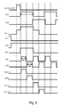
- Fig. 9 is time charts of the control signals HC1, HC2, LC1 and LC2, and the clock signals CK1 and CK2 for the shift register shown in Fig. 8 , the voltage potential of the node Q(n), the voltage potential of the output g(n), and the corresponding scanning signals G(2n-2), G(2n-1), G(2n), G(2n+1) and G(2n+2) generated by the shift register in response to the control signals and the clock signals.
- the high voltage pulse widths W H , W 1 and W 2 of the first control signal HC1, the first and second clock signals CK1 and CK2 obeys the relationship of W H ⁇ (W 1 + W 2 ).
- Fig. 10 is a simulated time charts of the control signals HC1, HC2, LC1 and LC2, and the clock signals CK1 and CK2 for the shift register shown in Fig. 8 , the voltage potential of the node Q(n), the voltage potential of the output g(n), and the corresponding scanning signals G(2n-2), G(2n-1), G(2n), G(2n+1) and G(2n+2) generated by the shift register in response to the control signals and the clock signals.
- a display panel 1100 with a GOA architecture 1101 of a shift register 1110 formed thereon is schematically shown according to another embodiment of the present invention.
- the display panel 1100 includes a substrate 1102 and a plurality of pixels 1104 spatially formed on the substrate 1102 defining a number of pixel rows. Each pixel row has a height of H.
- Each shift register stage S n is configured to receive one or more control and clock signals, for example, a control signal HCn and the j clock signals, CK1, CK2, ... and CKj, and to output responsively j scanning signals G(j*n-j+1), G(j*n-j+2), ... and G(j*n) for driving the (j*n-j+1)-th pixel row, (j*n-j+2)-th pixel row, ... and the (j*n)-th pixel row of the display panel 1100, respectively.
- Each stage S n includes a stage shift circuit and de-multiplexing circuit (not shown).
- the stage shift circuit is same as that disclosed above.
- the de-multiplexing circuit has j switch circuits, j being an integer greater than one.
- the de-multiplexing circuit is adapted for receiving the output signal from the stage shift circuit and j clock signals, CK1, CK2, ... and CKj from a data bus 1150 and responsively outputting j scanning signals, G(j*n-j+1), G(j*n-j+2), ... and G(j*n).
- Each switch circuit has the same circuit as shown in Figs. 3-8 and disclosed above. Specifically, each switch circuit has a first input for receiving a corresponding one of the j clock signals, CK1, CK2, ... and CKj, a second input electrically coupled to the output of the stage shift circuit for receiving the output signal therefrom, and an output for responsively outputting a corresponding one of the j scanning signals, G(j*n-j+1), G(j*n-j+2), ... and G(j*n).
- the first control signal HC n is a low frequency AC signal, while all the j clock signals, CK1, CK2, ... and CKj are high frequency AC signals.
- each of the first control signal HCn, and the j clock signals, CK1, CK2, ... and CKj is characterized with a waveform alternating between a high voltage level and a low voltage level, wherein the high voltage levels of the first control signal HC n , and the j clock signals, CK1, CK2, ... and CKj have widths, W H , W 1 , W 2 , ... and W j , respectively, satisfying the following relationship of: W H ⁇ W 1 + W 2 + ... + W j .
- the plurality of shift register stages ⁇ S n ⁇ is disposed spatially and sequentially on the substrate 1102 in such a way that the layout of each shift register stage S n has a height of (j*H), and the j scanning signals G(j*n-j+1), G(j*n-j+2), ... and G(j*n) output from the shift register stage S n are used to drive the (j*n-j+1)-th pixel row, (j*n-j+2)-th pixel row, ... and the (j*n)-th pixel row, respectively.
- the GOA architecture 1101 also includes a formation of a data bus 1150 on the substrate 1102 for providing, for example, the first control signal HC n , and the j clock signals CK1, CK2, ... and CKj for each the shift register stage S n .
- the circuit layout of the shift register on the substrate is substantially simplified.
Landscapes
- Engineering & Computer Science (AREA)
- Physics & Mathematics (AREA)
- Computer Hardware Design (AREA)
- General Physics & Mathematics (AREA)
- Theoretical Computer Science (AREA)
- Chemical & Material Sciences (AREA)
- Crystallography & Structural Chemistry (AREA)
- Control Of Indicators Other Than Cathode Ray Tubes (AREA)
- Liquid Crystal Display Device Control (AREA)
- Shift Register Type Memory (AREA)
Applications Claiming Priority (1)
| Application Number | Priority Date | Filing Date | Title |
|---|---|---|---|
| US12/823,237 US8325127B2 (en) | 2010-06-25 | 2010-06-25 | Shift register and architecture of same on a display panel |
Publications (1)
| Publication Number | Publication Date |
|---|---|
| EP2400481A1 true EP2400481A1 (de) | 2011-12-28 |
Family
ID=43548824
Family Applications (1)
| Application Number | Title | Priority Date | Filing Date |
|---|---|---|---|
| EP10193556A Withdrawn EP2400481A1 (de) | 2010-06-25 | 2010-12-02 | Schieberegister und seine Architektur auf einer Anzeigetafel |
Country Status (4)
| Country | Link |
|---|---|
| US (1) | US8325127B2 (de) |
| EP (1) | EP2400481A1 (de) |
| CN (1) | CN102226940B (de) |
| TW (1) | TWI412231B (de) |
Cited By (2)
| Publication number | Priority date | Publication date | Assignee | Title |
|---|---|---|---|---|
| EP2879126A4 (de) * | 2012-07-24 | 2016-01-20 | Beijing Boe Optoelectronics | Gate-treiberschaltung, verfahren und flüssigkristallanzeige |
| US10629149B2 (en) | 2013-07-10 | 2020-04-21 | Semiconductor Energy Laboratory Co., Ltd. | Semiconductor device, driver circuit, and display device |
Families Citing this family (48)
| Publication number | Priority date | Publication date | Assignee | Title |
|---|---|---|---|---|
| KR101804315B1 (ko) * | 2010-12-06 | 2018-01-11 | 삼성디스플레이 주식회사 | 표시 장치, 표시 장치를 위한 주사 구동 장치 및 그 구동 방법 |
| KR102070660B1 (ko) * | 2012-04-20 | 2020-01-30 | 삼성디스플레이 주식회사 | 표시 패널 및 이를 포함하는 표시 장치 |
| TWI459368B (zh) * | 2012-09-14 | 2014-11-01 | Au Optronics Corp | 顯示裝置及其閘極信號產生方法 |
| CN103268032B (zh) * | 2012-12-28 | 2016-07-06 | 上海中航光电子有限公司 | 一种阵列基板、显示面板和显示装置 |
| JP6110177B2 (ja) * | 2013-03-27 | 2017-04-05 | 京セラ株式会社 | シフトレジスタ回路および画像表示装置 |
| US9041453B2 (en) * | 2013-04-04 | 2015-05-26 | Semiconductor Energy Laboratory Co., Ltd. | Pulse generation circuit and semiconductor device |
| TWI498877B (zh) * | 2013-04-26 | 2015-09-01 | Chunghwa Picture Tubes Ltd | 顯示面板 |
| TWI584249B (zh) * | 2013-05-09 | 2017-05-21 | 友達光電股份有限公司 | 顯示面板與掃描電路 |
| CN103295515B (zh) * | 2013-05-24 | 2016-07-06 | 福建华映显示科技有限公司 | 显示面板 |
| CN103345911B (zh) * | 2013-06-26 | 2016-02-17 | 京东方科技集团股份有限公司 | 一种移位寄存器单元、栅极驱动电路及显示装置 |
| CN103474040B (zh) * | 2013-09-06 | 2015-06-24 | 合肥京东方光电科技有限公司 | 栅极驱动单元、栅极驱动电路和显示装置 |
| CN103680451B (zh) * | 2013-12-18 | 2015-12-30 | 深圳市华星光电技术有限公司 | 用于液晶显示的goa电路及显示装置 |
| CN103680386B (zh) * | 2013-12-18 | 2016-03-09 | 深圳市华星光电技术有限公司 | 用于平板显示的goa电路及显示装置 |
| CN103680388B (zh) * | 2013-12-26 | 2015-11-11 | 深圳市华星光电技术有限公司 | 用于平板显示的可修复的goa电路及显示装置 |
| CN103745700B (zh) * | 2013-12-27 | 2015-10-07 | 深圳市华星光电技术有限公司 | 自修复型栅极驱动电路 |
| TWI595472B (zh) * | 2014-06-23 | 2017-08-11 | 友達光電股份有限公司 | 顯示面板 |
| TWI546786B (zh) * | 2014-08-22 | 2016-08-21 | 友達光電股份有限公司 | 顯示面板 |
| US9437151B2 (en) * | 2014-09-04 | 2016-09-06 | Shenzhen China Star Optoelectronics Technology Co., Ltd | Scan driving circuit and display panel |
| CN104409054B (zh) * | 2014-11-03 | 2017-02-15 | 深圳市华星光电技术有限公司 | 低温多晶硅薄膜晶体管goa电路 |
| CN104464663B (zh) * | 2014-11-03 | 2017-02-15 | 深圳市华星光电技术有限公司 | 低温多晶硅薄膜晶体管goa电路 |
| TWI549107B (zh) * | 2014-11-05 | 2016-09-11 | 群創光電股份有限公司 | 顯示裝置 |
| CN104332144B (zh) * | 2014-11-05 | 2017-04-12 | 深圳市华星光电技术有限公司 | 液晶显示面板及其栅极驱动电路 |
| TWI552129B (zh) * | 2014-11-26 | 2016-10-01 | 群創光電股份有限公司 | 掃描驅動電路及應用其之顯示面板 |
| CN105702189B (zh) * | 2014-11-26 | 2019-10-08 | 群创光电股份有限公司 | 扫描驱动电路及应用其的显示面板 |
| CN104867439B (zh) * | 2015-06-24 | 2017-04-05 | 合肥京东方光电科技有限公司 | 移位寄存器单元及其驱动方法、栅极驱动电路及显示装置 |
| CN105096865B (zh) * | 2015-08-06 | 2018-09-07 | 京东方科技集团股份有限公司 | 移位寄存器的输出控制单元、移位寄存器及其驱动方法以及栅极驱动装置 |
| US20170084234A1 (en) * | 2015-09-23 | 2017-03-23 | Qualcomm Mems Technologies, Inc. | Driver circuits with shared node |
| TWI571848B (zh) * | 2015-11-06 | 2017-02-21 | 友達光電股份有限公司 | 閘極驅動電路 |
| CN106205528B (zh) * | 2016-07-19 | 2019-04-16 | 深圳市华星光电技术有限公司 | 一种goa电路及液晶显示面板 |
| CN106128392A (zh) * | 2016-08-29 | 2016-11-16 | 武汉华星光电技术有限公司 | Goa驱动电路和嵌入式触控显示面板 |
| CN108694894B (zh) * | 2017-04-05 | 2020-07-07 | 京东方科技集团股份有限公司 | 移位缓存及栅极驱动电路、显示面板及设备和驱动方法 |
| CN107093415B (zh) * | 2017-07-04 | 2019-09-03 | 京东方科技集团股份有限公司 | 栅极驱动电路、驱动方法和显示装置 |
| CN107862998B (zh) * | 2017-11-09 | 2020-05-19 | 深圳市华星光电半导体显示技术有限公司 | 一种柔性goa显示面板及其制作方法 |
| CN107705757B (zh) * | 2017-11-27 | 2019-10-18 | 京东方科技集团股份有限公司 | 移位寄存器及其分时控制方法、显示面板和装置 |
| CN108122529B (zh) * | 2018-01-25 | 2021-08-17 | 京东方科技集团股份有限公司 | 栅极驱动单元及其驱动方法和栅极驱动电路 |
| CN110111830A (zh) * | 2018-02-01 | 2019-08-09 | 中华映管股份有限公司 | 位移暂存装置 |
| CN109785789B (zh) * | 2018-04-18 | 2021-11-16 | 友达光电股份有限公司 | 多工器以及显示面板 |
| TWI683114B (zh) * | 2018-11-28 | 2020-01-21 | 友達光電股份有限公司 | 顯示面板 |
| CN109448657A (zh) * | 2018-12-26 | 2019-03-08 | 惠科股份有限公司 | 移位暂存器和栅极驱动电路 |
| CN109801582B (zh) * | 2019-02-27 | 2022-06-03 | 南京京东方显示技术有限公司 | 一种自驱动像素电路及显示装置 |
| US11538428B2 (en) * | 2019-03-01 | 2022-12-27 | Chongqing Boe Optoelectronics Technology Co., Ltd. | Shift register and drive method thereof, and gate drive circuit |
| CN113496681A (zh) * | 2020-03-18 | 2021-10-12 | Tcl华星光电技术有限公司 | 一种goa电路及显示面板 |
| CN113906492B (zh) * | 2020-03-27 | 2023-04-28 | 京东方科技集团股份有限公司 | 栅极驱动电路及其驱动方法、显示面板 |
| TWI756969B (zh) | 2020-12-07 | 2022-03-01 | 友達光電股份有限公司 | 移位暫存器電路 |
| TWI763235B (zh) | 2021-01-06 | 2022-05-01 | 友達光電股份有限公司 | 顯示面板 |
| TWI781512B (zh) * | 2021-01-12 | 2022-10-21 | 友達光電股份有限公司 | 畫素驅動裝置 |
| TWI774330B (zh) * | 2021-04-21 | 2022-08-11 | 友達光電股份有限公司 | 閘極驅動裝置及顯示面板 |
| TWI769910B (zh) * | 2021-08-11 | 2022-07-01 | 友達光電股份有限公司 | 閘極驅動電路及包含其之顯示面板 |
Citations (8)
| Publication number | Priority date | Publication date | Assignee | Title |
|---|---|---|---|---|
| US20020080108A1 (en) * | 2000-12-26 | 2002-06-27 | Hannstar Display Corp. | Gate lines driving circuit and driving method |
| US20020163493A1 (en) * | 1998-03-30 | 2002-11-07 | Sharp Kabushiki Kaisha | Liquid crystal display device and method of driving same |
| US20060267909A1 (en) * | 2005-05-25 | 2006-11-30 | Chih-Hsin Hsu | Gate switch apparatus for amorphous silicon lcd |
| US20080122774A1 (en) * | 2006-06-26 | 2008-05-29 | Sung Hak Jo | Apparatus and method of driving liquid crystal display device |
| US20080165112A1 (en) * | 2007-01-09 | 2008-07-10 | Denmos Technology Inc. | Gate driver |
| EP1983500A2 (de) * | 2007-04-16 | 2008-10-22 | TPO Displays Corp. | Abtastsignalgenerator für Matrixanzeige |
| US20080266275A1 (en) * | 2007-04-25 | 2008-10-30 | Wintek Corporation | Shift register and liquid crystal display |
| EP2313881A1 (de) * | 2008-07-29 | 2011-04-27 | Ignis Innovation Inc. Et Al | Verfahren und system zur ansteuerung einer lichtemittierenden anzeige |
Family Cites Families (2)
| Publication number | Priority date | Publication date | Assignee | Title |
|---|---|---|---|---|
| JP2000031084A (ja) | 1998-05-08 | 2000-01-28 | Samsung Electron Co Ltd | 化合物半導体薄膜のp型への活性化方法 |
| TWI320564B (en) * | 2005-08-25 | 2010-02-11 | Au Optronics Corp | A shift register driving method |
-
2010
- 2010-06-25 US US12/823,237 patent/US8325127B2/en active Active
- 2010-12-02 EP EP10193556A patent/EP2400481A1/de not_active Withdrawn
- 2010-12-22 TW TW099145286A patent/TWI412231B/zh active
-
2011
- 2011-06-10 CN CN2011101651561A patent/CN102226940B/zh active Active
Patent Citations (8)
| Publication number | Priority date | Publication date | Assignee | Title |
|---|---|---|---|---|
| US20020163493A1 (en) * | 1998-03-30 | 2002-11-07 | Sharp Kabushiki Kaisha | Liquid crystal display device and method of driving same |
| US20020080108A1 (en) * | 2000-12-26 | 2002-06-27 | Hannstar Display Corp. | Gate lines driving circuit and driving method |
| US20060267909A1 (en) * | 2005-05-25 | 2006-11-30 | Chih-Hsin Hsu | Gate switch apparatus for amorphous silicon lcd |
| US20080122774A1 (en) * | 2006-06-26 | 2008-05-29 | Sung Hak Jo | Apparatus and method of driving liquid crystal display device |
| US20080165112A1 (en) * | 2007-01-09 | 2008-07-10 | Denmos Technology Inc. | Gate driver |
| EP1983500A2 (de) * | 2007-04-16 | 2008-10-22 | TPO Displays Corp. | Abtastsignalgenerator für Matrixanzeige |
| US20080266275A1 (en) * | 2007-04-25 | 2008-10-30 | Wintek Corporation | Shift register and liquid crystal display |
| EP2313881A1 (de) * | 2008-07-29 | 2011-04-27 | Ignis Innovation Inc. Et Al | Verfahren und system zur ansteuerung einer lichtemittierenden anzeige |
Cited By (5)
| Publication number | Priority date | Publication date | Assignee | Title |
|---|---|---|---|---|
| EP2879126A4 (de) * | 2012-07-24 | 2016-01-20 | Beijing Boe Optoelectronics | Gate-treiberschaltung, verfahren und flüssigkristallanzeige |
| US9886921B2 (en) | 2012-07-24 | 2018-02-06 | Beijing Boe Optoelectronics Technology Co., Ltd. | Gate driving circuit, gate driving method, and liquid crystal display |
| US10629149B2 (en) | 2013-07-10 | 2020-04-21 | Semiconductor Energy Laboratory Co., Ltd. | Semiconductor device, driver circuit, and display device |
| US11308910B2 (en) | 2013-07-10 | 2022-04-19 | Semiconductor Energy Laboratory Co., Ltd. | Display device comprising a transistor with LDD regions |
| US11869453B2 (en) | 2013-07-10 | 2024-01-09 | Semiconductor Energy Laboratory Co., Ltd. | Display device comprising semiconductor layer having LDD regions |
Also Published As
| Publication number | Publication date |
|---|---|
| CN102226940B (zh) | 2013-05-22 |
| TWI412231B (zh) | 2013-10-11 |
| CN102226940A (zh) | 2011-10-26 |
| US8325127B2 (en) | 2012-12-04 |
| TW201201514A (en) | 2012-01-01 |
| US20110316833A1 (en) | 2011-12-29 |
Similar Documents
| Publication | Publication Date | Title |
|---|---|---|
| EP2400481A1 (de) | Schieberegister und seine Architektur auf einer Anzeigetafel | |
| JP5165153B2 (ja) | 走査信号線駆動回路およびそれを備えた表示装置、ならびに走査信号線の駆動方法 | |
| JP5132818B2 (ja) | 走査信号線駆動回路およびそれを備えた表示装置 | |
| US7817771B2 (en) | Shift register | |
| JP5230853B2 (ja) | 走査信号線駆動回路およびそれを備えた表示装置 | |
| EP2234098B1 (de) | Anzeigevorrichtung und verfahren zum betrieb der anzeigevorrichtung | |
| EP2369594B1 (de) | Schieberegister mit geringem Leistungsverbrauch | |
| EP2302617B1 (de) | Klappsteuerschaltung und Schieberegister zur Verwendung damit | |
| US8102962B2 (en) | Bidrectional shifter register and method of driving same | |
| JP5349693B2 (ja) | 走査信号線駆動回路および走査信号線の駆動方法 | |
| TWI529682B (zh) | A scanning signal line driving circuit, a display device including the same, and a driving method of a scanning signal line | |
| WO2014092011A1 (ja) | 表示装置およびその駆動方法 | |
| WO2011055584A1 (ja) | 液晶表示装置およびその駆動方法 | |
| WO2011104945A1 (ja) | 表示装置 | |
| WO2011148658A1 (ja) | 走査信号線駆動回路およびそれを備えた表示装置 | |
| US20130069930A1 (en) | Shift register, scanning signal line drive circuit, and display device | |
| WO2011129126A1 (ja) | 走査信号線駆動回路およびそれを備えた表示装置 | |
| US9336736B2 (en) | Liquid crystal display device and method for driving auxiliary capacitance lines | |
| WO2011036911A1 (ja) | 液晶表示装置 | |
| US20130201090A1 (en) | Liquid crystal display device | |
| TWI776554B (zh) | 移位暫存器及顯示裝置 | |
| JP6076253B2 (ja) | 表示装置およびその駆動方法 |
Legal Events
| Date | Code | Title | Description |
|---|---|---|---|
| 17P | Request for examination filed |
Effective date: 20101230 |
|
| AK | Designated contracting states |
Kind code of ref document: A1 Designated state(s): AL AT BE BG CH CY CZ DE DK EE ES FI FR GB GR HR HU IE IS IT LI LT LU LV MC MK MT NL NO PL PT RO RS SE SI SK SM TR |
|
| AX | Request for extension of the european patent |
Extension state: BA ME |
|
| PUAI | Public reference made under article 153(3) epc to a published international application that has entered the european phase |
Free format text: ORIGINAL CODE: 0009012 |
|
| 17Q | First examination report despatched |
Effective date: 20120723 |
|
| STAA | Information on the status of an ep patent application or granted ep patent |
Free format text: STATUS: THE APPLICATION IS DEEMED TO BE WITHDRAWN |
|
| 18D | Application deemed to be withdrawn |
Effective date: 20160803 |