EP2380045B1 - Articles antireflet et leurs procédés de fabrication - Google Patents
Articles antireflet et leurs procédés de fabrication Download PDFInfo
- Publication number
- EP2380045B1 EP2380045B1 EP09808972.5A EP09808972A EP2380045B1 EP 2380045 B1 EP2380045 B1 EP 2380045B1 EP 09808972 A EP09808972 A EP 09808972A EP 2380045 B1 EP2380045 B1 EP 2380045B1
- Authority
- EP
- European Patent Office
- Prior art keywords
- substrate
- composite
- matrix
- electrode
- acrylate
- Prior art date
- Legal status (The legal status is an assumption and is not a legal conclusion. Google has not performed a legal analysis and makes no representation as to the accuracy of the status listed.)
- Not-in-force
Links
Images


Classifications
-
- G—PHYSICS
- G02—OPTICS
- G02B—OPTICAL ELEMENTS, SYSTEMS OR APPARATUS
- G02B1/00—Optical elements characterised by the material of which they are made; Optical coatings for optical elements
- G02B1/10—Optical coatings produced by application to, or surface treatment of, optical elements
- G02B1/11—Anti-reflection coatings
- G02B1/118—Anti-reflection coatings having sub-optical wavelength surface structures designed to provide an enhanced transmittance, e.g. moth-eye structures
-
- B—PERFORMING OPERATIONS; TRANSPORTING
- B05—SPRAYING OR ATOMISING IN GENERAL; APPLYING FLUENT MATERIALS TO SURFACES, IN GENERAL
- B05D—PROCESSES FOR APPLYING FLUENT MATERIALS TO SURFACES, IN GENERAL
- B05D3/00—Pretreatment of surfaces to which liquids or other fluent materials are to be applied; After-treatment of applied coatings, e.g. intermediate treating of an applied coating preparatory to subsequent applications of liquids or other fluent materials
- B05D3/10—Pretreatment of surfaces to which liquids or other fluent materials are to be applied; After-treatment of applied coatings, e.g. intermediate treating of an applied coating preparatory to subsequent applications of liquids or other fluent materials by other chemical means
- B05D3/107—Post-treatment of applied coatings
-
- B—PERFORMING OPERATIONS; TRANSPORTING
- B05—SPRAYING OR ATOMISING IN GENERAL; APPLYING FLUENT MATERIALS TO SURFACES, IN GENERAL
- B05D—PROCESSES FOR APPLYING FLUENT MATERIALS TO SURFACES, IN GENERAL
- B05D5/00—Processes for applying liquids or other fluent materials to surfaces to obtain special surface effects, finishes or structures
- B05D5/06—Processes for applying liquids or other fluent materials to surfaces to obtain special surface effects, finishes or structures to obtain multicolour or other optical effects
-
- B—PERFORMING OPERATIONS; TRANSPORTING
- B32—LAYERED PRODUCTS
- B32B—LAYERED PRODUCTS, i.e. PRODUCTS BUILT-UP OF STRATA OF FLAT OR NON-FLAT, e.g. CELLULAR OR HONEYCOMB, FORM
- B32B17/00—Layered products essentially comprising sheet glass, or glass, slag, or like fibres
- B32B17/06—Layered products essentially comprising sheet glass, or glass, slag, or like fibres comprising glass as the main or only constituent of a layer, next to another layer of a specific material
-
- B—PERFORMING OPERATIONS; TRANSPORTING
- B32—LAYERED PRODUCTS
- B32B—LAYERED PRODUCTS, i.e. PRODUCTS BUILT-UP OF STRATA OF FLAT OR NON-FLAT, e.g. CELLULAR OR HONEYCOMB, FORM
- B32B37/00—Methods or apparatus for laminating, e.g. by curing or by ultrasonic bonding
- B32B37/02—Methods or apparatus for laminating, e.g. by curing or by ultrasonic bonding characterised by a sequence of laminating steps, e.g. by adding new layers at consecutive laminating stations
-
- B—PERFORMING OPERATIONS; TRANSPORTING
- B32—LAYERED PRODUCTS
- B32B—LAYERED PRODUCTS, i.e. PRODUCTS BUILT-UP OF STRATA OF FLAT OR NON-FLAT, e.g. CELLULAR OR HONEYCOMB, FORM
- B32B38/00—Ancillary operations in connection with laminating processes
- B32B38/0008—Electrical discharge treatment, e.g. corona, plasma treatment; wave energy or particle radiation
-
- B—PERFORMING OPERATIONS; TRANSPORTING
- B32—LAYERED PRODUCTS
- B32B—LAYERED PRODUCTS, i.e. PRODUCTS BUILT-UP OF STRATA OF FLAT OR NON-FLAT, e.g. CELLULAR OR HONEYCOMB, FORM
- B32B7/00—Layered products characterised by the relation between layers; Layered products characterised by the relative orientation of features between layers, or by the relative values of a measurable parameter between layers, i.e. products comprising layers having different physical, chemical or physicochemical properties; Layered products characterised by the interconnection of layers
- B32B7/04—Interconnection of layers
- B32B7/12—Interconnection of layers using interposed adhesives or interposed materials with bonding properties
-
- C—CHEMISTRY; METALLURGY
- C08—ORGANIC MACROMOLECULAR COMPOUNDS; THEIR PREPARATION OR CHEMICAL WORKING-UP; COMPOSITIONS BASED THEREON
- C08J—WORKING-UP; GENERAL PROCESSES OF COMPOUNDING; AFTER-TREATMENT NOT COVERED BY SUBCLASSES C08B, C08C, C08F, C08G or C08H
- C08J7/00—Chemical treatment or coating of shaped articles made of macromolecular substances
- C08J7/04—Coating
- C08J7/042—Coating with two or more layers, where at least one layer of a composition contains a polymer binder
- C08J7/0423—Coating with two or more layers, where at least one layer of a composition contains a polymer binder with at least one layer of inorganic material and at least one layer of a composition containing a polymer binder
-
- C—CHEMISTRY; METALLURGY
- C08—ORGANIC MACROMOLECULAR COMPOUNDS; THEIR PREPARATION OR CHEMICAL WORKING-UP; COMPOSITIONS BASED THEREON
- C08J—WORKING-UP; GENERAL PROCESSES OF COMPOUNDING; AFTER-TREATMENT NOT COVERED BY SUBCLASSES C08B, C08C, C08F, C08G or C08H
- C08J7/00—Chemical treatment or coating of shaped articles made of macromolecular substances
- C08J7/04—Coating
- C08J7/043—Improving the adhesiveness of the coatings per se, e.g. forming primers
-
- C—CHEMISTRY; METALLURGY
- C08—ORGANIC MACROMOLECULAR COMPOUNDS; THEIR PREPARATION OR CHEMICAL WORKING-UP; COMPOSITIONS BASED THEREON
- C08J—WORKING-UP; GENERAL PROCESSES OF COMPOUNDING; AFTER-TREATMENT NOT COVERED BY SUBCLASSES C08B, C08C, C08F, C08G or C08H
- C08J7/00—Chemical treatment or coating of shaped articles made of macromolecular substances
- C08J7/04—Coating
- C08J7/044—Forming conductive coatings; Forming coatings having anti-static properties
-
- C—CHEMISTRY; METALLURGY
- C08—ORGANIC MACROMOLECULAR COMPOUNDS; THEIR PREPARATION OR CHEMICAL WORKING-UP; COMPOSITIONS BASED THEREON
- C08J—WORKING-UP; GENERAL PROCESSES OF COMPOUNDING; AFTER-TREATMENT NOT COVERED BY SUBCLASSES C08B, C08C, C08F, C08G or C08H
- C08J7/00—Chemical treatment or coating of shaped articles made of macromolecular substances
- C08J7/04—Coating
- C08J7/046—Forming abrasion-resistant coatings; Forming surface-hardening coatings
-
- C—CHEMISTRY; METALLURGY
- C08—ORGANIC MACROMOLECULAR COMPOUNDS; THEIR PREPARATION OR CHEMICAL WORKING-UP; COMPOSITIONS BASED THEREON
- C08J—WORKING-UP; GENERAL PROCESSES OF COMPOUNDING; AFTER-TREATMENT NOT COVERED BY SUBCLASSES C08B, C08C, C08F, C08G or C08H
- C08J7/00—Chemical treatment or coating of shaped articles made of macromolecular substances
- C08J7/04—Coating
- C08J7/054—Forming anti-misting or drip-proofing coatings
-
- C—CHEMISTRY; METALLURGY
- C08—ORGANIC MACROMOLECULAR COMPOUNDS; THEIR PREPARATION OR CHEMICAL WORKING-UP; COMPOSITIONS BASED THEREON
- C08J—WORKING-UP; GENERAL PROCESSES OF COMPOUNDING; AFTER-TREATMENT NOT COVERED BY SUBCLASSES C08B, C08C, C08F, C08G or C08H
- C08J7/00—Chemical treatment or coating of shaped articles made of macromolecular substances
- C08J7/04—Coating
- C08J7/056—Forming hydrophilic coatings
-
- C—CHEMISTRY; METALLURGY
- C08—ORGANIC MACROMOLECULAR COMPOUNDS; THEIR PREPARATION OR CHEMICAL WORKING-UP; COMPOSITIONS BASED THEREON
- C08J—WORKING-UP; GENERAL PROCESSES OF COMPOUNDING; AFTER-TREATMENT NOT COVERED BY SUBCLASSES C08B, C08C, C08F, C08G or C08H
- C08J7/00—Chemical treatment or coating of shaped articles made of macromolecular substances
- C08J7/12—Chemical modification
- C08J7/123—Treatment by wave energy or particle radiation
-
- G—PHYSICS
- G02—OPTICS
- G02B—OPTICAL ELEMENTS, SYSTEMS OR APPARATUS
- G02B1/00—Optical elements characterised by the material of which they are made; Optical coatings for optical elements
- G02B1/10—Optical coatings produced by application to, or surface treatment of, optical elements
- G02B1/11—Anti-reflection coatings
- G02B1/111—Anti-reflection coatings using layers comprising organic materials
-
- G—PHYSICS
- G02—OPTICS
- G02B—OPTICAL ELEMENTS, SYSTEMS OR APPARATUS
- G02B1/00—Optical elements characterised by the material of which they are made; Optical coatings for optical elements
- G02B1/10—Optical coatings produced by application to, or surface treatment of, optical elements
- G02B1/12—Optical coatings produced by application to, or surface treatment of, optical elements by surface treatment, e.g. by irradiation
-
- G—PHYSICS
- G02—OPTICS
- G02B—OPTICAL ELEMENTS, SYSTEMS OR APPARATUS
- G02B1/00—Optical elements characterised by the material of which they are made; Optical coatings for optical elements
- G02B1/10—Optical coatings produced by application to, or surface treatment of, optical elements
- G02B1/14—Protective coatings, e.g. hard coatings
-
- G—PHYSICS
- G02—OPTICS
- G02B—OPTICAL ELEMENTS, SYSTEMS OR APPARATUS
- G02B1/00—Optical elements characterised by the material of which they are made; Optical coatings for optical elements
- G02B1/10—Optical coatings produced by application to, or surface treatment of, optical elements
- G02B1/18—Coatings for keeping optical surfaces clean, e.g. hydrophobic or photo-catalytic films
-
- G—PHYSICS
- G02—OPTICS
- G02B—OPTICAL ELEMENTS, SYSTEMS OR APPARATUS
- G02B27/00—Optical systems or apparatus not provided for by any of the groups G02B1/00 - G02B26/00, G02B30/00
- G02B27/0006—Optical systems or apparatus not provided for by any of the groups G02B1/00 - G02B26/00, G02B30/00 with means to keep optical surfaces clean, e.g. by preventing or removing dirt, stains, contamination, condensation
-
- B—PERFORMING OPERATIONS; TRANSPORTING
- B32—LAYERED PRODUCTS
- B32B—LAYERED PRODUCTS, i.e. PRODUCTS BUILT-UP OF STRATA OF FLAT OR NON-FLAT, e.g. CELLULAR OR HONEYCOMB, FORM
- B32B2255/00—Coating on the layer surface
- B32B2255/26—Polymeric coating
-
- B—PERFORMING OPERATIONS; TRANSPORTING
- B32—LAYERED PRODUCTS
- B32B—LAYERED PRODUCTS, i.e. PRODUCTS BUILT-UP OF STRATA OF FLAT OR NON-FLAT, e.g. CELLULAR OR HONEYCOMB, FORM
- B32B2307/00—Properties of the layers or laminate
- B32B2307/40—Properties of the layers or laminate having particular optical properties
- B32B2307/412—Transparent
-
- B—PERFORMING OPERATIONS; TRANSPORTING
- B32—LAYERED PRODUCTS
- B32B—LAYERED PRODUCTS, i.e. PRODUCTS BUILT-UP OF STRATA OF FLAT OR NON-FLAT, e.g. CELLULAR OR HONEYCOMB, FORM
- B32B2307/00—Properties of the layers or laminate
- B32B2307/40—Properties of the layers or laminate having particular optical properties
- B32B2307/42—Polarizing, birefringent, filtering
-
- B—PERFORMING OPERATIONS; TRANSPORTING
- B32—LAYERED PRODUCTS
- B32B—LAYERED PRODUCTS, i.e. PRODUCTS BUILT-UP OF STRATA OF FLAT OR NON-FLAT, e.g. CELLULAR OR HONEYCOMB, FORM
- B32B2457/00—Electrical equipment
- B32B2457/20—Displays, e.g. liquid crystal displays, plasma displays
-
- B—PERFORMING OPERATIONS; TRANSPORTING
- B32—LAYERED PRODUCTS
- B32B—LAYERED PRODUCTS, i.e. PRODUCTS BUILT-UP OF STRATA OF FLAT OR NON-FLAT, e.g. CELLULAR OR HONEYCOMB, FORM
- B32B2457/00—Electrical equipment
- B32B2457/20—Displays, e.g. liquid crystal displays, plasma displays
- B32B2457/202—LCD, i.e. liquid crystal displays
-
- B—PERFORMING OPERATIONS; TRANSPORTING
- B32—LAYERED PRODUCTS
- B32B—LAYERED PRODUCTS, i.e. PRODUCTS BUILT-UP OF STRATA OF FLAT OR NON-FLAT, e.g. CELLULAR OR HONEYCOMB, FORM
- B32B2551/00—Optical elements
-
- C—CHEMISTRY; METALLURGY
- C08—ORGANIC MACROMOLECULAR COMPOUNDS; THEIR PREPARATION OR CHEMICAL WORKING-UP; COMPOSITIONS BASED THEREON
- C08J—WORKING-UP; GENERAL PROCESSES OF COMPOUNDING; AFTER-TREATMENT NOT COVERED BY SUBCLASSES C08B, C08C, C08F, C08G or C08H
- C08J2323/00—Characterised by the use of homopolymers or copolymers of unsaturated aliphatic hydrocarbons having only one carbon-to-carbon double bond; Derivatives of such polymers
- C08J2323/02—Characterised by the use of homopolymers or copolymers of unsaturated aliphatic hydrocarbons having only one carbon-to-carbon double bond; Derivatives of such polymers not modified by chemical after treatment
- C08J2323/04—Homopolymers or copolymers of ethene
- C08J2323/06—Polyethene
-
- C—CHEMISTRY; METALLURGY
- C08—ORGANIC MACROMOLECULAR COMPOUNDS; THEIR PREPARATION OR CHEMICAL WORKING-UP; COMPOSITIONS BASED THEREON
- C08J—WORKING-UP; GENERAL PROCESSES OF COMPOUNDING; AFTER-TREATMENT NOT COVERED BY SUBCLASSES C08B, C08C, C08F, C08G or C08H
- C08J2367/00—Characterised by the use of polyesters obtained by reactions forming a carboxylic ester link in the main chain; Derivatives of such polymers
- C08J2367/02—Polyesters derived from dicarboxylic acids and dihydroxy compounds
-
- C—CHEMISTRY; METALLURGY
- C08—ORGANIC MACROMOLECULAR COMPOUNDS; THEIR PREPARATION OR CHEMICAL WORKING-UP; COMPOSITIONS BASED THEREON
- C08J—WORKING-UP; GENERAL PROCESSES OF COMPOUNDING; AFTER-TREATMENT NOT COVERED BY SUBCLASSES C08B, C08C, C08F, C08G or C08H
- C08J2433/00—Characterised by the use of homopolymers or copolymers of compounds having one or more unsaturated aliphatic radicals, each having only one carbon-to-carbon double bond, and only one being terminated by only one carboxyl radical, or of salts, anhydrides, esters, amides, imides, or nitriles thereof; Derivatives of such polymers
- C08J2433/04—Characterised by the use of homopolymers or copolymers of compounds having one or more unsaturated aliphatic radicals, each having only one carbon-to-carbon double bond, and only one being terminated by only one carboxyl radical, or of salts, anhydrides, esters, amides, imides, or nitriles thereof; Derivatives of such polymers esters
- C08J2433/06—Characterised by the use of homopolymers or copolymers of compounds having one or more unsaturated aliphatic radicals, each having only one carbon-to-carbon double bond, and only one being terminated by only one carboxyl radical, or of salts, anhydrides, esters, amides, imides, or nitriles thereof; Derivatives of such polymers esters of esters containing only carbon, hydrogen, and oxygen, the oxygen atom being present only as part of the carboxyl radical
- C08J2433/08—Homopolymers or copolymers of acrylic acid esters
-
- C—CHEMISTRY; METALLURGY
- C08—ORGANIC MACROMOLECULAR COMPOUNDS; THEIR PREPARATION OR CHEMICAL WORKING-UP; COMPOSITIONS BASED THEREON
- C08J—WORKING-UP; GENERAL PROCESSES OF COMPOUNDING; AFTER-TREATMENT NOT COVERED BY SUBCLASSES C08B, C08C, C08F, C08G or C08H
- C08J2483/00—Characterised by the use of macromolecular compounds obtained by reactions forming in the main chain of the macromolecule a linkage containing silicon with or without sulfur, nitrogen, oxygen, or carbon only; Derivatives of such polymers
- C08J2483/02—Polysilicates
-
- F—MECHANICAL ENGINEERING; LIGHTING; HEATING; WEAPONS; BLASTING
- F24—HEATING; RANGES; VENTILATING
- F24S—SOLAR HEAT COLLECTORS; SOLAR HEAT SYSTEMS
- F24S70/00—Details of absorbing elements
- F24S70/10—Details of absorbing elements characterised by the absorbing material
-
- F—MECHANICAL ENGINEERING; LIGHTING; HEATING; WEAPONS; BLASTING
- F24—HEATING; RANGES; VENTILATING
- F24S—SOLAR HEAT COLLECTORS; SOLAR HEAT SYSTEMS
- F24S70/00—Details of absorbing elements
- F24S70/60—Details of absorbing elements characterised by the structure or construction
-
- Y—GENERAL TAGGING OF NEW TECHNOLOGICAL DEVELOPMENTS; GENERAL TAGGING OF CROSS-SECTIONAL TECHNOLOGIES SPANNING OVER SEVERAL SECTIONS OF THE IPC; TECHNICAL SUBJECTS COVERED BY FORMER USPC CROSS-REFERENCE ART COLLECTIONS [XRACs] AND DIGESTS
- Y10—TECHNICAL SUBJECTS COVERED BY FORMER USPC
- Y10T—TECHNICAL SUBJECTS COVERED BY FORMER US CLASSIFICATION
- Y10T428/00—Stock material or miscellaneous articles
- Y10T428/25—Web or sheet containing structurally defined element or component and including a second component containing structurally defined particles
- Y10T428/254—Polymeric or resinous material
-
- Y—GENERAL TAGGING OF NEW TECHNOLOGICAL DEVELOPMENTS; GENERAL TAGGING OF CROSS-SECTIONAL TECHNOLOGIES SPANNING OVER SEVERAL SECTIONS OF THE IPC; TECHNICAL SUBJECTS COVERED BY FORMER USPC CROSS-REFERENCE ART COLLECTIONS [XRACs] AND DIGESTS
- Y10—TECHNICAL SUBJECTS COVERED BY FORMER USPC
- Y10T—TECHNICAL SUBJECTS COVERED BY FORMER US CLASSIFICATION
- Y10T428/00—Stock material or miscellaneous articles
- Y10T428/25—Web or sheet containing structurally defined element or component and including a second component containing structurally defined particles
- Y10T428/256—Heavy metal or aluminum or compound thereof
- Y10T428/257—Iron oxide or aluminum oxide
-
- Y—GENERAL TAGGING OF NEW TECHNOLOGICAL DEVELOPMENTS; GENERAL TAGGING OF CROSS-SECTIONAL TECHNOLOGIES SPANNING OVER SEVERAL SECTIONS OF THE IPC; TECHNICAL SUBJECTS COVERED BY FORMER USPC CROSS-REFERENCE ART COLLECTIONS [XRACs] AND DIGESTS
- Y10—TECHNICAL SUBJECTS COVERED BY FORMER USPC
- Y10T—TECHNICAL SUBJECTS COVERED BY FORMER US CLASSIFICATION
- Y10T428/00—Stock material or miscellaneous articles
- Y10T428/25—Web or sheet containing structurally defined element or component and including a second component containing structurally defined particles
- Y10T428/258—Alkali metal or alkaline earth metal or compound thereof
-
- Y—GENERAL TAGGING OF NEW TECHNOLOGICAL DEVELOPMENTS; GENERAL TAGGING OF CROSS-SECTIONAL TECHNOLOGIES SPANNING OVER SEVERAL SECTIONS OF THE IPC; TECHNICAL SUBJECTS COVERED BY FORMER USPC CROSS-REFERENCE ART COLLECTIONS [XRACs] AND DIGESTS
- Y10—TECHNICAL SUBJECTS COVERED BY FORMER USPC
- Y10T—TECHNICAL SUBJECTS COVERED BY FORMER US CLASSIFICATION
- Y10T428/00—Stock material or miscellaneous articles
- Y10T428/25—Web or sheet containing structurally defined element or component and including a second component containing structurally defined particles
- Y10T428/259—Silicic material
-
- Y—GENERAL TAGGING OF NEW TECHNOLOGICAL DEVELOPMENTS; GENERAL TAGGING OF CROSS-SECTIONAL TECHNOLOGIES SPANNING OVER SEVERAL SECTIONS OF THE IPC; TECHNICAL SUBJECTS COVERED BY FORMER USPC CROSS-REFERENCE ART COLLECTIONS [XRACs] AND DIGESTS
- Y10—TECHNICAL SUBJECTS COVERED BY FORMER USPC
- Y10T—TECHNICAL SUBJECTS COVERED BY FORMER US CLASSIFICATION
- Y10T428/00—Stock material or miscellaneous articles
- Y10T428/28—Web or sheet containing structurally defined element or component and having an adhesive outermost layer
- Y10T428/2848—Three or more layers
Definitions
- This invention relates to nanostructured articles that are useful, for example, as antireflective articles. In another aspect, this invention relates to methods for making nanostructured articles.
- AR antireflective
- subwavelength surface structure for example, subwavelength scale surface gratings
- broadband antireflection For example, the methods for creating the subwavelength surface structure tend to be complicated and expensive batch processes, however.
- the method disclosed in U.S. Patent Application Pub. No. 2005/0233083 involves bombarding a polymeric surface with Ar/O 2 plasma under vacuum conditions of less than 0.07 Pa (0.5mTorr). This requirement of extreme vacuum conditions limits the commercial viability of the method.
- US 2008/174875 A1 describes an optical layered body which improves preventing scintillation property, gloss blackness, color reproducibility (preventing coloring and interference fringe) while maintaining antistatic performance and an antiglare property, and provides an optical layered body comprising an antistatic layer, an antiglare layer and a low refractive index layer in an order on a light-transmitting substrate, wherein said antistatic layer is a resin thin layer containing antimony-doped tin oxide and a diffusion filler, and having surface roughness on its surface.
- the surface roughness on the surface of the antistatic layer may be formed with the diffusion filler, the antiglare layer may have a surface roughness on its surface formed with an antiglare agent, for example non-spherical silica and organic particles, on its surface, wherein the surface roughness on the antistatic layer and the surface roughness on the antiglare layer are preferably separately formed.
- the optical layer body may be included in an image display device, such as an LCD including a light-transmitting display and a light source apparatus to irradiate the light-transmitting display. A light source of the light source apparatus may irradiate from the side on which the light-transmitting substrate exists of the optical layered body.
- An adhesive layer may be provided between the respective layers of a liquid crystal display device as required.
- the present invention relates to a nanostructured article comprising a matrix and a nanoscale dispersed phase, and having a random nanostructured anisotropic surface.
- nanoscale means submicron (for example, between about 1nm and about 500nm); “nanostructured” means having one dimension on the nanoscale; and “anisotropic surface” means a surface having structural asperities having a height to width (that is, average width) ratio of about 1.5:1 or greater (preferably, 2:1 or greater; more preferably, 5:1 or greater).
- the nanostructured articles exhibit a significant reduction in reflectance compared to an unstructured article comprising the same matrix material and nanodispersed phase.
- the nanostructured articles can be durable and possess scratch resistance.
- Some embodiments of the nanostructured articles also exhibit additional desirable properties such as, for example, antifogging, easy cleaning, antimicrobial activity, hydrophilicity, or hydrophobicity.
- a method of making random nanostructured surfaces may comprise providing a matrix comprising a nanodispersed phase, and anisotropically etching the matrix using plasma to form a random nanostructured anisotropic surface. Another method may comprise providing a matrix comprising a nanodispersed phase, and etching at least a portion of the nanodispersed phase using plasma to form a random nanostructured surface.
- the present disclosure provides a composite as defined by independent claim 1 comprising:
- the present disclosure provides a method of making a composite as defined by independent claim 14, comprising the steps of: (a) providing a substrate having at least 90% transmission in visible light and less than 5% haze; (b) coating a hardcoat composition on the first major surface of the substrate to yield a antireflective layer, the hardcoat composition comprising nanoparticles of SiO 2 , ZrO 2 and combinations thereof, the nanoparticles dispersed in a matrix; (c) drying the hardcoat solution to yield an antireflective layer; (d) exposing the antireflective layer to reactive ion etching comprising the steps of (i) placing the antireflective layer on a cylindrical electrode in a vacuum vessel, (ii) introducing etchant gas to the vessel at a predetermined pressure, (iii) generating plasma between the cylindrical electrode and a counter-electrode; (iv) rotating the cylindrical electrode to translate the substrate; and (v) anisotropically etching the hardcoat composition; and (e)
- plasma means a partially ionized gaseous or fluid state of matter containing electrons, ions, neutral molecules, and free radicals.
- the methods of this disclsoure can be carried out at moderate vacuum conditions (for example, between about 0.7 Pa (5mTorr) and about 1.3 Pa (10mTorr)). They can also be carried out as a roll-to-roll (that is, continuous) process using cylindrical reactive ion etching (cylindrical RIE).
- moderate vacuum conditions for example, between about 0.7 Pa (5mTorr) and about 1.3 Pa (10mTorr)
- They can also be carried out as a roll-to-roll (that is, continuous) process using cylindrical reactive ion etching (cylindrical RIE).
- the present disclosure therefore meets the need in the art for AR surfaces that are relatively simple and inexpensive to produce.
- the nanostructured articles comprise a matrix with a dispersed phase.
- the matrix i.e., the continuous phase
- the matrix can comprise polymeric material, liquid resins, inorganic material, or alloys or solid solutions (including miscible polymers).
- the matrix includes a polymer selected from the group consisting of polycarbonate, poly(meth)acrylate, polyester, nylon, siloxane, fluoropolymer, urethane, epoxy, cyclic olefin copolymer, triacetate cellulose, diacrylate cellulose or blends or copolymers thereof
- thermoplastics include, but are not limited to, polyethylene terephthalate (PET), polystyrene, acrylonitrile butadiene styrene, polyvinyl chloride, polyvinylidene chloride, polycarbonate, polyacrylates, thermoplastic polyurethanes, polyvinyl acetate, polyamide, polyimide, polypropylene, polyester, polyethylene, poly(methylmethacrylate), polyethylene naphthalate, styrene acrylonitrile, silicone-polyoxamide polymers, fluoropolymers, cyclic olefin copolymers, thermoplastic elastomers, and the like.
- PET polyethylene terephthalate
- polystyrene acrylonitrile butadiene styrene
- polyvinyl chloride polyvinylidene chloride
- polycarbonate polyacrylates
- thermoplastic polyurethanes polyvinyl acetate
- polyamide polyimide
- thermosetting resins include, but are not limited to, allyl resin (including (meth)acrylates, polyester acrylates, urethane acrylates, epoxy acrylates and polyether acrylates), epoxies, thermosetting polyurethanes, silicones or polysiloxanes, and the like. These resins can be formed from the reaction product of polymerizable compositions comprising the corresponding monomers and or oligomers.
- the polymerizable compositions includes at least one monomeric or oligomeric (meth)acrylate, preferably a urethane (meth)acrylate.
- the monomeric or oligomeric (meth)acrylate is multi(meth)acrylate.
- the term "(meth)acrylate” is used to designate esters of acrylic and methacrylic acids, and "multi(meth)acrylate” designates a molecule containing more than one (meth)acrylate group, as opposed to "poly(meth)acrylate” which commonly designates (meth)acrylate polymers.
- the multi(meth)acrylate is a di(meth)acrylate, but it is also contemplated to employ tri(meth)acrylates, tetra(meth)acrylates and so on.
- Suitable monomeric or oligomeric (meth)acrylates include alkyl (meth)acrylates such as methyl (meth)acrylate, ethyl (meth)acrylate, 1-propyl (meth)acrylate and t-butyl (meth)acrylate.
- the acrylates may include (fluoro)alkylester monomers of (meth)acrylic acid, the monomers being partially and or fully fluorinated, such as, trifluoroethyl (meth)acrylate.
- Examples of commercially available multi(meth)acrylate resins include the DIABEAM series from Mitsubishi Rayon Co., LTD.; the DINACOL series from Nagase & Company, Ltd.; the NK ESTER series from Shin-Nakamura Chemical Co., Ltd.; the UNIDIC series from Dainippon Ink & Chemicals, Inc., the ARONIX series from Toagosei Co., LTD.; the BLENMER series manufactured by NOF Corp.; the KAYARAD series from Nippon Kayaku Co., Ltd., the LIGHT ESTER series and LIGHT ACRYLATE series from Kyoeisha Chemical Co., Ltd.
- Oligomeric urethane multi(meth)acrylates may be obtained commercially, for example from Sartomer under the trade designation "Photomer 6000 Series", such as “Photomer 6010” and “Photomer 6020", and also under the trade designation “CN 900 Series”, such as “CN966B85", “CN964" and “CN972”. Oligomeric urethane (meth)acrylates are also available from Surface Specialties, such as available under the trade designations "Ebecryl 8402", “Ebecryl 8807” and "Ebecryl 4827”. Oligomeric urethane (meth)acrylates may also be prepared by the initial reaction of an alkylene or aromatic diisocyanate of the formula OCN-R 3 -NCO with a polyol.
- the polyol is a diol of the formula HO-R 4 -OH where R 3 is a C2-100 alkylene or an arylene group and R 4 is a C2-100 alkylene group.
- the intermediate product is then a urethane diol diisocyanate, which subsequently can undergo reaction with a hydroxyalkyl (meth)acrylate.
- Suitable diisocyanates include 2,2,4-trimethylhexylene diisocyanate and toluene diisocyanate.
- Alkylene diisocyanates are generally preferred.
- a particularly preferred compound of this type may be prepared from 2,2,4-trimethylhexylene diisocyanate, poly(caprolactone)diol and 2-hydroxyethyl methacrylate.
- the urethane (meth)acrylate is preferably aliphatic.
- the polymerizable compositions can be mixtures of various monomers and or oligomers, having the same or differing reactive functional groups.
- Polymerizable compositions comprising two or more different functional groups may be used, including the following; (meth)acrylate, epoxy and urethane.
- the differing functionality may be contained in different monomeric and or oligomeric moieties or in the same monomeric and or oligomeric moiety.
- a resin composition may comprise an acrylic or urethane resin having an epoxy group and or a hydroxyl group in the side chain, a compound having an amino group and, optionally, a silane compound having an epoxy group or amino group in the molecule.
- thermosetting resin compositions are polymerizable using conventional techniques such as thermal cure, photocure (cure by actinic radiation) and or e-beam cure.
- the resin is photopolymerized by exposing it to ultraviolet (UV) and or visible light.
- UV ultraviolet
- Conventional curatives and or catalyst may be used in the polymerizable compositions and are selected based on the functional group(s) in the composition. Multiple curatives and or catalysts may be required if multiple cure functionality is being used. Combining one or more cure techniques, such as thermal cure, photocure and e-beam cure, is within the scope of the present disclosure.
- the polymerizable resins can be compositions comprising at least one other monomer and or oligomer (that is, other than those described above, namely the monomeric or oligomeric (meth)acrylate and the oligomeric urethane (meth)acrylate).
- This other monomer may reduce viscosity and/or improve thermomechanical properties and/or increase refractive index.
- Monomers having these properties include acrylic monomers (that is, acrylate and methacrylate esters, acrylamides and methacrylamides), styrene monomers and ethylenically unsaturated nitrogen heterocycles.
- (meth)acrylate esters having other functionality.
- Compounds of this type are illustrated by the 2-(N-butylcarbamyl)ethyl (meth)acrylates, 2,4-dichlorophenyl acrylate, 2,4,6-tribromophenyl acrylate, tribromophenoxylethyl acrylate, t-butylphenyl acrylate, phenyl acrylate, phenyl thioacrylate, phenylthioethyl acrylate, alkoxylated phenyl acrylate, isobornyl acrylate and phenoxyethyl acrylate.
- the reaction product of tetrabromobisphenol A diepoxide and (meth)acrylic acid is also suitable.
- the other monomer may also be a monomeric N-substituted or N,N-disubstituted (meth)acrylamide, especially an acrylamide.
- acrylamide include N-alkylacrylamides and N,N-dialkylacrylamides, especially those containing C1-4 alkyl groups. Examples are N-isopropylacrylamide, N-t-butylacrylamide, N,N-dimethylacrylamide and N,N-diethylacrylamide.
- the other monomer may further be a polyol multi(meth)acrylate.
- Such compounds are typically prepared from aliphatic diols, triols, and/or tetraols containing 2-10 carbon atoms.
- suitable poly(meth)acrylates are ethylene glycol diacrylate, 1,6-hexanediol diacrylate, 2-ethyl-2-hydroxymethyl-1,3-propanediol triacylate (trimethylolpropane triacrylate), di(trimethylolpropane) tetraacrylate, pentaerythritol tetraacrylate, the corresponding methacrylates and the (meth)acrylates of alkoxylated (usually ethoxylated) derivatives of said polyols.
- Monomers having two or more (ethylenically unsaturated groups can serve as a crosslinker.
- Styrenic compounds suitable for use as the other monomer include styrene, dichlorostyrene, 2,4,6-trichlorostyrene, 2,4,6-tribromostyrene, 4-methylstyrene and 4-phenoxystyrene.
- Ethylenically unsaturated nitrogen heterocycles include N-vinylpyrrolidone and vinylpyridine.
- the organic component can comprise about 30-100% monomeric and or oligomeric (meth)acrylate or oligomeric urethane multi(meth)acrylate, with any balance being the other monomer and or oligomer.
- liquid-resin based materials may be used as the matrix or as a component of the matrix.
- hardcoats Commercially available liquid-resin based materials
- Such materials include the PERMANEW series from California Hardcoating Co., San Diego, CA and the UVHC series harcoats from Momentive Performance Materials, Albany, New York.
- commercially available nanoparticle filled matrix may be used, such as NANOCRYL and NANOPOX from Nanoresins AG, Geesthacht Germany.
- nanoparticulate containing hardcoat films such as THS series from Toray Advanced Films Co., Ltd., Tokyo, Japan; the Opteria Hardcoated Films for FPD from Lintec Corp., Tokyo, Japan; the Sony Optical Film from Sony Chemical & Device Corp., Tokyo, JP; the Hardcoated Film from SKC Haas, Seoul, Korea and the Terrappin G film from Tekra Corp., Milwaukee, Wisconsin, may be used as the matrix or a component of the matrix.
- the leveling agent may be added to the matrix.
- the leveling agent is preferably used for smoothing the matrix resin. Examples include silicone-leveling agents, acrylic-leveling agents and fluorine-containing-leveling agents.
- the silicone-leveling agent includes a polydimethyl siloxane backbone to which polyoxyalkylene groups are added.
- Useful inorganic materials for the matrix include, for example, glasses, metals, metal oxides, and ceramics.
- Preferred inorganic materials include silicon oxide, zirconia, vanadium pentoxide, and tungsten carbide.
- the nanoscale dispersed phase is a discontinuous phase randomly dispersed within the matrix.
- the nanoscale dispersed phase can comprise nanoparticles (for example, nanospheres), nanotubes, nanofibers, caged molecules, hyperbranched molecules, micelles, reverse micelles, or the like.
- the dispersed phase comprises nanoparticles or caged molecules; more preferably, the dispersed phase comprises nanoparticles.
- Nanoparticles preferably have a mean diameter in the range from about 1 nm to about 100 nm. Preferably, the nanoparticles have a mean diameter of 5nm, 20nm, or 80nm.
- Nanoparticles for the dispersed phase can comprise metals, metal oxides, carbides, nitrides, borides, halides, fluorocarbon solids, or the like, or mixtures thereof.
- Preferred materials include SiO 2 , ZrO 2 , TiO 2 , ZnO, calcium carbonate, magnesium silicate, indium tin oxide, antimony tin oxide, carbon, poly(tetrafluoroethylene), and the like.
- the nanoparticles comprise SiO 2 .
- Nanoparticles can be present in the matrix in an amount from about 1% to about 60%, or about 10% to about 40% by weight.
- Silicas for use in the materials of the present disclosure are commercially available from Nalco Chemical Co., Naperville, IL under the trade designation "Nalco Colloidal Silicas” such as products 1040, 1042, 1050, 1060, 2327 and 2329.
- Suitable fumed silicas include for example, products commercially available from Evonik under the trade designation, "Aerosil series OX-50", as well as product numbers -130, -150, and -200.
- Other colloidal silica can be also obtained from Nissan Chemicals under the designations "IPA-ST”, “IPA-ST-L”, and "IPA-ST-ML”.
- Fumed silicas are also commercially available from Cabot Corp., Tuscola, IL., under the designations "CAB-O-SPERSE 2095", “CAB-O-SPERSE A105”, and “CAB-O-SIL M5".
- Zirconias for use in composition and articles of the invention are available from Nalco Chemical Co. under the trade designation "Nalco OOSSOO8"
- Surface-treating the nano-sized particles can provide a stable dispersion in the polymeric resin.
- the surface-treatment stabilizes the nanoparticles so that the particles will be well dispersed in the polymerizable resin and result in a substantially homogeneous composition.
- the nanoparticles can be modified over at least a portion of its surface with a surface treatment agent so that the stabilized particles can copolymerize or react with the polymerizable resin during curing.
- the nanoparticles are preferably treated with a surface treatment agent.
- a surface treatment agent has a first end that will attach to the particle surface (covalently, ionically or through strong physisorption) and a second end that imparts compatibility of the particle with the resin and/or reacts with resin during curing.
- surface treatment agents include alcohols, amines, carboxylic acids, sulfonic acids, phosphonic acids, silanes and titanates.
- the preferred type of treatment agent is determined, in part, by the chemical nature of the metal oxide surface. Silanes are preferred for silica and other for siliceous fillers. Silanes and carboxylic acids are preferred for metal oxides such as zirconia.
- the surface modification can be done either subsequent to mixing with the monomers or after mixing. It is preferred in the case of silanes to react the silanes with the particles or nanoparticle surface before incorporation into the resins.
- the required amount of surface modifier is dependant on several factors such as particle size, particle type, molecular weight of the modifier, and modifier type.
- surface treatment agents include compounds such as, for example, isooctyl tri-methoxy-silane, N-(3-triethoxysilylpropyl)methoxyethoxy-ethoxyethyl carbamate (PEG3TES), N-(3-triethoxysilylpropyl)methoxyethoxyethoxyethyl carbamate (PEG2TES), 3-(methacryloyloxy)propyltrimethoxysilane, 3-acryloxypropyltrimethoxysilane, 3-(methacryloyloxy)propyltriethoxysilane, 3-(methacryloyloxy)propylmethyldimethoxysilane, 3-(acryloyloxypropyl)methyldimethoxysilane, 3-(methacryloyloxy)propyldimethylethoxysilane, vinyldimethylethoxysilane, pheyltrimethaoxysilane, n
- the surface modification of the particles in the colloidal dispersion can be accomplished in a variety of ways.
- the process involves the mixture of an inorganic dispersion with surface modifying agents.
- a co-solvent can be added at this point, such as for examples, 1-methoxy-2-propanol, ethanol, isopropanol, ethylene glycol, N,N-dimethylacetamide and 1-methyl-2-pyrrolidinone.
- the co-solvent can enhance the solubility of the surface modifying agents as well as the surface modified particles.
- the mixture comprising the inorganic sol and surface modifying agents is subsequently reacted at room or an elevated temperature, with or without mixing.
- the mixture can be reacted at about 85°C for about 24 hours, resulting in the surface modified sol.
- the surface treatment of the metal oxide can preferably involve the adsorption of acidic molecules to the particle surface.
- the surface modification of the heavy metal oxide preferably takes place at room temperature.
- the surface modification of ZrO 2 with silanes can be accomplished under acidic conditions or basic conditions.
- the silanes are heated under acid conditions for a suitable period of time.
- the dispersion is combined with aqueous ammonia (or other base).
- This method allows removal of the acid counter ion from the ZrO 2 surface as well as reaction with the silane.
- the particles are precipitated from the dispersion and separated from the liquid phase.
- a combination of surface modifying agents can be useful, wherein at least one of the agents has a functional group co-polymerizable with a hardenable resin.
- the polymerizing group can be ethylenically unsaturated or a cyclic function subject to ring opening polymerization.
- An ethylenically unsaturated polymerizing group can be, for example, an acrylate or methacrylate, or vinyl group.
- a cyclic functional group subject to ring opening polymerization generally contains a heteroatom such as oxygen, sulfur or nitrogen, and preferably a 3-membered ring containing oxygen such as an epoxide.
- Useful caged molecules for the nanodispersed phase include polyhedral oligomeric silsesquioxane molecules, which are cage-like hybrid molecules of silicone and oxygen.
- Polyhedral oligomeric silsesquioxane (POSS) molecules are derived from a continually evolving class of compounds closely related to silicones through both composition and a shared system of nomenclature.
- POSS molecules have two unique features (1) the chemical composition is a hybrid, intermediate (RSiO 1.5 ) between that of silica (SiO 2 ) and silicone (R 2 SiO), and (2) the molecules are physically large with respect to polymer dimensions and nearly equivalent in size to most polymer segments and coils.
- POSS molecules can be thought of as the smallest particles (about 1-1.5nm) of silica possible. However unlike silica or modified clays, each POSS molecule contains covalently bonded reactive functionalities suitable for polymerization or grafting POSS monomers to polymer chains.
- POSS acrylate and methacrylate monomers are suitable for ultraviolet (UV) curing.
- High functionality POSS acrylates and methacrylates (for example, MA0735 and MA0736) are miscible with most of the UV-curable acrylic and urethane acrylic monomers or oligomers to form mechanically durable hardcoat in which POSS molecules form nano-phases uniformly dispersed in the organic coating matrix.
- Carbon can also be used in the nanodispersed phase in the form of graphite, carbon nanotubes, bulky balls, or carbon black such as described in U.S. Patent 7,368,161 (McGurran et al. ).
- Additional materials that can be used in the nanodispersed phase include IrgastatTM P18 (available from Ciba Corporation, Tarrytown, NY) and Ampacet LR-92967 (available from Ampacet Corporation, Tarrytown, NY).
- the dispersed phase is typically present in the matrix at concentrations between about 1 weight % and about 50 weight %; preferably between about 5 weight % and about 25 weight %.
- the nanostructured articles of the invention have a nanostructured anisotropic surface.
- the nanostructured anisotropic surface typically comprises nanofeatures having a height to width ratio of about 2:1 or greater; preferably about 5:1 or greater. In some embodiments, the height to width ratio is even 50:1 or greater, 100:1 or greater, or 200:1 or greater.
- the nanostructured anisotropic surface can comprise nanofeatures such as, for example, nano-pillars or nano-columns, or continuous nano-walls comprising nano-pillars or nano-columns.
- the nanofeatures have steep side walls that are roughly perpendicular to the substrate.
- the majority of the nanofeatures are capped with dispersed phase material.
- the concentration of the dispersed phase at the surface can be between about 5 weight % and about 90 weight %; preferably between about 10 weight % and about 75 weight %. In some embodiments, the concentration of the dispersed phase is higher at the surface of the matrix than within the matrix.
- the matrix may comprise materials for static dissipation in order to minimize attraction of dirt and particulate and thus maintain surface quality.
- Suitable materials for static dissipation include, for example, Stat-RiteTM polymers such X-5091, M-809, S-5530, S-400, S-403, and S-680 (available from Lubrizol, Wickliffe, OH); 3,4-polyethylenedioxythiophene-polystyrenesulfonate (PEDOT/PSS) (available from H.C.
- the nanostructured surface is formed by anisotropically etching the matrix.
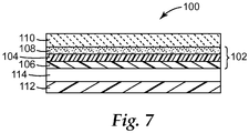
- the matrix comprising the nanoscale dispersed phase can be provided, for example, as a coating on a substrate.
- the substrate can be, for example, a polymeric substrate, a glass substrate or window, or a function device such as an organic light emitting diode (OLED), a display, a photovoltaic device, or the like.
- the matrix comprising the dispersed phase can be coated on the substrate and cured using methods known in the art such as, for example, casting cure by casting drum, die coating, flow coating, or dip coating.
- the coating can be prepared in any desired thickness greater than about 1 micron or preferably greater than about 4 microns.
- the coating can be cured by UV, electron beam, or heat.
- the matrix comprising the dispersed phase may be the article itself.
- the surface of the matrix comprising the nanoscale dispersed phase may be microstructured.
- a substrate with a v-groove microstructured surface can be coated with polymerizable matrix materials comprising a nanodispersed phase and treated by plasma etching to form nanostructures on v-groove microstructured surface.
- a microstructured article such as Fresnel lens or a microstructured article comprising microreplicated posts or columns comprising nanodispersed phases can be also treated by plasma etching to form nanostructures on microstructures.
- Other examples include a fine micro-structured surface resulting from controlling the solvent evaporation process from multi-solvent coating solutions, described as in U.S. Patent 7,378,136 ; or the structured surface from the micro-replication method disclosed in U.S. Patent 7,604,381 ; or any other structured surface induced by electrical and magnetic field or other means.
- the matrix is anisotropically etched using chemically reactive plasma.
- the RIE process for example, involves generating plasma under vacuum by an electromagnetic field. High energy ions from the plasma attack or etch away the matrix material.
- a typical RIE system consists of a vacuum chamber with two parallel electrodes, the "powered electrode” (or “sample carrier electrode”) and the counter-electrode, which create an electric field that accelerates ions toward.
- the powered electrode is situated in the bottom portion of the chamber and is electrically isolated from the rest of the chamber.
- the article or sample to be nanostructured is placed on the powered electrode.
- Reactive gas species can be added to the chamber, for example, through small inlets in the top of the chamber and can exit to the vacuum pump system at the bottom of the chamber.
- Plasma is formed in the system by applying a RF electromagnetic field to the powered electrode.
- the field is typically produced using a 13.56 MHz oscillator, although other RF sources and frequency ranges may be used.
- the gas molecules are broken and can become ionized in the plasma and accelerated toward the powered electrode to etch the sample.
- the large voltage difference causes the ions to be directed toward the powered electrode where they collide with the sample to be etched. Due to the mostly vertical delivery of the ions, the etch profile of the sample is substantially anisotropic.
- the powered electrode is smaller than the counter-electrode creating a large voltage potential across the ion sheath adjacent the powered electrode.
- the etching is to a depth greater than about 100nm.
- the process pressure is typically maintained at below about 2.7 Pa (20mTorr; preferably, below about 1.3 Pa (10mTorr)) but greater than about 0.1 Pa (1mTorr).
- This pressure range is very conducive for generation of the anisotropic nanostructure in a cost effective manner.
- the pressure is above about 2.7 Pa (20mTorr)
- the etching process becomes more isotropic because of the collisional quenching of the ion energy.
- the pressure goes below about 0.1 Pa (1mTorr)
- the etching rate becomes very low because of the decrease in number density of the reactive species.
- the gas pumping requirements become very high.
- the power density of the RF power of the etching process is preferably in the range of about 0.1 to about 1.0 watts/cm 3 (preferably, about 0.2 to about 0.3 watts/cm 3 ).
- the type and amount of gas utilized will depend upon the matrix material to be etched.
- the reactive gas species need to selectively etch the matrix material rather than the dispersed phase.
- Additional gases may be used for enhancing the etching rate of hydrocarbons or for the etching of non-hydrocarbon materials.
- fluorine containing gases such as perfluoromethane, perfluoroethane, perfluoropropane, sulfurhexafluoride, nitrogen trifluoride, and the like can be added to oxygen or introduced by themselves to etch materials such as SiO 2 , tungsten carbide, silicon nitride, amorphous silicon, and the like.
- Chlorine-containing gases can likewise be added for the etching of materials such as aluminum, sulfur, boron carbide, and semiconductors from the Group II-VI (including, but not limited to, cadmium, magnesium, zinc, sulfur, selenium, tellurium, and combinations thereof and from the Group III-V (including, but not limited to, aluminum, gallium, indium, arsenic, phosphorous, nitrogen, antimony, or combinations thereof.
- Hydrocarbon gases such as methane can be used for the etching of materials such as gallium arsenide, gallium, indium, and the like.
- Inert gases, particularly heavy gases such as argon can be added to enhance the anisotropic etching process.
- the method of the invention can also be carried out using a continuous roll-to-roll process.
- the method of the invention can be carried out using "cylindrical" RIE.
- Cylindrical RIE utilizes a rotating cylindrical electrode to provide anisotropically etched nanostructures on the surface of the articles of the invention.
- cylindrical RIE for making the nanostructured articles of the invention can be described as follows.
- a rotatable cylindrical electrode (“drum electrode") powered by radio-frequency (RF) and a grounded counter-electrode are provided inside a vacuum vessel.
- the counter-electrode can comprise the vacuum vessel itself.
- Gas comprising an etchant is fed into the vacuum vessel, and plasma is ignited and sustained between the drum electrode and the grounded counter-electrode. The conditions are selected so that sufficient ion bombardment is directed perpendicular to the circumference of the drum.
- a continuous article comprising the matrix containing the nanodispersed phase can then be wrapped around the circumference of the drum and the matrix can be etched in the direction normal to the plane of the article.
- the matrix can be in the form of a coating on an article such as, for example, on a film or web, or the matrix can be the article itself.
- the exposure time of the article can be controlled to obtain a predetermined etch depth of the resulting nanostructure.
- the process can be carried out at an operating pressure of approximately 1.3 Pa (10mTorr).
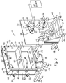
- FIGS. 1 and 2 illustrate a cylindrical RIE apparatus that is useful for the methods of the invention.
- a common element for plasma creation and ion acceleration is generally indicated as 10.
- This RIE apparatus 10 includes a support structure 12, a housing 14 including a front panel 16 of one or more doors 18, side walls 20 and a back plate 22 defining an inner chamber 24 therein divided into one or more compartments, a drum 26 rotatably affixed within the chamber, a plurality of reel mechanisms rotatably affixed within the chamber and referred to generally as 28, drive mechanism 37 for rotatably driving drum 26, idler rollers 32 rotatably affixed within the chamber, and vacuum pump 34 fluidly connected to the chamber.
- Support structure 12 is any means known in the art for supporting housing 14 in a desired configuration, a vertically upright manner in the present case.
- housing 14 can be a two-part housing as described below in more detail.
- support structure 12 includes cross supports 40 attached to each side of the two-part housing for supporting apparatus 10.
- cross supports 40 include both wheels 42 and adjustable feet 44 for moving and supporting, respectively, apparatus 10.
- cross supports 40 are attached to each side of housing 14 through attachment supports 46.
- cross supports 40 are connected to one of side wails 20, namely the bottom side wall, via attachment supports 46, while cross supports 40 on the other side of housing 14 are connected to back plate 22 by attachment supports 46.
- An additional crossbar 47 is supplied between cross supports 40 on the right-hand side of apparatus 10 as shown in FIG. 1 . This can provide additional structural reinforcement.
- Housing 14 can be any means of providing a controlled environment that is capable of evacuation, containment of gas introduced after evacuation, plasma creation from the gas, ion acceleration, and etching.
- housing 14 has outer walls that include front panel 16, four side walls 20, and a back plate 22.
- the outer walls define a box with a hollow interior, denoted as chamber 24.
- Side walls 20 and back plate 22 are fastened together, in any manner known in the art, to rigidly secure side walls 20 and back plate 22 to one another in a manner sufficient to allow for evacuation of chamber 24, containment of a fluid for plasma creation, plasma creation, ion acceleration, and etching.
- Front panel 16 is not fixedly secured so as to provide access to chamber 24 to load and unload substrate materials and to perform maintenance.
- Front panel 16 is divided into two plates connected via hinges 50 (or an equivalent connection means) to one of side walls 20 to define a pair of doors 18. These doors seal to the edge of side walls 20, preferably through the use of a vacuum seal (for example, an O-ring).
- Locking mechanisms 52 selectively secure doors 18 to side walls 20 and can be any mechanism capable of securing doors 18 to walls 20 in a manner allowing for evacuation of chamber 24, storage of a fluid for plasma creation, plasma creation, ion acceleration, and etching.
- chamber 24 is divided by a divider wall 54 into two compartments 56 and 58.
- a passage or hole 60 in wall 54 provides for passage of fluids or substrate between compartments.
- the chamber can be only one compartment or three or more compartments.
- the chamber is only one compartment.
- Housing 14 includes a plurality of view ports 62 with high pressure, clear polymeric plates 64 sealably covering ports 62 to allow for viewing of the etching process occurring therein. Housing 14 also includes a plurality of sensor ports 66 in which various sensors (for example, temperature, pressure, etc.) can be secured. Housing 14 further includes inlet ports 68 providing for conduit connection through which fluid can be introduced into chamber 24 as needed. Housing 14 also includes pump ports 70 and 72 that allow gases and liquids to be pumped or otherwise evacuated from chamber 24.
- Pump 34 is shown suspended from one of sides 20, preferably the bottom (as shown in FIG. 2 ).
- Pump 34 can be, for example, a turbo-molecular pump fluidly connected to the controlled environment within housing 14.
- Other pumps such as diffusion pumps or cryopumps, can be used to evacuate lower chamber 58 and to maintain operating pressure therein.
- the process pressure during the etching step is preferably chosen to be between about 0.1 Pa (1mTorr) and about 2.7 Pa (20mTorr) to provide anisotropic etching.
- Sliding valve 73 is positioned along this fluid connection and can selectively intersect or block fluid communication between pump 34 and the interior of housing 14. Sliding valve 73 is movable over pump port 62 so that pump port 62 can be fully open, partially open, or closed with respect to fluid communication with pump 34.
- Drum 26 preferably is a cylindrical electrode 80 with an annular surface 82 and two planar end surfaces 84.
- the electrode can be made of any electrically conductive material and preferably is a metal such as, for example, aluminum, copper, steel, stainless steel, silver, chromium or an alloy of any one or more of the foregoing.
- the electrode is aluminum, because of the ease of fabrication, low sputter yield, and low costs.
- Drum 26 is further constructed to include non-coated, conductive regions that allow an electric field to permeate outward as well as non-conductive, insulative regions for preventing electric field permeation and thus for limiting film coating to the non-insulated or conductive portions of the electrode.
- the electrically non-conductive material typically is an insulator, such as a polymer (for example, polytetrafluoroethylene).
- a polymer for example, polytetrafluoroethylene
- FIG. 1 shows an embodiment of drum 26 where annular surface 82 and end surfaces 84 of drum 26 are coated with an electrically non-conductive or insulative material, except for annular channel 90 in annular surface 82 which remains uncoated and thus electrically conductive.
- a pair of dark space shields 86 and 88 cover the insulative material on annular surface 82, and in some embodiments cover end surfaces 84.
- the insulative material limits the surface area of the electrode along which plasma creation and negative biasing may occur.
- dark space shields 86 and 88 can cover part or all of the insulated material.
- These dark space shields may be made from a metal such as aluminum but do not act as conductive agents because they are separated from the electrode by means of an insulating material (not shown). This allows confinement of the plasma to the electrode area.
- drum 26 includes a pair of insulative rings 85 and 87 affixed to annular surface 82 of drum 26.
- insulative ring 87 is a cap which acts to also cover end surface 84.
- Bolts 92 secure support means 94, embodied as a flat plate or strap, to back plate 22.
- Bolts 92 and support means 94 can assist in supporting the various parts of drum 26.
- the pair of insulative rings 85 and 87, once affixed to annular surface 82, define an exposed electrode portion embodied as channel 90.
- electrode 80 is covered in some manner by an insulative material in all areas except where the substrate contacts the electrode (that is, touching or within the plasma dark space limit of the electrode (for example, about 3mm)). This defines an exposed electrode portion that can be in intimate contact with the substrate. The remainder of the electrode is covered by an insulative material. When the electrode is powered and the electrode becomes negatively biased with respect to the resultant plasma, this relatively thick insulative material prevents etching on the surfaces it covers. As a result, etching is limited to the uncovered area (that is, that which is not covered with insulative material, channel 90), which preferably is covered by relatively thin substrate material.
- drum 26 is rotatably affixed to back plate 22 through a ferrofluidic feedthrough and rotary union 38 (or an equivalent mechanism) affixed within a hole in back plate 22.
- the ferrofluidic feedthrough and rotary union provide separate fluid and electrical connection from a standard coolant fluid conduit and electrical wire to hollow coolant passages and the conductive electrode, respectively, of rotatable drum 26 during rotation while retaining a vacuum seal.
- the rotary union also supplies the necessary force to rotate the drum, which force is supplied from any drive means such as a brushless DC servo motor.
- connection of drum 26 to back plate 22 and the conduit and wire may be performed by any means capable of supplying such a connection and is not limited to a ferrofluidic feedthrough and a rotary union.
- a ferrofluidic feedthrough and rotary union is a two-inch (about 5cm) inner diameter hollow shaft feedthrough made by Ferrofluidics Co. (Nashua, NH).
- Drum 26 is rotatably driven by drive assembly 37, which can be any mechanical and/or electrical system capable of translating rotational motion to drum 26.
- drive assembly 37 includes motor 33 with a drive shaft terminating in drive pulley 31 that is mechanically connected to a driven pulley 39 rigidly connected to drum 26.
- Belt 35 (or equivalent structure) translates rotational motion from drive pulley 31 to driven pulley 39.
- the plurality of reel mechanisms 28 are rotatably affixed to back plate 22.
- the plurality of reel mechanisms 28 includes a substrate reel mechanism with a pair of substrate spools 28A and 28B, and, in some embodiments, also can include a spacing web reel mechanism with a pair of spacing web spools 28C and 28D, and masking web reel mechanism with a pair of masking web spools 28E and 28F, where each pair includes one delivery and one take-up spool.
- at least each take-up reel 28B, 28D, and 28F includes a drive mechanism 27 mechanically connected thereto such as a standard motor as described below for supplying a rotational force that selectively rotates the reel as needed during etching.
- each delivery reel 28A, 28C, and 28E in select embodiments includes a tensioner for supplying tautness to the webs and/or a drive mechanism 29.
- Each reel mechanism includes a delivery and a take-up spool which may be in the same or a different compartment from each other, which in turn may or may not be the same compartment the electrode is in.
- Each spool is of a standard construction with an axial rod and a rim radially extending from each end defining a groove in which an elongated member, in this case a substrate or web, is wrapped or wound.
- Each spool is securably affixed to a rotatable stem sealably extending through back plate 22.
- the stem is mechanically connected to a motor 27 (for example, a brushless DC servo motor).
- the spool is merely coupled in a rotatable manner through a coupling 29 to back plate 22 and may include a tension mechanism to prevent slack.
- RIE apparatus 10 also includes idler rollers 32 rotatably affixed within the chamber and pump 34 fluidly connected to the chamber.
- the idler rollers guide the substrate from the substrate spool 28A to channel 90 on drum 26 and from channel 90 to take-up substrate spool 28B.
- idler rollers 32 guide these webs and the substrate from substrate spool 28A and masking web spool 28E to channel 90 and from channel 90 to take-up substrate spool 28B and take-up masking web spool 28F, respectively.
- RIE apparatus 10 further includes a temperature control system for supplying temperature controlling fluid to electrode 80 via ferrofluidic feedthrough 38.
- the temperature control system may be provided on apparatus 10 or alternatively may be provided from a separate system and pumped to apparatus 10 via conduits so long as the temperature control fluid is in fluid connection with passages within electrode 80.
- the temperature control system may heat or cool electrode 80 as is needed to supply an electrode of the proper temperature for etching.
- the temperature control system is a coolant system using a coolant such as, for example, water, ethylene glycol, chloro fluorocarbons, hydrofluoroethers, and liquefied gases (for example, liquid nitrogen).
- RIE apparatus 10 also includes an evacuation pump fluidly connected to evacuation port(s) 70.
- This pump may be any vacuum pump, such as a Roots blower, a turbo molecular pump, a diffusion pump, or a cryopump, capable of evacuating the chamber. In addition, this pump may be assisted or backed up by a mechanical pump.
- the evacuation pump may be provided on apparatus 10 or alternatively may be provided as a separate system and fluidly connected to the chamber.
- RIE apparatus 10 also includes a fluid feeder, preferably in the form of a mass flow controller that regulates the fluid used to create the thin film, the fluid being pumped into the chamber after evacuation thereof.
- the feeder may be provided on apparatus 10 or alternatively may be provided as a separate system and fluidly connected to the chamber.
- the feeder supplies fluid in the proper volumetric rate or mass flow rate to the chamber during etching.
- the etching gases can include, for example, oxygen, argon, chlorine, fluorine, carbon tetrafluoride, carbontetrachloride, perfluoromethane, perfluoroethane, perfluoropropane, nitrogen trifluoride, sulfur hexafluoride, methane, and the like. Mixtures of gases may be used advantageously to enhance the etching process.
- RIE apparatus 10 also includes a power source electrically connected to electrode 80 via electrical terminal 30.
- the power source may be provided on apparatus 10 or alternatively may be provided on a separate system and electrically connected to the electrode via electrical terminal (as shown in FIG. 2 ). In any case, the power source is any power generation or transmission system capable of supplying sufficient power. (See discussion infra.)
- RF power is preferred. This is because the frequency is high enough to form a self bias on an appropriately configured powered electrode but not high enough to create standing waves in the resulting plasma.
- RF power is scalable for high output (wide webs or substrates, rapid web speed).
- the negative bias on the electrode is a negative self bias, that is, no separate power source need be used to induce the negative bias on the electrode. Because RF power is preferred, the remainder of this discussion will focus exclusively thereon.
- the RF power source powers electrode 80 with a frequency in the range of 0.01 to 50MHz preferably 13.56MHz or any whole number (for example, 1, 2, or 3) multiple thereof.
- This RF power as supplied to electrode 80 creates a plasma from the gas within the chamber.
- the RF power source can be an RF generator such as a 13.56MHz oscillator connected to the electrode via a network that acts to match the impedance of the power supply with that of the transmission line (which is usually 50 ohms resistive) so as to effectively transmit RF power through a coaxial transmission line.
- the plasma Upon application of RF power to the electrode, the plasma is established. In an 15 RF plasma the powered electrode becomes negatively biased relative to the plasma. This bias is generally in the range of 500 to 1400 volts. This biasing causes ions within the plasma to accelerate toward electrode 80. Accelerating ions etch the article in contact with electrode 80 as is described in more detail below.
- a full spool of substrate upon which etching is desired is inserted over the stem as spool 28A. Access to these spools is provided through lower door 18 since, in FIGS. 1 and 2 , the spools are located in lower compartment 58 while etching occurs in upper compartment 56. In addition, an empty spool is fastened opposite the substrate holding spool as spool 28B so as to function as the take-up spool after etching has occurred.
- spacer web delivery and/or take-up spool can be provided as spools 28C and 28D (although the location of the spools in the particular locations shown in the figures is not critical).
- a masking web can be positioned on an input spool as spool 28E and an empty spool is positioned as a take-up spool as spool 28F.
- the substrate on which etching is to occur are woven or otherwise pulled through the system to the take-up reels.
- Spacer webs generally are not woven through the system and instead separate from the substrate just before this step and/or are provided just after this step.
- the substrate is specifically wrapped around electrode 80 in channel 90 thereby covering the exposed electrode portion.
- the substrate is sufficiently taut to remain in contact with the electrode and to move with the electrode as the electrode rotates so a length of substrate is always in contact with the electrode for etching. This allows the substrate to be etched in a continuous process from one end of a roll to the other.
- the substrate is in position for etching and lower door 18 is sealed closed.
- Chamber 24 is evacuated to remove all air and other impurities. Once an etchant gas mixture is pumped into the evacuated chamber, the apparatus is ready to begin the process of etching.
- the RF power source is activated to provide an RF electric field to electrode 80. This RF electric field causes the gas to become ionized, resulting in the formation of a plasma with ions therein. This is specifically produced using a 13.56 MHz oscillator, although other RF sources and frequency ranges may be used.
- a negative DC bias voltage is created on electrode 80 by continuing to power the electrode with RF power.
- This bias causes ions to accelerate toward non-insulated electrode portion 90 of electrode 80 (the remainder of the electrode is either insulated or shielded).
- the ions selectively etch the matrix material (versus the dispersed phase) in the length of substrate in contact with channel 90 of electrode 80 causing anisotropic etching of the matrix material of on that length of substrate.
- the take-up spools are driven so as to pull the substrate and any masking webs through the upper compartment 54 and over electrode 80 so that etching of the matrix occurs on any unmasked substrate portions in contact with annular channel 90.
- the substrate is thus pulled through the upper compartment continuously while a continuous RF field is placed on the electrode and sufficient reactive gas is present within the chamber.
- the result is a continuous etching on an elongated substrate, and substantially only on the substrate. Etching does not occur on the insulated portions of the electrode nor does etching occur elsewhere in the chamber.
- grounded dark space shields 86 and 88 can be used.
- Dark space shields 86 and 88 can be of any shape, size, and material that is conducive to the reduction of potential fouling.
- dark space shields 86 and 88 are metal rings that fit over drum 26 and the insulation thereon. Dark space shields 86 and 88 do not bias due to the insulative material that covers drum 26 in the areas where dark space shields 86 and 88 contact drum 26.
- the dark space shields in this ring-like embodiment further include tabs on each end thereof extending away from drum 26 in a non-annular manner. These tabs can assist in aligning the substrate within channel 90.
- the temperature control system pumps fluid through electrode 80 throughout the process to keep the electrode at a desired temperature.
- this involves cooling the electrode with a coolant as described above, although heating in some cases may be desirable.
- heat transfer from the plasma to the substrate is managed through this cooling system, thereby allowing the coating of temperature sensitive films such as polyethyleneterephthalate, polyethylene naphthalate, and the like.
- the spools can be removed from shafts supporting them on the wall.
- the substrate with the nanostructured article thereon is on spool 28B and is ready for use.
- the nanostructured article comprise additional layers.
- the article may comprise an additional fluorochemical layer to give the article improved water and/or oil repellency properties.
- the nanostructured surface may also be post treated (for example, with an additional plasma treatment). Plasma post treatments may include surface modification to change the chemical functional groups that might be present on the nanostructure or for the deposition of thin films that enhance the performance of the nanostructure. Surface modification can include the attachment of methyl, fluoride, hydroxyl, carbonyl, carboxyl, silanol, amine, or other functional groups.
- the deposited thin films can include fluorocarbons, glass-like, diamond-like, oxide, carbide, nitride, or other materials.
- the density of the surface functional groups is high due to the large surface area of the anisotropically etched nanostructured surface.
- amine functionality biological agents such as antibodies, proteins, enzymes, and the like can be easily grafted to the amine functional groups.
- silanol functionality silane chemistries can be easily applied to the nanostructured surface due to the high density of silanol groups.
- Antimicrobial, easy-clean, and anti-fouling surface treatments that are based on silane chemistry are commercially available. Antimicrobial treatments may include quaternary ammonium compounds with silane end group.
- Easy-clean compounds may include fluorocarbon treatments such as perfluoropolyether silane, hexafluoropropyleneoxide (HFPO) silane, and the like.
- Anti-fouling treatments may include polyethyleneglycol silane.
- these thin films may provide additional durability to the nanostructure or provide unique optical effects depending upon the refractive index of the thin film.
- Specific types of thin films may include diamond-like carbon (DLC), diamond-like glass (DLG), amorphous silicon, silicon nitride, plasma polymerized silicone oil, aluminum, copper, and the like.
- the nanostructured articles of the invention can exhibit one or more desirable properties such as antireflective properties, light absorbing properties, antifogging properties, improved adhesion and durability.
- the surface reflectivity of the nanostructured anisotropic surface is about 50% or less than the surface reflectivity of an untreated surface.
- untreated surface means the surface of an article comprising the same matrix material and the same nanodispersed phase (as the nanostructured surface of the invention to which it is being compared) but without a nanostructured anisotropic surface.
- the percent reflection of the nanostructured anisotropic surface is less than 2%, preferably, less than 1%, and most preferable less than 0.5%, as measured using the "Measurement of Average % Reflection" method described in the Example section below.
- the percent transmission of the nanostructured anisotropic surface is about 2% or more than the percent transmission of an untreated surface as measured using the "Measurement of Average % Transmission" method described in the Example section below.
- the nanostructured anisotropic surface has a water contact angle of less than about 20° (preferably, less than about 15°; more preferably less than about 10°) as measured using the "Water Contact Angle Measurement" method described in the Example section below.
- the nanostructured anisotropic surface absorbs about 2% or more light than an untreated surface.
- the nanostructured anisotropic surface has a pencil hardness greater than about 2H (preferably, greater than about 4H) as determined according to ASTM D-3363-05.
- Some embodiments of the invention further comprise a layer or coating comprising, for example, ink, encapsulant, adhesive, or metal attached to the nanostructured anisotropic surface.
- the layer or coating can have improved adhesion to the nanostructured anisotropic surface of the invention than to an untreated surface.
- the nanostructured articles of the invention are useful for numerous applications including, for example, display applications (for example, liquid crystal displays (LCD), light emitting diode (LED) displays, or plasma displays); light extraction; electromagnetic interference (EMI) shielding, ophthalmic lenses; face shielding lenses or films; window films; antireflection for construction applications, construction applications or traffic signs; and the like.
- display applications for example, liquid crystal displays (LCD), light emitting diode (LED) displays, or plasma displays
- EMI electromagnetic interference
- ophthalmic lenses face shielding lenses or films
- window films antireflection for construction applications, construction applications or traffic signs; and the like.
- the nanostructured articles of the invention are also useful for solar applications such as solar films and Fresnel lenses.
- They can be used as the front surface of solar thermal hot liquid/air heat panels or any solar energy absorbing device; for solar thermal absorbing surfaces having micro- or macro-columns with additional nanoscale surface structure; for the front surface of flexible solar photovoltaic cells made with amorphous silica photovoltaic cells or CIGS photovoltaic cells; and for the front surface of a film applied on top of flexible photovoltaic cells.
- FIG. 7 shows a schematic cross sectional view of an exemplary display 100, such as a LCD, using an antireflective (AR) article as disclosed herein.
- a composite 102 includes a substrate 104 having opposing first and second surfaces with an AR layer 106 disposed on the first surface of the substrate and an optically clear adhesive (OCA) 108 disposed on the second surface of the substrate.
- OCA optically clear adhesive
- a release liner (not shown) can be used to protect the OCA and a premask (also not shown) can be used to protect the AR coating during processing and storage.
- the composite 102 is then laminated to a glass or polarizer substrate 110 such that the OCA is in direct contact with the glass substrate which is then assembled to a liquid crystal module 112, typically, with an air gap 114 disposed between the AR coating and the liquid crystal module.
- a glass or polarizer substrate 110 such that the OCA is in direct contact with the glass substrate which is then assembled to a liquid crystal module 112, typically, with an air gap 114 disposed between the AR coating and the liquid crystal module.
- Suitable substrate for use in this present disclosure and particularly for display applications include any material that is at least 90% transmissible in visible light (400 to 800nm wavelength) and has a haze of less than about 5%.
- Illustrative examples of polymeric substrates include polycarbonate, poly(meth)acrylate, polyester, nylon, siloxane, fluoropolymer, urethane, epoxy, cyclic olefin copolymer, triacetate cellulose, diacrylate cellulose or blends or copolymers thereof, styrene based polymers such as polystyrene, acrylonitrile-styrene copolymer, and olefin based polymers.
- the substrate has a thickness of up to 250 micrometer ( ⁇ m).
- the substrate can contain a cross-linkable material selected from multi(meth)acrylate, polyester, epoxy, fluoropolymer, urethane, siloxane and blends and copolymers thereof.
- the OCAs that may be used in the present disclosure are those that exhibit an optical transmission of at least about 90%, or even higher, and a haze value of below about 5% or even lower, as measured on a 25 ⁇ m thick sample in the matter described below in the Example section under the Haze and Transmission Testing for OCA.
- Suitable OCAs may have antistatic properties, may be compatible with corrosion sensitive layers, may be able to be released from the glass substrate by stretching the adhesive.
- Illustrative OCAs include those described in publication WO 2008/128073 relating to antistatic optically clear pressure sensitive adhesive, U.S. Patent Application Publications U.S. 2009/030084 A1 relating to stretch releasing OCA and U.S.
- the OCA has a thickness of about 5 ⁇ m or less.
- the hardcoat provided in liquid form, is coated on to a first surface of the substrate.
- the liquid is cured or dried to form a dry AR layer on the substrate.
- the hardcoated substrate is then processed through the reactive ion etching (RIE) process described above using, in one exemplary method, the apparatus described in FIG. 1 .
- RIE reactive ion etching
- the RIE process also minimizes the undesirable phenomenon of iridescence (also referred to as "interference fringes").
- the difference between the refractive index of the substrate and the hardcoat layer can cause the phenomenon of iridescence, which occurs when external light incident on the hardcoat layer is reflected to produce rainbow-like colors.
- the iridescence is highly undesirable in a display application as it will obstruct the image on the display.
- the RIE process can reduce the reflection from the air-front surface interface of the substrate coated with nanoparticle filled hardcoat, which in turn reduces the iridescence to achieve a layer exhibiting excellent antireflective properties and minimal iridescence.
- nanoparticles such as ZrO 2 can be used to tune the refractive index of coating matrix of the hardcoat to substantially match that of the substrate.
- the nanodispersed phase can be etched away using plasma to form a nanostructured (or nanoporous) surface.
- This method can be carried out using planar RIE or cylindrical RIE essentially as described above, but using etching selectivity to favor etching the nanodispersed phase rather than the matrix (that is, by selecting gases that etch dispersed phase material rather than the matrix material).
- the anisotropic nanostructures of this invention were obtained by using the plasma treatment system described in U.S. Patent No. 5,888,594 (David et al. ) with some modifications.
- the width of the drum electrode was increased to 14.5 (36.8cm) and the separation between the two compartments within the plasma system was removed so that all the pumping was carried out by means of the turbo-molecular pump and thus operating at a much lower operating pressure than is conventionally done with plasma processing.
- the average % reflection (%R) of the plasma treated surface was measured using PerkinElmer Lambda 950 UV-VIS-NIR Scanning Spectrophotometer.
- One sample of each film was prepared by applying Yamato Black Vinyl Tape #200-38 (obtained from Yamato International Corporation, Woodhaven, MI) to the backside of the sample.
- Yamato Black Vinyl Tape #200-38 obtained from Yamato International Corporation, Woodhaven, MI
- Clear poly (methyl methacrylate) (PMMA) film of which transmission and reflection from both sides were predetermined was utilized to establish the % reflection from the black tape.
- the black tape was laminated to the backside of the sample using a roller to ensure there were no air bubbles trapped between the black tape and the sample.
- the sample was placed in the machine so that the non-tape side was against the aperture.
- the % reflection was measured at an 8° incident angle and average % reflection was calculated by subtracting the % reflection of the black tape for the wavelength range of 400-800nm.
- the average % transmission was measured with an internally built machine.
- the machine uses a quartz tungsten halogen (QTH) lamp powered with a stabilized source and a custom 4" (10.2cm) SpectralonTM sphere as a light source to measure sample transmission using a D/0 geometry.
- QTH quartz tungsten halogen
- SpectralonTM sphere as a light source to measure sample transmission using a D/0 geometry.
- NIR near infrared
- a simple spectrograph with a Czerny-Turner optical layout and a single grating is used for light dispersal onto each detector.
- Water contact angle was measured with a static contact angle measurement device.
- the machine is equipped with a digital camera, automatic liquid dispensers, and sample stages allowing hands-free contact angle via automated placement of a drop of water.
- the drop shape is captured automatically and then analyzed via Drop Shape Analysis by a computer to determine the static contact angle.
- a 25 micron thick sample of the OC adhesive was laminated to a 25 micron thick Melinex ® polyester film 454 (from DuPont Company, Wilmington, DE) in a manner so as to assure that no air bubbles are trapped between the film and the adhesive layer.
- a 75mm by 50mm plain micro slide (a glass slide from Dow Corning, Midland, MI), that had been wiped three times with isopropanol, was laminated to the adhesive sample using a hand roller to assure no air bubbles were trapped between the adhesive and the glass slide.
- the percent (%) transmission and haze were measured using a Model 9970 BYK Gardner TCS Plus Spectrophotometer (from BYK Gardner, Columbia, MD). The background measurement was made with a sandwich of the Melinex ® polyester film 454 and the glass slide. The % transmission and the haze of the adhesive sample were then obtained directly on the film/adhesive/glass laminate in the spectrophotometer.
- 40 wt% of 20 nm silica particles filled acrylic coating was prepared from Nalco 2327, SR444 (pentaerythritol triacylate), A-174 (methacryloxypropyltrimethoxy silane), and IrgacureTM 184 (photoinitiator) according to the method described in U.S. Patent No. 5,104,929 (Bilkadi ).
- the coating formulation was then diluted with isopropyl alcohol (IPA) to form 50 wt% solution.
- IPA isopropyl alcohol
- the coating solution was then coated onto primed 2 mil PET film.
- the solution was syringe-pumped into a coating die, and the coating was dried by passing through an oven set at 120°C and then cured by a UV source.
- the resulting cured coating was approximately 4 microns thick.
- the samples were treated by oxygen plasma with different treatment times (30, 60, 90, 120, 150, and 180 seconds). The average % reflection was measured and reported in Table 1. Significant reduction in reflection was obtained for Samples 2-7 and 90 seconds treatment provided the best reflection behavior.
- Table 1 Reflection results of plasma treated samples of Example 1 Sample 1 2 3 4 5 6 7 O 2 plasma treatment time (seconds) 0 (control) 30 60 90 120 150 180 Average % R (400-800 nm) 4.58 1.42 1.18 1.04 1.36 1.69 1.95
- SR295 penentaerythritol tetraacrylate
- SR238 hexane diol diacrylate
- SR506 isobornyl acrylate
- 5nm silica particle Nalco 2326 400gm was charged to a 1qt jar.
- 1-methoxy-2-propanol 450gm
- 3-(Methacryloyloxy)propyltrimethoxy silane 27.82gm
- Prostab 5128 hindere amine nitroxide inhibitor
- the jar was sealed and heated to 80°C for 16hr.
- the surface modified silica dispersion (1166 gm), resin mixture (70gm) of SR295, SR238 and SR506, and 5% Prostab in water (058gm) were combined and mixed.
- the water and 1-methoxy-2-propanol were removed from the mixture via rotary evaporation. This yielded a clear composition (184.6gm) of SiO 2 resin mixture.
- the weight percent of modified silica in the formulation was about 60 wt%.
- Preparation of 20nm silica particle concentrate was done with the same procedure by replacing Nalco 2326 with Nalco 2327.
- the nanoparticles filled resins were diluted with the mixture of SR295, SR238, and SR506 for various concentrations of silica nanoparticles in the acrylic hardcoat formulations.
- the hardcoats were then applied to primed 5 mil PET film with two different particle sizes (5nm and 20nm) and various concentrations (10%, 20%, 40% and 50% by weight) of silica nanoparticles in the acrylic coating mixture according to Table 2.
- One-side plasma treatment was then done under various web speeds (10, 5, 3.3, 2.5, 1.7 and 1.3 feet/min) corresponding to different treatment times (30, 60, 90, 120, 150 and 180 seconds).
- Table 2 Transmission results of plasma treated samples of Example 2 Ave % Transmission from 400-800nm before RIE After RIE O2 C3F8-O2 Ar-O2 (etching time, sec) (etching time, sec) (etching time, sec) Samples 5nm SiO2 (wt%) 20nm SiO2 (wt%) 30 60 90 120 150 180 30 60 90 120 150 180 30 60 90 120 150 180 8 49.75 0 90.0 91.0 91.5 92.0 92.2 92.6 92.8 90.5 90.8 91.0 91.3 91.6 91.7 90.8 91.3 91.9 92.2 92.6 92.2 9 39.8 0 89.9 91.3 92.2 92.7 92.9 93.1 92.9 90.7 91.2 91.6 91.9 92.2 92.4 91.1 92.0 92.7 92.8 92.9 93.1 10 19.9 0 89.8 92.2 92.9 93.1 93.1
- Table 4 Reflection results of plasma treated samples of Example 3 Sample Formulation (wt %) O2 plasma treatment time (seconds) Average %R (400-800 nm) CN991 CN991/CN2303 (70:30) THFA MA0736 TPO-L 16 0 88 10 0 2 90 3.37 17 0 87 10 1 2 90 2.89 18 0 85 10 3 2 90 2.65 19 0 83 10 5 2 90 2.03 20 0 81 10 7 2 90 1.44 21 0 78 10 10 2 90 1.01 22 0 73 10 15 2 90 0.9 23 0 68 10 20 2 90 0.73
- ImpermTM 103 is nylon MXD6 comprising 3 wt% nano-scale talc and commercially available from Nanocor Inc. Film sample was prepared from Imperm 103 by melt extrusion process through a slot die and then treated by Ar-O2 plasma corresponding to different treatment times (30, 60, and 90 seconds). The % reflection was then measured and reported in Table 5. Table 5: Reflection results of plasma treated samples of Example 4 Sample 24 25 26 27 Ar-O2 plasma treatment time (seconds) 0 (Imperm 103 control) 30 60 90 Average %R (400-800 nm) 5.12 4.25 2.05 0.95
- Sample #5 in Example 1 was further treated by applying a perfluoropolyether-silane (EGC-1720 available from 3M Company) solution to the etched surface.
- EGC-1720 available from 3M Company
- the static contact angle and transmission for Sample #1, Sample #5, and Sample #5 treated with EGC-1720 were measured. The results are reported in Table 6 below.
- the contact angle to water is shown to be adjustable from below 10 degrees to above 120 degrees.
- Table 6 Transmission and water contact test results of the samples in Example 5 Sample Comment Average % transmission (400-800 nm) H2O contact angle (degree) 1 PET coated with coating from Example 1 (Sample #1 in Example 1) 90.5 71.8 5 Sample #5 in Example 1 93.5 9.8 28 Sample #5 treated with EGC-1720 94.1 122.5
- a substrate web containing microstructure (Brightness Enhancement Film-BEF made from 37wt% 20nm silica particles filled coating in U.S. Patent Application Publication 20080050560-A1 ) was used to generate a nanostructure on top of the microstructure by plasma treatment.
- oxygen gas was used with a treatment time of 90 seconds with the flow rate, pressure and power maintained at 500sccm, 1 Pa (8mTorr) and 2000 watts respectively.
- the percent reflection was measured.
- the average % reflection in the wavelength range of 400-800nm is reduced from 2.2% to 1%, a 50% reduction in the surface reflection.
- Example 2 Two of the plasma etched samples of Example 2 above (10wt% concentration of 20nm silica particles etched at 60 and 180 seconds) were characterized by cross-sectional high resolution scanning electron microscope (HRSEM). The results are depicted in FIG. 5 (5 feet/min) and 6 (1.3 feet/min). It is clear that the etching is anisotropic in the sub 100nm range. Several holes and pillars that are in the 10-50nm diameter range are in the order of 500 nanometers range for depth, leading to a 5:1 aspect ratio or greater.
- HRSEM high resolution scanning electron microscope
- the hole marked as "A” in Figure 6 has a diameter of 27 nanometers and a depth of 480 nanometers while the pillar marked as "B” has a diameter of 18 nanometers and a depth of 364 nanometers.
- the corresponding aspect ratio of these structures approaches about 20:1.
- a flexible solar absorbing sheet was prepared with an extrusion replication process and subsequently treated with plasma etching of the structured surface.
- Carbon filled thermoplastic polyurethane (URC7000-TC-1 available from PolyOne Corp, Cleveland, OH) was melted with an extruder and formed through an extrusion sheet die onto a casting roll perforated with an array of holes distanced about 3mm apart with depths of 0.5cm and diameters of 2mm.
- the extruder had a diameter of about 3.2cm, a screw speed of 80 rpm, and a rising temperature profile from 100°C to 250°C.
- the extrusion replication casting roll was the center roll of a 3 roll stack with a nip roll capable of pushing the carbon filled polymer melt into the casting replication tool roll at a pressure of 0.24MPa.
- the extrusion replication casting process was operated at a speed of 0.61 meters/minute.
- Total thickness of the extrusion replicated cast sheet was 1.1cm with 1.0cm high posts or columns and 0.1cm thickness of continuous base film.
- % Reflection of this opaque columnar structured sheet was then measured to be 3.1% with a Lambda 950 spectraphotometer. Since the opaque structured sheet had no measurable light transmission, %Absorption was calculated to be 1-%R or 96.9% absorption.
- the flexible solar absorbing sheet was then treated by plasma in an O 2 -C 3 F 8 atmosphere for 60 seconds.
- % Reflection of the plasma etched opaque columnar structured sheet was measured to 1.4% with a Lambda 950 spectraphotomer demonstrating a 55% reduction in surface reflections.
- % Absorption of the plasma etched columnar-structured solar absorption sheet was calculated to be 98.6%.
- An article of this invention was prepared according to Example 1, Sample 5, using oxygen plasma and an etching time of 120 seconds.
- the adhesion of the anisotropically etched random nanostructure was measured against two different types of adhesives, a premium silicon adhesive and an "extra strength" acrylic adhesive.
- an unetched sample of the hardcoated substrate as in Example 1 was used.
- a 180 degree peel tester was used to test the adhesion strength.
- Test samples were cut into approximately 2-inch (5.1cm) wide x 6-inch (15.2cm) long strip and two different types of tapes having the two different adhesive types were used.
- the silicone adhesive tape is a 1-inch (2.5cm) wide ScotchTM Tape No. 8403 with a silicone adhesive and the acrylic adhesive tape is an "Extra Strength" 3 ⁇ 4-inch (1.9cm) wide ScotchTM Crystal Clear tape having a product number 34-8505-5627-4, available from 3M Company (St. Paul, MN).
- the adhesive tape was attached to the test samples by rolling a 4-inch (10.2cm) diameter roller having a weight of 450 grams onto the tape/sample sandwich. Peel measurements were taken at a speed of 12 inches/min (30.5cm/min) over a test length of 0.5 inches (1.3cm) and the average peel value over this distance was measured. Six different measurements were made for each type of sample/adhesive combination and summarized in Table 7. The average and standard deviation of the six measurements are also shown in this table. Table 7: Peel Measurements from Example 9 Sample No.
- Pencil hardness test according to ASTM D-3363-05 test method was utilized to evaluate the surface hardness of Sample 4 in Example 1.
- a complete set of pencil gradings starts with the hardest - 9H, 8H, 7H, 6H, 5H, 4H, 3H, 2H, F, HB, B, 2B, 3B, 4B, 5B, 6B, 7B, 8B, and 9B (the latter is the softest pencil).
- a pencil is used to make a line about one inch long on the sample. If the pencil leaves a visible scratch on the surface, then take the next soft pencil to repeat the test. The number of the first pencil that does not leave a visible mark is considered the "pencil hardness" rating of the surface.
- Sample 4 in Example 1 was found to be 4H by this test method
- Example 2 illustrates the use of an antireflective layer made according to Example 2 incorporated into a LCD.
- the hardcoat of Example 2 with 5nm silica naoparticle was coated at 10% by weight on to a first surface of a 2 mil PET film, which was previously primed.
- the dried hardcoated PET film was subjected to one-sided plasma treatment using a gas mixture of 25% argon, 75% oxygen with a treatment time of 60 seconds to yield an AR film.
- Table 8 below reports the data for 3 samples of Example 11 compared to 3 samples of Control ("Untreated" hardcoated PET).
- This example illustrates the situation where the hardcoat composition is made such that it substantially matches the refractive index of the substrate.
- the hardcoat solution is made by blending ZrO 2 naoparticles made according to U.S. Patent Nos. 6,376,590 and 7,241,437 dispersed in a polyacrylate matrix on to a first surface of a 5 mil PET film, which was previously primed.
- the solution was syringe-pumped into a coating die, and the coating was dried by passing through an oven set at 120°C and then cured by a UV source. The resulting cured coating was approximately 4 microns thick.
- the dried hardcoated PET film was subjected to one-sided plasma treatment using a gas mixture of 25% argon, 75% oxygen with a treatment time of 90 seconds to yield an AR film. Table 9 below reports the data for 3 samples of this example compared to 3 samples of "Untreated" hardcoated PET.
- An OC adhesive such as product number 8171, commercially available from 3M Company, was laminated to a second surface of the 5 mil PET film, i.e., on the side opposite of the hardcoat using a hand laminator to yield a composite.
- This composite was then laminated to a glass substrate and assembled with a liquid crystal module to yield a liquid crystal display that can be used for MHH device.
- the refractive index (N D ) of the glass was 1.52
- of the OC adhesive was 1.50
- of the PET substrate was 1.57
- of the AR layer was 1.57.
- Tables 8 and 9 shows transmission data of samples of Examples 11 and 12 of the present disclosure compared to samples of the untreated hardcoated PET. There is about a 3% gain in transmission after the hardcoated PET has been processed plasma treated through the reactive ion etching process, which is a significant increase for display applications. Such increase in transmission allows for lower power consumption by the display device as less battery power is needed to light the MHH device.
- Surface modified silica particles (20 nm) were prepared from Nalco 2327, A-174 (methacryloxypropyltrimethoxy silane), and 1-methoxy-2-propanol according to the method described in U.S. Patent No. 5,104,929 (Bilkadi ) to form 43.4 wt% A-174 functionalized silica particles in 1-methoxy-2-propanol.
- the material was coated on to a 0.005 inch primed PET film using a Meyer rod (#8 bar) coating device.
- the coated PET film was dried at room temperature inside a ventilated hood for 15 minutes.
- the coated film was cured using a UV processor equipped with a D-Bulb under a nitrogen atmosphere.
- the sample was then treated by oxygen plasma for 90 seconds. After plasma treatment, the average % reflection was 0.61% which is significantly lower than the value for the untreated film having an average percent reflection of 4.72%.
Claims (19)
- Composite comprenant :(a) un substrat ayant au moins 90 % de transmission en lumière visible et moins de 5 % de trouble, le substrat ayant des première et deuxième surfaces opposées ;(b) un article nanostructuré disposé sur la première surface du substrat, l'article nanostructuré comprenant une matrice et une phase dispersée à l'échelle nanométrique comprenant des nanoparticules, et ayant une surface anisotrope nanostructurée aléatoire, la surface anisotrope nanostructurée aléatoire comprenant des aspérités structurales ayant un rapport de hauteur à largeur de 1,5:1 ou plus élevé, dans lequel les nanoparticules ont un diamètre moyen dans la plage de 1 à 100 nanomètres ;
et(c) un adhésif optiquement transparent disposé sur la deuxième surface du substrat, l'adhésif optiquement transparent ayant au moins 90 % de transmission en lumière visible et moins de 5 % de trouble. - Affichage pour application électronique comprenant le composite selon la revendication 1, stratifié à un substrat de verre de telle sorte que l'adhésif optiquement transparent vient en contact avec le substrat de verre, ou un polariseur et l'assemblage des stratifiés avec un module d'affichage liquide.
- Composite selon la revendication 1, dans lequel la matrice comprend un revêtement dur comprenant des nanoparticules de SiO2, ZrO2 et de combinaisons de ceux-ci, dispersées dans une matrice réticulable comprenant un multi(méth)acrylate, du polyester, de l'époxy, un fluoropolymère, de l'uréthane, du siloxane, ou des mélanges ou copolymères de ceux-ci.
- Composite selon la revendication 1, dans lequel la phase dispersée à l'échelle nanométrique comprend des nanoparticules de SiO2, ZrO2, TiO2, ZnO, Al2O3, carbonate de calcium, silicate de magnésium, oxyde d'indium et d'étain, oxyde d'antimoine et d'étain, poly(tétrafluoroéthylène), carbone et de combinaisons de ceux-ci.
- Composite selon la revendication 1, dans lequel les nanoparticules sont modifiées en surface.
- Composite selon la revendication 1, dans lequel la matrice comprend un polymère choisi dans le groupe constitué de polycarbonate, poly(méth)acrylate, polyester, nylon, siloxane, fluoropolymère, uréthane, époxy, copolymère oléfinique cyclique, cellulose triacétate, cellulose diacrylate ou des mélanges ou copolymères de ceux-ci.
- Composite selon la revendication 1, dans lequel la matrice comprend un matériau inorganique choisi parmi le groupe d'oxyde de silicium et de carbure de tungstène.
- Composite selon la revendication 1, dans lequel le substrat comprend un matériau réticulable choisi parmi multi(méth)acrylate, polyester, époxy, fluoropolymère, uréthane, siloxane, ou des mélanges ou copolymères de ceux-ci.
- Composite selon la revendication 1, dans lequel le substrat comprend un polymère choisi dans le groupe constitué de polycarbonate, poly(méth)acrylate, polyester, nylon, siloxane, fluoropolymère, uréthane, époxy, copolymère oléfinique cyclique, cellulose triacétate, cellulose diacrylate ou des mélanges ou copolymères de ceux-ci.
- Composite selon la revendication 1, dans lequel le substrat comprend un verre ou un polariseur.
- Composite selon la revendication 1, dans lequel la matrice comprend un alliage ou une solution solide.
- Composite selon la revendication 1, dans lequel la concentration de la phase dispersée au sein de la matrice est comprise entre environ 5 et 90 pour cent en poids.
- Composite selon la revendication 1, dans lequel l'article nanostructuré comprend une surface microstructurée sur laquelle se trouve la surface anisotrope nanostructurée.
- Procédé de fabrication d'un composite, comprenant :(a) la fourniture d'un substrat ayant au moins 90 % de transmission en lumière visible et moins de 5 % de trouble ;(b) le revêtement d'une composition de revêtement dur sur la première surface principale du substrat pour donner une couche antiréfléchissante, la composition de revêtement dur comprenant des nanoparticules de SiO2, ZrO2 et de combinaisons de ceux-ci, les nanoparticules étant dispersées dans une matrice ;(c) le séchage de la solution de revêtement dur pour donner une couche antiréfléchissante ;(d) l'exposition de la couche antiréfléchissante à une attaque chimique ionique réactive comprenant les étapes de(i) mise en place de la couche antiréfléchissante sur une électrode cylindrique dans un récipient sous vide,(ii) introduction d'un gaz d'attaque chimique dans le récipient à une pression prédéfinie,(iii) production d'un plasma entre l'électrode cylindrique et une contre-électrode ;(iv) rotation de l'électrode cylindrique pour déplacer par translation le substrat ; et(v) attaque chimique anisotrope de la composition de revêtement dur ; et(e) la stratification d'un adhésif optiquement transparent disposé sur la deuxième surface du substrat, l'adhésif optiquement transparent ayant au moins 90 % de transmission en lumière visible et moins de 5 % de trouble.
- Procédé selon la revendication 14, dans lequel le plasma est un plasma d'oxygène.
- Procédé selon la revendication 14, dans lequel, à l'étape (d)(ii), l'agent d'attaque chimique est introduit à une pression d'environ 0,1 Pa à 2,7 Pa.
- Procédé selon la revendication 14, comprenant en outre l'étape de durcissement du revêtement dur lorsqu'il est sec pour donner une couche antiréfléchissante.
- Procédé selon la revendication 14, dans lequel le revêtement dur comprend des nanoparticules de SiO2, ZrO2 et des combinaisons de ceux-ci, dispersées dans une matrice réticulable comprenant du multi(méth)acrylate, du polyester, de l'époxy, du fluoropolymère, de l'uréthane, du siloxane, ou des mélanges ou copolymères de ceux-ci.
- Procédé selon la revendication 14, comprenant en outre la stratification du composite à un substrat de verre ou de polariseur.
Applications Claiming Priority (4)
| Application Number | Priority Date | Filing Date | Title |
|---|---|---|---|
| US14151708P | 2008-12-30 | 2008-12-30 | |
| US15768309P | 2009-03-05 | 2009-03-05 | |
| US23478209P | 2009-08-18 | 2009-08-18 | |
| PCT/US2009/068639 WO2010078071A1 (fr) | 2008-12-30 | 2009-12-18 | Articles antireflet et leurs procédés de fabrication |
Publications (2)
| Publication Number | Publication Date |
|---|---|
| EP2380045A1 EP2380045A1 (fr) | 2011-10-26 |
| EP2380045B1 true EP2380045B1 (fr) | 2017-06-28 |
Family
ID=42060629
Family Applications (1)
| Application Number | Title | Priority Date | Filing Date |
|---|---|---|---|
| EP09808972.5A Not-in-force EP2380045B1 (fr) | 2008-12-30 | 2009-12-18 | Articles antireflet et leurs procédés de fabrication |
Country Status (8)
| Country | Link |
|---|---|
| US (2) | US9435916B2 (fr) |
| EP (1) | EP2380045B1 (fr) |
| JP (2) | JP6174300B2 (fr) |
| KR (2) | KR101915868B1 (fr) |
| CN (1) | CN102326099B (fr) |
| SG (1) | SG172204A1 (fr) |
| TW (1) | TWI575249B (fr) |
| WO (1) | WO2010078071A1 (fr) |
Cited By (1)
| Publication number | Priority date | Publication date | Assignee | Title |
|---|---|---|---|---|
| CN109985782A (zh) * | 2019-04-10 | 2019-07-09 | 贵州钢绳股份有限公司 | 一种利用冷镀锌工艺在拉丝机卷筒内壁进行防锈处理的方法 |
Families Citing this family (71)
| Publication number | Priority date | Publication date | Assignee | Title |
|---|---|---|---|---|
| DE102006002713A1 (de) * | 2005-03-18 | 2006-10-12 | BSH Bosch und Siemens Hausgeräte GmbH | Frontbaugruppe für eine Wäschetrockenmaschine |
| US20100003493A1 (en) * | 2007-10-10 | 2010-01-07 | Ppg Industries Ohio, Inc. | Radiation curable coating compositions, related coatings and methods |
| KR101915868B1 (ko) | 2008-12-30 | 2018-11-06 | 쓰리엠 이노베이티브 프로퍼티즈 컴파니 | 반사방지 용품 및 이의 제조 방법 |
| WO2010123528A2 (fr) | 2008-12-30 | 2010-10-28 | 3M Innovative Properties Company | Articles nanostructurés et procédés de fabrication d'articles nanostructurés |
| US8553333B2 (en) * | 2009-01-23 | 2013-10-08 | State Of Oregon Acting By And Through The State Board Of Higher Education On Behalf Of Oregon State University | Nanostructured anti-reflective coatings for substrates |
| DE102009035797A1 (de) * | 2009-07-31 | 2011-02-03 | Leibniz-Institut Für Neue Materialien Gemeinnützige Gmbh | Verfahren zur Herstellung von Beschichtungen mit Antireflexionseigenschaften |
| EP2542617A1 (fr) * | 2010-03-03 | 2013-01-09 | 3M Innovative Properties Company | Polariseur revêtu à surface nanostructurée et son procédé de fabrication |
| TW201212972A (en) * | 2010-09-17 | 2012-04-01 | Univ Nat Yang Ming | A small ultraviolet (UV) irradiating module |
| US8469551B2 (en) * | 2010-10-20 | 2013-06-25 | 3M Innovative Properties Company | Light extraction films for increasing pixelated OLED output with reduced blur |
| JP5579020B2 (ja) * | 2010-10-27 | 2014-08-27 | 三菱樹脂株式会社 | 塗布層を有するポリエステルフィルム |
| US9310527B2 (en) | 2011-03-09 | 2016-04-12 | 3M Innovative Properties Company | Antireflective film comprising large particle size fumed silica |
| JP6014057B2 (ja) * | 2011-03-14 | 2016-10-25 | スリーエム イノベイティブ プロパティズ カンパニー | 多層のナノ構造化物品 |
| WO2012125324A1 (fr) * | 2011-03-14 | 2012-09-20 | 3M Innovative Properties Company | Articles nano-structurés |
| CN102749666B (zh) * | 2011-04-20 | 2015-04-01 | 国家纳米科学中心 | 一种减反射涂层的制备方法 |
| CN102841397B (zh) * | 2011-06-21 | 2016-06-15 | 宏腾光电股份有限公司 | 多层膜反射片及其制作方法 |
| EP2944671A1 (fr) * | 2011-08-17 | 2015-11-18 | 3M Innovative Properties Company of 3M Center | Articles nanostructurés et procédés pour les fabriquer |
| KR20130027852A (ko) * | 2011-09-08 | 2013-03-18 | 씨제이제일제당 (주) | 나노구조의 소수성 표면을 갖는 식품용기 및 그의 제조방법 |
| US9484123B2 (en) | 2011-09-16 | 2016-11-01 | Prc-Desoto International, Inc. | Conductive sealant compositions |
| JP2014534289A (ja) * | 2011-10-06 | 2014-12-18 | ソルヴェイ(ソシエテ アノニム) | コーティング組成物およびそれから製造される反射防止コーティング |
| WO2013106629A2 (fr) * | 2012-01-13 | 2013-07-18 | Corning Incorporated | Articles en verre résistant à la réflexion et leurs procédés de fabrication et d'utilisation |
| CN104335078B (zh) | 2012-03-26 | 2017-08-08 | 3M创新有限公司 | 纳米结构化材料及其制造方法 |
| SG11201405941QA (en) * | 2012-03-26 | 2014-10-30 | 3M Innovative Properties Co | Article and method of making the same |
| TW201400562A (zh) * | 2012-04-05 | 2014-01-01 | Daikin Ind Ltd | 具有含氟矽烷系塗覆層之物品的製造方法 |
| US11133118B2 (en) | 2012-05-22 | 2021-09-28 | University Of Massachusetts | Patterned nanoparticle structures |
| CN104737321B (zh) * | 2012-07-31 | 2018-05-11 | 株式会社Lg化学 | 用于有机电子器件的基板 |
| JP6371032B2 (ja) * | 2012-08-01 | 2018-08-08 | スリーエム イノベイティブ プロパティズ カンパニー | 反射防止ハードコートおよび反射防止物品 |
| JP2015533228A (ja) * | 2012-10-08 | 2015-11-19 | コーニング インコーポレイテッド | 改善されたディスプレイコンポーネントを提供するための方法及び装置 |
| EP2988721A4 (fr) * | 2013-04-22 | 2016-10-12 | Creative Nail Design Inc | Vernis à ongles à adhérence améliorée |
| US20140322547A1 (en) * | 2013-04-30 | 2014-10-30 | Corning Incorporated | Antimicrobial Glass Articles and Methods for Making and Using Same |
| KR20150012877A (ko) * | 2013-07-26 | 2015-02-04 | 삼성디스플레이 주식회사 | 윈도우 패널, 그 제조 방법, 및 이를 구비한 표시장치 |
| US20150158245A1 (en) * | 2013-12-10 | 2015-06-11 | Apple Inc. | Ultrasonic bonding of a cover glass sub-assembly |
| JP2017507803A (ja) | 2013-12-19 | 2017-03-23 | スリーエム イノベイティブ プロパティズ カンパニー | 多層複合材料物品 |
| DE102013226998B4 (de) | 2013-12-20 | 2015-08-06 | Technische Universität Dresden | Verfahren zur Herstellung einer Nanodrahtelektrode für optoelektronische Bauelemente sowie deren Verwendung |
| US20150202834A1 (en) | 2014-01-20 | 2015-07-23 | 3M Innovative Properties Company | Lamination transfer films for forming antireflective structures |
| TWI651017B (zh) * | 2014-03-28 | 2019-02-11 | 日商日產化學工業股份有限公司 | 表面粗化方法 |
| CN103923529B (zh) * | 2014-05-05 | 2015-12-02 | 北京印刷学院 | 一种复合油墨、柔性超级电容器电极及其制作方法 |
| US9994676B2 (en) | 2014-06-23 | 2018-06-12 | 3M Innovative Properties Company | Silicon-containing polymer and method of making a silicon-containing polymer |
| US9507064B2 (en) * | 2014-07-27 | 2016-11-29 | The Board Of Trustees Of The Leland Stanford Junior University | Dielectric metasurface optical elements |
| KR101888223B1 (ko) * | 2014-08-26 | 2018-08-14 | 주식회사 엘지화학 | 비산 방지 필름 및 이의 제조방법 |
| US10619019B2 (en) | 2014-12-08 | 2020-04-14 | 3M Innovative Properties Company | Acrylic polyvinyl acetal films, composition, and heat bondable articles |
| TWI546559B (zh) | 2015-05-19 | 2016-08-21 | 長興材料工業股份有限公司 | 增光穿透塗料組合物及由其所形成之塗層 |
| KR20160149847A (ko) * | 2015-06-19 | 2016-12-28 | 삼성전자주식회사 | 반사 방지 필름, 그 필름을 포함한 전자 장치, 및 그 필름의 제조방법과 제조장치 |
| KR102624344B1 (ko) * | 2015-08-27 | 2024-01-11 | 서레이 나노시스템즈 리미티드 | 저반사율 코팅, 및 기판을 코팅하기 위한 방법 및 시스템 |
| JP6784487B2 (ja) | 2015-10-30 | 2020-11-11 | デクセリアルズ株式会社 | 光学体、および表示装置 |
| CN105404045A (zh) * | 2015-12-02 | 2016-03-16 | 东莞市纳利光学材料有限公司 | 一种抗电磁波增亮膜及其制备方法 |
| EP3393799A2 (fr) | 2015-12-22 | 2018-10-31 | 3M Innovative Properties Company | Films d'acétal polyvinylique acrylique comprenant une seconde couche |
| WO2017112468A2 (fr) | 2015-12-22 | 2017-06-29 | 3M Innovative Properties Company | Films acryliques comprenant une couche structurée |
| WO2017112537A1 (fr) | 2015-12-22 | 2017-06-29 | 3M Innovative Properties Company | Films acryliques de poly(acétal de vinyle) comprenant une couche adhésive |
| CN108430770B (zh) | 2015-12-22 | 2021-02-09 | 3M创新有限公司 | 丙烯酸类聚乙烯醇缩醛图形膜 |
| JP7270381B2 (ja) * | 2016-05-05 | 2023-05-10 | ザ コカ・コーラ カンパニー | 改良された機械的強度のための容器および方法 |
| EP3478779B1 (fr) * | 2016-06-30 | 2021-10-06 | 3M Innovative Properties Company | Revêtement antiadhésif à base de fluorocarbone |
| JP7002895B2 (ja) * | 2016-09-30 | 2022-01-20 | 東友ファインケム株式会社 | ハードコーティング組成物及びこれを用いたハードコーティングフィルム |
| CN110177462B (zh) * | 2016-12-22 | 2022-07-05 | 3M创新有限公司 | 表面结构化制品及其制备方法 |
| CN106935725A (zh) * | 2017-02-17 | 2017-07-07 | 武汉华星光电技术有限公司 | 有机电致发光显示装置 |
| JP2018180099A (ja) * | 2017-04-05 | 2018-11-15 | スリーエム イノベイティブ プロパティズ カンパニー | 親水性ハードコート積層体、及びその製造方法 |
| TWI821234B (zh) | 2018-01-09 | 2023-11-11 | 美商康寧公司 | 具光改變特徵之塗覆製品及用於製造彼等之方法 |
| CN112334549A (zh) | 2018-06-20 | 2021-02-05 | 美国圣戈班性能塑料公司 | 具有抗反射涂层的复合膜 |
| CN108490514A (zh) * | 2018-07-03 | 2018-09-04 | 佛山王氏航空光学科技有限公司 | 一种非球曲面塑料导热防雾透明面罩 |
| EP3844224A1 (fr) * | 2018-08-31 | 2021-07-07 | 3M Innovative Properties Company | Articles comprenant des surfaces nano-structurées et des couches interpénétrantes et procédés pour leur fabrication |
| US11261335B1 (en) * | 2018-09-25 | 2022-03-01 | United States Of America As Represented By The Administrator Of Nasa | Methods involving oxygen plasma exposure to improve adhesion of silicate thermal coatings |
| WO2020142189A1 (fr) * | 2018-12-31 | 2020-07-09 | Saint-Gobain Performance Plastics Corporation | Film composite à revêtement antireflet |
| FI128907B (en) | 2019-03-07 | 2021-02-26 | Fp Pigments Oy | Transparent lacquer composition |
| EP3718463A1 (fr) * | 2019-04-02 | 2020-10-07 | Ambu A/S | Boîtier pour la pointe d'un endoscope d'insertion jetable |
| US20220177303A1 (en) * | 2019-05-08 | 2022-06-09 | 3M Innovative Properties Company | Nanostructured article |
| FR3108735A1 (fr) * | 2019-10-14 | 2021-10-01 | Safran Electronics & Defense | Composant optique résistant à la pluvio-érosion |
| US11634613B2 (en) | 2019-12-19 | 2023-04-25 | 3M Innovative Properties Company | Composite cooling film comprising an organic polymeric layer, a UV-absorbing layer, and a reflective metal layer |
| EP4091003A4 (fr) | 2020-01-16 | 2024-01-24 | 3M Innovative Properties Company | Film de refroidissement composite comprenant une couche polymère organique non poreuse réfléchissante et une couche de protection contre les uv |
| CN111366993B (zh) * | 2020-03-03 | 2022-12-23 | 明基材料有限公司 | 抗反射膜以及具有此抗反射膜的偏光板 |
| US20220011478A1 (en) | 2020-07-09 | 2022-01-13 | Corning Incorporated | Textured region of a substrate to reduce specular reflectance incorporating surface features with an elliptical perimeter or segments thereof, and method of making the same |
| CN116075761A (zh) | 2020-09-17 | 2023-05-05 | 泛达公司 | 包括盒的光学分配和拼接框架 |
| FR3114267B1 (fr) * | 2020-09-18 | 2023-01-20 | Saint Gobain | Vitrage feuillete a cristaux liquides et son procede de fabrication |
Family Cites Families (74)
| Publication number | Priority date | Publication date | Assignee | Title |
|---|---|---|---|---|
| FR1590694A (fr) | 1968-09-20 | 1970-04-20 | ||
| GB2064987B (en) | 1979-11-14 | 1983-11-30 | Toray Industries | Process for producing transparent shaped article having enhanced anti-reflective effect |
| US5104929A (en) | 1988-04-11 | 1992-04-14 | Minnesota Mining And Manufacturing Company | Abrasion resistant coatings comprising silicon dioxide dispersions |
| JP3360898B2 (ja) * | 1993-10-05 | 2003-01-07 | 日東電工株式会社 | 反射防止部材の製造方法及び偏光板 |
| US5909314A (en) * | 1994-02-15 | 1999-06-01 | Dai Nippon Printing Co., Ltd. | Optical functional materials and process for producing the same |
| US5888594A (en) | 1996-11-05 | 1999-03-30 | Minnesota Mining And Manufacturing Company | Process for depositing a carbon-rich coating on a moving substrate |
| US5948166A (en) | 1996-11-05 | 1999-09-07 | 3M Innovative Properties Company | Process and apparatus for depositing a carbon-rich coating on a moving substrate |
| DE19708776C1 (de) | 1997-03-04 | 1998-06-18 | Fraunhofer Ges Forschung | Entspiegelungsschicht sowie Verfahren zur Herstellung derselben |
| JPH10301105A (ja) * | 1997-05-01 | 1998-11-13 | Bridgestone Corp | 液晶表示装置用偏光板及び液晶表示装置 |
| JP3940546B2 (ja) * | 1999-06-07 | 2007-07-04 | 株式会社東芝 | パターン形成方法およびパターン形成材料 |
| US6890448B2 (en) | 1999-06-11 | 2005-05-10 | Shipley Company, L.L.C. | Antireflective hard mask compositions |
| US6372829B1 (en) | 1999-10-06 | 2002-04-16 | 3M Innovative Properties Company | Antistatic composition |
| US6376590B2 (en) | 1999-10-28 | 2002-04-23 | 3M Innovative Properties Company | Zirconia sol, process of making and composite material |
| JP4759780B2 (ja) | 1999-12-07 | 2011-08-31 | 凸版印刷株式会社 | 低屈折率組成物、低屈折率膜、光学多層膜および反射防止膜 |
| US6811867B1 (en) | 2000-02-10 | 2004-11-02 | 3M Innovative Properties Company | Color stable pigmented polymeric films |
| US6483635B1 (en) * | 2000-06-07 | 2002-11-19 | Cirrex Corp. | Apparatus for light amplification |
| JP2002122702A (ja) * | 2000-10-17 | 2002-04-26 | Matsushita Electric Ind Co Ltd | 光学フィルム、及び表示素子 |
| JP2002196117A (ja) * | 2000-12-25 | 2002-07-10 | Nitto Denko Corp | 光拡散層、光拡散性シート及び光学素子 |
| JP3921952B2 (ja) * | 2001-02-28 | 2007-05-30 | 凸版印刷株式会社 | 撮像素子及びその製造方法 |
| JP2002286906A (ja) | 2001-03-23 | 2002-10-03 | Mitsubishi Chemicals Corp | 反射防止方法及び反射防止構造並びに反射防止構造を有する反射防止構造体及びその製造方法 |
| CA2436008A1 (fr) | 2001-04-10 | 2002-10-24 | Toray Fine Chemicals Co., Ltd. | Composition de revetement durcissable |
| CN100351294C (zh) | 2001-08-02 | 2007-11-28 | 3M创新有限公司 | 光学透明和抗静电的压敏粘合剂 |
| EP1300433B1 (fr) * | 2001-10-05 | 2008-10-15 | Shin-Etsu Chemical Co., Ltd. | Perfluoropolyether modifié par silanee, agent de traitement de surface et filtre antiréfléchissant |
| JP2003129008A (ja) * | 2001-10-24 | 2003-05-08 | Nitto Denko Corp | 放射線硬化型保護シート |
| JP2003279705A (ja) * | 2002-03-25 | 2003-10-02 | Sanyo Electric Co Ltd | 反射防止部材 |
| US7068898B2 (en) * | 2002-09-05 | 2006-06-27 | Nanosys, Inc. | Nanocomposites |
| DE10241708B4 (de) | 2002-09-09 | 2005-09-29 | Fraunhofer-Gesellschaft zur Förderung der angewandten Forschung e.V. | Verfahren zur Reduzierung der Grenzflächenreflexion von Kunststoffsubstraten sowie derart modifiziertes Substrat und dessen Verwendung |
| TW557363B (en) | 2002-10-15 | 2003-10-11 | Optimax Tech Corp | Anti-glare film |
| EP2233564A3 (fr) | 2002-10-30 | 2012-11-21 | Hitachi, Ltd. | Support pour culture cellulaire comprenant un substrat fonctionnel avec des micro-piliers colonnaires et son procédé de fabrication |
| US6887917B2 (en) | 2002-12-30 | 2005-05-03 | 3M Innovative Properties Company | Curable pressure sensitive adhesive compositions |
| ATE422525T1 (de) | 2003-05-20 | 2009-02-15 | Dsm Ip Assets Bv | Verfahren zur herstellung von nanostrukturierten oberflächenbeschichtungen, deren beschichtungen und gegenständen enthaltend die beschichtung |
| JP2005011021A (ja) | 2003-06-18 | 2005-01-13 | Alps Electric Co Ltd | タブレット及び液晶表示装置 |
| JP4475016B2 (ja) | 2003-06-30 | 2010-06-09 | 東レ株式会社 | ハードコートフィルム、反射防止フィルムおよび画像表示装置 |
| JP4505670B2 (ja) | 2003-08-29 | 2010-07-21 | 株式会社ニコン | 透過型光学素子の製造方法 |
| US7030008B2 (en) * | 2003-09-12 | 2006-04-18 | International Business Machines Corporation | Techniques for patterning features in semiconductor devices |
| US7074463B2 (en) | 2003-09-12 | 2006-07-11 | 3M Innovative Properties Company | Durable optical element |
| KR100577693B1 (ko) * | 2004-05-20 | 2006-05-10 | 광주과학기술원 | 콜로이드 다중 입자층 구조를 이용한 반사 방지막과 이의제조방법 |
| JP4608501B2 (ja) | 2004-05-27 | 2011-01-12 | パナソニック株式会社 | 光吸収部材及びそれからなるレンズ鏡筒 |
| US8574789B2 (en) | 2004-07-08 | 2013-11-05 | Toyota Motor Engineering & Manufacturing North America, Inc. | Dendritic metal nanostructures for fuel cells and other applications |
| US7378136B2 (en) | 2004-07-09 | 2008-05-27 | 3M Innovative Properties Company | Optical film coating |
| US20060134400A1 (en) | 2004-12-17 | 2006-06-22 | Nitto Denko Corporation | Hard-coated film and method of manufacturing the same |
| US7264872B2 (en) * | 2004-12-30 | 2007-09-04 | 3M Innovative Properties Company | Durable high index nanocomposites for AR coatings |
| US7241437B2 (en) | 2004-12-30 | 2007-07-10 | 3M Innovative Properties Company | Zirconia particles |
| JP4855781B2 (ja) | 2005-02-01 | 2012-01-18 | 日東電工株式会社 | 反射防止ハードコートフィルム、光学素子および画像表示装置 |
| US20070047087A1 (en) * | 2005-08-25 | 2007-03-01 | Fuji Photo Film Co., Ltd. | Optical film, polarizing plate and image display device |
| US20070065638A1 (en) | 2005-09-20 | 2007-03-22 | Eastman Kodak Company | Nano-structured thin film with reduced light reflection |
| JPWO2007037276A1 (ja) | 2005-09-29 | 2009-04-09 | 大日本印刷株式会社 | 反射防止膜 |
| US20070104922A1 (en) * | 2005-11-08 | 2007-05-10 | Lei Zhai | Superhydrophilic coatings |
| TW200732691A (en) * | 2005-12-22 | 2007-09-01 | Fujifilm Corp | Antireflection film, front plate for plasma display panel using the same, plasma display panel-display device, and image display device |
| US7848021B2 (en) * | 2006-02-17 | 2010-12-07 | Fujifilm Corporation | Optical film, antireflection film, polarizing plate and image display device |
| US8884061B2 (en) | 2006-03-03 | 2014-11-11 | Colorado State University Research Foundation | Compositions and methods of use of electron transport system inhibitors |
| JP5252811B2 (ja) * | 2006-05-16 | 2013-07-31 | 日東電工株式会社 | 防眩性ハードコートフィルム、偏光板および画像表示装置 |
| JP5148170B2 (ja) * | 2006-05-31 | 2013-02-20 | 株式会社半導体エネルギー研究所 | 表示装置 |
| CN101479777B (zh) | 2006-05-31 | 2011-07-06 | 株式会社半导体能源研究所 | 显示设备和电子装置 |
| DE602007000707D1 (de) * | 2006-05-31 | 2009-04-30 | Suisse Electronique Microtech | Nanostrukturierter Diffraktionsfilter nullter Ordnung |
| CN101479031B (zh) | 2006-06-30 | 2012-11-14 | 王子制纸株式会社 | 单粒子膜蚀刻掩模及其制造方法、使用该单粒子膜蚀刻掩模的微细结构体的制造方法及通过该制造方法得到的微细结构体 |
| US7842352B2 (en) | 2006-08-09 | 2010-11-30 | Massachusetts Institute Of Technology | Nanoparticle coatings and methods of making |
| JP4986138B2 (ja) | 2006-11-15 | 2012-07-25 | 独立行政法人産業技術総合研究所 | 反射防止構造を有する光学素子用成形型の製造方法 |
| US20080135089A1 (en) * | 2006-11-15 | 2008-06-12 | General Electric Company | Graded hybrid amorphous silicon nanowire solar cells |
| DE102006056578A1 (de) * | 2006-11-30 | 2008-06-05 | Fraunhofer-Gesellschaft zur Förderung der angewandten Forschung e.V. | Verfahren zur Herstellung einer Nanostruktur an einer Kunststoffoberfläche |
| US7839570B2 (en) * | 2007-01-22 | 2010-11-23 | Dai Nippon Printing Co., Ltd. | Optical layered body, polarizer and image display device |
| JP4155337B1 (ja) * | 2007-02-21 | 2008-09-24 | ソニー株式会社 | 防眩性フィルムおよびその製造方法、ならびに表示装置 |
| FR2913231B1 (fr) * | 2007-03-02 | 2009-07-10 | Essilor Int | Article ayant une surface nanotexturee a proprietes superhydrophobes. |
| TW200909549A (en) | 2007-04-13 | 2009-03-01 | 3M Innovative Properties Co | Antistatic optically clear pressure sensitive adhesive |
| US7604381B2 (en) | 2007-04-16 | 2009-10-20 | 3M Innovative Properties Company | Optical article and method of making |
| US20090087629A1 (en) | 2007-09-28 | 2009-04-02 | Everaerts Albert I | Indium-tin-oxide compatible optically clear adhesive |
| JP4945460B2 (ja) | 2008-01-04 | 2012-06-06 | 株式会社東芝 | 反射防止構造の形成方法および反射防止構造 |
| KR20100103870A (ko) | 2008-01-11 | 2010-09-28 | 쓰리엠 이노베이티브 프로퍼티즈 컴파니 | 광학적으로 투명한 연신 해제 감압 접착제 |
| US20090305012A1 (en) * | 2008-06-07 | 2009-12-10 | Kevin Song | Functional Optical Films with Nanostructures |
| JP5210748B2 (ja) * | 2008-07-28 | 2013-06-12 | 富士フイルム株式会社 | 防眩性反射防止フィルムの製造方法 |
| US20100028564A1 (en) | 2008-07-29 | 2010-02-04 | Ming Cheng | Antistatic optical constructions having optically-transmissive adhesives |
| US20100221513A1 (en) | 2008-09-05 | 2010-09-02 | Wisconsin Alumni Research Foundation | Self sintering transparent nanoporous thin-films for use in self-cleaning, anti-fogging, anti-corrosion, anti-erosion electronic and optical applications |
| WO2010123528A2 (fr) | 2008-12-30 | 2010-10-28 | 3M Innovative Properties Company | Articles nanostructurés et procédés de fabrication d'articles nanostructurés |
| KR101915868B1 (ko) | 2008-12-30 | 2018-11-06 | 쓰리엠 이노베이티브 프로퍼티즈 컴파니 | 반사방지 용품 및 이의 제조 방법 |
-
2009
- 2009-12-18 KR KR1020167010364A patent/KR101915868B1/ko active IP Right Grant
- 2009-12-18 KR KR1020117017517A patent/KR20110110240A/ko active Application Filing
- 2009-12-18 US US12/641,478 patent/US9435916B2/en active Active
- 2009-12-18 WO PCT/US2009/068639 patent/WO2010078071A1/fr active Application Filing
- 2009-12-18 JP JP2011544480A patent/JP6174300B2/ja not_active Expired - Fee Related
- 2009-12-18 EP EP09808972.5A patent/EP2380045B1/fr not_active Not-in-force
- 2009-12-18 SG SG2011044187A patent/SG172204A1/en unknown
- 2009-12-18 CN CN200980157422.7A patent/CN102326099B/zh not_active Expired - Fee Related
- 2009-12-29 TW TW098145627A patent/TWI575249B/zh not_active IP Right Cessation
-
2016
- 2016-04-07 JP JP2016077331A patent/JP2016145992A/ja not_active Withdrawn
- 2016-08-03 US US15/227,349 patent/US9939557B2/en not_active Expired - Fee Related
Non-Patent Citations (1)
| Title |
|---|
| None * |
Cited By (1)
| Publication number | Priority date | Publication date | Assignee | Title |
|---|---|---|---|---|
| CN109985782A (zh) * | 2019-04-10 | 2019-07-09 | 贵州钢绳股份有限公司 | 一种利用冷镀锌工艺在拉丝机卷筒内壁进行防锈处理的方法 |
Also Published As
| Publication number | Publication date |
|---|---|
| SG172204A1 (en) | 2011-07-28 |
| KR20160052746A (ko) | 2016-05-12 |
| JP2012514238A (ja) | 2012-06-21 |
| TWI575249B (zh) | 2017-03-21 |
| JP2016145992A (ja) | 2016-08-12 |
| US20100165276A1 (en) | 2010-07-01 |
| CN102326099B (zh) | 2014-09-17 |
| EP2380045A1 (fr) | 2011-10-26 |
| WO2010078071A1 (fr) | 2010-07-08 |
| JP6174300B2 (ja) | 2017-08-02 |
| US20160370506A1 (en) | 2016-12-22 |
| KR101915868B1 (ko) | 2018-11-06 |
| CN102326099A (zh) | 2012-01-18 |
| TW201035586A (en) | 2010-10-01 |
| KR20110110240A (ko) | 2011-10-06 |
| US9435916B2 (en) | 2016-09-06 |
| US9939557B2 (en) | 2018-04-10 |
Similar Documents
| Publication | Publication Date | Title |
|---|---|---|
| US9939557B2 (en) | Antireflective articles and methods of making the same | |
| EP2379443B1 (fr) | Articles nanostructurés et procédés de fabrication d'articles nanostructurés | |
| EP2686716B1 (fr) | Articles nano-structurés à couches multiples | |
| EP3115334B1 (fr) | Procédé de fabrication de surfaces nanostructurées utilisant une surface microstructurée et un masque nanostructuré | |
| EP2686389B1 (fr) | Articles nano-structurés | |
| EP2921521A1 (fr) | Articles nanostructurés et procédés pour les fabriquer | |
| US20120328829A1 (en) | Composite with nano-structured layer | |
| US20130003179A1 (en) | Composite with nano-structured layer and method of making the same |
Legal Events
| Date | Code | Title | Description |
|---|---|---|---|
| PUAI | Public reference made under article 153(3) epc to a published international application that has entered the european phase |
Free format text: ORIGINAL CODE: 0009012 |
|
| 17P | Request for examination filed |
Effective date: 20110719 |
|
| AK | Designated contracting states |
Kind code of ref document: A1 Designated state(s): AT BE BG CH CY CZ DE DK EE ES FI FR GB GR HR HU IE IS IT LI LT LU LV MC MK MT NL NO PL PT RO SE SI SK SM TR |
|
| DAX | Request for extension of the european patent (deleted) | ||
| 17Q | First examination report despatched |
Effective date: 20130128 |
|
| GRAP | Despatch of communication of intention to grant a patent |
Free format text: ORIGINAL CODE: EPIDOSNIGR1 |
|
| STAA | Information on the status of an ep patent application or granted ep patent |
Free format text: STATUS: GRANT OF PATENT IS INTENDED |
|
| RIC1 | Information provided on ipc code assigned before grant |
Ipc: G02B 1/14 20150101ALI20170111BHEP Ipc: G02B 1/11 20150101AFI20170111BHEP Ipc: B32B 37/02 20060101ALI20170111BHEP Ipc: B05D 5/06 20060101ALI20170111BHEP Ipc: G02B 1/12 20060101ALI20170111BHEP Ipc: B05D 3/10 20060101ALI20170111BHEP Ipc: B32B 38/00 20060101ALI20170111BHEP Ipc: B32B 17/06 20060101ALI20170111BHEP Ipc: C08J 7/12 20060101ALI20170111BHEP Ipc: G02B 27/00 20060101ALI20170111BHEP Ipc: B32B 7/06 20060101ALI20170111BHEP Ipc: C08J 7/04 20060101ALI20170111BHEP Ipc: G02B 1/111 20150101ALI20170111BHEP Ipc: G02B 1/118 20150101ALI20170111BHEP Ipc: B32B 7/12 20060101ALI20170111BHEP |
|
| INTG | Intention to grant announced |
Effective date: 20170130 |
|
| GRAS | Grant fee paid |
Free format text: ORIGINAL CODE: EPIDOSNIGR3 |
|
| GRAA | (expected) grant |
Free format text: ORIGINAL CODE: 0009210 |
|
| STAA | Information on the status of an ep patent application or granted ep patent |
Free format text: STATUS: THE PATENT HAS BEEN GRANTED |
|
| AK | Designated contracting states |
Kind code of ref document: B1 Designated state(s): AT BE BG CH CY CZ DE DK EE ES FI FR GB GR HR HU IE IS IT LI LT LU LV MC MK MT NL NO PL PT RO SE SI SK SM TR |
|
| REG | Reference to a national code |
Ref country code: GB Ref legal event code: FG4D |
|
| REG | Reference to a national code |
Ref country code: CH Ref legal event code: EP |
|
| REG | Reference to a national code |
Ref country code: AT Ref legal event code: REF Ref document number: 905366 Country of ref document: AT Kind code of ref document: T Effective date: 20170715 |
|
| REG | Reference to a national code |
Ref country code: IE Ref legal event code: FG4D |
|
| REG | Reference to a national code |
Ref country code: DE Ref legal event code: R096 Ref document number: 602009046895 Country of ref document: DE |
|
| PG25 | Lapsed in a contracting state [announced via postgrant information from national office to epo] |
Ref country code: LT Free format text: LAPSE BECAUSE OF FAILURE TO SUBMIT A TRANSLATION OF THE DESCRIPTION OR TO PAY THE FEE WITHIN THE PRESCRIBED TIME-LIMIT Effective date: 20170628 Ref country code: FI Free format text: LAPSE BECAUSE OF FAILURE TO SUBMIT A TRANSLATION OF THE DESCRIPTION OR TO PAY THE FEE WITHIN THE PRESCRIBED TIME-LIMIT Effective date: 20170628 Ref country code: GR Free format text: LAPSE BECAUSE OF FAILURE TO SUBMIT A TRANSLATION OF THE DESCRIPTION OR TO PAY THE FEE WITHIN THE PRESCRIBED TIME-LIMIT Effective date: 20170929 Ref country code: HR Free format text: LAPSE BECAUSE OF FAILURE TO SUBMIT A TRANSLATION OF THE DESCRIPTION OR TO PAY THE FEE WITHIN THE PRESCRIBED TIME-LIMIT Effective date: 20170628 Ref country code: NO Free format text: LAPSE BECAUSE OF FAILURE TO SUBMIT A TRANSLATION OF THE DESCRIPTION OR TO PAY THE FEE WITHIN THE PRESCRIBED TIME-LIMIT Effective date: 20170928 |
|
| REG | Reference to a national code |
Ref country code: NL Ref legal event code: MP Effective date: 20170628 |
|
| REG | Reference to a national code |
Ref country code: LT Ref legal event code: MG4D |
|
| REG | Reference to a national code |
Ref country code: AT Ref legal event code: MK05 Ref document number: 905366 Country of ref document: AT Kind code of ref document: T Effective date: 20170628 |
|
| PG25 | Lapsed in a contracting state [announced via postgrant information from national office to epo] |
Ref country code: BG Free format text: LAPSE BECAUSE OF FAILURE TO SUBMIT A TRANSLATION OF THE DESCRIPTION OR TO PAY THE FEE WITHIN THE PRESCRIBED TIME-LIMIT Effective date: 20170928 Ref country code: NL Free format text: LAPSE BECAUSE OF FAILURE TO SUBMIT A TRANSLATION OF THE DESCRIPTION OR TO PAY THE FEE WITHIN THE PRESCRIBED TIME-LIMIT Effective date: 20170628 Ref country code: LV Free format text: LAPSE BECAUSE OF FAILURE TO SUBMIT A TRANSLATION OF THE DESCRIPTION OR TO PAY THE FEE WITHIN THE PRESCRIBED TIME-LIMIT Effective date: 20170628 Ref country code: SE Free format text: LAPSE BECAUSE OF FAILURE TO SUBMIT A TRANSLATION OF THE DESCRIPTION OR TO PAY THE FEE WITHIN THE PRESCRIBED TIME-LIMIT Effective date: 20170628 |
|
| PG25 | Lapsed in a contracting state [announced via postgrant information from national office to epo] |
Ref country code: AT Free format text: LAPSE BECAUSE OF FAILURE TO SUBMIT A TRANSLATION OF THE DESCRIPTION OR TO PAY THE FEE WITHIN THE PRESCRIBED TIME-LIMIT Effective date: 20170628 Ref country code: CZ Free format text: LAPSE BECAUSE OF FAILURE TO SUBMIT A TRANSLATION OF THE DESCRIPTION OR TO PAY THE FEE WITHIN THE PRESCRIBED TIME-LIMIT Effective date: 20170628 Ref country code: SK Free format text: LAPSE BECAUSE OF FAILURE TO SUBMIT A TRANSLATION OF THE DESCRIPTION OR TO PAY THE FEE WITHIN THE PRESCRIBED TIME-LIMIT Effective date: 20170628 Ref country code: EE Free format text: LAPSE BECAUSE OF FAILURE TO SUBMIT A TRANSLATION OF THE DESCRIPTION OR TO PAY THE FEE WITHIN THE PRESCRIBED TIME-LIMIT Effective date: 20170628 Ref country code: RO Free format text: LAPSE BECAUSE OF FAILURE TO SUBMIT A TRANSLATION OF THE DESCRIPTION OR TO PAY THE FEE WITHIN THE PRESCRIBED TIME-LIMIT Effective date: 20170628 |
|
| PG25 | Lapsed in a contracting state [announced via postgrant information from national office to epo] |
Ref country code: ES Free format text: LAPSE BECAUSE OF FAILURE TO SUBMIT A TRANSLATION OF THE DESCRIPTION OR TO PAY THE FEE WITHIN THE PRESCRIBED TIME-LIMIT Effective date: 20170628 Ref country code: IT Free format text: LAPSE BECAUSE OF FAILURE TO SUBMIT A TRANSLATION OF THE DESCRIPTION OR TO PAY THE FEE WITHIN THE PRESCRIBED TIME-LIMIT Effective date: 20170628 Ref country code: IS Free format text: LAPSE BECAUSE OF FAILURE TO SUBMIT A TRANSLATION OF THE DESCRIPTION OR TO PAY THE FEE WITHIN THE PRESCRIBED TIME-LIMIT Effective date: 20171028 Ref country code: PL Free format text: LAPSE BECAUSE OF FAILURE TO SUBMIT A TRANSLATION OF THE DESCRIPTION OR TO PAY THE FEE WITHIN THE PRESCRIBED TIME-LIMIT Effective date: 20170628 Ref country code: SM Free format text: LAPSE BECAUSE OF FAILURE TO SUBMIT A TRANSLATION OF THE DESCRIPTION OR TO PAY THE FEE WITHIN THE PRESCRIBED TIME-LIMIT Effective date: 20170628 |
|
| REG | Reference to a national code |
Ref country code: DE Ref legal event code: R097 Ref document number: 602009046895 Country of ref document: DE |
|
| PG25 | Lapsed in a contracting state [announced via postgrant information from national office to epo] |
Ref country code: DK Free format text: LAPSE BECAUSE OF FAILURE TO SUBMIT A TRANSLATION OF THE DESCRIPTION OR TO PAY THE FEE WITHIN THE PRESCRIBED TIME-LIMIT Effective date: 20170628 |
|
| PLBE | No opposition filed within time limit |
Free format text: ORIGINAL CODE: 0009261 |
|
| STAA | Information on the status of an ep patent application or granted ep patent |
Free format text: STATUS: NO OPPOSITION FILED WITHIN TIME LIMIT |
|
| 26N | No opposition filed |
Effective date: 20180329 |
|
| REG | Reference to a national code |
Ref country code: CH Ref legal event code: PL |
|
| GBPC | Gb: european patent ceased through non-payment of renewal fee |
Effective date: 20171218 |
|
| PG25 | Lapsed in a contracting state [announced via postgrant information from national office to epo] |
Ref country code: SI Free format text: LAPSE BECAUSE OF FAILURE TO SUBMIT A TRANSLATION OF THE DESCRIPTION OR TO PAY THE FEE WITHIN THE PRESCRIBED TIME-LIMIT Effective date: 20170628 |
|
| REG | Reference to a national code |
Ref country code: IE Ref legal event code: MM4A |
|
| PG25 | Lapsed in a contracting state [announced via postgrant information from national office to epo] |
Ref country code: LU Free format text: LAPSE BECAUSE OF NON-PAYMENT OF DUE FEES Effective date: 20171218 Ref country code: MT Free format text: LAPSE BECAUSE OF NON-PAYMENT OF DUE FEES Effective date: 20171218 |
|
| REG | Reference to a national code |
Ref country code: FR Ref legal event code: ST Effective date: 20180831 |
|
| REG | Reference to a national code |
Ref country code: BE Ref legal event code: MM Effective date: 20171231 |
|
| PG25 | Lapsed in a contracting state [announced via postgrant information from national office to epo] |
Ref country code: FR Free format text: LAPSE BECAUSE OF NON-PAYMENT OF DUE FEES Effective date: 20180102 Ref country code: IE Free format text: LAPSE BECAUSE OF NON-PAYMENT OF DUE FEES Effective date: 20171218 |
|
| PG25 | Lapsed in a contracting state [announced via postgrant information from national office to epo] |
Ref country code: CH Free format text: LAPSE BECAUSE OF NON-PAYMENT OF DUE FEES Effective date: 20171231 Ref country code: LI Free format text: LAPSE BECAUSE OF NON-PAYMENT OF DUE FEES Effective date: 20171231 Ref country code: BE Free format text: LAPSE BECAUSE OF NON-PAYMENT OF DUE FEES Effective date: 20171231 Ref country code: GB Free format text: LAPSE BECAUSE OF NON-PAYMENT OF DUE FEES Effective date: 20171218 |
|
| PGFP | Annual fee paid to national office [announced via postgrant information from national office to epo] |
Ref country code: DE Payment date: 20181204 Year of fee payment: 10 |
|
| PG25 | Lapsed in a contracting state [announced via postgrant information from national office to epo] |
Ref country code: MC Free format text: LAPSE BECAUSE OF FAILURE TO SUBMIT A TRANSLATION OF THE DESCRIPTION OR TO PAY THE FEE WITHIN THE PRESCRIBED TIME-LIMIT Effective date: 20170628 Ref country code: HU Free format text: LAPSE BECAUSE OF FAILURE TO SUBMIT A TRANSLATION OF THE DESCRIPTION OR TO PAY THE FEE WITHIN THE PRESCRIBED TIME-LIMIT; INVALID AB INITIO Effective date: 20091218 |
|
| PG25 | Lapsed in a contracting state [announced via postgrant information from national office to epo] |
Ref country code: CY Free format text: LAPSE BECAUSE OF NON-PAYMENT OF DUE FEES Effective date: 20170628 |
|
| PG25 | Lapsed in a contracting state [announced via postgrant information from national office to epo] |
Ref country code: MK Free format text: LAPSE BECAUSE OF FAILURE TO SUBMIT A TRANSLATION OF THE DESCRIPTION OR TO PAY THE FEE WITHIN THE PRESCRIBED TIME-LIMIT Effective date: 20170628 |
|
| PG25 | Lapsed in a contracting state [announced via postgrant information from national office to epo] |
Ref country code: TR Free format text: LAPSE BECAUSE OF FAILURE TO SUBMIT A TRANSLATION OF THE DESCRIPTION OR TO PAY THE FEE WITHIN THE PRESCRIBED TIME-LIMIT Effective date: 20170628 |
|
| PG25 | Lapsed in a contracting state [announced via postgrant information from national office to epo] |
Ref country code: PT Free format text: LAPSE BECAUSE OF FAILURE TO SUBMIT A TRANSLATION OF THE DESCRIPTION OR TO PAY THE FEE WITHIN THE PRESCRIBED TIME-LIMIT Effective date: 20170628 |
|
| REG | Reference to a national code |
Ref country code: DE Ref legal event code: R119 Ref document number: 602009046895 Country of ref document: DE |
|
| PG25 | Lapsed in a contracting state [announced via postgrant information from national office to epo] |
Ref country code: DE Free format text: LAPSE BECAUSE OF NON-PAYMENT OF DUE FEES Effective date: 20200701 |