EP2365391A2 - Lithographievorrichtung und Reinigungsverfahren dafür - Google Patents
Lithographievorrichtung und Reinigungsverfahren dafür Download PDFInfo
- Publication number
- EP2365391A2 EP2365391A2 EP11164878A EP11164878A EP2365391A2 EP 2365391 A2 EP2365391 A2 EP 2365391A2 EP 11164878 A EP11164878 A EP 11164878A EP 11164878 A EP11164878 A EP 11164878A EP 2365391 A2 EP2365391 A2 EP 2365391A2
- Authority
- EP
- European Patent Office
- Prior art keywords
- liquid
- transducer
- substrate table
- lithographic apparatus
- substrate
- Prior art date
- Legal status (The legal status is an assumption and is not a legal conclusion. Google has not performed a legal analysis and makes no representation as to the accuracy of the status listed.)
- Withdrawn
Links
Images
Classifications
-
- H—ELECTRICITY
- H01—ELECTRIC ELEMENTS
- H01L—SEMICONDUCTOR DEVICES NOT COVERED BY CLASS H10
- H01L21/00—Processes or apparatus adapted for the manufacture or treatment of semiconductor or solid state devices or of parts thereof
- H01L21/02—Manufacture or treatment of semiconductor devices or of parts thereof
- H01L21/027—Making masks on semiconductor bodies for further photolithographic processing not provided for in group H01L21/18 or H01L21/34
- H01L21/0271—Making masks on semiconductor bodies for further photolithographic processing not provided for in group H01L21/18 or H01L21/34 comprising organic layers
- H01L21/0273—Making masks on semiconductor bodies for further photolithographic processing not provided for in group H01L21/18 or H01L21/34 comprising organic layers characterised by the treatment of photoresist layers
- H01L21/0274—Photolithographic processes
-
- H—ELECTRICITY
- H01—ELECTRIC ELEMENTS
- H01L—SEMICONDUCTOR DEVICES NOT COVERED BY CLASS H10
- H01L21/00—Processes or apparatus adapted for the manufacture or treatment of semiconductor or solid state devices or of parts thereof
- H01L21/67—Apparatus specially adapted for handling semiconductor or electric solid state devices during manufacture or treatment thereof; Apparatus specially adapted for handling wafers during manufacture or treatment of semiconductor or electric solid state devices or components ; Apparatus not specifically provided for elsewhere
- H01L21/683—Apparatus specially adapted for handling semiconductor or electric solid state devices during manufacture or treatment thereof; Apparatus specially adapted for handling wafers during manufacture or treatment of semiconductor or electric solid state devices or components ; Apparatus not specifically provided for elsewhere for supporting or gripping
- H01L21/687—Apparatus specially adapted for handling semiconductor or electric solid state devices during manufacture or treatment thereof; Apparatus specially adapted for handling wafers during manufacture or treatment of semiconductor or electric solid state devices or components ; Apparatus not specifically provided for elsewhere for supporting or gripping using mechanical means, e.g. chucks, clamps or pinches
- H01L21/68714—Apparatus specially adapted for handling semiconductor or electric solid state devices during manufacture or treatment thereof; Apparatus specially adapted for handling wafers during manufacture or treatment of semiconductor or electric solid state devices or components ; Apparatus not specifically provided for elsewhere for supporting or gripping using mechanical means, e.g. chucks, clamps or pinches the wafers being placed on a susceptor, stage or support
- H01L21/68735—Apparatus specially adapted for handling semiconductor or electric solid state devices during manufacture or treatment thereof; Apparatus specially adapted for handling wafers during manufacture or treatment of semiconductor or electric solid state devices or components ; Apparatus not specifically provided for elsewhere for supporting or gripping using mechanical means, e.g. chucks, clamps or pinches the wafers being placed on a susceptor, stage or support characterised by edge profile or support profile
-
- G—PHYSICS
- G03—PHOTOGRAPHY; CINEMATOGRAPHY; ANALOGOUS TECHNIQUES USING WAVES OTHER THAN OPTICAL WAVES; ELECTROGRAPHY; HOLOGRAPHY
- G03F—PHOTOMECHANICAL PRODUCTION OF TEXTURED OR PATTERNED SURFACES, e.g. FOR PRINTING, FOR PROCESSING OF SEMICONDUCTOR DEVICES; MATERIALS THEREFOR; ORIGINALS THEREFOR; APPARATUS SPECIALLY ADAPTED THEREFOR
- G03F7/00—Photomechanical, e.g. photolithographic, production of textured or patterned surfaces, e.g. printing surfaces; Materials therefor, e.g. comprising photoresists; Apparatus specially adapted therefor
- G03F7/20—Exposure; Apparatus therefor
- G03F7/2041—Exposure; Apparatus therefor in the presence of a fluid, e.g. immersion; using fluid cooling means
-
- G—PHYSICS
- G03—PHOTOGRAPHY; CINEMATOGRAPHY; ANALOGOUS TECHNIQUES USING WAVES OTHER THAN OPTICAL WAVES; ELECTROGRAPHY; HOLOGRAPHY
- G03F—PHOTOMECHANICAL PRODUCTION OF TEXTURED OR PATTERNED SURFACES, e.g. FOR PRINTING, FOR PROCESSING OF SEMICONDUCTOR DEVICES; MATERIALS THEREFOR; ORIGINALS THEREFOR; APPARATUS SPECIALLY ADAPTED THEREFOR
- G03F7/00—Photomechanical, e.g. photolithographic, production of textured or patterned surfaces, e.g. printing surfaces; Materials therefor, e.g. comprising photoresists; Apparatus specially adapted therefor
- G03F7/70—Microphotolithographic exposure; Apparatus therefor
- G03F7/70216—Mask projection systems
- G03F7/70341—Details of immersion lithography aspects, e.g. exposure media or control of immersion liquid supply
-
- G—PHYSICS
- G03—PHOTOGRAPHY; CINEMATOGRAPHY; ANALOGOUS TECHNIQUES USING WAVES OTHER THAN OPTICAL WAVES; ELECTROGRAPHY; HOLOGRAPHY
- G03F—PHOTOMECHANICAL PRODUCTION OF TEXTURED OR PATTERNED SURFACES, e.g. FOR PRINTING, FOR PROCESSING OF SEMICONDUCTOR DEVICES; MATERIALS THEREFOR; ORIGINALS THEREFOR; APPARATUS SPECIALLY ADAPTED THEREFOR
- G03F7/00—Photomechanical, e.g. photolithographic, production of textured or patterned surfaces, e.g. printing surfaces; Materials therefor, e.g. comprising photoresists; Apparatus specially adapted therefor
- G03F7/70—Microphotolithographic exposure; Apparatus therefor
- G03F7/708—Construction of apparatus, e.g. environment aspects, hygiene aspects or materials
- G03F7/70908—Hygiene, e.g. preventing apparatus pollution, mitigating effect of pollution or removing pollutants from apparatus
- G03F7/70916—Pollution mitigation, i.e. mitigating effect of contamination or debris, e.g. foil traps
-
- G—PHYSICS
- G03—PHOTOGRAPHY; CINEMATOGRAPHY; ANALOGOUS TECHNIQUES USING WAVES OTHER THAN OPTICAL WAVES; ELECTROGRAPHY; HOLOGRAPHY
- G03F—PHOTOMECHANICAL PRODUCTION OF TEXTURED OR PATTERNED SURFACES, e.g. FOR PRINTING, FOR PROCESSING OF SEMICONDUCTOR DEVICES; MATERIALS THEREFOR; ORIGINALS THEREFOR; APPARATUS SPECIALLY ADAPTED THEREFOR
- G03F7/00—Photomechanical, e.g. photolithographic, production of textured or patterned surfaces, e.g. printing surfaces; Materials therefor, e.g. comprising photoresists; Apparatus specially adapted therefor
- G03F7/70—Microphotolithographic exposure; Apparatus therefor
- G03F7/708—Construction of apparatus, e.g. environment aspects, hygiene aspects or materials
- G03F7/70908—Hygiene, e.g. preventing apparatus pollution, mitigating effect of pollution or removing pollutants from apparatus
- G03F7/70925—Cleaning, i.e. actively freeing apparatus from pollutants, e.g. using plasma cleaning
Definitions
- the present invention relates to a lithographic apparatus and a method for cleaning a lithographic apparatus.
- a lithographic apparatus is a machine that applies a desired pattern onto a substrate, usually onto a target portion of the substrate.
- a lithographic apparatus can be used, for example, in the manufacture of integrated circuits (ICs).
- a patterning device which is alternatively referred to as a mask or a reticle, may be used to generate a circuit pattern to be formed on an individual layer of the IC.
- This pattern can be transferred onto a target portion (e.g. comprising part of, one, or several dies) on a substrate (e.g. a silicon wafer). Transfer of the pattern is typically via imaging onto a layer of radiation-sensitive material (resist) provided on the substrate.
- resist radiation-sensitive material
- a single substrate will contain a network of adjacent target portions that are successively patterned.
- lithographic apparatus include so-called steppers, in which each target portion is irradiated by exposing an entire pattern onto the target portion at one time, and so-called scanners, in which each target portion is irradiated by scanning the pattern through a radiation beam in a given direction (the "scanning"-direction) while synchronously scanning the substrate parallel or anti-parallel to this direction. It is also possible to transfer the pattern from the patterning device to the substrate by imprinting the pattern onto the substrate.
- liquid supply system to provide liquid on only a localized area of the substrate and in between the final element of the projection system and the substrate using a liquid confinement system (the substrate generally has a larger surface area than the final element of the projection system).
- a liquid confinement system the substrate generally has a larger surface area than the final element of the projection system.
- liquid is supplied by at least one inlet IN onto the substrate, preferably along the direction of movement of the substrate relative to the final element, and is removed by at least one outlet OUT after having passed under the projection system. That is, as the substrate is scanned beneath the element in a -X direction, liquid is supplied at the +X side of the element and taken up at the -X side.
- Figure 2 shows the arrangement schematically in which liquid is supplied via inlet IN and is taken up on the other side of the element by outlet OUT which is connected to a low pressure source.
- the liquid is supplied along the direction of movement of the substrate relative to the final element, though this does not need to be the case.
- Figure 3 shows the arrangement schematically in which liquid is supplied via inlet IN and is taken up on the other side of the element by outlet OUT which is connected to a low pressure source.
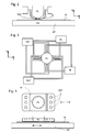
- FIG. 4 A further immersion lithography solution with a localized liquid supply system is shown in Figure 4 .
- Liquid is supplied by two groove inlets IN on either side of the projection system PL and is removed by a plurality of discrete outlets OUT arranged radially outwardly of the inlets IN.
- the inlets IN and OUT can be arranged in a plate with a hole in its center and through which the projection beam is projected.
- Liquid is supplied by one groove inlet IN on one side of the projection system PL and removed by a plurality of discrete outlets OUT on the other side of the projection system PL, causing a flow of a thin film of liquid between the projection system PL and the substrate W.
- the choice of which combination of inlet IN and outlets OUT to use can depend on the direction of movement of the substrate W (the other combination of inlet IN and outlets OUT being inactive).
- Immersion liquid may lift debris or particles (e.g. left over from the manufacturing process) from parts of the lithographic apparatus and/or substrates or erode components so as to introduce particles. This debris may then be left behind on the substrate after imaging or may interfere with the imaging while in suspension in the liquid between the projection system and the substrate. Thus, the issue of contamination should be addressed in an immersion lithographic apparatus.
- an immersion lithographic projection apparatus comprising: a substrate table constructed and arranged to hold a substrate; a projection system configured to project a patterned beam of radiation onto the substrate; a megasonic transducer configured to clean a surface; and a liquid supply system constructed and arranged to supply liquid between the megasonic transducer and the surface to be cleaned.
- an immersion lithographic projection apparatus comprising: a substrate table constructed and arranged to hold a substrate; a projection system configured to project a patterned beam of radiation onto the substrate; a megasonic transducer configured to clean a surface, the megasonic transducer being moveable relative to the surface such that, in a cleaning mode, a direct straight path through liquid exists between the megasonic transducer and the surface; and a liquid supply system configured to provide liquid between the transducer and the surface.
- a method of cleaning a surface of an immersion lithographic projection apparatus comprising: covering at least a part of the surface to be cleaned in liquid; and introducing megasonic waves into the liquid.
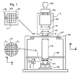
- Figure 1 depicts a lithographic apparatus according to an embodiment of the invention
- Figures 2 and 3 depict a liquid supply system for use in a lithographic projection apparatus
- Figure 4 depicts a another liquid supply system for use in a lithographic projection apparatus
- Figure 5 depicts, in cross-section, another liquid supply system for use in an immersion lithographic apparatus
- Figure 6 illustrates, in cross-section, a first embodiment of the present invention to clean a substrate table
- Figure 7 illustrates, in cross-section, a second embodiment of the present invention to clean a liquid supply system
- Figure 8 illustrates, in cross-section, a third embodiment of the invention to clean a substrate table.
- Figure 1 schematically depicts a lithographic apparatus according to one embodiment of the invention.
- the apparatus comprises:
- an illumination system (illuminator) IL configured to condition a radiation beam B (e.g. UV radiation or DUV radiation);
- a radiation beam B e.g. UV radiation or DUV radiation
- a support structure e.g. a mask table
- MT constructed to support a patterning device (e.g. a mask) MA and connected to a first positioner PM configured to accurately position the patterning device in accordance with certain parameters;
- a substrate table e.g. a wafer table
- WT constructed to hold a substrate (e.g. a resist-coated wafer) W and connected to a second positioner PW configured to accurately position the substrate in accordance with certain parameters
- a projection system e.g. a refractive projection lens system
- PS configured to project a pattern imparted to the radiation beam B by patterning device MA onto a target portion C (e.g. comprising one or more dies) of the substrate W.
- the illumination system may include various types of optical components, such as refractive, reflective, magnetic, electromagnetic, electrostatic or other types of optical components, or any combination thereof, for directing, shaping, or controlling radiation.
- optical components such as refractive, reflective, magnetic, electromagnetic, electrostatic or other types of optical components, or any combination thereof, for directing, shaping, or controlling radiation.
- the support structure holds the patterning device in a manner that depends on the orientation of the patterning device, the design of the lithographic apparatus, and other conditions, such as for example whether or not the patterning device is held in a vacuum environment.
- the support structure can use mechanical, vacuum, electrostatic or other clamping techniques to hold the patterning device.
- the support structure may be a frame or a table, for example, which may be fixed or movable as required.
- the support structure may ensure that the patterning device is at a desired position, for example with respect to the projection system. Any use of the terms "reticle” or “mask” herein may be considered synonymous with the more general term "patterning device.”
- patterning device used herein should be broadly interpreted as referring to any device that can be used to impart a radiation beam with a pattern in its cross-section such as to create a pattern in a target portion of the substrate. It should be noted that the pattern imparted to the radiation beam may not exactly correspond to the desired pattern in the target portion of the substrate, for example if the pattern includes phase-shifting features or so called assist features. Generally, the pattern imparted to the radiation beam will correspond to a particular functional layer in a device being created in the target portion, such as an integrated circuit.
- the patterning device may be transmissive or reflective.
- Examples of patterning devices include masks, programmable mirror arrays, and programmable LCD panels.
- Masks are well known in lithography, and include mask types such as binary, alternating phase-shift, and attenuated phase-shift, as well as various hybrid mask types.
- An example of a programmable mirror array employs a matrix arrangement of small mirrors, each of which can be individually tilted so as to reflect an incoming radiation beam in different directions. The tilted mirrors impart a pattern in a radiation beam which is reflected by the mirror matrix.
- projection system used herein should be broadly interpreted as encompassing any type of projection system, including refractive, reflective, catadioptric, magnetic, electromagnetic and electrostatic optical systems, or any combination thereof, as appropriate for the exposure radiation being used, or for other factors such as the use of an immersion liquid or the use of a vacuum. Any use of the term “projection lens” herein may be considered as synonymous with the more general term “projection system”.
- the apparatus is of a transmissive type (e.g. employing a transmissive mask).
- the apparatus may be of a reflective type (e.g. employing a programmable mirror array of a type as referred to above, or employing a reflective mask).
- the lithographic apparatus may be of a type having two (dual stage) or more substrate tables (and/or two or more support structures). In such "multiple stage” machines the additional tables may be used in parallel, or preparatory steps may be carried out on one or more tables while one or more other tables are being used for exposure.
- the illuminator IL receives a radiation beam from a radiation source SO.
- the source and the lithographic apparatus may be separate entities, for example when the source is an excimer laser. In such cases, the source is not considered to form part of the lithographic apparatus and the radiation beam is passed from the source SO to the illuminator IL with the aid of a beam delivery system BD comprising for example, suitable directing mirrors and/or a beam expander. In other cases the source may be an integral part of the lithographic apparatus, for example when the source is a mercury lamp.
- the source SO and the illuminator IL, together with the beam delivery system BD if required, may be referred to as a radiation system.
- the illuminator IL may comprise an adjuster AD for adjusting the angular intensity distribution of the radiation beam.
- an adjuster AD for adjusting the angular intensity distribution of the radiation beam.
- the illuminator IL may comprise various other components, such as an integrator IN and a condenser CO.
- the illuminator may be used to condition the radiation beam, to have a desired uniformity and intensity distribution in its cross-section.
- the radiation beam B is incident on the patterning device (e.g., mask) MA, which is held on the support structure (e.g., mask table) MT, and is patterned by the patterning device. Having traversed the patterning device MA, the radiation beam B passes through the projection system PS, which focuses the beam onto a target portion C of the substrate W.
- the substrate table WT can be moved accurately, e.g. so as to position different target portions C in the path of the radiation beam B.
- the first positioner PM and another position sensor can be used to accurately position the patterning device MA with respect to the path of the radiation beam B, e.g. after mechanical retrieval from a mask library, or during a scan.
- movement of the support structure MT may be realized with the aid of a long-stroke module (coarse positioning) and a short-stroke module (fine positioning), which form part of the first positioner PM.
- movement of the substrate table WT may be realized using a long-stroke module and a short-stroke module, which form part of the second positioner PW.
- the support structure MT may be connected to a short-stroke actuator only, or may be fixed.
- Patterning device MA and substrate W may be aligned using patterning device alignment marks M1, M2 and substrate alignment marks P1, P2.
- the substrate alignment marks as illustrated occupy dedicated target portions, they may be located in spaces between target portions (these are known as scribe-lane alignment marks).
- the patterning device alignment marks may be located between the dies.
- the depicted apparatus could be used in at least one of the following modes:
- step mode the support structure MT and the substrate table WT are kept essentially stationary, while an entire pattern imparted to the radiation beam is projected onto a target portion C at one time (i.e. a single static exposure).
- the substrate table WT is then shifted in the X and/or Y direction so that a different target portion C can be exposed.
- step mode the maximum size of the exposure field limits the size of the target portion C imaged in a single static exposure.
- the support structure MT and the substrate table WT are scanned synchronously while a pattern imparted to the radiation beam is projected onto a target portion C (i.e. a single dynamic exposure).
- the velocity and direction of the substrate table WT relative to the support structure MT may be determined by the (de-)magnification and image reversal characteristics of the projection system PS.
- the maximum size of the exposure field limits the width (in the non-scanning direction) of the target portion in a single dynamic exposure, whereas the length of the scanning motion determines the height (in the scanning direction) of the target portion.
- the support structure MT is kept essentially stationary holding a programmable patterning device, and the substrate table WT is moved or scanned while a pattern imparted to the radiation beam is projected onto a target portion C.
- a pulsed radiation source is employed and the programmable patterning device is updated as required after each movement of the substrate table WT or in between successive radiation pulses during a scan.
- This mode of operation can be readily applied to maskless lithography that utilizes programmable patterning device, such as a programmable mirror array of a type as referred to above.
- FIG. 5 Another immersion lithography solution with a localized liquid supply system solution which has been proposed is to provide the liquid supply system with a barrier member which extends along at least a part of a boundary of the space between the final element of the projection system and the substrate table.
- the barrier member is substantially stationary relative to the projection system in the XY plane though there may be some relative movement in the Z direction (in the direction of the optical axis).
- a seal is formed between the barrier member and the surface of the substrate and may be a contactless seal such as a gas seal.
- the barrier member 12 at least partly contains liquid in the space 11 between a final element of the projection system PS and the substrate W.
- a contactless seal 16 to the substrate may be formed around the image field of the projection system so that liquid is confined within the space between the substrate surface and the final element of the projection system.
- the space is at least partly formed by the barrier member 12 positioned below and surrounding the final element of the projection system PS. Liquid is brought into the space below the projection system and within the barrier member 12 by liquid inlet 13 and may be removed by liquid outlet 13.
- the barrier member 12 may extend a little above the final element of the projection system and the liquid level rises above the final element so that a buffer of liquid is provided.
- the barrier member 12 has an inner periphery that at the upper end, in an embodiment, closely conforms to the shape of the projection system or the final element thereof and may, e.g., be round.
- the liquid is contained in the space 11 by a gas seal 16 which, during use, is formed between the bottom of the barrier member 12 and the surface of the substrate W.
- the gas seal is formed by gas, e.g. air or synthetic air but, in an embodiment, N 2 or another inert gas, provided under pressure via inlet 15 to the gap between barrier member 12 and substrate and extracted via outlet 14.
- gas e.g. air or synthetic air but, in an embodiment, N 2 or another inert gas
- Those inlets/outlets may be annular grooves which surround the space 11 and the flow of gas 16 is effective to contain the liquid in the space 11.
- Such a system is disclosed in United States patent application publication no. US 2004-0207824 , hereby incorporated in its entirety by reference.
- an immersion lithographic apparatus is one in which a substrate is imaged through liquid. That is, an immersion liquid is provided between a final element of the projection system PS and the substrate.
- This arrangement may pose one or more particular problems.
- the liquid should be confined in the apparatus and also the liquid should be kept as free as possible of foreign object particles which may cause defects during imaging and/or by being left on the substrate surface after imaging and prior to downstream processing.
- the immersion liquid includes particles in suspension deliberately.
- One or more embodiments of the present invention addresses the problem of foreign object particles by providing an apparatus and a method to clean an immersion lithographic projection apparatus in which a cleaning liquid is applied to the surface to be cleaned and megasonic waves are introduced into the liquid to clean the surface.
- the cleaning liquid may or may not be the same as the immersion liquid. It could, for example, be ultra pure water.
- megasonic waves Compared to ultrasonic waves, megasonic waves produce cavitation bubbles (which implode or vibrate) which are very small and therefore may go very close to the surface to be cleaned.
- ultrasonic energy may be introduced into a liquid anywhere and will be distributed throughout the liquid
- megasonic energy is only locally high and must therefore be directed directly to the surface to be cleaned. That is, a direct path (line of sight/straight) must be present between the transducer introducing the megasonic waves and the surface to be cleaned. The whole length of that path should be filled with liquid.
- Megasonic frequencies are generally regarded to be between 750 kHz to 3 MHz. For the present purposes frequencies of above about 750 kHz, above 1 MHz or above 1.5 MHz are used.
- a stagnant boundary layer in the cleaning fluid near the surface of an object to be cleaned becomes thinner as frequency of the introduced sonic energy is increased.
- cleaning is partly accomplished by acoustic streaming with high velocity pressure waves in the cleaning fluid as well as bubble vibration and, to a lesser extent cavitation and bubble bursting.
- gas may be dissolved into the liquid to promote cavitation (bubble formation). Suitable gases are nitrogen, carbon dioxide or oxygen but other gases may also be suitable such as ozone, or hydrogen (containing water).
- a surfactant in the liquid can further enhance cleaning efficiency.
- Other possibilities to enhance cleaning efficiency include using a detergent or a solvent in the cleaning liquid or adding H 2 O 2 solution.
- Objects which one might want to clean in an immersion lithographic apparatus include, but not limited to, the substrate table WT which supports the substrate W (its top surface), the final element of the projection system PS which is immersed in immersion liquid during imaging and parts of the liquid confinement system (for example those illustrated in Figures 2-5 ) which provides liquid between the final element of the projection system PS and the substrate W during imaging.
- a liquid supply system is provided to provide liquid between a megasonic transducer and the surface to be cleaned.
- the liquid supply system provides a flow of liquid so that liquid is removed as the surface is cleaned such that particles removed from the surface are carried away.
- One suitable liquid is water in an ultra pure form.
- other types of liquid may be suitable.
- an addition to the liquid such as a surfactant as mentioned above may also have an advantage.
- Other cleaning liquids are water/hydrogen peroxide, water/ethanol, water/iso-propylalcohol (IPA), water/ammonia or water/acetone mixtures, for example.
- Other chemicals which may be useful as an addition include TMAH and SC-1 or SC-2.
- a process time up to 100 seconds may lead to a particle removal efficiency of up to 100% at a frequency of about 1 MHz. If the acoustic frequency exceeds much more than 3 MHz the particle removal efficiency is dramatically decreased over a frequency of just above 1 MHz.
- the introduction of gas into the liquid has a major effect on the particle removal efficiency. Removal of 34 nm diameter SiO 2 particles may increase from zero removal efficiency to 30% removal efficiency with the introduction of oxygen at a level of 20 ppm into the liquid. Thus, a gas concentration of above about 5 ppm can be useful.
- Temperature may also be important and a balance should be drawn between faster reaction time at a high temperature (say 55°C) over less gas being dissolved at a high temperature.
- the power of the transducer should be between 0.2 and 5 W/cm 2 , the irradiation distance should be between 5 and 20 mm and a cleaning time should be between 10 and 90 seconds.
- acoustic waves from the megasonic transducer to travel a direct path to the surface to be cleaned from the megasonic transducer, several designs are proposed to clean different parts of the immersion lithographic apparatus.
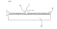
- a first embodiment is illustrated in Figure 6 which may be used, for instance, to clean a top surface of a substrate table WT.
- the liquid supply system comprises a barrier member 12 which surrounds a transducer 20.
- the barrier member 12 could be similar to that of the liquid confinement system of Figure 5 in that it comprises a gas seal device 14, 15 to create a seal between the bottom of the barrier member 12 and the top surface of the substrate table WT using a flow of gas 16.
- the transducer 20 which fits inside the barrier member 12 may thereby be positioned very close to the surface of the substrate table WT. This is an advantage because the transducer 20 should be quite small in order to fit inside the barrier member 12 and therefore should be positioned relatively close to the top surface of the substrate table WT being cleaned (because it has low power).
- the megasonic transducer 20 is less than 1.5 mm or less than 1.6 mm away from the surface it is cleaning.
- a flow of liquid is provided across the barrier member 12 and the bottom of the transducer 20 is covered in liquid.
- the substrate table WT and/or the barrier member 12 and transducer 20 are moved relative to the other so that all of the top surface of the substrate table WT may be cleaned.
- the cleaning could take place within the lithographic apparatus in an automated way or could be carried out manually bypassing the barrier member 12 and transducer 20 over the top surface of the substrate table WT by hand or by some tooling.
- the cleaning process is automated, one way of arranging for this is to provide the barrier member 12 and transducer 20 arrangement to be moveable from a stationary store position to a (stationary) clean position and to move the substrate table WT relative to the transducer 20 when the transducer is in the (stationary) clean position.
- the substrate table WT may need to be moved in the Z axis prior to activation of the liquid supply system of the cleaning device.
- Figure 7 illustrates a second embodiment which is used in order to clean a liquid confinement system LCS, such as one illustrated in Figures 2-5 , which is positioned around the final element of the projection system PS.
- a liquid confinement system in accordance with that shown in Figure 5 is illustrated as an example.
- a moveable bath 50 which has on its bottom surface a megasonic transducer 20.
- the megasonic transducer 20 of the second embodiment may be larger than the megasonic transducer of the first embodiment because there are no particular size constraints.
- the distance between the megasonic transducer and the surface to be cleaned can be made larger and up to 50 mm. In an embodiment, the distance is less than 40 mm or less than 30 mm.
- a controller controls the position of the bath 50 which is moveable between a store position and a cleaning position (as illustrated) and which controls the level of fluid in the bath 50.
- the level of liquid is controlled so as to cover the bottom surface of the liquid confinement system LCS but not to cover the final element of the projection system PS.
- the gap 75 is not filled with liquid. This is to protect the final element of the projection system from the sonic waves and/or the cleaning liquid which could damage it.
- a shield (perhaps in the form of a plate) may be used to shield the final element of the projection system from megasonic waves and/or liquid.
- this bath arrangement may be used to clean the final element of the projection system PS and in which case the controller increases the level of liquid in the bath 50 so that the final element of the projection system PS is covered in liquid.
- the bath 50 and/or transducer 20 may be moveable relative to the projection system PS in the cleaning position and liquid confinement system LCS such that the whole under surface of the liquid confinement system LCS may be cleaned.
- the substrate table WT is provided with a retractable barrier 80 which, in its clean position extends above and around the top surface of the substrate table WT to be cleaned.
- a megasonic transducer 20 can be moved over the surface of the substrate table WT (with the bottom surface of the transducer 20 covered by liquid) and/or the substrate table WT may be moved under the transducer 20, thereby to clean the top surface of the substrate table WT.
- the barrier 80 is not retractable and is permanently attached to the substrate table WT or is a removable part.
- the transducer 20 could be fixed or moveable (particularly in the Z direction) and/or also moveable in the X/Y axis during the cleaning operation.
- sensors When the top surface of the substrate table WT is cleaned, it is also possible to clean at the same time one or more sensors provided on the top surface of the substrate table WT.
- types of sensors include a transmission image sensor, a lens interferometer, and/or a spot sensor.
- a micrometer may be provided to adjust the tilt of the transducer 20 relative to the surface to be cleaned.
- a micrometer may also be used to adjust the distance from the transducer to the surface to be cleaned. In all embodiments, a flow of liquid across the distance between the transducer and the surface to be cleaned is desirable though not essential.
- the above described megasonic cleaner is well suited to removing particles from a surface. However, once those particles have been removed they sometimes re-attach themselves to a surface unless the liquid in which the particles are suspended is quickly moved away. Therefore, it is desirable to provide a flow of liquid between the megasonic transducer and the surface being cleaned. In particular, it is desirable to design the apparatus such that there are no locations of zero flow velocity (stagnant zones).
- Another way to prevent or at least reduce re-attachment of the particles to the surface is to change the properties of the liquid between the transducer and the surface to ensure that the zeta potential of the particles and the zeta potential of the surface is such that the particles are not attracted to the surface, preferably such that they are repelled from the surface.
- the zeta potential is the potential of a surface in a liquid.
- the zeta potential generally decreases with distance from the surface.
- a given type of material has a given zeta potential for a particular type of liquid.
- One way of varying the zeta potential of a surface is to change the concentration of electrolyte in the liquid and another method to change the zeta potential is to change the pH of the liquid.
- concentration of electrolyte in the liquid (e.g. salt) or the pH of the liquid (i) the zeta potential of the surface from which the particles are removed (and/or any other surface where adherence is to be avoided) and (ii) the zeta potential of the particles can be chosen.
- those two zeta potentials are chosen such that they have the same polarity and thereby repel.
- the pH of the liquid and/or concentration of the electrolyte chosen with a knowledge of the material from which the surface which is being cleaned is made and with a knowledge of the type of material the particles are likely to be made. If the materials are the same, then it should easy to select a pH or electrolyte concentration at which the zeta potential is non zero for both the surface and the particle. In that circumstance the potential would be either positive or negative for both the surface and the particle such that they would repel one another and the particles would be unlikely to re-adhere to the surface. If the materials are different, pH or electrolyte concentration may be harder to choose, but it is likely that there will be at least one pH and/or concentration at which the zeta potential will have the same polarity for both materials.
- lithographic apparatus in the manufacture of ICs
- the lithographic apparatus described herein may have other applications, such as the manufacture of integrated optical systems, guidance and detection patterns for magnetic domain memories, flat-panel displays, liquid-crystal displays (LCDs), thin-film magnetic heads, etc.
- LCDs liquid-crystal displays
- any use of the terms “wafer” or “die” herein may be considered as synonymous with the more general terms “substrate” or "target portion”, respectively.
- the substrate referred to herein may be processed, before or after exposure, in for example a track (a tool that typically applies a layer of resist to a substrate and develops the exposed resist), a metrology tool and/or an inspection tool. Where applicable, the disclosure herein may be applied to such and other substrate processing tools. Further, the substrate may be processed more than once, for example in order to create a multi-layer IC, so that the term substrate used herein may also refer to a substrate that already contains multiple processed layers.
- UV radiation e.g. having a wavelength of or about 365, 248, 193, 157 or 126 nm.
- lens may refer to any one or combination of various types of optical components, including refractive and reflective optical components.
- the invention may take the form of a computer program containing one or more sequences of machine-readable instructions describing a method as disclosed above, or a data storage medium (e.g. semiconductor memory, magnetic or optical disk) having such a computer program stored therein.
- a data storage medium e.g. semiconductor memory, magnetic or optical disk
- a liquid supply system as contemplated herein should be broadly construed. In certain embodiments, it may be a mechanism or combination of structures that provides a liquid to a space between the projection system and the substrate and/or substrate table. It may comprise a combination of one or more structures, one or more liquid inlets, one or more gas inlets, one or more gas outlets, and/or one or more liquid outlets that provide liquid to the space.
- a surface of the space may be a portion of the substrate and/or substrate table, or a surface of the space may completely cover a surface of the substrate and/or substrate table, or the space may envelop the substrate and/or substrate table.
- the liquid supply system may optionally further include one or more elements to control the position, quantity, quality, shape, flow rate or any other features of the liquid.
- the immersion liquid used in the apparatus may have different compositions, according to the desired properties and the wavelength of exposure radiation used. For an exposure wavelength of 193nm, ultra pure water or water-based compositions may be used and for this reason the immersion liquid is sometimes referred to as water and water-related terms such as hydrophilic, hydrophobic, humidity, etc. may be used.
Applications Claiming Priority (2)
| Application Number | Priority Date | Filing Date | Title |
|---|---|---|---|
| US11/437,876 US7969548B2 (en) | 2006-05-22 | 2006-05-22 | Lithographic apparatus and lithographic apparatus cleaning method |
| EP07251915A EP1860507B1 (de) | 2006-05-22 | 2007-05-09 | Lithographievorrichtung und Reinigungsverfahren dafür |
Related Parent Applications (2)
| Application Number | Title | Priority Date | Filing Date |
|---|---|---|---|
| EP07251915.0 Division | 2007-05-09 | ||
| EP07251915 Previously-Filed-Application | 2007-05-09 |
Publications (2)
| Publication Number | Publication Date |
|---|---|
| EP2365391A2 true EP2365391A2 (de) | 2011-09-14 |
| EP2365391A3 EP2365391A3 (de) | 2012-08-29 |
Family
ID=38181126
Family Applications (2)
| Application Number | Title | Priority Date | Filing Date |
|---|---|---|---|
| EP07251915A Not-in-force EP1860507B1 (de) | 2006-05-22 | 2007-05-09 | Lithographievorrichtung und Reinigungsverfahren dafür |
| EP11164878A Withdrawn EP2365391A3 (de) | 2006-05-22 | 2007-05-09 | Lithographievorrichtung und Reinigungsverfahren dafür |
Family Applications Before (1)
| Application Number | Title | Priority Date | Filing Date |
|---|---|---|---|
| EP07251915A Not-in-force EP1860507B1 (de) | 2006-05-22 | 2007-05-09 | Lithographievorrichtung und Reinigungsverfahren dafür |
Country Status (7)
| Country | Link |
|---|---|
| US (3) | US7969548B2 (de) |
| EP (2) | EP1860507B1 (de) |
| JP (3) | JP4691066B2 (de) |
| KR (3) | KR100897862B1 (de) |
| CN (2) | CN102081310A (de) |
| SG (1) | SG137811A1 (de) |
| TW (2) | TWI367401B (de) |
Families Citing this family (47)
| Publication number | Priority date | Publication date | Assignee | Title |
|---|---|---|---|---|
| US7684008B2 (en) | 2003-06-11 | 2010-03-23 | Asml Netherlands B.V. | Lithographic apparatus and device manufacturing method |
| US7050146B2 (en) | 2004-02-09 | 2006-05-23 | Asml Netherlands B.V. | Lithographic apparatus and device manufacturing method |
| US7385670B2 (en) * | 2004-10-05 | 2008-06-10 | Asml Netherlands B.V. | Lithographic apparatus, cleaning system and cleaning method for in situ removing contamination from a component in a lithographic apparatus |
| EP1821337B1 (de) * | 2004-12-06 | 2016-05-11 | Nikon Corporation | Wartungsverfahren |
| US7880860B2 (en) | 2004-12-20 | 2011-02-01 | Asml Netherlands B.V. | Lithographic apparatus and device manufacturing method |
| CN100565799C (zh) * | 2005-07-11 | 2009-12-02 | 株式会社尼康 | 曝光装置及元件制造方法 |
| US8125610B2 (en) | 2005-12-02 | 2012-02-28 | ASML Metherlands B.V. | Method for preventing or reducing contamination of an immersion type projection apparatus and an immersion type lithographic apparatus |
| CN101410948B (zh) * | 2006-05-18 | 2011-10-26 | 株式会社尼康 | 曝光方法及装置、维护方法、以及组件制造方法 |
| US7969548B2 (en) * | 2006-05-22 | 2011-06-28 | Asml Netherlands B.V. | Lithographic apparatus and lithographic apparatus cleaning method |
| TW200818256A (en) * | 2006-05-22 | 2008-04-16 | Nikon Corp | Exposure method and apparatus, maintenance method, and device manufacturing method |
| CN101385124B (zh) * | 2006-05-23 | 2011-02-09 | 株式会社尼康 | 维修方法、曝光方法及装置、以及组件制造方法 |
| EP2043134A4 (de) * | 2006-06-30 | 2012-01-25 | Nikon Corp | Wartungsverfahren, belichtungsverfahren und vorrichtung und bauelementeherstellungsverfahren |
| WO2008029884A1 (fr) * | 2006-09-08 | 2008-03-13 | Nikon Corporation | Dispositif et procédé de nettoyage, et procédé de fabrication du dispositif |
| US20080156356A1 (en) * | 2006-12-05 | 2008-07-03 | Nikon Corporation | Cleaning liquid, cleaning method, liquid generating apparatus, exposure apparatus, and device fabricating method |
| US8654305B2 (en) | 2007-02-15 | 2014-02-18 | Asml Holding N.V. | Systems and methods for insitu lens cleaning in immersion lithography |
| US8817226B2 (en) | 2007-02-15 | 2014-08-26 | Asml Holding N.V. | Systems and methods for insitu lens cleaning using ozone in immersion lithography |
| JP2010519722A (ja) * | 2007-02-23 | 2010-06-03 | 株式会社ニコン | 露光方法、露光装置、デバイス製造方法、及び液浸露光用基板 |
| US9013672B2 (en) * | 2007-05-04 | 2015-04-21 | Asml Netherlands B.V. | Cleaning device, a lithographic apparatus and a lithographic apparatus cleaning method |
| US7866330B2 (en) * | 2007-05-04 | 2011-01-11 | Asml Netherlands B.V. | Cleaning device, a lithographic apparatus and a lithographic apparatus cleaning method |
| US8011377B2 (en) * | 2007-05-04 | 2011-09-06 | Asml Netherlands B.V. | Cleaning device and a lithographic apparatus cleaning method |
| US8947629B2 (en) | 2007-05-04 | 2015-02-03 | Asml Netherlands B.V. | Cleaning device, a lithographic apparatus and a lithographic apparatus cleaning method |
| US8098362B2 (en) * | 2007-05-30 | 2012-01-17 | Nikon Corporation | Detection device, movable body apparatus, pattern formation apparatus and pattern formation method, exposure apparatus and exposure method, and device manufacturing method |
| US7916269B2 (en) | 2007-07-24 | 2011-03-29 | Asml Netherlands B.V. | Lithographic apparatus and contamination removal or prevention method |
| US9019466B2 (en) | 2007-07-24 | 2015-04-28 | Asml Netherlands B.V. | Lithographic apparatus, reflective member and a method of irradiating the underside of a liquid supply system |
| NL1035942A1 (nl) * | 2007-09-27 | 2009-03-30 | Asml Netherlands Bv | Lithographic Apparatus and Method of Cleaning a Lithographic Apparatus. |
| SG151198A1 (en) * | 2007-09-27 | 2009-04-30 | Asml Netherlands Bv | Methods relating to immersion lithography and an immersion lithographic apparatus |
| JP5017232B2 (ja) * | 2007-10-31 | 2012-09-05 | エーエスエムエル ネザーランズ ビー.ブイ. | クリーニング装置および液浸リソグラフィ装置 |
| NL1036273A1 (nl) * | 2007-12-18 | 2009-06-19 | Asml Netherlands Bv | Lithographic apparatus and method of cleaning a surface of an immersion lithographic apparatus. |
| NL1036306A1 (nl) | 2007-12-20 | 2009-06-23 | Asml Netherlands Bv | Lithographic apparatus and in-line cleaning apparatus. |
| KR101423611B1 (ko) * | 2008-01-16 | 2014-07-30 | 삼성전자주식회사 | 기판 처리 장치, 노광 장치 및 클리닝 툴의 세정 방법 |
| US8339572B2 (en) | 2008-01-25 | 2012-12-25 | Asml Netherlands B.V. | Lithographic apparatus and device manufacturing method |
| NL1036571A1 (nl) * | 2008-03-07 | 2009-09-08 | Asml Netherlands Bv | Lithographic Apparatus and Methods. |
| KR101160948B1 (ko) | 2008-04-16 | 2012-06-28 | 에이에스엠엘 네델란즈 비.브이. | 리소그래피 장치 |
| US8619231B2 (en) * | 2009-05-21 | 2013-12-31 | Nikon Corporation | Cleaning method, exposure method, and device manufacturing method |
| NL2005610A (en) | 2009-12-02 | 2011-06-06 | Asml Netherlands Bv | Lithographic apparatus and surface cleaning method. |
| MX2012007581A (es) * | 2009-12-28 | 2012-07-30 | Pioneer Hi Bred Int | Genotipos restauradores de la fertilidad de sorgo y metodos de seleccion asistida por marcadores. |
| US20120160264A1 (en) * | 2010-12-23 | 2012-06-28 | Richard Endo | Wet Processing Tool with Site Isolation |
| US8974606B2 (en) | 2011-05-09 | 2015-03-10 | Intermolecular, Inc. | Ex-situ cleaning assembly |
| JP5893882B2 (ja) * | 2011-09-28 | 2016-03-23 | 東京エレクトロン株式会社 | パーティクル捕集装置及びパーティクルの捕集方法 |
| US9005366B2 (en) | 2011-10-06 | 2015-04-14 | Intermolecular, Inc. | In-situ reactor cleaning in high productivity combinatorial system |
| CN102629567B (zh) * | 2011-10-19 | 2015-06-24 | 京东方科技集团股份有限公司 | 一种基板固定装置及制作方法以及固定基板的方法 |
| TWI576657B (zh) * | 2014-12-25 | 2017-04-01 | 台灣積體電路製造股份有限公司 | 光罩清潔設備以及光罩清潔方法 |
| JP5963929B1 (ja) * | 2015-09-04 | 2016-08-03 | 株式会社日立パワーソリューションズ | 超音波検査装置、超音波検査システム、及び超音波検査方法 |
| US10256132B2 (en) * | 2016-04-28 | 2019-04-09 | Varian Semiconductor Equipment Associates, Inc. | Reticle processing system |
| CN107619098A (zh) * | 2016-08-19 | 2018-01-23 | Mag技术株式会社 | 碳酸氢气水及其在基板表面的应用 |
| CN109994372A (zh) * | 2019-04-15 | 2019-07-09 | 西安奕斯伟硅片技术有限公司 | 晶圆清洗方法及晶圆清洗装置 |
| CN110711739A (zh) * | 2019-09-29 | 2020-01-21 | 中国科学院长春光学精密机械与物理研究所 | 一种用于深紫外CaF2光学基底的清洗方法 |
Citations (6)
| Publication number | Priority date | Publication date | Assignee | Title |
|---|---|---|---|---|
| US5783790A (en) * | 1995-11-30 | 1998-07-21 | Organo Corporation | Wet treatment method |
| EP1429189A1 (de) * | 2002-12-13 | 2004-06-16 | ASML Netherlands B.V. | Lithographischer Apparat und Verfahren zur Herstellung einer Vorrichtung |
| EP1486827A2 (de) * | 2003-06-11 | 2004-12-15 | ASML Netherlands B.V. | Lithographischer Apparat und Verfahren zur Herstellung einer Vorrichtung |
| US20060028628A1 (en) * | 2004-08-03 | 2006-02-09 | Taiwan Semiconductor Manufacturing Co., Ltd. | Lens cleaning module |
| US20060103818A1 (en) * | 2004-11-18 | 2006-05-18 | International Business Machines Corporation | Method and apparatus for cleaning a semiconductor substrate in an immersion lithography system |
| EP1777589A2 (de) * | 2005-10-24 | 2007-04-25 | Taiwan Semiconductor Manufacturing Co., Ltd. | Vorrichtung und Verfahren zur Immersionslithographie |
Family Cites Families (163)
| Publication number | Priority date | Publication date | Assignee | Title |
|---|---|---|---|---|
| GB1242527A (en) | 1967-10-20 | 1971-08-11 | Kodak Ltd | Optical instruments |
| US3573975A (en) | 1968-07-10 | 1971-04-06 | Ibm | Photochemical fabrication process |
| EP0023231B1 (de) | 1979-07-27 | 1982-08-11 | Tabarelli, Werner, Dr. | Optisches Lithographieverfahren und Einrichtung zum Kopieren eines Musters auf eine Halbleiterscheibe |
| FR2474708B1 (fr) | 1980-01-24 | 1987-02-20 | Dme | Procede de microphotolithographie a haute resolution de traits |
| JPS5754317A (en) | 1980-09-19 | 1982-03-31 | Hitachi Ltd | Method and device for forming pattern |
| US4346164A (en) | 1980-10-06 | 1982-08-24 | Werner Tabarelli | Photolithographic method for the manufacture of integrated circuits |
| US4509852A (en) | 1980-10-06 | 1985-04-09 | Werner Tabarelli | Apparatus for the photolithographic manufacture of integrated circuit elements |
| US4390273A (en) | 1981-02-17 | 1983-06-28 | Censor Patent-Und Versuchsanstalt | Projection mask as well as a method and apparatus for the embedding thereof and projection printing system |
| JPS57153433A (en) | 1981-03-18 | 1982-09-22 | Hitachi Ltd | Manufacturing device for semiconductor |
| US4405701A (en) | 1981-07-29 | 1983-09-20 | Western Electric Co. | Methods of fabricating a photomask |
| US5040020A (en) | 1988-03-31 | 1991-08-13 | Cornell Research Foundation, Inc. | Self-aligned, high resolution resonant dielectric lithography |
| JPH03209479A (ja) | 1989-09-06 | 1991-09-12 | Sanee Giken Kk | 露光方法 |
| US5143103A (en) * | 1991-01-04 | 1992-09-01 | International Business Machines Corporation | Apparatus for cleaning and drying workpieces |
| US5121256A (en) | 1991-03-14 | 1992-06-09 | The Board Of Trustees Of The Leland Stanford Junior University | Lithography system employing a solid immersion lens |
| JP2753930B2 (ja) | 1992-11-27 | 1998-05-20 | キヤノン株式会社 | 液浸式投影露光装置 |
| JPH08316124A (ja) | 1995-05-19 | 1996-11-29 | Hitachi Ltd | 投影露光方法及び露光装置 |
| US6629640B2 (en) * | 1995-12-18 | 2003-10-07 | Metrologic Instruments, Inc. | Holographic laser scanning method and system employing visible scanning-zone indicators identifying a three-dimensional omni-directional laser scanning volume for package transport navigation |
| KR980012021A (ko) * | 1996-07-29 | 1998-04-30 | 김광호 | 반도체 소자의 세정방법 |
| US6104687A (en) | 1996-08-26 | 2000-08-15 | Digital Papyrus Corporation | Method and apparatus for coupling an optical lens to a disk through a coupling medium having a relatively high index of refraction |
| US5825043A (en) | 1996-10-07 | 1998-10-20 | Nikon Precision Inc. | Focusing and tilting adjustment system for lithography aligner, manufacturing apparatus or inspection apparatus |
| JPH1133506A (ja) * | 1997-07-24 | 1999-02-09 | Tadahiro Omi | 流体処理装置及び洗浄処理システム |
| US5900354A (en) | 1997-07-03 | 1999-05-04 | Batchelder; John Samuel | Method for optical inspection and lithography |
| JPH11162831A (ja) * | 1997-11-21 | 1999-06-18 | Nikon Corp | 投影露光装置及び投影露光方法 |
| WO1999027568A1 (fr) | 1997-11-21 | 1999-06-03 | Nikon Corporation | Graveur de motifs a projection et procede de sensibilisation a projection |
| JPH11176727A (ja) * | 1997-12-11 | 1999-07-02 | Nikon Corp | 投影露光装置 |
| US5837662A (en) | 1997-12-12 | 1998-11-17 | Memc Electronic Materials, Inc. | Post-lapping cleaning process for silicon wafers |
| WO1999031717A1 (fr) | 1997-12-12 | 1999-06-24 | Nikon Corporation | Procede d'exposition par projection et graveur a projection |
| JP2000058436A (ja) | 1998-08-11 | 2000-02-25 | Nikon Corp | 投影露光装置及び露光方法 |
| TWI242111B (en) | 1999-04-19 | 2005-10-21 | Asml Netherlands Bv | Gas bearings for use in vacuum chambers and their application in lithographic projection apparatus |
| JP2000323396A (ja) | 1999-05-13 | 2000-11-24 | Canon Inc | 露光方法、露光装置、およびデイバイス製造方法 |
| JP4504479B2 (ja) | 1999-09-21 | 2010-07-14 | オリンパス株式会社 | 顕微鏡用液浸対物レンズ |
| US6743301B2 (en) | 1999-12-24 | 2004-06-01 | mFSI Ltd. | Substrate treatment process and apparatus |
| US6523210B1 (en) * | 2000-04-05 | 2003-02-25 | Nicholas Andros | Surface charge controlling apparatus for wafer cleaning |
| US6539952B2 (en) * | 2000-04-25 | 2003-04-01 | Solid State Equipment Corp. | Megasonic treatment apparatus |
| US6927176B2 (en) * | 2000-06-26 | 2005-08-09 | Applied Materials, Inc. | Cleaning method and solution for cleaning a wafer in a single wafer process |
| TW591653B (en) | 2000-08-08 | 2004-06-11 | Koninkl Philips Electronics Nv | Method of manufacturing an optically scannable information carrier |
| JP2002075947A (ja) * | 2000-08-30 | 2002-03-15 | Alps Electric Co Ltd | ウェット処理装置 |
| US20020163629A1 (en) | 2001-05-07 | 2002-11-07 | Michael Switkes | Methods and apparatus employing an index matching medium |
| US6600547B2 (en) | 2001-09-24 | 2003-07-29 | Nikon Corporation | Sliding seal |
| CN1791839A (zh) | 2001-11-07 | 2006-06-21 | 应用材料有限公司 | 光点格栅阵列光刻机 |
| US6955485B2 (en) | 2002-03-01 | 2005-10-18 | Tokyo Electron Limited | Developing method and developing unit |
| DE10229818A1 (de) | 2002-06-28 | 2004-01-15 | Carl Zeiss Smt Ag | Verfahren zur Fokusdetektion und Abbildungssystem mit Fokusdetektionssystem |
| US7240679B2 (en) * | 2002-09-30 | 2007-07-10 | Lam Research Corporation | System for substrate processing with meniscus, vacuum, IPA vapor, drying manifold |
| US8236382B2 (en) | 2002-09-30 | 2012-08-07 | Lam Research Corporation | Proximity substrate preparation sequence, and method, apparatus, and system for implementing the same |
| US6788477B2 (en) | 2002-10-22 | 2004-09-07 | Taiwan Semiconductor Manufacturing Co., Ltd. | Apparatus for method for immersion lithography |
| EP1420300B1 (de) | 2002-11-12 | 2015-07-29 | ASML Netherlands B.V. | Lithographischer Apparat und Verfahren zur Herstellung einer Vorrichtung |
| DE60335595D1 (de) | 2002-11-12 | 2011-02-17 | Asml Netherlands Bv | Lithographischer Apparat mit Immersion und Verfahren zur Herstellung einer Vorrichtung |
| CN101382738B (zh) | 2002-11-12 | 2011-01-12 | Asml荷兰有限公司 | 光刻投射装置 |
| CN100470367C (zh) | 2002-11-12 | 2009-03-18 | Asml荷兰有限公司 | 光刻装置和器件制造方法 |
| KR100588124B1 (ko) | 2002-11-12 | 2006-06-09 | 에이에스엠엘 네델란즈 비.브이. | 리소그래피장치 및 디바이스제조방법 |
| SG121822A1 (en) | 2002-11-12 | 2006-05-26 | Asml Netherlands Bv | Lithographic apparatus and device manufacturing method |
| SG131766A1 (en) | 2002-11-18 | 2007-05-28 | Asml Netherlands Bv | Lithographic apparatus and device manufacturing method |
| WO2004050266A1 (ja) | 2002-12-03 | 2004-06-17 | Nikon Corporation | 汚染物質除去方法及び装置、並びに露光方法及び装置 |
| EP1571701A4 (de) | 2002-12-10 | 2008-04-09 | Nikon Corp | Belichtungsvorrichtungund verfahren zur bauelementeherstellung |
| AU2003289272A1 (en) | 2002-12-10 | 2004-06-30 | Nikon Corporation | Surface position detection apparatus, exposure method, and device porducing method |
| SG2011031200A (en) | 2002-12-10 | 2014-09-26 | Nippon Kogaku Kk | Exposure apparatus and device manufacturing method |
| WO2004053952A1 (ja) | 2002-12-10 | 2004-06-24 | Nikon Corporation | 露光装置及びデバイス製造方法 |
| AU2003302831A1 (en) | 2002-12-10 | 2004-06-30 | Nikon Corporation | Exposure method, exposure apparatus and method for manufacturing device |
| JP4232449B2 (ja) | 2002-12-10 | 2009-03-04 | 株式会社ニコン | 露光方法、露光装置、及びデバイス製造方法 |
| EP1571698A4 (de) | 2002-12-10 | 2006-06-21 | Nikon Corp | Belichtungsvorrichtung, belichtungsverfahren und verfahren zur herstellung von bauelementen |
| EP1571696A4 (de) | 2002-12-10 | 2008-03-26 | Nikon Corp | Expositionsgerüt und herstellungsverfahren dafür |
| EP1429190B1 (de) | 2002-12-10 | 2012-05-09 | Canon Kabushiki Kaisha | Belichtungsapparat und -verfahren |
| US7242455B2 (en) | 2002-12-10 | 2007-07-10 | Nikon Corporation | Exposure apparatus and method for producing device |
| AU2003289007A1 (en) | 2002-12-10 | 2004-06-30 | Nikon Corporation | Optical device and projection exposure apparatus using such optical device |
| JP4352874B2 (ja) | 2002-12-10 | 2009-10-28 | 株式会社ニコン | 露光装置及びデバイス製造方法 |
| DE10257766A1 (de) | 2002-12-10 | 2004-07-15 | Carl Zeiss Smt Ag | Verfahren zur Einstellung einer gewünschten optischen Eigenschaft eines Projektionsobjektivs sowie mikrolithografische Projektionsbelichtungsanlage |
| SG150388A1 (en) | 2002-12-10 | 2009-03-30 | Nikon Corp | Exposure apparatus and method for producing device |
| ATE424026T1 (de) | 2002-12-13 | 2009-03-15 | Koninkl Philips Electronics Nv | Flüssigkeitsentfernung in einem verfahren und einer einrichtung zum bestrahlen von flecken auf einer schicht |
| EP1584089B1 (de) | 2002-12-19 | 2006-08-02 | Koninklijke Philips Electronics N.V. | Verfahren und anordnung zum bestrahlen einer schicht mittels eines lichtpunkts |
| DE60314668T2 (de) | 2002-12-19 | 2008-03-06 | Koninklijke Philips Electronics N.V. | Verfahren und anordnung zum bestrahlen einer schicht mittels eines lichtpunkts |
| US6781670B2 (en) | 2002-12-30 | 2004-08-24 | Intel Corporation | Immersion lithography |
| JP4837556B2 (ja) | 2003-04-11 | 2011-12-14 | 株式会社ニコン | 液浸リソグラフィにおける光学素子の洗浄方法 |
| TWI295414B (en) | 2003-05-13 | 2008-04-01 | Asml Netherlands Bv | Lithographic apparatus and device manufacturing method |
| TW201806001A (zh) | 2003-05-23 | 2018-02-16 | 尼康股份有限公司 | 曝光裝置及元件製造方法 |
| US7274472B2 (en) | 2003-05-28 | 2007-09-25 | Timbre Technologies, Inc. | Resolution enhanced optical metrology |
| DE10324477A1 (de) * | 2003-05-30 | 2004-12-30 | Carl Zeiss Smt Ag | Mikrolithographische Projektionsbelichtungsanlage |
| JP4643582B2 (ja) * | 2003-06-11 | 2011-03-02 | アクリオン テクノロジーズ インク | 過飽和の洗浄溶液を使用したメガソニック洗浄 |
| JP2005019616A (ja) | 2003-06-25 | 2005-01-20 | Canon Inc | 液浸式露光装置 |
| JP4343597B2 (ja) | 2003-06-25 | 2009-10-14 | キヤノン株式会社 | 露光装置及びデバイス製造方法 |
| JP3862678B2 (ja) | 2003-06-27 | 2006-12-27 | キヤノン株式会社 | 露光装置及びデバイス製造方法 |
| EP1498778A1 (de) | 2003-06-27 | 2005-01-19 | ASML Netherlands B.V. | Lithographischer Apparat und Verfahren zur Herstellung einer Vorrichtung |
| US7738074B2 (en) | 2003-07-16 | 2010-06-15 | Asml Netherlands B.V. | Lithographic apparatus and device manufacturing method |
| US7370659B2 (en) * | 2003-08-06 | 2008-05-13 | Micron Technology, Inc. | Photolithographic stepper and/or scanner machines including cleaning devices and methods of cleaning photolithographic stepper and/or scanner machines |
| JP2005072404A (ja) | 2003-08-27 | 2005-03-17 | Sony Corp | 露光装置および半導体装置の製造方法 |
| JP4305095B2 (ja) | 2003-08-29 | 2009-07-29 | 株式会社ニコン | 光学部品の洗浄機構を搭載した液浸投影露光装置及び液浸光学部品洗浄方法 |
| US6954256B2 (en) | 2003-08-29 | 2005-10-11 | Asml Netherlands B.V. | Gradient immersion lithography |
| US7070915B2 (en) | 2003-08-29 | 2006-07-04 | Tokyo Electron Limited | Method and system for drying a substrate |
| US7014966B2 (en) | 2003-09-02 | 2006-03-21 | Advanced Micro Devices, Inc. | Method and apparatus for elimination of bubbles in immersion medium in immersion lithography systems |
| JP4378136B2 (ja) | 2003-09-04 | 2009-12-02 | キヤノン株式会社 | 露光装置及びデバイス製造方法 |
| JP3870182B2 (ja) | 2003-09-09 | 2007-01-17 | キヤノン株式会社 | 露光装置及びデバイス製造方法 |
| EP3007207B1 (de) | 2003-09-26 | 2017-03-08 | Nikon Corporation | Projektionsbelichtungsvorrichtung, reinigungs- und wartungsverfahren einer projektionsbelichtungsvorrichtung und verfahren zur herstellung einer vorrichtung |
| TW200513809A (en) * | 2003-09-29 | 2005-04-16 | Nippon Kogaku Kk | Liquid-soaked lens system and projecting exposure apparatus as well as component manufacturing method |
| JP4513299B2 (ja) * | 2003-10-02 | 2010-07-28 | 株式会社ニコン | 露光装置、露光方法、及びデバイス製造方法 |
| JP4335213B2 (ja) | 2003-10-08 | 2009-09-30 | 株式会社蔵王ニコン | 基板搬送装置、露光装置、デバイス製造方法 |
| EP1524558A1 (de) * | 2003-10-15 | 2005-04-20 | ASML Netherlands B.V. | Lithographischer Apparat und Verfahren zur Herstellung einer Vorrichtung |
| JP2005159322A (ja) | 2003-10-31 | 2005-06-16 | Nikon Corp | 定盤、ステージ装置及び露光装置並びに露光方法 |
| JP4295712B2 (ja) | 2003-11-14 | 2009-07-15 | エーエスエムエル ネザーランズ ビー.ブイ. | リソグラフィ装置及び装置製造方法 |
| JP2005175016A (ja) | 2003-12-08 | 2005-06-30 | Canon Inc | 基板保持装置およびそれを用いた露光装置ならびにデバイス製造方法 |
| JP2005175034A (ja) | 2003-12-09 | 2005-06-30 | Canon Inc | 露光装置 |
| US7458226B2 (en) | 2003-12-18 | 2008-12-02 | Calsonic Kansei Corporation | Air conditioning system, vehicular air conditioning system and control method of vehicular air conditioning system |
| US7460206B2 (en) * | 2003-12-19 | 2008-12-02 | Carl Zeiss Smt Ag | Projection objective for immersion lithography |
| US7589818B2 (en) | 2003-12-23 | 2009-09-15 | Asml Netherlands B.V. | Lithographic apparatus, alignment apparatus, device manufacturing method, and a method of converting an apparatus |
| CN100555083C (zh) | 2003-12-23 | 2009-10-28 | 皇家飞利浦电子股份有限公司 | 用于浸入式光刻的可除去薄膜 |
| JP2005191381A (ja) | 2003-12-26 | 2005-07-14 | Canon Inc | 露光方法及び装置 |
| JP2005191393A (ja) | 2003-12-26 | 2005-07-14 | Canon Inc | 露光方法及び装置 |
| JP4429023B2 (ja) | 2004-01-07 | 2010-03-10 | キヤノン株式会社 | 露光装置及びデバイス製造方法 |
| US7050146B2 (en) | 2004-02-09 | 2006-05-23 | Asml Netherlands B.V. | Lithographic apparatus and device manufacturing method |
| JP4018647B2 (ja) | 2004-02-09 | 2007-12-05 | キヤノン株式会社 | 投影露光装置およびデバイス製造方法 |
| KR101166007B1 (ko) | 2004-02-10 | 2012-07-17 | 가부시키가이샤 니콘 | 노광 장치 및 디바이스 제조 방법, 메인터넌스 방법 및노광 방법 |
| JP4513590B2 (ja) * | 2004-02-19 | 2010-07-28 | 株式会社ニコン | 光学部品及び露光装置 |
| JP2005286068A (ja) | 2004-03-29 | 2005-10-13 | Canon Inc | 露光装置及び方法 |
| JP4510494B2 (ja) | 2004-03-29 | 2010-07-21 | キヤノン株式会社 | 露光装置 |
| US7091502B2 (en) | 2004-05-12 | 2006-08-15 | Taiwan Semiconductor Manufacturing, Co., Ltd. | Apparatus and method for immersion lithography |
| JP4655763B2 (ja) * | 2004-06-04 | 2011-03-23 | 株式会社ニコン | 露光装置、露光方法及びデバイス製造方法 |
| JP4677833B2 (ja) * | 2004-06-21 | 2011-04-27 | 株式会社ニコン | 露光装置、及びその部材の洗浄方法、露光装置のメンテナンス方法、メンテナンス機器、並びにデバイス製造方法 |
| US8698998B2 (en) | 2004-06-21 | 2014-04-15 | Nikon Corporation | Exposure apparatus, method for cleaning member thereof, maintenance method for exposure apparatus, maintenance device, and method for producing device |
| EP3098835B1 (de) | 2004-06-21 | 2017-07-26 | Nikon Corporation | Belichtungsvorrichtung, belichtungsverfahren und vorrichtungsherstellungsverfahren |
| DE102004033208B4 (de) | 2004-07-09 | 2010-04-01 | Vistec Semiconductor Systems Gmbh | Vorrichtung zur Inspektion eines mikroskopischen Bauteils mit einem Immersionsobjektiv |
| US7307263B2 (en) | 2004-07-14 | 2007-12-11 | Asml Netherlands B.V. | Lithographic apparatus, radiation system, contaminant trap, device manufacturing method, and method for trapping contaminants in a contaminant trap |
| CN100490065C (zh) * | 2004-07-16 | 2009-05-20 | 尼康股份有限公司 | 光学构件的支撑方法及支撑构造、光学装置、曝光装置、以及元件制造方法 |
| JP2006032750A (ja) * | 2004-07-20 | 2006-02-02 | Canon Inc | 液浸型投影露光装置、及びデバイス製造方法 |
| JP4772306B2 (ja) * | 2004-09-06 | 2011-09-14 | 株式会社東芝 | 液浸光学装置及び洗浄方法 |
| US7385670B2 (en) | 2004-10-05 | 2008-06-10 | Asml Netherlands B.V. | Lithographic apparatus, cleaning system and cleaning method for in situ removing contamination from a component in a lithographic apparatus |
| JP2006120674A (ja) | 2004-10-19 | 2006-05-11 | Canon Inc | 露光装置及び方法、デバイス製造方法 |
| US7156925B1 (en) * | 2004-11-01 | 2007-01-02 | Advanced Micro Devices, Inc. | Using supercritical fluids to clean lenses and monitor defects |
| JP2006134999A (ja) | 2004-11-04 | 2006-05-25 | Sony Corp | 液浸型露光装置、及び、液浸型露光装置における保持台の洗浄方法 |
| EP1814146A4 (de) * | 2004-11-19 | 2009-02-11 | Nikon Corp | Aufrechterhaltungsverfahren, belichtungsverfahren, belichtungsvorrichtung und bauelemente-herstellungsverfahren |
| EP1821337B1 (de) * | 2004-12-06 | 2016-05-11 | Nikon Corporation | Wartungsverfahren |
| US7880860B2 (en) | 2004-12-20 | 2011-02-01 | Asml Netherlands B.V. | Lithographic apparatus and device manufacturing method |
| JP2006261606A (ja) * | 2005-03-18 | 2006-09-28 | Canon Inc | 露光装置、露光方法及びデバイス製造方法 |
| JP2006310706A (ja) | 2005-05-02 | 2006-11-09 | Nikon Corp | 光学部品の洗浄方法、液浸投影露光装置および露光方法 |
| US20060250588A1 (en) | 2005-05-03 | 2006-11-09 | Stefan Brandl | Immersion exposure tool cleaning system and method |
| US7315033B1 (en) | 2005-05-04 | 2008-01-01 | Advanced Micro Devices, Inc. | Method and apparatus for reducing biological contamination in an immersion lithography system |
| US20070085989A1 (en) | 2005-06-21 | 2007-04-19 | Nikon Corporation | Exposure apparatus and exposure method, maintenance method, and device manufacturing method |
| US20070002296A1 (en) | 2005-06-30 | 2007-01-04 | Taiwan Semiconductor Manufacturing Company, Ltd. | Immersion lithography defect reduction |
| US7262422B2 (en) | 2005-07-01 | 2007-08-28 | Spansion Llc | Use of supercritical fluid to dry wafer and clean lens in immersion lithography |
| JP2007029973A (ja) | 2005-07-25 | 2007-02-08 | Sony Corp | レーザ加工装置とその加工方法及びデブリ回収装置とその回収方法 |
| JP2007088328A (ja) | 2005-09-26 | 2007-04-05 | Toshiba Corp | 液浸型露光装置の洗浄方法 |
| JP2007103658A (ja) | 2005-10-04 | 2007-04-19 | Canon Inc | 露光方法および装置ならびにデバイス製造方法 |
| CN1963673A (zh) | 2005-11-11 | 2007-05-16 | 台湾积体电路制造股份有限公司 | 浸润式微影曝光设备及方法 |
| JP2007142217A (ja) | 2005-11-18 | 2007-06-07 | Taiwan Semiconductor Manufacturing Co Ltd | イマージョン式リソグラフィ露光装置およびその方法 |
| JP2007150102A (ja) | 2005-11-29 | 2007-06-14 | Fujitsu Ltd | 露光装置及び光学素子の洗浄方法 |
| US8125610B2 (en) | 2005-12-02 | 2012-02-28 | ASML Metherlands B.V. | Method for preventing or reducing contamination of an immersion type projection apparatus and an immersion type lithographic apparatus |
| US7462850B2 (en) | 2005-12-08 | 2008-12-09 | Asml Netherlands B.V. | Radical cleaning arrangement for a lithographic apparatus |
| US7405417B2 (en) | 2005-12-20 | 2008-07-29 | Asml Netherlands B.V. | Lithographic apparatus having a monitoring device for detecting contamination |
| US20070146658A1 (en) | 2005-12-27 | 2007-06-28 | Asml Netherlands B.V. | Lithographic apparatus and method |
| US7522263B2 (en) | 2005-12-27 | 2009-04-21 | Asml Netherlands B.V. | Lithographic apparatus and method |
| JP4704221B2 (ja) | 2006-01-26 | 2011-06-15 | 株式会社Sokudo | 基板処理装置および基板処理方法 |
| JP2007227543A (ja) | 2006-02-22 | 2007-09-06 | Toshiba Corp | 液浸光学装置、洗浄方法及び液浸露光方法 |
| JP2007227580A (ja) | 2006-02-23 | 2007-09-06 | Sony Corp | 液浸型露光装置および液浸型露光方法 |
| EP1995768A4 (de) * | 2006-03-13 | 2013-02-06 | Nikon Corp | Belichtungsvorrichtung, wartungsverfahren, belichtungsverfahren sowie herstellungsverfahren für die vorrichtung |
| JP2007266074A (ja) | 2006-03-27 | 2007-10-11 | Toshiba Corp | 半導体装置の製造方法及び液浸リソグラフィーシステム |
| JP2007294817A (ja) | 2006-04-27 | 2007-11-08 | Sokudo:Kk | 基板処理方法、基板処理システムおよび基板処理装置 |
| US7628865B2 (en) | 2006-04-28 | 2009-12-08 | Asml Netherlands B.V. | Methods to clean a surface, a device manufacturing method, a cleaning assembly, cleaning apparatus, and lithographic apparatus |
| CN101410948B (zh) * | 2006-05-18 | 2011-10-26 | 株式会社尼康 | 曝光方法及装置、维护方法、以及组件制造方法 |
| US7969548B2 (en) | 2006-05-22 | 2011-06-28 | Asml Netherlands B.V. | Lithographic apparatus and lithographic apparatus cleaning method |
| CN101385124B (zh) * | 2006-05-23 | 2011-02-09 | 株式会社尼康 | 维修方法、曝光方法及装置、以及组件制造方法 |
| JP2007317987A (ja) | 2006-05-29 | 2007-12-06 | Sokudo:Kk | 基板処理装置および基板処理方法 |
| US8947629B2 (en) | 2007-05-04 | 2015-02-03 | Asml Netherlands B.V. | Cleaning device, a lithographic apparatus and a lithographic apparatus cleaning method |
| US9013672B2 (en) * | 2007-05-04 | 2015-04-21 | Asml Netherlands B.V. | Cleaning device, a lithographic apparatus and a lithographic apparatus cleaning method |
| US7916269B2 (en) | 2007-07-24 | 2011-03-29 | Asml Netherlands B.V. | Lithographic apparatus and contamination removal or prevention method |
| US9019466B2 (en) | 2007-07-24 | 2015-04-28 | Asml Netherlands B.V. | Lithographic apparatus, reflective member and a method of irradiating the underside of a liquid supply system |
| NL2005610A (en) * | 2009-12-02 | 2011-06-06 | Asml Netherlands Bv | Lithographic apparatus and surface cleaning method. |
-
2006
- 2006-05-22 US US11/437,876 patent/US7969548B2/en not_active Expired - Fee Related
-
2007
- 2007-05-09 EP EP07251915A patent/EP1860507B1/de not_active Not-in-force
- 2007-05-09 EP EP11164878A patent/EP2365391A3/de not_active Withdrawn
- 2007-05-15 JP JP2007129288A patent/JP4691066B2/ja not_active Expired - Fee Related
- 2007-05-16 TW TW096117452A patent/TWI367401B/zh not_active IP Right Cessation
- 2007-05-16 TW TW101116087A patent/TW201243518A/zh unknown
- 2007-05-18 US US11/802,082 patent/US20080049201A1/en not_active Abandoned
- 2007-05-21 SG SG200703684-1A patent/SG137811A1/en unknown
- 2007-05-21 CN CN2010105591137A patent/CN102081310A/zh active Pending
- 2007-05-21 CN CN2007101092015A patent/CN101078887B/zh active Active
- 2007-05-21 KR KR1020070049369A patent/KR100897862B1/ko active IP Right Grant
-
2008
- 2008-10-27 KR KR1020080105320A patent/KR101213594B1/ko active IP Right Grant
-
2010
- 2010-11-22 JP JP2010260034A patent/JP2011071535A/ja active Pending
-
2011
- 2011-02-18 JP JP2011033186A patent/JP2011129951A/ja active Pending
- 2011-05-18 US US13/110,674 patent/US20110222034A1/en not_active Abandoned
-
2012
- 2012-05-14 KR KR1020120050989A patent/KR20120052925A/ko not_active Application Discontinuation
Patent Citations (6)
| Publication number | Priority date | Publication date | Assignee | Title |
|---|---|---|---|---|
| US5783790A (en) * | 1995-11-30 | 1998-07-21 | Organo Corporation | Wet treatment method |
| EP1429189A1 (de) * | 2002-12-13 | 2004-06-16 | ASML Netherlands B.V. | Lithographischer Apparat und Verfahren zur Herstellung einer Vorrichtung |
| EP1486827A2 (de) * | 2003-06-11 | 2004-12-15 | ASML Netherlands B.V. | Lithographischer Apparat und Verfahren zur Herstellung einer Vorrichtung |
| US20060028628A1 (en) * | 2004-08-03 | 2006-02-09 | Taiwan Semiconductor Manufacturing Co., Ltd. | Lens cleaning module |
| US20060103818A1 (en) * | 2004-11-18 | 2006-05-18 | International Business Machines Corporation | Method and apparatus for cleaning a semiconductor substrate in an immersion lithography system |
| EP1777589A2 (de) * | 2005-10-24 | 2007-04-25 | Taiwan Semiconductor Manufacturing Co., Ltd. | Vorrichtung und Verfahren zur Immersionslithographie |
Also Published As
| Publication number | Publication date |
|---|---|
| KR20070112726A (ko) | 2007-11-27 |
| CN101078887B (zh) | 2012-07-25 |
| US20070285631A1 (en) | 2007-12-13 |
| US7969548B2 (en) | 2011-06-28 |
| JP2011129951A (ja) | 2011-06-30 |
| KR20120052925A (ko) | 2012-05-24 |
| CN101078887A (zh) | 2007-11-28 |
| KR20080108930A (ko) | 2008-12-16 |
| TWI367401B (en) | 2012-07-01 |
| EP1860507A1 (de) | 2007-11-28 |
| US20110222034A1 (en) | 2011-09-15 |
| JP4691066B2 (ja) | 2011-06-01 |
| US20080049201A1 (en) | 2008-02-28 |
| CN102081310A (zh) | 2011-06-01 |
| EP1860507B1 (de) | 2011-08-17 |
| KR100897862B1 (ko) | 2009-05-18 |
| JP2007318129A (ja) | 2007-12-06 |
| KR101213594B1 (ko) | 2012-12-18 |
| TW200807169A (en) | 2008-02-01 |
| JP2011071535A (ja) | 2011-04-07 |
| SG137811A1 (en) | 2007-12-28 |
| TW201243518A (en) | 2012-11-01 |
| EP2365391A3 (de) | 2012-08-29 |
Similar Documents
| Publication | Publication Date | Title |
|---|---|---|
| EP1860507B1 (de) | Lithographievorrichtung und Reinigungsverfahren dafür | |
| US7841352B2 (en) | Cleaning device, a lithographic apparatus and a lithographic apparatus cleaning method | |
| US8947629B2 (en) | Cleaning device, a lithographic apparatus and a lithographic apparatus cleaning method | |
| EP1666973B1 (de) | Lithographischer Apparat und Verfahren zur Herstellung einer Vorrichtung | |
| EP1672432A1 (de) | Lithographischer Apparat und Verfahren zur Herstellung einer Vorrichtung | |
| US8514369B2 (en) | Lithographic apparatus and device manufacturing method | |
| US7866330B2 (en) | Cleaning device, a lithographic apparatus and a lithographic apparatus cleaning method | |
| JP2009088509A (ja) | リソグラフィ装置およびリソグラフィ装置を清浄する方法 | |
| US20110292359A1 (en) | Cleaning device and a lithographic apparatus cleaning method |
Legal Events
| Date | Code | Title | Description |
|---|---|---|---|
| PUAI | Public reference made under article 153(3) epc to a published international application that has entered the european phase |
Free format text: ORIGINAL CODE: 0009012 |
|
| AC | Divisional application: reference to earlier application |
Ref document number: 1860507 Country of ref document: EP Kind code of ref document: P |
|
| AK | Designated contracting states |
Kind code of ref document: A2 Designated state(s): DE FR GB IT NL |
|
| PUAL | Search report despatched |
Free format text: ORIGINAL CODE: 0009013 |
|
| AK | Designated contracting states |
Kind code of ref document: A3 Designated state(s): DE FR GB IT NL |
|
| RIC1 | Information provided on ipc code assigned before grant |
Ipc: G03F 7/20 20060101AFI20120724BHEP |
|
| STAA | Information on the status of an ep patent application or granted ep patent |
Free format text: STATUS: THE APPLICATION IS DEEMED TO BE WITHDRAWN |
|
| 18D | Application deemed to be withdrawn |
Effective date: 20130301 |