EP2325848A2 - Leitfähige Paste und Solarzelle - Google Patents
Leitfähige Paste und Solarzelle Download PDFInfo
- Publication number
- EP2325848A2 EP2325848A2 EP10190652A EP10190652A EP2325848A2 EP 2325848 A2 EP2325848 A2 EP 2325848A2 EP 10190652 A EP10190652 A EP 10190652A EP 10190652 A EP10190652 A EP 10190652A EP 2325848 A2 EP2325848 A2 EP 2325848A2
- Authority
- EP
- European Patent Office
- Prior art keywords
- conductive
- metallic glass
- conductive paste
- electrode
- layer
- Prior art date
- Legal status (The legal status is an assumption and is not a legal conclusion. Google has not performed a legal analysis and makes no representation as to the accuracy of the status listed.)
- Granted
Links
- 239000005300 metallic glass Substances 0.000 claims abstract description 97
- 239000000843 powder Substances 0.000 claims abstract description 71
- 239000002245 particle Substances 0.000 claims abstract description 11
- 239000004065 semiconductor Substances 0.000 claims description 127
- 230000005496 eutectics Effects 0.000 claims description 53
- PXHVJJICTQNCMI-UHFFFAOYSA-N Nickel Chemical compound [Ni] PXHVJJICTQNCMI-UHFFFAOYSA-N 0.000 claims description 42
- 239000000463 material Substances 0.000 claims description 35
- 239000010949 copper Substances 0.000 claims description 30
- 239000011521 glass Substances 0.000 claims description 24
- XUIMIQQOPSSXEZ-UHFFFAOYSA-N Silicon Chemical compound [Si] XUIMIQQOPSSXEZ-UHFFFAOYSA-N 0.000 claims description 20
- 229910052710 silicon Inorganic materials 0.000 claims description 20
- 239000010703 silicon Substances 0.000 claims description 20
- 239000004020 conductor Substances 0.000 claims description 17
- 239000011777 magnesium Substances 0.000 claims description 16
- 239000010936 titanium Substances 0.000 claims description 16
- 230000008018 melting Effects 0.000 claims description 14
- 238000002844 melting Methods 0.000 claims description 14
- KDLHZDBZIXYQEI-UHFFFAOYSA-N Palladium Chemical compound [Pd] KDLHZDBZIXYQEI-UHFFFAOYSA-N 0.000 claims description 13
- BQCADISMDOOEFD-UHFFFAOYSA-N Silver Chemical compound [Ag] BQCADISMDOOEFD-UHFFFAOYSA-N 0.000 claims description 13
- 229910052709 silver Inorganic materials 0.000 claims description 13
- 239000004332 silver Substances 0.000 claims description 13
- BASFCYQUMIYNBI-UHFFFAOYSA-N platinum Chemical compound [Pt] BASFCYQUMIYNBI-UHFFFAOYSA-N 0.000 claims description 12
- 230000009477 glass transition Effects 0.000 claims description 11
- 229910052759 nickel Inorganic materials 0.000 claims description 11
- 239000010955 niobium Substances 0.000 claims description 11
- RYGMFSIKBFXOCR-UHFFFAOYSA-N Copper Chemical compound [Cu] RYGMFSIKBFXOCR-UHFFFAOYSA-N 0.000 claims description 10
- 229910052782 aluminium Inorganic materials 0.000 claims description 10
- XAGFODPZIPBFFR-UHFFFAOYSA-N aluminium Chemical compound [Al] XAGFODPZIPBFFR-UHFFFAOYSA-N 0.000 claims description 10
- 239000011575 calcium Substances 0.000 claims description 10
- 229910052802 copper Inorganic materials 0.000 claims description 10
- 239000011572 manganese Substances 0.000 claims description 9
- XEEYBQQBJWHFJM-UHFFFAOYSA-N Iron Chemical compound [Fe] XEEYBQQBJWHFJM-UHFFFAOYSA-N 0.000 claims description 8
- 239000011651 chromium Substances 0.000 claims description 8
- 239000010931 gold Substances 0.000 claims description 8
- 238000005245 sintering Methods 0.000 claims description 7
- FYYHWMGAXLPEAU-UHFFFAOYSA-N Magnesium Chemical compound [Mg] FYYHWMGAXLPEAU-UHFFFAOYSA-N 0.000 claims description 6
- RTAQQCXQSZGOHL-UHFFFAOYSA-N Titanium Chemical compound [Ti] RTAQQCXQSZGOHL-UHFFFAOYSA-N 0.000 claims description 6
- 229910052749 magnesium Inorganic materials 0.000 claims description 6
- VSZWPYCFIRKVQL-UHFFFAOYSA-N selanylidenegallium;selenium Chemical compound [Se].[Se]=[Ga].[Se]=[Ga] VSZWPYCFIRKVQL-UHFFFAOYSA-N 0.000 claims description 6
- 229910052719 titanium Inorganic materials 0.000 claims description 6
- ZOXJGFHDIHLPTG-UHFFFAOYSA-N Boron Chemical compound [B] ZOXJGFHDIHLPTG-UHFFFAOYSA-N 0.000 claims description 5
- OAICVXFJPJFONN-UHFFFAOYSA-N Phosphorus Chemical compound [P] OAICVXFJPJFONN-UHFFFAOYSA-N 0.000 claims description 5
- 229910052796 boron Inorganic materials 0.000 claims description 5
- 239000011574 phosphorus Substances 0.000 claims description 5
- 229910052698 phosphorus Inorganic materials 0.000 claims description 5
- OYPRJOBELJOOCE-UHFFFAOYSA-N Calcium Chemical compound [Ca] OYPRJOBELJOOCE-UHFFFAOYSA-N 0.000 claims description 4
- OKTJSMMVPCPJKN-UHFFFAOYSA-N Carbon Chemical compound [C] OKTJSMMVPCPJKN-UHFFFAOYSA-N 0.000 claims description 4
- 229910052684 Cerium Inorganic materials 0.000 claims description 4
- VYZAMTAEIAYCRO-UHFFFAOYSA-N Chromium Chemical compound [Cr] VYZAMTAEIAYCRO-UHFFFAOYSA-N 0.000 claims description 4
- 229910052691 Erbium Inorganic materials 0.000 claims description 4
- 229910052688 Gadolinium Inorganic materials 0.000 claims description 4
- GYHNNYVSQQEPJS-UHFFFAOYSA-N Gallium Chemical compound [Ga] GYHNNYVSQQEPJS-UHFFFAOYSA-N 0.000 claims description 4
- PWHULOQIROXLJO-UHFFFAOYSA-N Manganese Chemical compound [Mn] PWHULOQIROXLJO-UHFFFAOYSA-N 0.000 claims description 4
- ZOKXTWBITQBERF-UHFFFAOYSA-N Molybdenum Chemical compound [Mo] ZOKXTWBITQBERF-UHFFFAOYSA-N 0.000 claims description 4
- 229910052777 Praseodymium Inorganic materials 0.000 claims description 4
- 229910052775 Thulium Inorganic materials 0.000 claims description 4
- ATJFFYVFTNAWJD-UHFFFAOYSA-N Tin Chemical compound [Sn] ATJFFYVFTNAWJD-UHFFFAOYSA-N 0.000 claims description 4
- 229910052790 beryllium Inorganic materials 0.000 claims description 4
- ATBAMAFKBVZNFJ-UHFFFAOYSA-N beryllium atom Chemical compound [Be] ATBAMAFKBVZNFJ-UHFFFAOYSA-N 0.000 claims description 4
- 229910052791 calcium Inorganic materials 0.000 claims description 4
- 229910052799 carbon Inorganic materials 0.000 claims description 4
- GWXLDORMOJMVQZ-UHFFFAOYSA-N cerium Chemical compound [Ce] GWXLDORMOJMVQZ-UHFFFAOYSA-N 0.000 claims description 4
- 229910052804 chromium Inorganic materials 0.000 claims description 4
- 229910017052 cobalt Inorganic materials 0.000 claims description 4
- 239000010941 cobalt Substances 0.000 claims description 4
- GUTLYIVDDKVIGB-UHFFFAOYSA-N cobalt atom Chemical compound [Co] GUTLYIVDDKVIGB-UHFFFAOYSA-N 0.000 claims description 4
- UYAHIZSMUZPPFV-UHFFFAOYSA-N erbium Chemical compound [Er] UYAHIZSMUZPPFV-UHFFFAOYSA-N 0.000 claims description 4
- UIWYJDYFSGRHKR-UHFFFAOYSA-N gadolinium atom Chemical compound [Gd] UIWYJDYFSGRHKR-UHFFFAOYSA-N 0.000 claims description 4
- 229910052733 gallium Inorganic materials 0.000 claims description 4
- PCHJSUWPFVWCPO-UHFFFAOYSA-N gold Chemical compound [Au] PCHJSUWPFVWCPO-UHFFFAOYSA-N 0.000 claims description 4
- 229910052737 gold Inorganic materials 0.000 claims description 4
- 229910052735 hafnium Inorganic materials 0.000 claims description 4
- VBJZVLUMGGDVMO-UHFFFAOYSA-N hafnium atom Chemical compound [Hf] VBJZVLUMGGDVMO-UHFFFAOYSA-N 0.000 claims description 4
- 229910052746 lanthanum Inorganic materials 0.000 claims description 4
- FZLIPJUXYLNCLC-UHFFFAOYSA-N lanthanum atom Chemical compound [La] FZLIPJUXYLNCLC-UHFFFAOYSA-N 0.000 claims description 4
- 239000007788 liquid Substances 0.000 claims description 4
- 229910052748 manganese Inorganic materials 0.000 claims description 4
- 229910052750 molybdenum Inorganic materials 0.000 claims description 4
- 239000011733 molybdenum Substances 0.000 claims description 4
- 229910052758 niobium Inorganic materials 0.000 claims description 4
- GUCVJGMIXFAOAE-UHFFFAOYSA-N niobium atom Chemical compound [Nb] GUCVJGMIXFAOAE-UHFFFAOYSA-N 0.000 claims description 4
- 229910052763 palladium Inorganic materials 0.000 claims description 4
- 229910052697 platinum Inorganic materials 0.000 claims description 4
- PUDIUYLPXJFUGB-UHFFFAOYSA-N praseodymium atom Chemical compound [Pr] PUDIUYLPXJFUGB-UHFFFAOYSA-N 0.000 claims description 4
- 239000007787 solid Substances 0.000 claims description 4
- 239000013526 supercooled liquid Substances 0.000 claims description 4
- 229910052715 tantalum Inorganic materials 0.000 claims description 4
- GUVRBAGPIYLISA-UHFFFAOYSA-N tantalum atom Chemical compound [Ta] GUVRBAGPIYLISA-UHFFFAOYSA-N 0.000 claims description 4
- JBQYATWDVHIOAR-UHFFFAOYSA-N tellanylidenegermanium Chemical compound [Te]=[Ge] JBQYATWDVHIOAR-UHFFFAOYSA-N 0.000 claims description 4
- FRNOGLGSGLTDKL-UHFFFAOYSA-N thulium atom Chemical compound [Tm] FRNOGLGSGLTDKL-UHFFFAOYSA-N 0.000 claims description 4
- WFKWXMTUELFFGS-UHFFFAOYSA-N tungsten Chemical compound [W] WFKWXMTUELFFGS-UHFFFAOYSA-N 0.000 claims description 4
- 229910052721 tungsten Inorganic materials 0.000 claims description 4
- 239000010937 tungsten Substances 0.000 claims description 4
- 229910052727 yttrium Inorganic materials 0.000 claims description 4
- VWQVUPCCIRVNHF-UHFFFAOYSA-N yttrium atom Chemical compound [Y] VWQVUPCCIRVNHF-UHFFFAOYSA-N 0.000 claims description 4
- 239000010410 layer Substances 0.000 description 135
- 239000000758 substrate Substances 0.000 description 55
- 239000012535 impurity Substances 0.000 description 19
- 238000000034 method Methods 0.000 description 15
- 229910052751 metal Inorganic materials 0.000 description 12
- 239000002184 metal Substances 0.000 description 12
- 238000007650 screen-printing Methods 0.000 description 8
- VYPSYNLAJGMNEJ-UHFFFAOYSA-N silicon dioxide Inorganic materials O=[Si]=O VYPSYNLAJGMNEJ-UHFFFAOYSA-N 0.000 description 8
- 239000000374 eutectic mixture Substances 0.000 description 6
- TWNQGVIAIRXVLR-UHFFFAOYSA-N oxo(oxoalumanyloxy)alumane Chemical compound O=[Al]O[Al]=O TWNQGVIAIRXVLR-UHFFFAOYSA-N 0.000 description 6
- 230000035515 penetration Effects 0.000 description 6
- 229910052814 silicon oxide Inorganic materials 0.000 description 6
- 238000004519 manufacturing process Methods 0.000 description 5
- 230000008569 process Effects 0.000 description 5
- 229910045601 alloy Inorganic materials 0.000 description 4
- 239000000956 alloy Substances 0.000 description 4
- 238000005530 etching Methods 0.000 description 4
- HEMHJVSKTPXQMS-UHFFFAOYSA-M Sodium hydroxide Chemical compound [OH-].[Na+] HEMHJVSKTPXQMS-UHFFFAOYSA-M 0.000 description 3
- 238000009413 insulation Methods 0.000 description 3
- 150000002739 metals Chemical class 0.000 description 3
- 239000002904 solvent Substances 0.000 description 3
- 229910000881 Cu alloy Inorganic materials 0.000 description 2
- KRHYYFGTRYWZRS-UHFFFAOYSA-N Fluorane Chemical compound F KRHYYFGTRYWZRS-UHFFFAOYSA-N 0.000 description 2
- 229910052581 Si3N4 Inorganic materials 0.000 description 2
- 239000000654 additive Substances 0.000 description 2
- 230000003667 anti-reflective effect Effects 0.000 description 2
- 230000015572 biosynthetic process Effects 0.000 description 2
- 229910000420 cerium oxide Inorganic materials 0.000 description 2
- 238000006243 chemical reaction Methods 0.000 description 2
- 229910052681 coesite Inorganic materials 0.000 description 2
- 229910052906 cristobalite Inorganic materials 0.000 description 2
- 229910021419 crystalline silicon Inorganic materials 0.000 description 2
- 238000010304 firing Methods 0.000 description 2
- 238000010438 heat treatment Methods 0.000 description 2
- 230000031700 light absorption Effects 0.000 description 2
- 239000000395 magnesium oxide Substances 0.000 description 2
- CPLXHLVBOLITMK-UHFFFAOYSA-N magnesium oxide Inorganic materials [Mg]=O CPLXHLVBOLITMK-UHFFFAOYSA-N 0.000 description 2
- AXZKOIWUVFPNLO-UHFFFAOYSA-N magnesium;oxygen(2-) Chemical compound [O-2].[Mg+2] AXZKOIWUVFPNLO-UHFFFAOYSA-N 0.000 description 2
- 150000002894 organic compounds Chemical class 0.000 description 2
- BMMGVYCKOGBVEV-UHFFFAOYSA-N oxo(oxoceriooxy)cerium Chemical compound [Ce]=O.O=[Ce]=O BMMGVYCKOGBVEV-UHFFFAOYSA-N 0.000 description 2
- XHXFXVLFKHQFAL-UHFFFAOYSA-N phosphoryl trichloride Chemical compound ClP(Cl)(Cl)=O XHXFXVLFKHQFAL-UHFFFAOYSA-N 0.000 description 2
- 238000000623 plasma-assisted chemical vapour deposition Methods 0.000 description 2
- 238000002310 reflectometry Methods 0.000 description 2
- 239000000377 silicon dioxide Substances 0.000 description 2
- HQVNEWCFYHHQES-UHFFFAOYSA-N silicon nitride Chemical compound N12[Si]34N5[Si]62N3[Si]51N64 HQVNEWCFYHHQES-UHFFFAOYSA-N 0.000 description 2
- 229910052682 stishovite Inorganic materials 0.000 description 2
- BFKJFAAPBSQJPD-UHFFFAOYSA-N tetrafluoroethene Chemical group FC(F)=C(F)F BFKJFAAPBSQJPD-UHFFFAOYSA-N 0.000 description 2
- 229910052905 tridymite Inorganic materials 0.000 description 2
- 239000011701 zinc Substances 0.000 description 2
- 239000004925 Acrylic resin Substances 0.000 description 1
- 229910001316 Ag alloy Inorganic materials 0.000 description 1
- 229910000838 Al alloy Inorganic materials 0.000 description 1
- LFQSCWFLJHTTHZ-UHFFFAOYSA-N Ethanol Chemical compound CCO LFQSCWFLJHTTHZ-UHFFFAOYSA-N 0.000 description 1
- 239000001856 Ethyl cellulose Substances 0.000 description 1
- ZZSNKZQZMQGXPY-UHFFFAOYSA-N Ethyl cellulose Chemical compound CCOCC1OC(OC)C(OCC)C(OCC)C1OC1C(O)C(O)C(OC)C(CO)O1 ZZSNKZQZMQGXPY-UHFFFAOYSA-N 0.000 description 1
- KKCBUQHMOMHUOY-UHFFFAOYSA-N Na2O Inorganic materials [O-2].[Na+].[Na+] KKCBUQHMOMHUOY-UHFFFAOYSA-N 0.000 description 1
- 229910000990 Ni alloy Inorganic materials 0.000 description 1
- GRYLNZFGIOXLOG-UHFFFAOYSA-N Nitric acid Chemical compound O[N+]([O-])=O GRYLNZFGIOXLOG-UHFFFAOYSA-N 0.000 description 1
- BPQQTUXANYXVAA-UHFFFAOYSA-N Orthosilicate Chemical compound [O-][Si]([O-])([O-])[O-] BPQQTUXANYXVAA-UHFFFAOYSA-N 0.000 description 1
- 229910019213 POCl3 Inorganic materials 0.000 description 1
- 229910020615 PbO—SiO2 Inorganic materials 0.000 description 1
- NBIIXXVUZAFLBC-UHFFFAOYSA-N Phosphoric acid Chemical compound OP(O)(O)=O NBIIXXVUZAFLBC-UHFFFAOYSA-N 0.000 description 1
- GWEVSGVZZGPLCZ-UHFFFAOYSA-N Titan oxide Chemical compound O=[Ti]=O GWEVSGVZZGPLCZ-UHFFFAOYSA-N 0.000 description 1
- 229910007472 ZnO—B2O3—SiO2 Inorganic materials 0.000 description 1
- 229910007676 ZnO—SiO2 Inorganic materials 0.000 description 1
- 238000010521 absorption reaction Methods 0.000 description 1
- 239000002253 acid Substances 0.000 description 1
- 230000000996 additive effect Effects 0.000 description 1
- 229910052784 alkaline earth metal Inorganic materials 0.000 description 1
- 150000001342 alkaline earth metals Chemical class 0.000 description 1
- 239000006117 anti-reflective coating Substances 0.000 description 1
- QVQLCTNNEUAWMS-UHFFFAOYSA-N barium oxide Inorganic materials [Ba]=O QVQLCTNNEUAWMS-UHFFFAOYSA-N 0.000 description 1
- 230000009286 beneficial effect Effects 0.000 description 1
- 238000005266 casting Methods 0.000 description 1
- 239000012461 cellulose resin Substances 0.000 description 1
- 238000005229 chemical vapour deposition Methods 0.000 description 1
- 150000001875 compounds Chemical class 0.000 description 1
- 230000003247 decreasing effect Effects 0.000 description 1
- 238000001035 drying Methods 0.000 description 1
- 229920001249 ethyl cellulose Polymers 0.000 description 1
- 235000019325 ethyl cellulose Nutrition 0.000 description 1
- 238000009689 gas atomisation Methods 0.000 description 1
- 229910021478 group 5 element Inorganic materials 0.000 description 1
- 238000001764 infiltration Methods 0.000 description 1
- 230000008595 infiltration Effects 0.000 description 1
- 239000011810 insulating material Substances 0.000 description 1
- 150000002500 ions Chemical class 0.000 description 1
- 238000005551 mechanical alloying Methods 0.000 description 1
- 238000002074 melt spinning Methods 0.000 description 1
- 238000012986 modification Methods 0.000 description 1
- 230000004048 modification Effects 0.000 description 1
- 229910017604 nitric acid Inorganic materials 0.000 description 1
- 229910000510 noble metal Inorganic materials 0.000 description 1
- 239000005011 phenolic resin Substances 0.000 description 1
- 229910052761 rare earth metal Inorganic materials 0.000 description 1
- 238000005215 recombination Methods 0.000 description 1
- 230000006798 recombination Effects 0.000 description 1
- 239000011347 resin Substances 0.000 description 1
- 229920005989 resin Polymers 0.000 description 1
- 239000002356 single layer Substances 0.000 description 1
- 239000003381 stabilizer Substances 0.000 description 1
- 239000004094 surface-active agent Substances 0.000 description 1
- 239000002562 thickening agent Substances 0.000 description 1
- 230000007704 transition Effects 0.000 description 1
Images


Classifications
-
- H—ELECTRICITY
- H01—ELECTRIC ELEMENTS
- H01B—CABLES; CONDUCTORS; INSULATORS; SELECTION OF MATERIALS FOR THEIR CONDUCTIVE, INSULATING OR DIELECTRIC PROPERTIES
- H01B1/00—Conductors or conductive bodies characterised by the conductive materials; Selection of materials as conductors
- H01B1/20—Conductive material dispersed in non-conductive organic material
- H01B1/22—Conductive material dispersed in non-conductive organic material the conductive material comprising metals or alloys
-
- H—ELECTRICITY
- H01—ELECTRIC ELEMENTS
- H01B—CABLES; CONDUCTORS; INSULATORS; SELECTION OF MATERIALS FOR THEIR CONDUCTIVE, INSULATING OR DIELECTRIC PROPERTIES
- H01B1/00—Conductors or conductive bodies characterised by the conductive materials; Selection of materials as conductors
- H01B1/14—Conductive material dispersed in non-conductive inorganic material
- H01B1/16—Conductive material dispersed in non-conductive inorganic material the conductive material comprising metals or alloys
-
- H—ELECTRICITY
- H01—ELECTRIC ELEMENTS
- H01L—SEMICONDUCTOR DEVICES NOT COVERED BY CLASS H10
- H01L31/00—Semiconductor devices sensitive to infrared radiation, light, electromagnetic radiation of shorter wavelength or corpuscular radiation and specially adapted either for the conversion of the energy of such radiation into electrical energy or for the control of electrical energy by such radiation; Processes or apparatus specially adapted for the manufacture or treatment thereof or of parts thereof; Details thereof
- H01L31/02—Details
- H01L31/0224—Electrodes
- H01L31/022408—Electrodes for devices characterised by at least one potential jump barrier or surface barrier
- H01L31/022425—Electrodes for devices characterised by at least one potential jump barrier or surface barrier for solar cells
- H01L31/022441—Electrode arrangements specially adapted for back-contact solar cells
-
- H—ELECTRICITY
- H10—SEMICONDUCTOR DEVICES; ELECTRIC SOLID-STATE DEVICES NOT OTHERWISE PROVIDED FOR
- H10N—ELECTRIC SOLID-STATE DEVICES NOT OTHERWISE PROVIDED FOR
- H10N10/00—Thermoelectric devices comprising a junction of dissimilar materials, i.e. devices exhibiting Seebeck or Peltier effects
- H10N10/80—Constructional details
- H10N10/85—Thermoelectric active materials
- H10N10/851—Thermoelectric active materials comprising inorganic compositions
-
- Y—GENERAL TAGGING OF NEW TECHNOLOGICAL DEVELOPMENTS; GENERAL TAGGING OF CROSS-SECTIONAL TECHNOLOGIES SPANNING OVER SEVERAL SECTIONS OF THE IPC; TECHNICAL SUBJECTS COVERED BY FORMER USPC CROSS-REFERENCE ART COLLECTIONS [XRACs] AND DIGESTS
- Y02—TECHNOLOGIES OR APPLICATIONS FOR MITIGATION OR ADAPTATION AGAINST CLIMATE CHANGE
- Y02E—REDUCTION OF GREENHOUSE GAS [GHG] EMISSIONS, RELATED TO ENERGY GENERATION, TRANSMISSION OR DISTRIBUTION
- Y02E10/00—Energy generation through renewable energy sources
- Y02E10/50—Photovoltaic [PV] energy
Definitions
- This disclosure relates to a conductive paste and a solar cell utilizing the same.
- a solar cell is a photoelectric conversion device that transforms photonic energy, e.g., solar energy, into electrical energy, and it has attracted much attention as a renewable and pollution-free next generation energy source.
- a solar cell typically includes p-type and n-type semiconductors and produces electrical energy by transferring electrons and holes to the n-type and p-type semiconductors, respectively, and then collecting the electrons and holes in each of a pair of oppositely disposed electrodes, when an electron-hole pair ("EHP") including electron and hole charge carries is produced by the absorption of solar light energy in a photoactive layer inside the semiconductors.
- EHP electron-hole pair
- a solar cell it is typically beneficial for a solar cell to be as efficient as possible for producing electrical energy from solar energy.
- the solar cell may be able to effectively absorb light with little loss so that it may produce as many electron-hole pairs as possible, and then collect the produced charges without losses of the electrons or holes.
- an electrode of a solar cell may be fabricated by screen printing using a conductive paste.
- One aspect of the present invention provides a conductive paste that may reduce loss of electrical charges and improve efficiency of a solar cell.
- Another aspect of the present invention provides a solar cell using the conductive paste.
- a conductive paste including; a conductive powder including a plurality of conductive particles, a metallic glass disposed between adjacent conductive particles of the conductive powder, and an organic vehicle in which the conductive powder and metallic glass are disposed is provided.
- the metallic glass may include at least one of copper (Cu), titanium (Ti), nickel (Ni), zirconium (Zr), iron (Fe), magnesium (Mg), calcium (Ca), cobalt (Co), palladium (Pd), platinum (Pt), gold (Au), cerium (Ce), lanthanum (La), yttrium (Y), gadolinium (Gd), beryllium (Be), tantalum (Ta), gallium (Ga), aluminum (Al), hafnium (Hf), niobium (Nb), lead (Pb), silver (Ag), phosphorus (P), boron (B), silicon (Si), carbon (C), tin (Sn), zinc (Zn), molybdenum (Mo), tungsten (W), manganese (Mn), erbium (Er), chromium (Cr), praseodymium (Pr), thulium (Tm), or a combination thereof.
- Cu copper
- Ti titanium
- the metallic glass may include an alloy of copper (Cu), zirconium (Zr), nickel (Ni), iron (Fe), titanium (Ti), magnesium (Mg), or a combination thereof.
- a glass transition temperature (Tg) of the metallic glass may be lower than an eutectic temperature of silicon and the conductive powder.
- an eutectic temperature of the conductive powder and the metallic glass may be lower than that of the silicon and the conductive powder.
- an eutectic temperature of the silicon and the metallic glass may be lower than that of the silicon and the conductive powder.
- the metallic glass may exist as one of a solid, a supercooled liquid, and a liquid at a sintering temperature of the conductive powder.
- the conductive powder may include at least one of silver (Ag), aluminum (Al), copper (Cu), nickel (Ni), and a combination thereof.
- the conductive paste may include about 50 wt% to about 90 wt% of the conductive powder, about 1 wt% to about 20 wt% of the metallic glass, and a remaining amount of the organic vehicle based on a total amount of the conductive paste.
- the conductive paste may further include glass frit.
- the conductive paste may include about 50 wt% to about 90 wt% of the conductive powder, about 1 wt% to about 20 wt% of the metallic glass, about 1 wt% to 10 wt% of the glass frit, and a remaining amount of the organic vehicle based on a total amount of the conductive paste.
- the solar cell may include a semiconductor layer including a semiconductor material, an electrode including a conductive material electrically connected to the semiconductor layer, and a buffer layer including a metallic glass contacted with the semiconductor layer and the electrode.
- the buffer layer may be disposed between the semiconductor layer and the electrode.
- a glass transition temperature of the metallic glass may be lower than the eutectic temperature of the semiconductor material and the conductive material.
- an eutectic temperature of the conductive material and the metallic glass may be lower than the eutectic temperature of the semiconductor material and the conductive material.
- an eutectic temperature of the semiconductor material and the metallic glass may be lower than an eutectic temperature of the semiconductor material and the conductive material.
- the buffer layer may further include glass frit.
- the semiconductor material may include silicon.
- the solar cell may further include a first eutectic layer where the conductive material and the metallic glass are subjected to eutectic melting.
- the solar cell may further include a second eutectic layer that is disposed between the semiconductor layer and the buffer layer and where the semiconductor material and the metallic glass are subjected to eutectic melting.
- the second eutectic layer may be where the semiconductor material, the metallic glass, and glass frit are subjected to eutectic melting.
- the metallic glass may be an alloy including at least one of copper (Cu), titanium (Ti), nickel (Ni), zirconium (Zr), iron (Fe), magnesium (Mg), calcium (Ca), cobalt (Co), palladium (Pd), platinum (Pt), gold (Au), cerium (Ce), lanthanum (La), yttrium (Y), gadolinium (Gd), beryllium (Be), tantalum (Ta), gallium (Ga), aluminum (Al), hafnium (Hf), niobium (Nb), lead (Pb), silver (Ag), phosphorus (P), boron (B), silicon (Si), carbon (C), tin (Sn), zinc (Zn), molybdenum (Mo), tungsten (W), manganese (Mn), erbium (Er), chromium (Cr), praseodymium (Pr), thulium (Tm), or a combination thereof.
- Cu copper
- Ti
- the conductive material may include silver (Ag), aluminum (Al), copper (Cu), nickel (Ni), or a combination thereof.
- the semiconductor layer may include a p-type layer doped with a p-type impurity and an n-type layer doped with an n-type impurity
- the electrode may include a first electrode electrically connected with the p-type layer and a second electrode electrically connected with the n-type layer
- the buffer layer may be disposed at at least one of between the p-type layer and the first electrode and the n-type layer and the second electrode.
- first, second, third etc. may be used herein to describe various elements, components, regions, layers and/or sections, these elements, components, regions, layers and/or sections should not be limited by these terms. These terms are only used to distinguish one element, component, region, layer or section from another element, component, region, layer or section. Thus, a first element, component, region, layer or section discussed below could be termed a second element, component, region, layer or section without departing from the teachings of the present invention.
- relative terms such as “lower” or “bottom” and “upper” or “top,” may be used herein to describe one element's relationship to another elements as illustrated in the Figures. It will be understood that relative terms are intended to encompass different orientations of the device in addition to the orientation depicted in the Figures. For example, if the device in one of the figures is turned over, elements described as being on the “lower” side of other elements would then be oriented on “upper” sides of the other elements. The exemplary term “lower”, can therefore, encompasses both an orientation of “lower” and “upper,” depending on the particular orientation of the figure.
- Exemplary embodiments of the present invention are described herein with reference to cross section illustrations that are schematic illustrations of idealized embodiments of the present invention. As such, variations from the shapes of the illustrations as a result, for example, of manufacturing techniques and/or tolerances, are to be expected. Thus, embodiments of the present invention should not be construed as limited to the particular shapes of regions illustrated herein but are to include deviations in shapes that result, for example, from manufacturing. For example, a region illustrated or described as flat may, typically, have rough and/or nonlinear features. Moreover, sharp angles that are illustrated may be rounded. Thus, the regions illustrated in the figures are schematic in nature and their shapes are not intended to illustrate the precise shape of a region and are not intended to limit the scope of the present invention.
- the conductive paste includes a conductive powder, a metallic glass, and an organic vehicle.
- the conductive powder includes aluminum (Al), or an aluminum (Al)-containing metal such as an aluminum alloy, silver (Ag), or a silver (Ag)-containing metal such as a silver alloy, copper (Cu), or a copper (Cu)-containing metal such as a copper alloy, nickel (Ni), or a nickel (Ni)-containing metal such as a nickel alloy, a combination thereof or other materials with similar characteristics.
- Exemplary embodiments include configurations wherein the conductive powder may include other metals, and may include different additives besides the above mentioned metals.
- the conductive powder may have a size of about 0.1 ⁇ m to about 50 ⁇ m.
- the metallic glass includes an alloy having a disordered atomic structure including two or more metals, and is also referred to as an amorphous metal. Since the metallic glass has low resistance that is different from a regular glass such as a silicate, it may be considered an electrical conductor at voltages and currents typically applied to a solar cell.
- the metallic glass may be an alloy of transition elements, a noble metal, a rare earth element metal, an alkaline-earth metal, a semimetal, and a combination thereof, and the alloy may include at least one of copper (Cu), titanium (Ti), nickel (Ni), zirconium (Zr), iron (Fe), magnesium (Mg), calcium (Ca), cobalt (Co), palladium (Pd), platinum (Pt), gold (Au), cerium (Ce), lanthanum (La), yttrium (Y), gadolinium (Gd), beryllium (Be), tantalum (Ta), gallium (Ga), aluminum (Al), hafnium (Hf), niobium (Nb), lead (Pb), silver (Ag), phosphorus (P), boron (B), silicon (Si), carbon (C), tin (Sn), zinc (Zn), molybdenum (Mo), tungsten (W), manganese (Mn), erbium (
- the metallic glass may include at least one selected from copper (Cu), zirconium (Zr), nickel (Ni), iron (Fe), titanium (Ti), magnesium (Mg), and a combination thereof.
- Exemplary embodiments of the metallic glass may include Cu 50 Zr 50 , Cu 30 Ag 30 Zr 30 Ti 10 , CU 43 Zr 43 Al 7 Ag 7 , Cu 46 Zr 46 Al 8 , CU 58.1 Zr 35.9 Al 6 , Ti 50 Ni 15 Cu 32 Sn 3 , Ti 45 Ni 15 CU 25 Sn 3 Be 7 Zr 5 , Ni 60 Nb 30 Ta 10 , Ni 61 Zr 20 Nb 7 Al 4 Ta 8 , Ni 57.5 Zr 35 Al 7.5 , Zr 41.2 Ti 13.8 Ni 10 CU 12.5 Be 22.5 , Mg 65 Y 10 CU 15 Ag 5 Pd 5 , Mn 55 Al 25 Ni 20 , La 55 Al 25 Ni 10 Cu 10 , Mg 65 Cu 75 Ni 75 Ag 5 Zn 5 Gd 10 , Mg 65 CU 15 Ag 10 Y 6 Gd 4 , Fe 77 Nb 6 B 17 , Fe 67 Mo 13 B 17 Y 3 , Ca 65 Mg 15 Zn 20 , Ca 66.4 Al 33.6 , a combination
- the metallic glass may be softened once heated to a glass transition temperature (Tg) or greater, similar to a regular, e.g., non-metallic, glass.
- Tg glass transition temperature
- the glass transition temperature Tg of the metallic glass may be lower than the eutectic temperature of a semiconductor material such as silicon and the conductive powder. Accordingly, the metallic glass may be softened at a temperature lower than the eutectic melting of the semiconductor material and the conductive powder, and therefore the softening may occur prior to eutectic melting of the semiconductor material and the conductive powder during a heating process.
- the eutectic temperature of the conductive powder and the metallic glass may be lower than the eutectic temperature of the semiconductor material and the conductive powder. Accordingly, the conductive powder and the metallic glass may be eutectically melted before the eutectic melting of the semiconductor material and the conductive powder during a heating process as described above.
- the eutectic temperature of the semiconductor material and the metallic glass may be lower than the eutectic temperature of the semiconductor material and the conductive powder. Accordingly, the semiconductor material and the metallic glass may be eutectically melted before the eutectic melting of the conductive powder and the semiconductor material.
- the metallic glass may exist as a solid, a supercooled liquid, or a liquid when heated to a sintering temperature of the conductive powder.
- the metallic glass is first softened and the softened metallic glass widens an electric charge transfer passage between a semiconductor material and a conductive material by extending a contact area between the semiconductor substrate and a conductive powder. Afterward, the eutectic melting of the metallic glass and the conductive powder, the eutectic melting of the metallic glass and the semiconductor material, and the eutectic melting of the semiconductor material and the conductive powder may be carried out.
- the organic vehicle may include an organic compound mixed with a conductive powder and a metallic glass that imparts viscosity to the organic vehicle, and a solvent dissolving the above components.
- Exemplary embodiments of the organic compound may include at least one of a (meth)acrylate resin; a cellulose resin such as ethyl cellulose; a phenol resin; an alcohol resin; tetrafluoroethylene (TEFLON); and a combination thereof, and furthermore, it may include an additive such as a surfactant, a thickening agent, a stabilizer and other similar elements.
- a (meth)acrylate resin such as ethyl cellulose
- a phenol resin such as ethyl cellulose
- an alcohol resin such as tetrafluoroethylene (TEFLON)
- TEFLON tetrafluoroethylene
- the solvent may include any kind of solvent as long as it may be soluble with the components.
- the conductive paste may include about 50 wt% to about 90 wt% of the conductive powder, about 1 wt% to about 20 wt% of the metallic glass, and the balance amount of the conductive paste may be the organic vehicle based on the total amount of the conductive paste.
- the conductive paste may further include glass frit.
- the glass frit has an etching property that etches an insulating layer such as anti-reflective layer in a solar cell to penetrate the insulating layer. Accordingly, the conductive paste including the glass frit may be used in a solar cell provided with an anti-reflective layer.
- the glass frit may have an excellent adhesion with a lower layer to improve an adhesion between an electrode made of the conductive paste and a lower layer.
- Exemplary embodiments of the glass frit may include PbO-SiO 2 , PbO-SiO 2 -B 2 O 3 , PbO-SiO 2 -B 2 O 3 -ZnO, PbO-SiO 2 -B 2 O 3 -BaO, PbO-SiO 2 -ZnO-BaO, ZnO-SiO 2 , ZnO-B 2 O 3 -SiO 2 , ZnO-K 2 O-B 2 O 3 -SiO 2 -BaO, Bi 2 O 3 -SiO 2 , Bi 2 O 3 -B 2 O 3 -SiO 2 , Bi 2 O 3 -B 2 O 3 -SiO 2 -BaO, ZnO-BaO-B 2 O 3 -B 2 O 5 -Na 2 O, Bi 2 O 3 -B 2 O 3 -SiO 2 -BaO-ZnO, a combination thereof or other
- the conductive paste may include about 50 wt% to about 90 wt% of the conductive powder, about 1 wt% to about 20 wt% of the metallic glass, about 1 wt% to about 10 wt% of the glass frit, and the balance amount of the conductive paste may be the organic vehicle based on the total amount of the conductive paste.
- Exemplary embodiments include configurations wherein the conductive paste including the conductive powder, the metallic glass and the organic vehicle may be applied by, for example, screen-printing, when an electrode is formed in various electronic devices.
- the electronic devices may include a solar cell.
- above-mentioned conductive paste may be applied on a semiconductor substrate such as silicon wafer and fired, e.g., heated and dried, to form an electrode.
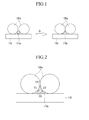
- FIGS. 1 and 2 An exemplary embodiment of a solar cell will be described with reference to FIGS. 1 and 2 .
- FIGS. 1 and 2 are schematic views of exemplary embodiments showing the conductive paste applied on the semiconductor substrate in one exemplary embodiment of a solar cell according to the present invention.
- the present invention is not limited to using the conductive paste within a solar cell and may be applied to other applications such as a PDP electrode or an OLED grid electrode.
- a conductive powder 120a and a metallic glass 115a included in the conductive paste may be present as particles, respectively.
- a glass transition temperature Tg of the metallic glass 115a is lower than an eutectic temperature of a semiconductor material, such as silicon, and the conductive powder 120a, when the conductive paste is applied on the semiconductor substrate 110 and heat-treated ( ⁇ ) at greater than a glass transition temperature Tg of the metallic glass 115a, the metallic glass 115a may be softened to fill the gap between a plurality of conductive powder 120a particles and the semiconductor substrate 110, to form a softened metallic glass 115b, as shown in FIG 1 .
- the softened metallic glass 115b may provide contact portions C1 and C2 with the conductive powder 120a, a contact portion C3 with a semiconductor substrate 110, and a contact portion C4 between neighboring particles of the conductive powder 120a to increase close contacting properties therebetween.
- the softened metallic glass closely contacts the conductive powder 120a and the semiconductor substrate 110, and thereby may provide a path for transferring electric charges generated by the semiconductor substrate 110 to the conductive powder 120a. That is, the distance between the conductive powders 120a particles or between the conductive powder 120a particles and the semiconductor substrate 110 is minimal.
- the softened metallic glass 115b may be formed as a buffer layer on the semiconductor substrate 110.
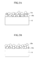
- FIGS. 3A to 3E are schematic views showing processes of providing a buffer layer on a semiconductor substrate applied with a conductive paste while increasing the temperature thereof.
- a conductive paste including the conductive powder 120a and the metallic glass 115a (here, the illustration of the organic vehicle is omitted) is applied on a semiconductor substrate 110.
- the temperature is increased to a temperature higher than the glass transition temperature Tg of the metallic glass 115a.
- the glass transition temperature Tg may range from about 450° C to about 500° C.
- the metallic glass 115b that is softened at a higher temperature than the glass transition temperature Tg may have wettability to contact the semiconductor substrate 110, and therefore closely contacts the semiconductor substrate 110.
- the softened metallic glass 115b has low viscosity, it may have high wettability, and therefore may increase the close contacting property thereof.
- the temperature is increased to a temperature higher than a sintering temperature Ts of the conductive powder 120a.
- the sintering temperature Ts may range from about 580° C to about 700° C.
- the adjacent conductive powder 120a may provide a firmly fastened and sintered conductive powder 120b at a temperature higher than the sintering temperature Ts.
- the metallic glass may exist as a solid, a supercooled liquid, or a liquid at the sintering temperature of the conductive powder 120a.
- temperature is increased to be greater than the eutectic temperature T1 of a sintered conductive powder 120b and the softened metallic glass 115b.
- the eutectic temperature may be about 780° C.
- the conductive powder 120b and the metallic glass 115b may be an eutectic mixture having an increased close contacting property, and the first eutectic layer 117 may be disposed between them.
- FIG. 3F is an enlarged view of Section 'A' (as indicated by dashed lines) shown in FIG. 3E .
- the temperature is increased to higher than the eutectic temperature T2 of the softened metallic glass 115b and the semiconductor substrate 110.
- the eutectic temperature may be about 802° C.
- the metallic glass 115b and the semiconductor substrate 110 may be an eutectic mixture having an increased close contacting property, and the second eutectic layer 118 may be disposed between them.
- the softened metallic glass 115b may provide a buffer layer 115 by being crystallized at a certain temperature, and the buffer layer 115 may prevent the conductive powder 120b from diffusing into the semiconductor substrate 110.
- a semiconductor substrate and an electrode are electrically connected to each other using a conductive metallic glass.
- loss of electric charges is decreased by enlarging the path for transferring the electric charges to the electrode from the semiconductor substrate, and a buffer layer including the metallic glass may prevent a conductive material of the electrode from deleteriously diffusing into the semiconductor substrate.
- exemplary embodiments of the conductive paste may further include glass frit.
- the glass frit may show a similar behavior as a metallic glass to form a part of a buffer layer and an eutectic layer.
- FIG. 4 another exemplary embodiment of a solar cell according to the present invention is described in detail.
- FIG. 4 is a cross-sectional view of an exemplary embodiment of a solar cell according to the present invention.
- a solar energy incident side of a semiconductor substrate 110 is called a front side, and the opposite side is called a rear side; although alternative configurations are possible.
- the exemplary embodiment of a solar cell according to the present invention may include a semiconductor substrate 110 including a lower semiconductor layer 110a and an upper semiconductor layer 110b.
- Exemplary embodiments of the semiconductor substrate 110 may be formed of a crystalline silicon or a compound semiconductor. Exemplary embodiments of the crystalline silicon may be, for example, a silicon wafer.
- One of the lower semiconductor layer 110a and the upper semiconductor layer 110b may be a semiconductor layer doped with a p-type impurity, and the other may be a semiconductor layer doped with an n-type impurity.
- the lower semiconductor layer 110a may be a semiconductor layer doped with a p-type impurity
- the upper semiconductor layer 110b may be a semiconductor layer doped with an n-type impurity.
- the p-type impurity may be a Group III element such as boron (B)
- the n-type impurity may be a Group V element such as phosphorus (P).
- the surface of the upper semiconductor layer 110b may be subjected to surface texturing.
- the surface-textured upper semiconductor layer 110b may have protrusions and depressions such as in a pyramid shape, or a porous structure such as a honeycomb or various other similar shapes.
- the surface-textured upper semiconductor layer 110b may have an enlarged surface area to enhance the light-absorption rate and decrease reflectivity, resultantly improving efficiency of a solar cell.
- a plurality of front electrodes 120 are disposed on the semiconductor layer 110b.
- the front electrodes 120 are arranged substantially in parallel to the plane of the substrate, and may be designed in a grid pattern with respect to shadowing loss and sheet resistance of the resulting solar cell.
- the front electrode 120 may be formed of a conductive material, for example a low resistance conductive material such as silver (Ag).
- the front electrode 120 may be disposed by a screen printing process using the conductive paste as described above.
- the conductive paste includes a conductive powder, a metallic glass, and an organic vehicle.
- a buffer layer 115 is disposed between the upper semiconductor layer 110b and the front electrode 120.
- the buffer layer 115 is a layer formed by softening the metallic glass in the conductive paste at a temperature greater than a glass transition temperature Tg of the metallic glass. Since the buffer layer 115 has conductivity due to the metallic glass and has parts that contact the electrode 120 and the upper semiconductor layer 110b, it may decrease loss of electric charges by enlarging the path for transferring electric charges between the upper semiconductor layer 110b and the front electrode 120. In addition, the buffer layer 115 may prevent a material of the front electrode 120 from deleteriously diffusing into the semiconductor substrate 110.
- a first eutectic layer 117 is disposed between the front electrode 120 and the buffer layer 115, and a second eutectic layer 118 is disposed between the buffer layer 115 and the upper semiconductor layer 110b.
- the first eutectic layer 117 includes an eutectic mixture of the conductive material included in the front electrode 120 and the metallic glass included in the buffer layer 115
- the second eutectic layer 118 includes an eutectic mixture of the metallic glass included in the buffer layer 115 and the semiconductor material included in the upper semiconductor layer 110b.
- a bus bar electrode (not shown) may be disposed on the front electrode 120.
- the bus bar electrode connects adjacent solar cells during assembly of a plurality of solar cells.
- a dielectric layer 130 is disposed under the semiconductor substrate 110.
- the dielectric layer 130 may increase efficiency of a solar cell by preventing recombination of electric charges and leaking of a current.
- the dielectric layer 130 may include a plurality of penetration parts 135, and the semiconductor substrate 110 and a rear electrode 140 that will be described in more detail below may contact one another through the penetration parts 135.
- the dielectric layer 130 may be formed with silicon oxide (SiO 2 ), silicon nitride (SiN x ), aluminum oxide (Al 2 O 3 ), a combination thereof or other materials with similar characteristics, and may have a thickness of about 100 ⁇ to about 2000 ⁇ .
- a rear electrode 140 is disposed under the dielectric layer 130.
- the rear electrode 140 may be formed of a conductive material, and in one exemplary embodiment it may be an opaque metal such as aluminum (Al).
- the rear electrode 140 may be disposed by a screen printing process using the above-mentioned conductive paste in the same manner as the front electrode 120.
- a buffer layer (not shown) is disposed between the rear electrode 140 and the lower semiconductor layer 110a in the same manner as the front electrode 120. Further, a first eutectic layer (not shown) is disposed between the rear electrode 140 and the buffer layer, and a second eutectic layer (not shown) is disposed between the lower semiconductor layer 110b and the buffer layer in the same manner as the front electrode 120.
- a semiconductor substrate 110 such as a silicon wafer is prepared.
- the semiconductor substrate 110 may be doped with a p-type impurity.
- the semiconductor substrate 110 is subjected to a surface texturing treatment.
- a surface texturing treatment may be performed by a wet method using a strong acid such as nitric acid and hydrofluoric acid or a strong base such as sodium hydroxide, or by a dry method using plasma.
- the semiconductor substrate 110 may be doped with an n-type impurity.
- the n-type impurity may be doped by diffusing POCl 3 or H 3 PO 4 or the like into the semiconductor substrate 110 at a high temperature.
- the semiconductor substrate 110 includes a lower semiconductor layer 110a and an upper semiconductor layer 110b doped with different impurities from each other.
- the conductive paste for a front electrode may be provided by a screen printing method.
- the screen printing method includes applying a front electrode conductive paste including a conductive powder such as silver (Ag), a metallic glass, and an organic vehicle on the position where a front electrode is positioned, and drying the same.
- a conductive paste may include a metallic glass, and the metallic glass may be prepared using any kind of method such as melt spinning, infiltration casting, gas atomization, ion irradiation, mechanical alloying or other similar methods.
- a dielectric layer 130 may be provided by stacking aluminum oxide (Al 2 O 3 ) or silicon oxide (SiO 2 ) on the rear side of the semiconductor substrate 110, as an example, by a plasma enhanced chemical vapor deposition (“PECVD”) method or other similar methods.
- PECVD plasma enhanced chemical vapor deposition
- a plurality of penetration parts 135 may be provided on one part of the dielectric layer 130 using a laser.
- the conductive paste for forming a rear electrode is subsequently applied on one side of the dielectric layer 130, e.g., by a screen printing.
- the conductive paste for forming a rear electrode is then dried.
- the conductive paste for forming a front electrode and the conductive paste for forming a rear electrode are co-fired.
- alternative exemplary embodiments include configurations wherein the conductive paste for a front electrode and the conductive paste for a rear electrode may be respectively fired.
- the firing may be performed at a higher temperature than the melting temperature of the conductive metal in a furnace, for example at a temperature ranging from about 400° C to about 1000° C.
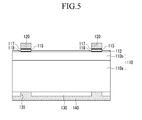
- FIG. 5 Another exemplary embodiment of a solar cell according to the present invention is described referring to FIG. 5 .
- FIG. 5 is a cross-sectional view showing another exemplary embodiment of a solar cell according to the present invention.
- an exemplary embodiment of a solar cell includes, as described with respect to the above-mentioned embodiment, a semiconductor substrate 110 including lower semiconductor layer 110a and upper semiconductor layer 110b; a plurality of front electrodes 120; a buffer layer 115 positioned between an upper semiconductor layer 110b and the front electrodes 120; a first eutectic layer 117 positioned between the front electrode 120 and the buffer layer 115; a second eutectic layer 118 positioned between the upper semiconductor layer 110b and the buffer layer 115; a dielectric layer 130 positioned under the semiconductor substrate 110; and a rear electrode 140 positioned under the dielectric layer 130.
- the solar cell according to the present embodiment unlike the above-mentioned embodiment, includes an insulating layer 112 covering the entire surface of the semiconductor substrate 110 except the regions corresponding to the buffer layer 115 as described in more detail below.
- Exemplary embodiments of the insulating layer 112 may be made of insulating material that absorbs relatively little light, for example, silicon nitride (SiN x ), silicon oxide (SiO 2 ), titanium oxide (TiO 2 ), aluminum oxide (Al 2 O 3 ), magnesium oxide (MgO), cerium oxide (CeO 2 ), a combination thereof, or other materials with similar characteristics.
- Exemplary embodiments of the insulating layer 112 include a single layer configuration and a multiple layer configuration.
- the insulating layer 112 may have a thickness ranging from about 200 ⁇ to about 1500 ⁇ .
- the insulating layer 112 may decrease the reflection rate of light and increase selectivity of a particular wavelength or a particular range of wavelengths on the front side of the solar cell to serve as an anti-reflective coating ("ARC").
- the insulating layer 112 may be manufactured from a material that is effective to improve its contact properties with the silicon in the surface of the semiconductor substrate 110, thereby increasing the efficiency of the solar cell.
- the front electrodes 120 may penetrate the insulating layer 112 to contact the upper semiconductor layer 110b.
- the contacting part of the front electrode 120 and the upper semiconductor layer 110b may be removed by etching, and the etching may be carried out by using the conductive paste further including glass frit with the conductive powder, the metallic glass and the organic vehicle.
- the glass frit may have an etching property with respect to the insulating layer 112.
- the glass frit may act as the metallic glass, and by further including the glass frit with metallic glass, it may improve adhesion to a lower layer.
- FIG. 6 Another exemplary embodiment of a solar cell according to the present invention is described referring to FIG. 6 .
- FIG. 6 is a cross-sectional view showing another exemplary embodiment of a solar cell according to the present invention.
- the present exemplary embodiment of a solar cell may include a semiconductor substrate 110 doped with a p-type or an n-type impurity.
- the semiconductor substrate 110 may include a plurality of first doping regions 111a and second doping regions 111b that are provided on the rear side and are doped with different impurities from each other.
- the first doping regions 111a may be doped with an n-type impurity
- the second doping regions 111b may be doped with a p-type impurity.
- the first doping regions 111a and the second doping regions 111b may be alternately disposed in the rear side of the semiconductor substrate 110.
- the front side of the semiconductor substrate 110 may be surface-textured, and therefore may enhance the light-absorption rate and decrease the reflectivity thereof, resultantly improving efficiency of a resulting solar cell.
- an insulation layer 112 is provided on the semiconductor substrate 110.
- a dielectric layer 150 including a plurality of penetration parts may be disposed on the rear side of the semiconductor substrate 110.
- the first electrode 121 connected with the first doping region 111a and the second electrode 141 connected with the second doping region 111b are disposed on the rear side of the semiconductor substrate 110, respectively.
- the first electrode 121 and the first doping region 111a may be contacted with one another through a penetration part
- the second electrode 141 and the second doping region 111b may be contacted with one another through a penetration part.
- the first electrode 121 and the second electrode 141 may be alternately disposed with one another.
- the first electrode 121 and the second electrode 141 may be disposed on the semiconductor 110 using a conductive paste including a conductive powder, a metallic glass, an organic vehicle, and optionally glass frit, which is substantially the same as described above.
- a buffer layer 115 is disposed between the first doping region 111a and the first electrode 121, and/or between the second doping region 111b and the second electrode 141.
- the buffer layer 115 may have conductivity due to a metallic glass used in the formation thereof. Since the buffer layer 115 includes parts contacting the first electrode 121 and/or the second electrode 141 and parts contacting the first doping region 111a and/or the second doping region 111b, loss of electric charges may decrease by enlarging the path for charge transfer between the first doping region 111a and the first electrode 121, and/or between the second doping region 111b and the second electrode 141. In addition, the buffer layer 115 may prevent a material of the first electrode 121 or the second electrode 141 from deleteriously diffusing into the first or second doping region 111a or 111b.
- An exemplary embodiment of a solar cell including both of the first electrode 121 and the second electrode 141 on the rear surface of the solar cell may decrease an area where a metal is positioned on the front, i.e., light incident, surface of the solar cell. This may decrease shadowing loss and increase solar cell efficiency.
- a semiconductor substrate 110 doped with, for example, an n-type impurity is prepared. Then, the semiconductor substrate 110 is surface-textured, and insulation layer 112 and dielectric layer 150 are disposed on front side and rear side of the semiconductor substrate 110, respectively.
- the insulation layer 112 and the dielectric layer 150 may be provided by chemical vapor deposition ("CVD").
- a part of the dielectric layer 150 is removed by, for example, using a laser to form a plurality of openings.
- the first doping region 111a and the second doping region 111b may be disposed by sequentially doping a p-type impurity and an n-type impurity at a high concentration in the openings at rear side of the semiconductor substrate 110.
- a conductive paste for forming a first electrode 121 is applied on one side of the dielectric layer 150 corresponding to the first doping region 111a, and a conductive paste for forming a second electrode is applied on the other side corresponding to the second doping region 111b.
- the conductive paste for forming a first electrode and the conductive paste for forming a second electrode are provided by a screen printing process, and the conductive paste including a conductive powder, a metallic glass, an organic vehicle, and optionally glass frit may be respectively used.
- the conductive paste for forming a front electrode and the conductive paste for forming a rear electrode may be fired together or respectively.
- the firing may be performed at a higher temperature than the melting temperature of a conductive metal in a furnace.
Applications Claiming Priority (2)
| Application Number | Priority Date | Filing Date | Title |
|---|---|---|---|
| KR20090108674 | 2009-11-11 | ||
| KR1020100096382A KR102071006B1 (ko) | 2009-11-11 | 2010-10-04 | 도전성 페이스트 및 태양 전지 |
Publications (3)
| Publication Number | Publication Date |
|---|---|
| EP2325848A2 true EP2325848A2 (de) | 2011-05-25 |
| EP2325848A3 EP2325848A3 (de) | 2011-09-07 |
| EP2325848B1 EP2325848B1 (de) | 2017-07-19 |
Family
ID=43629384
Family Applications (1)
| Application Number | Title | Priority Date | Filing Date |
|---|---|---|---|
| EP10190652.7A Active EP2325848B1 (de) | 2009-11-11 | 2010-11-10 | Leitfähige Paste und Solarzelle |
Country Status (4)
| Country | Link |
|---|---|
| US (1) | US9984787B2 (de) |
| EP (1) | EP2325848B1 (de) |
| JP (1) | JP2011103301A (de) |
| CN (1) | CN102097153A (de) |
Cited By (14)
| Publication number | Priority date | Publication date | Assignee | Title |
|---|---|---|---|---|
| EP2416327A1 (de) * | 2010-08-05 | 2012-02-08 | Samsung Electronics Co., Ltd. | Leitfähige Paste und elektronische Vorrichtung und Solarzelle mit einer anhand der leitfähigen Paste hergestellten Elektrode |
| KR20120044218A (ko) * | 2010-10-27 | 2012-05-07 | 삼성전자주식회사 | 도전성 페이스트 및 태양 전지 |
| EP2448003A3 (de) * | 2010-10-27 | 2012-08-08 | Samsung Electronics Co., Ltd. | Leitfähige Paste enthaltend ein leitfähiges Pulver und ein metallisches Glas zur Herstellung einer Solarzellenelektrode |
| WO2013070049A1 (en) * | 2011-11-11 | 2013-05-16 | Samsung Electronics Co., Ltd. | Conductive paste and electronic device and solar cell including an electrode formed using the conductive paste |
| US8668847B2 (en) | 2010-08-13 | 2014-03-11 | Samsung Electronics Co., Ltd. | Conductive paste and electronic device and solar cell including an electrode formed using the conductive paste |
| US8940195B2 (en) | 2011-01-13 | 2015-01-27 | Samsung Electronics Co., Ltd. | Conductive paste, and electronic device and solar cell including an electrode formed using the same |
| US8987586B2 (en) | 2010-08-13 | 2015-03-24 | Samsung Electronics Co., Ltd. | Conductive paste and electronic device and solar cell including an electrode formed using the conductive paste |
| US9039940B2 (en) | 2011-03-25 | 2015-05-26 | Samsung Electronics Co., Ltd. | Conductive paste and electronic device, and solar cell including an electrode formed using the conductive paste |
| US9105370B2 (en) | 2011-01-12 | 2015-08-11 | Samsung Electronics Co., Ltd. | Conductive paste, and electronic device and solar cell including an electrode formed using the same |
| US9115200B2 (en) | 2010-02-04 | 2015-08-25 | Toray Industries, Inc. | Pharmaceutical composition for treating cancer using a monoclonal antibody having immunological reactivity with CAPRIN-1 |
| US9218898B2 (en) | 2011-12-09 | 2015-12-22 | Samsung Electronics Co., Ltd. | Conductive paste and electronic device and solar cell including an electrode formed using the conductive paste |
| US10074752B2 (en) | 2012-06-27 | 2018-09-11 | Samsung Electronics Co., Ltd. | Conductive paste and electronic device and solar cell |
| EP2450908B1 (de) * | 2010-08-13 | 2019-07-03 | Samsung Electronics Co., Ltd. | Leitfähige Paste, Elektrode und elektronische Vorrichtung sowie Solarzelle mit einer anhand der leitfähigen Paste hergestellten Elektrode |
| US11482634B1 (en) | 2021-04-26 | 2022-10-25 | Zhejiang Jinko Solar Co., Ltd. | Photovoltaic cell, method for manufacturing same and photovoltaic module |
Families Citing this family (26)
| Publication number | Priority date | Publication date | Assignee | Title |
|---|---|---|---|---|
| KR101796658B1 (ko) * | 2011-03-28 | 2017-11-13 | 삼성전자주식회사 | 도전성 페이스트, 상기 도전성 페이스트를 사용하여 형성된 전극을 포함하는 전자 소자 및 태양 전지 |
| TWI535043B (zh) * | 2011-06-29 | 2016-05-21 | 國立屏東科技大學 | 以活性焊料製做的太陽能電池電極及其方法 |
| JP5844091B2 (ja) * | 2011-08-26 | 2016-01-13 | 横浜ゴム株式会社 | 導電性組成物、太陽電池セルおよび太陽電池モジュール |
| KR101278441B1 (ko) * | 2011-08-31 | 2013-07-01 | 한화케미칼 주식회사 | 일 단계 도핑공정을 이용한 ewt 태양전지의 제조방법 |
| KR20130027784A (ko) * | 2011-09-08 | 2013-03-18 | 삼성전기주식회사 | 외부 전극용 도전성 페이스트, 이를 이용한 적층 세라믹 전자부품 및 이의 제조방법 |
| JP6068474B2 (ja) * | 2011-09-09 | 2017-01-25 | ヘレウス プレシャス メタルズ ノース アメリカ コンショホーケン エルエルシー | 銀製の太陽電池接点 |
| US20140332072A1 (en) * | 2011-12-13 | 2014-11-13 | Dow Corning Corporation | Photovoltaic Cell And Method Of Forming The Same |
| WO2013096715A1 (en) * | 2011-12-22 | 2013-06-27 | Ferro Corporation | Solar cell pastes for low resistance contacts |
| US20130160834A1 (en) * | 2011-12-27 | 2013-06-27 | E.I. Du Pont De Nemours And Company | Back-side electrode of p-type solar cell, and method for forming the same |
| CN102426873B (zh) * | 2011-12-28 | 2014-12-10 | 彩虹集团公司 | 硅太阳能电池正银浆料及其制备方法 |
| US9153712B2 (en) * | 2012-09-27 | 2015-10-06 | Sunpower Corporation | Conductive contact for solar cell |
| KR20140050390A (ko) * | 2012-10-19 | 2014-04-29 | 삼성전자주식회사 | 열전모듈, 이를 구비한 열전장치, 및 열전모듈의 제조방법 |
| US20140158192A1 (en) * | 2012-12-06 | 2014-06-12 | Michael Cudzinovic | Seed layer for solar cell conductive contact |
| TWI489636B (zh) * | 2013-03-13 | 2015-06-21 | Neo Solar Power Corp | 具有金屬堆疊電極之太陽能電池及其製造方法 |
| KR101648242B1 (ko) * | 2013-03-27 | 2016-08-12 | 제일모직주식회사 | 태양전지 전극 형성용 조성물 및 이로부터 제조된 전극 |
| KR20150066133A (ko) * | 2013-12-06 | 2015-06-16 | 삼성전자주식회사 | 금속 유리의 분쇄 방법, 분쇄된 금속 유리, 도전성 페이스트 및 전자 소자 |
| US20160163901A1 (en) * | 2014-12-08 | 2016-06-09 | Benjamin Ian Hsia | Laser stop layer for foil-based metallization of solar cells |
| US20160229552A1 (en) * | 2015-02-05 | 2016-08-11 | The Boeing Company | Intermetallic and composite metallic gap filler |
| WO2016156221A1 (en) * | 2015-03-27 | 2016-10-06 | Heraeus Deutschland Gmbh & Co Kg | Electro-conductive pastes comprising an organic metal oxide |
| US20170226619A1 (en) * | 2016-02-09 | 2017-08-10 | California Institute Of Technology | Systems and Methods Implementing Layers of Devitrified Metallic Glass-Based Materials |
| US20180226533A1 (en) * | 2017-02-08 | 2018-08-09 | Amberwave Inc. | Thin Film Solder Bond |
| CN107623765B (zh) * | 2017-08-21 | 2020-10-23 | 东莞华晶粉末冶金有限公司 | 一种具有无线充电功能的电子产品陶瓷后盖及制造方法 |
| CN107801298A (zh) * | 2017-12-01 | 2018-03-13 | 绵阳市奇帆科技有限公司 | Pcb线路板印刷铜浆 |
| KR20190068351A (ko) * | 2017-12-08 | 2019-06-18 | 삼성에스디아이 주식회사 | 태양전지 셀 |
| CN109273137B (zh) * | 2018-09-30 | 2021-11-19 | 东莞市银屏电子科技有限公司 | 一种太阳能hit电池用低温导电银浆及其制备方法 |
| CN112509727B (zh) * | 2020-11-10 | 2022-08-12 | 广东工业大学 | 一种用于低温共烧陶瓷的内电极铜浆及其制备方法和应用 |
Family Cites Families (62)
| Publication number | Priority date | Publication date | Assignee | Title |
|---|---|---|---|---|
| US4434084A (en) * | 1981-09-23 | 1984-02-28 | E. I. Du Pont De Nemours And Company | Base metal conductor cathode coating for tantalum capacitors |
| JPS6262870A (ja) | 1985-09-12 | 1987-03-19 | Masami Kobayashi | 電磁波遮へい塗料 |
| DE3905276C1 (de) * | 1989-02-21 | 1990-05-03 | Demetron Gesellschaft Fuer Elektronik-Werkstoffe Mbh, 6450 Hanau, De | |
| US5170930A (en) * | 1991-11-14 | 1992-12-15 | Microelectronics And Computer Technology Corporation | Liquid metal paste for thermal and electrical connections |
| US5709958A (en) | 1992-08-27 | 1998-01-20 | Kabushiki Kaisha Toshiba | Electronic parts |
| US5288344A (en) | 1993-04-07 | 1994-02-22 | California Institute Of Technology | Berylllium bearing amorphous metallic alloys formed by low cooling rates |
| JP3592006B2 (ja) | 1996-11-12 | 2004-11-24 | 松下電器産業株式会社 | ビアホール充填用導電性ペースト及びそれを用いたプリント配線板 |
| US6027575A (en) * | 1997-10-27 | 2000-02-22 | Ford Motor Company | Metallic adhesive for forming electronic interconnects at low temperatures |
| JP2000082461A (ja) * | 1998-07-06 | 2000-03-21 | Canon Inc | Mg系負極活物質、その製造法、水素吸蔵合金電極およびアルカリ二次電池 |
| JP3620703B2 (ja) | 1998-09-18 | 2005-02-16 | キヤノン株式会社 | 二次電池用負極電極材、電極構造体、二次電池、及びこれらの製造方法 |
| TW508862B (en) | 1999-09-09 | 2002-11-01 | Canon Kk | Alkali rechargeable batteries and process for the production of said rechargeable batteries |
| CA2287648C (en) | 1999-10-26 | 2007-06-19 | Donald W. Kirk | Amorphous metal/metallic glass electrodes for electrochemical processes |
| JP3918450B2 (ja) | 2000-07-05 | 2007-05-23 | 株式会社村田製作所 | 導電粉末の製造方法、導電粉末、導電性ペーストおよび積層セラミック電子部品 |
| WO2002027050A1 (en) | 2000-09-25 | 2002-04-04 | Johns Hopkins University | Alloy with metallic glass and quasi-crystalline properties |
| JP3564089B2 (ja) | 2001-01-24 | 2004-09-08 | 株式会社ノリタケカンパニーリミテド | 導体ペースト及びその製造方法 |
| JP3860445B2 (ja) | 2001-04-19 | 2006-12-20 | 独立行政法人科学技術振興機構 | Cu−Be基非晶質合金 |
| JP2003013103A (ja) | 2001-06-26 | 2003-01-15 | Murata Mfg Co Ltd | 導電粉末の製造方法、導電粉末、導電性ペーストおよび積層セラミック電子部品 |
| US20040245507A1 (en) | 2001-09-06 | 2004-12-09 | Atsushi Nagai | Conductor composition and method for production thereof |
| CN1204570C (zh) | 2002-03-01 | 2005-06-01 | 北京科技大学 | 具有超大过冷区间的稀土铁基软磁金属玻璃 |
| KR20040002317A (ko) | 2002-06-29 | 2004-01-07 | 풀무원건강생활 주식회사 | 전상온도유화 방식을 이용한 Pseudomicroemulsion의제조공정 및 조성물 |
| JP3963802B2 (ja) | 2002-08-30 | 2007-08-22 | 独立行政法人科学技術振興機構 | Cu基非晶質合金 |
| JP3913167B2 (ja) | 2002-12-25 | 2007-05-09 | 独立行政法人科学技術振興機構 | 金属ガラスからなるバルク状のFe基焼結合金軟磁性材料およびその製造方法 |
| US20070137737A1 (en) * | 2003-06-11 | 2007-06-21 | Faqiang Guo | Thermally stable calcium-aluminum bulk amorphous metals with low mass density |
| KR100677805B1 (ko) | 2003-07-23 | 2007-02-02 | 샤프 가부시키가이샤 | 은 합금 재료, 회로 기판, 전자 장치 및 회로 기판의 제조방법 |
| JP4439213B2 (ja) | 2003-07-31 | 2010-03-24 | 京セラ株式会社 | 太陽電池素子およびその製造方法 |
| JP4064340B2 (ja) | 2003-12-25 | 2008-03-19 | 昭和シェル石油株式会社 | 集積型薄膜太陽電池の製造方法 |
| KR20050087249A (ko) | 2004-02-26 | 2005-08-31 | 삼성에스디아이 주식회사 | 나노입자의 페이스트를 이용하여 형성된 전극을 포함하는태양전지 및 그 제조방법 |
| KR100583230B1 (ko) | 2004-03-29 | 2006-05-25 | 한국과학기술연구원 | 구리계 비정질 합금 조성물 |
| US20050228097A1 (en) * | 2004-03-30 | 2005-10-13 | General Electric Company | Thermally conductive compositions and methods of making thereof |
| US20060102228A1 (en) | 2004-11-12 | 2006-05-18 | Ferro Corporation | Method of making solar cell contacts |
| US7494607B2 (en) * | 2005-04-14 | 2009-02-24 | E.I. Du Pont De Nemours And Company | Electroconductive thick film composition(s), electrode(s), and semiconductor device(s) formed therefrom |
| JP2007007648A (ja) | 2005-06-30 | 2007-01-18 | Samsung Electronics Co Ltd | 分散剤、それを含むペースト組成物、及びそれを使用して製造される無機素子、並びにそれを含むディスプレイ装置 |
| US7628871B2 (en) * | 2005-08-12 | 2009-12-08 | Intel Corporation | Bulk metallic glass solder material |
| KR101178053B1 (ko) | 2005-09-27 | 2012-08-30 | 삼성전자주식회사 | 카르복실 에스테르계 분산제 및 그를 포함하는 황화물계 형광체 페이스트 조성물 |
| KR101146667B1 (ko) | 2005-11-07 | 2012-05-24 | 삼성에스디아이 주식회사 | 금속산화물 페이스트 조성물 및 그를 이용한 반도체 전극의제조방법 |
| US8575474B2 (en) * | 2006-03-20 | 2013-11-05 | Heracus Precious Metals North America Conshohocken LLC | Solar cell contacts containing aluminum and at least one of boron, titanium, nickel, tin, silver, gallium, zinc, indium and copper |
| KR100784914B1 (ko) | 2006-05-01 | 2007-12-11 | 학교법인연세대학교 | 다단계 변형이 가능한 이상분리 비정질 합금 |
| JP2008010527A (ja) | 2006-06-28 | 2008-01-17 | Sharp Corp | 太陽電池電極用導電性ペースト |
| TWI399759B (zh) | 2006-06-30 | 2013-06-21 | Mitsubishi Materials Corp | 形成太陽電池之電極用組成物及該電極之形成方法以及使用依該形成方法所得電極之太陽電池 |
| US20100096014A1 (en) | 2006-12-25 | 2010-04-22 | Hideyo Iida | Conductive paste for solar cell |
| US20080196794A1 (en) | 2007-02-20 | 2008-08-21 | Centre National De La Recherche Scientifique Institut National Polytechnique De Grenoble | Bulk metallic glass/metal composites produced by codeformation |
| US9580810B2 (en) | 2007-02-27 | 2017-02-28 | Mitsubishi Materials Corporation | Dispersion of metal nanoparticles, method for producing the same, and method for synthesizing metal nanoparticles |
| WO2008124623A1 (en) * | 2007-04-04 | 2008-10-16 | California Institute Of Technology | Process for joining materials using bulk metallic glasses |
| US8309844B2 (en) * | 2007-08-29 | 2012-11-13 | Ferro Corporation | Thick film pastes for fire through applications in solar cells |
| JP2009099371A (ja) | 2007-10-17 | 2009-05-07 | Sanyo Special Steel Co Ltd | 燃料電池用電極の製造方法 |
| CN101186128A (zh) * | 2007-10-29 | 2008-05-28 | 福建师范大学 | 一种耐高温高光学反射的导电薄膜及其制备方法 |
| JP2009138266A (ja) | 2007-11-16 | 2009-06-25 | Sanyo Special Steel Co Ltd | 高密度かつ非晶質の金属ガラス粉末焼結体の製造方法およびその焼結体 |
| JP5332624B2 (ja) | 2008-01-22 | 2013-11-06 | 三菱マテリアル株式会社 | 金属ナノ粒子分散液及びその製造方法 |
| KR101448448B1 (ko) | 2008-02-20 | 2014-10-14 | 주성엔지니어링(주) | 박막형 태양전지 및 그 제조방법 |
| US20090211626A1 (en) * | 2008-02-26 | 2009-08-27 | Hideki Akimoto | Conductive paste and grid electrode for silicon solar cells |
| EP2107136B1 (de) | 2008-03-31 | 2014-12-31 | Permelec Electrode Ltd. | Herstellungsverfahren für Elektroden für Elektrolyse |
| US8158504B2 (en) | 2008-05-30 | 2012-04-17 | E. I. Du Pont De Nemours And Company | Conductive compositions and processes for use in the manufacture of semiconductor devices—organic medium components |
| EP2342756A4 (de) | 2008-06-09 | 2012-10-17 | Sdsu Res Foundation | Organische photovoltaische zelle und lichtemittierende diode mit einem array aus dreidimensional hergestellten elektroden |
| JP5224514B2 (ja) | 2008-07-14 | 2013-07-03 | 国立大学法人東北大学 | ナノサイズ金属ガラス構造体 |
| CN101359564B (zh) * | 2008-09-16 | 2011-08-17 | 彩虹集团公司 | 抗Ag扩散感光性导电浆料及其制备方法 |
| TWI423462B (zh) | 2008-10-22 | 2014-01-11 | Ind Tech Res Inst | 矽晶太陽電池之背面電極製造方法 |
| JP2010133021A (ja) | 2008-10-31 | 2010-06-17 | Topy Ind Ltd | 溶射用粒子 |
| JP5326647B2 (ja) | 2009-02-24 | 2013-10-30 | 三菱マテリアル株式会社 | 太陽電池の電極形成用組成物の製造方法 |
| KR101741683B1 (ko) | 2010-08-05 | 2017-05-31 | 삼성전자주식회사 | 도전성 페이스트, 상기 도전성 페이스트를 사용하여 형성된 전극을 포함하는 전자 소자 및 태양 전지 |
| US8668847B2 (en) | 2010-08-13 | 2014-03-11 | Samsung Electronics Co., Ltd. | Conductive paste and electronic device and solar cell including an electrode formed using the conductive paste |
| CN102376379B (zh) | 2010-08-13 | 2016-04-20 | 三星电子株式会社 | 导电糊料及包含用其形成的电极的电子器件和太阳能电池 |
| EP2448003A3 (de) | 2010-10-27 | 2012-08-08 | Samsung Electronics Co., Ltd. | Leitfähige Paste enthaltend ein leitfähiges Pulver und ein metallisches Glas zur Herstellung einer Solarzellenelektrode |
-
2010
- 2010-11-10 EP EP10190652.7A patent/EP2325848B1/de active Active
- 2010-11-10 US US12/943,732 patent/US9984787B2/en active Active
- 2010-11-11 CN CN201010544709XA patent/CN102097153A/zh active Pending
- 2010-11-11 JP JP2010252993A patent/JP2011103301A/ja active Pending
Non-Patent Citations (1)
| Title |
|---|
| None |
Cited By (19)
| Publication number | Priority date | Publication date | Assignee | Title |
|---|---|---|---|---|
| US9947809B2 (en) | 2009-11-11 | 2018-04-17 | Samsung Electronics Co., Ltd. | Conductive paste and electronic device and solar cell including an electrode formed using the conductive paste |
| US9115200B2 (en) | 2010-02-04 | 2015-08-25 | Toray Industries, Inc. | Pharmaceutical composition for treating cancer using a monoclonal antibody having immunological reactivity with CAPRIN-1 |
| US8715535B2 (en) | 2010-08-05 | 2014-05-06 | Samsung Electronics Co., Ltd. | Conductive paste and electronic device and solar cell including an electrode formed using the conductive paste |
| EP2416327A1 (de) * | 2010-08-05 | 2012-02-08 | Samsung Electronics Co., Ltd. | Leitfähige Paste und elektronische Vorrichtung und Solarzelle mit einer anhand der leitfähigen Paste hergestellten Elektrode |
| US8987586B2 (en) | 2010-08-13 | 2015-03-24 | Samsung Electronics Co., Ltd. | Conductive paste and electronic device and solar cell including an electrode formed using the conductive paste |
| US8668847B2 (en) | 2010-08-13 | 2014-03-11 | Samsung Electronics Co., Ltd. | Conductive paste and electronic device and solar cell including an electrode formed using the conductive paste |
| EP2450908B1 (de) * | 2010-08-13 | 2019-07-03 | Samsung Electronics Co., Ltd. | Leitfähige Paste, Elektrode und elektronische Vorrichtung sowie Solarzelle mit einer anhand der leitfähigen Paste hergestellten Elektrode |
| KR20120044218A (ko) * | 2010-10-27 | 2012-05-07 | 삼성전자주식회사 | 도전성 페이스트 및 태양 전지 |
| EP2448003A3 (de) * | 2010-10-27 | 2012-08-08 | Samsung Electronics Co., Ltd. | Leitfähige Paste enthaltend ein leitfähiges Pulver und ein metallisches Glas zur Herstellung einer Solarzellenelektrode |
| US8974703B2 (en) | 2010-10-27 | 2015-03-10 | Samsung Electronics Co., Ltd. | Conductive paste and electronic device and solar cell including an electrode formed using the same |
| US9105370B2 (en) | 2011-01-12 | 2015-08-11 | Samsung Electronics Co., Ltd. | Conductive paste, and electronic device and solar cell including an electrode formed using the same |
| US8940195B2 (en) | 2011-01-13 | 2015-01-27 | Samsung Electronics Co., Ltd. | Conductive paste, and electronic device and solar cell including an electrode formed using the same |
| US9039940B2 (en) | 2011-03-25 | 2015-05-26 | Samsung Electronics Co., Ltd. | Conductive paste and electronic device, and solar cell including an electrode formed using the conductive paste |
| WO2013070049A1 (en) * | 2011-11-11 | 2013-05-16 | Samsung Electronics Co., Ltd. | Conductive paste and electronic device and solar cell including an electrode formed using the conductive paste |
| EP2777049A4 (de) * | 2011-11-11 | 2016-06-15 | Samsung Electronics Co Ltd | Leitfähige paste sowie elektronische vorrichtung und solarzelle mit einer aus der leitfähigen paste geformten elektrode |
| US9218898B2 (en) | 2011-12-09 | 2015-12-22 | Samsung Electronics Co., Ltd. | Conductive paste and electronic device and solar cell including an electrode formed using the conductive paste |
| US10074752B2 (en) | 2012-06-27 | 2018-09-11 | Samsung Electronics Co., Ltd. | Conductive paste and electronic device and solar cell |
| US11482634B1 (en) | 2021-04-26 | 2022-10-25 | Zhejiang Jinko Solar Co., Ltd. | Photovoltaic cell, method for manufacturing same and photovoltaic module |
| EP4084086A1 (de) * | 2021-04-26 | 2022-11-02 | Zhejiang Jinko Solar Co., Ltd. | Photovoltaische zelle, herstellungsverfahren dafür und photovoltaisches modul |
Also Published As
| Publication number | Publication date |
|---|---|
| EP2325848B1 (de) | 2017-07-19 |
| EP2325848A3 (de) | 2011-09-07 |
| US20110114170A1 (en) | 2011-05-19 |
| US9984787B2 (en) | 2018-05-29 |
| CN102097153A (zh) | 2011-06-15 |
| JP2011103301A (ja) | 2011-05-26 |
Similar Documents
| Publication | Publication Date | Title |
|---|---|---|
| EP2325848B1 (de) | Leitfähige Paste und Solarzelle | |
| KR102035253B1 (ko) | 도전성 페이스트 및 태양 전지 | |
| US8715535B2 (en) | Conductive paste and electronic device and solar cell including an electrode formed using the conductive paste | |
| EP2450908B1 (de) | Leitfähige Paste, Elektrode und elektronische Vorrichtung sowie Solarzelle mit einer anhand der leitfähigen Paste hergestellten Elektrode | |
| US8974703B2 (en) | Conductive paste and electronic device and solar cell including an electrode formed using the same | |
| US8668847B2 (en) | Conductive paste and electronic device and solar cell including an electrode formed using the conductive paste | |
| US9947809B2 (en) | Conductive paste and electronic device and solar cell including an electrode formed using the conductive paste | |
| US9039940B2 (en) | Conductive paste and electronic device, and solar cell including an electrode formed using the conductive paste | |
| US20130104973A1 (en) | Conductive paste, and electronic device and solar cell including electrode formed using the conductive paste | |
| KR101741682B1 (ko) | 도전성 페이스트와 상기 도전성 페이스트를 사용하여 형성된 전극을 포함하는 전자 소자 및 태양 전지 | |
| US9105370B2 (en) | Conductive paste, and electronic device and solar cell including an electrode formed using the same | |
| US20100319766A1 (en) | Solar cell and method for manufacturing the same | |
| US8987586B2 (en) | Conductive paste and electronic device and solar cell including an electrode formed using the conductive paste | |
| US9039943B2 (en) | Conductive paste and electronic device and solar cell including an electrode formed using the conductive paste | |
| KR20130065446A (ko) | 태양 전지 | |
| KR101960466B1 (ko) | 도전성 페이스트, 상기 도전성 페이스트를 사용하여 형성된 전극을 포함하는 전자 소자 및 태양 전지 |
Legal Events
| Date | Code | Title | Description |
|---|---|---|---|
| PUAI | Public reference made under article 153(3) epc to a published international application that has entered the european phase |
Free format text: ORIGINAL CODE: 0009012 |
|
| AK | Designated contracting states |
Kind code of ref document: A2 Designated state(s): AL AT BE BG CH CY CZ DE DK EE ES FI FR GB GR HR HU IE IS IT LI LT LU LV MC MK MT NL NO PL PT RO RS SE SI SK SM TR |
|
| AX | Request for extension of the european patent |
Extension state: BA ME |
|
| PUAL | Search report despatched |
Free format text: ORIGINAL CODE: 0009013 |
|
| AK | Designated contracting states |
Kind code of ref document: A3 Designated state(s): AL AT BE BG CH CY CZ DE DK EE ES FI FR GB GR HR HU IE IS IT LI LT LU LV MC MK MT NL NO PL PT RO RS SE SI SK SM TR |
|
| AX | Request for extension of the european patent |
Extension state: BA ME |
|
| RIC1 | Information provided on ipc code assigned before grant |
Ipc: H01B 1/22 20060101AFI20110729BHEP Ipc: H01L 31/0224 20060101ALI20110729BHEP |
|
| 17P | Request for examination filed |
Effective date: 20120305 |
|
| RAP1 | Party data changed (applicant data changed or rights of an application transferred) |
Owner name: SAMSUNG ELECTRONICS CO., LTD. |
|
| 17Q | First examination report despatched |
Effective date: 20160504 |
|
| GRAP | Despatch of communication of intention to grant a patent |
Free format text: ORIGINAL CODE: EPIDOSNIGR1 |
|
| INTG | Intention to grant announced |
Effective date: 20170203 |
|
| GRAS | Grant fee paid |
Free format text: ORIGINAL CODE: EPIDOSNIGR3 |
|
| GRAA | (expected) grant |
Free format text: ORIGINAL CODE: 0009210 |
|
| AK | Designated contracting states |
Kind code of ref document: B1 Designated state(s): AL AT BE BG CH CY CZ DE DK EE ES FI FR GB GR HR HU IE IS IT LI LT LU LV MC MK MT NL NO PL PT RO RS SE SI SK SM TR |
|
| REG | Reference to a national code |
Ref country code: GB Ref legal event code: FG4D |
|
| REG | Reference to a national code |
Ref country code: CH Ref legal event code: EP |
|
| REG | Reference to a national code |
Ref country code: IE Ref legal event code: FG4D |
|
| REG | Reference to a national code |
Ref country code: AT Ref legal event code: REF Ref document number: 911100 Country of ref document: AT Kind code of ref document: T Effective date: 20170815 |
|
| REG | Reference to a national code |
Ref country code: DE Ref legal event code: R096 Ref document number: 602010043689 Country of ref document: DE |
|
| REG | Reference to a national code |
Ref country code: FR Ref legal event code: PLFP Year of fee payment: 8 |
|
| REG | Reference to a national code |
Ref country code: NL Ref legal event code: MP Effective date: 20170719 |
|
| REG | Reference to a national code |
Ref country code: LT Ref legal event code: MG4D |
|
| REG | Reference to a national code |
Ref country code: AT Ref legal event code: MK05 Ref document number: 911100 Country of ref document: AT Kind code of ref document: T Effective date: 20170719 |
|
| PG25 | Lapsed in a contracting state [announced via postgrant information from national office to epo] |
Ref country code: LT Free format text: LAPSE BECAUSE OF FAILURE TO SUBMIT A TRANSLATION OF THE DESCRIPTION OR TO PAY THE FEE WITHIN THE PRESCRIBED TIME-LIMIT Effective date: 20170719 Ref country code: NO Free format text: LAPSE BECAUSE OF FAILURE TO SUBMIT A TRANSLATION OF THE DESCRIPTION OR TO PAY THE FEE WITHIN THE PRESCRIBED TIME-LIMIT Effective date: 20171019 Ref country code: NL Free format text: LAPSE BECAUSE OF FAILURE TO SUBMIT A TRANSLATION OF THE DESCRIPTION OR TO PAY THE FEE WITHIN THE PRESCRIBED TIME-LIMIT Effective date: 20170719 Ref country code: HR Free format text: LAPSE BECAUSE OF FAILURE TO SUBMIT A TRANSLATION OF THE DESCRIPTION OR TO PAY THE FEE WITHIN THE PRESCRIBED TIME-LIMIT Effective date: 20170719 Ref country code: SE Free format text: LAPSE BECAUSE OF FAILURE TO SUBMIT A TRANSLATION OF THE DESCRIPTION OR TO PAY THE FEE WITHIN THE PRESCRIBED TIME-LIMIT Effective date: 20170719 Ref country code: FI Free format text: LAPSE BECAUSE OF FAILURE TO SUBMIT A TRANSLATION OF THE DESCRIPTION OR TO PAY THE FEE WITHIN THE PRESCRIBED TIME-LIMIT Effective date: 20170719 Ref country code: AT Free format text: LAPSE BECAUSE OF FAILURE TO SUBMIT A TRANSLATION OF THE DESCRIPTION OR TO PAY THE FEE WITHIN THE PRESCRIBED TIME-LIMIT Effective date: 20170719 |
|
| PG25 | Lapsed in a contracting state [announced via postgrant information from national office to epo] |
Ref country code: LV Free format text: LAPSE BECAUSE OF FAILURE TO SUBMIT A TRANSLATION OF THE DESCRIPTION OR TO PAY THE FEE WITHIN THE PRESCRIBED TIME-LIMIT Effective date: 20170719 Ref country code: RS Free format text: LAPSE BECAUSE OF FAILURE TO SUBMIT A TRANSLATION OF THE DESCRIPTION OR TO PAY THE FEE WITHIN THE PRESCRIBED TIME-LIMIT Effective date: 20170719 Ref country code: ES Free format text: LAPSE BECAUSE OF FAILURE TO SUBMIT A TRANSLATION OF THE DESCRIPTION OR TO PAY THE FEE WITHIN THE PRESCRIBED TIME-LIMIT Effective date: 20170719 Ref country code: IS Free format text: LAPSE BECAUSE OF FAILURE TO SUBMIT A TRANSLATION OF THE DESCRIPTION OR TO PAY THE FEE WITHIN THE PRESCRIBED TIME-LIMIT Effective date: 20171119 Ref country code: BG Free format text: LAPSE BECAUSE OF FAILURE TO SUBMIT A TRANSLATION OF THE DESCRIPTION OR TO PAY THE FEE WITHIN THE PRESCRIBED TIME-LIMIT Effective date: 20171019 Ref country code: GR Free format text: LAPSE BECAUSE OF FAILURE TO SUBMIT A TRANSLATION OF THE DESCRIPTION OR TO PAY THE FEE WITHIN THE PRESCRIBED TIME-LIMIT Effective date: 20171020 Ref country code: PL Free format text: LAPSE BECAUSE OF FAILURE TO SUBMIT A TRANSLATION OF THE DESCRIPTION OR TO PAY THE FEE WITHIN THE PRESCRIBED TIME-LIMIT Effective date: 20170719 |
|
| REG | Reference to a national code |
Ref country code: DE Ref legal event code: R097 Ref document number: 602010043689 Country of ref document: DE |
|
| PG25 | Lapsed in a contracting state [announced via postgrant information from national office to epo] |
Ref country code: RO Free format text: LAPSE BECAUSE OF FAILURE TO SUBMIT A TRANSLATION OF THE DESCRIPTION OR TO PAY THE FEE WITHIN THE PRESCRIBED TIME-LIMIT Effective date: 20170719 Ref country code: DK Free format text: LAPSE BECAUSE OF FAILURE TO SUBMIT A TRANSLATION OF THE DESCRIPTION OR TO PAY THE FEE WITHIN THE PRESCRIBED TIME-LIMIT Effective date: 20170719 Ref country code: CZ Free format text: LAPSE BECAUSE OF FAILURE TO SUBMIT A TRANSLATION OF THE DESCRIPTION OR TO PAY THE FEE WITHIN THE PRESCRIBED TIME-LIMIT Effective date: 20170719 |
|
| PLBE | No opposition filed within time limit |
Free format text: ORIGINAL CODE: 0009261 |
|
| STAA | Information on the status of an ep patent application or granted ep patent |
Free format text: STATUS: NO OPPOSITION FILED WITHIN TIME LIMIT |
|
| PG25 | Lapsed in a contracting state [announced via postgrant information from national office to epo] |
Ref country code: EE Free format text: LAPSE BECAUSE OF FAILURE TO SUBMIT A TRANSLATION OF THE DESCRIPTION OR TO PAY THE FEE WITHIN THE PRESCRIBED TIME-LIMIT Effective date: 20170719 Ref country code: IT Free format text: LAPSE BECAUSE OF FAILURE TO SUBMIT A TRANSLATION OF THE DESCRIPTION OR TO PAY THE FEE WITHIN THE PRESCRIBED TIME-LIMIT Effective date: 20170719 Ref country code: SK Free format text: LAPSE BECAUSE OF FAILURE TO SUBMIT A TRANSLATION OF THE DESCRIPTION OR TO PAY THE FEE WITHIN THE PRESCRIBED TIME-LIMIT Effective date: 20170719 Ref country code: SM Free format text: LAPSE BECAUSE OF FAILURE TO SUBMIT A TRANSLATION OF THE DESCRIPTION OR TO PAY THE FEE WITHIN THE PRESCRIBED TIME-LIMIT Effective date: 20170719 |
|
| 26N | No opposition filed |
Effective date: 20180420 |
|
| PG25 | Lapsed in a contracting state [announced via postgrant information from national office to epo] |
Ref country code: MC Free format text: LAPSE BECAUSE OF FAILURE TO SUBMIT A TRANSLATION OF THE DESCRIPTION OR TO PAY THE FEE WITHIN THE PRESCRIBED TIME-LIMIT Effective date: 20170719 |
|
| PG25 | Lapsed in a contracting state [announced via postgrant information from national office to epo] |
Ref country code: CH Free format text: LAPSE BECAUSE OF NON-PAYMENT OF DUE FEES Effective date: 20171130 Ref country code: LI Free format text: LAPSE BECAUSE OF NON-PAYMENT OF DUE FEES Effective date: 20171130 |
|
| PG25 | Lapsed in a contracting state [announced via postgrant information from national office to epo] |
Ref country code: LU Free format text: LAPSE BECAUSE OF NON-PAYMENT OF DUE FEES Effective date: 20171110 Ref country code: SI Free format text: LAPSE BECAUSE OF FAILURE TO SUBMIT A TRANSLATION OF THE DESCRIPTION OR TO PAY THE FEE WITHIN THE PRESCRIBED TIME-LIMIT Effective date: 20170719 |
|
| REG | Reference to a national code |
Ref country code: BE Ref legal event code: MM Effective date: 20171130 |
|
| REG | Reference to a national code |
Ref country code: IE Ref legal event code: MM4A |
|
| PG25 | Lapsed in a contracting state [announced via postgrant information from national office to epo] |
Ref country code: MT Free format text: LAPSE BECAUSE OF NON-PAYMENT OF DUE FEES Effective date: 20171110 |
|
| REG | Reference to a national code |
Ref country code: FR Ref legal event code: PLFP Year of fee payment: 9 |
|
| PG25 | Lapsed in a contracting state [announced via postgrant information from national office to epo] |
Ref country code: IE Free format text: LAPSE BECAUSE OF NON-PAYMENT OF DUE FEES Effective date: 20171110 |
|
| PG25 | Lapsed in a contracting state [announced via postgrant information from national office to epo] |
Ref country code: BE Free format text: LAPSE BECAUSE OF NON-PAYMENT OF DUE FEES Effective date: 20171130 |
|
| PG25 | Lapsed in a contracting state [announced via postgrant information from national office to epo] |
Ref country code: HU Free format text: LAPSE BECAUSE OF FAILURE TO SUBMIT A TRANSLATION OF THE DESCRIPTION OR TO PAY THE FEE WITHIN THE PRESCRIBED TIME-LIMIT; INVALID AB INITIO Effective date: 20101110 |
|
| PG25 | Lapsed in a contracting state [announced via postgrant information from national office to epo] |
Ref country code: CY Free format text: LAPSE BECAUSE OF NON-PAYMENT OF DUE FEES Effective date: 20170719 |
|
| PG25 | Lapsed in a contracting state [announced via postgrant information from national office to epo] |
Ref country code: MK Free format text: LAPSE BECAUSE OF FAILURE TO SUBMIT A TRANSLATION OF THE DESCRIPTION OR TO PAY THE FEE WITHIN THE PRESCRIBED TIME-LIMIT Effective date: 20170719 |
|
| PG25 | Lapsed in a contracting state [announced via postgrant information from national office to epo] |
Ref country code: TR Free format text: LAPSE BECAUSE OF FAILURE TO SUBMIT A TRANSLATION OF THE DESCRIPTION OR TO PAY THE FEE WITHIN THE PRESCRIBED TIME-LIMIT Effective date: 20170719 |
|
| PG25 | Lapsed in a contracting state [announced via postgrant information from national office to epo] |
Ref country code: PT Free format text: LAPSE BECAUSE OF FAILURE TO SUBMIT A TRANSLATION OF THE DESCRIPTION OR TO PAY THE FEE WITHIN THE PRESCRIBED TIME-LIMIT Effective date: 20170719 |
|
| PG25 | Lapsed in a contracting state [announced via postgrant information from national office to epo] |
Ref country code: AL Free format text: LAPSE BECAUSE OF FAILURE TO SUBMIT A TRANSLATION OF THE DESCRIPTION OR TO PAY THE FEE WITHIN THE PRESCRIBED TIME-LIMIT Effective date: 20170719 |
|
| PGFP | Annual fee paid to national office [announced via postgrant information from national office to epo] |
Ref country code: FR Payment date: 20221020 Year of fee payment: 13 |
|
| PGFP | Annual fee paid to national office [announced via postgrant information from national office to epo] |
Ref country code: GB Payment date: 20221020 Year of fee payment: 13 Ref country code: DE Payment date: 20220615 Year of fee payment: 13 |
|
| P01 | Opt-out of the competence of the unified patent court (upc) registered |
Effective date: 20230530 |