EP2296176B1 - SRAM cell with four SGTs and manufacturing method thereof - Google Patents
SRAM cell with four SGTs and manufacturing method thereof Download PDFInfo
- Publication number
- EP2296176B1 EP2296176B1 EP10009572.8A EP10009572A EP2296176B1 EP 2296176 B1 EP2296176 B1 EP 2296176B1 EP 10009572 A EP10009572 A EP 10009572A EP 2296176 B1 EP2296176 B1 EP 2296176B1
- Authority
- EP
- European Patent Office
- Prior art keywords
- diffusion layer
- type diffusion
- leak
- type
- pmos access
- Prior art date
- Legal status (The legal status is an assumption and is not a legal conclusion. Google has not performed a legal analysis and makes no representation as to the accuracy of the status listed.)
- Active
Links
Images


Classifications
-
- H—ELECTRICITY
- H10—SEMICONDUCTOR DEVICES; ELECTRIC SOLID-STATE DEVICES NOT OTHERWISE PROVIDED FOR
- H10D—INORGANIC ELECTRIC SEMICONDUCTOR DEVICES
- H10D89/00—Aspects of integrated devices not covered by groups H10D84/00 - H10D88/00
- H10D89/10—Integrated device layouts
-
- H—ELECTRICITY
- H10—SEMICONDUCTOR DEVICES; ELECTRIC SOLID-STATE DEVICES NOT OTHERWISE PROVIDED FOR
- H10B—ELECTRONIC MEMORY DEVICES
- H10B10/00—Static random access memory [SRAM] devices
-
- H—ELECTRICITY
- H10—SEMICONDUCTOR DEVICES; ELECTRIC SOLID-STATE DEVICES NOT OTHERWISE PROVIDED FOR
- H10D—INORGANIC ELECTRIC SEMICONDUCTOR DEVICES
- H10D62/00—Semiconductor bodies, or regions thereof, of devices having potential barriers
- H10D62/10—Shapes, relative sizes or dispositions of the regions of the semiconductor bodies; Shapes of the semiconductor bodies
- H10D62/17—Semiconductor regions connected to electrodes not carrying current to be rectified, amplified or switched, e.g. channel regions
- H10D62/351—Substrate regions of field-effect devices
- H10D62/357—Substrate regions of field-effect devices of FETs
- H10D62/364—Substrate regions of field-effect devices of FETs of IGFETs
- H10D62/371—Inactive supplementary semiconductor regions, e.g. for preventing punch-through, improving capacity effect or leakage current
-
- H—ELECTRICITY
- H10—SEMICONDUCTOR DEVICES; ELECTRIC SOLID-STATE DEVICES NOT OTHERWISE PROVIDED FOR
- H10D—INORGANIC ELECTRIC SEMICONDUCTOR DEVICES
- H10D84/00—Integrated devices formed in or on semiconductor substrates that comprise only semiconducting layers, e.g. on Si wafers or on GaAs-on-Si wafers
- H10D84/01—Manufacture or treatment
- H10D84/0123—Integrating together multiple components covered by H10D12/00 or H10D30/00, e.g. integrating multiple IGBTs
- H10D84/0126—Integrating together multiple components covered by H10D12/00 or H10D30/00, e.g. integrating multiple IGBTs the components including insulated gates, e.g. IGFETs
- H10D84/0165—Integrating together multiple components covered by H10D12/00 or H10D30/00, e.g. integrating multiple IGBTs the components including insulated gates, e.g. IGFETs the components including complementary IGFETs, e.g. CMOS devices
- H10D84/017—Manufacturing their source or drain regions, e.g. silicided source or drain regions
-
- H—ELECTRICITY
- H10—SEMICONDUCTOR DEVICES; ELECTRIC SOLID-STATE DEVICES NOT OTHERWISE PROVIDED FOR
- H10D—INORGANIC ELECTRIC SEMICONDUCTOR DEVICES
- H10D84/00—Integrated devices formed in or on semiconductor substrates that comprise only semiconducting layers, e.g. on Si wafers or on GaAs-on-Si wafers
- H10D84/01—Manufacture or treatment
- H10D84/0123—Integrating together multiple components covered by H10D12/00 or H10D30/00, e.g. integrating multiple IGBTs
- H10D84/0126—Integrating together multiple components covered by H10D12/00 or H10D30/00, e.g. integrating multiple IGBTs the components including insulated gates, e.g. IGFETs
- H10D84/0165—Integrating together multiple components covered by H10D12/00 or H10D30/00, e.g. integrating multiple IGBTs the components including insulated gates, e.g. IGFETs the components including complementary IGFETs, e.g. CMOS devices
- H10D84/0191—Manufacturing their doped wells
-
- H—ELECTRICITY
- H10—SEMICONDUCTOR DEVICES; ELECTRIC SOLID-STATE DEVICES NOT OTHERWISE PROVIDED FOR
- H10D—INORGANIC ELECTRIC SEMICONDUCTOR DEVICES
- H10D84/00—Integrated devices formed in or on semiconductor substrates that comprise only semiconducting layers, e.g. on Si wafers or on GaAs-on-Si wafers
- H10D84/01—Manufacture or treatment
- H10D84/0123—Integrating together multiple components covered by H10D12/00 or H10D30/00, e.g. integrating multiple IGBTs
- H10D84/0126—Integrating together multiple components covered by H10D12/00 or H10D30/00, e.g. integrating multiple IGBTs the components including insulated gates, e.g. IGFETs
- H10D84/0165—Integrating together multiple components covered by H10D12/00 or H10D30/00, e.g. integrating multiple IGBTs the components including insulated gates, e.g. IGFETs the components including complementary IGFETs, e.g. CMOS devices
- H10D84/0195—Integrating together multiple components covered by H10D12/00 or H10D30/00, e.g. integrating multiple IGBTs the components including insulated gates, e.g. IGFETs the components including complementary IGFETs, e.g. CMOS devices the components including vertical IGFETs
-
- H—ELECTRICITY
- H10—SEMICONDUCTOR DEVICES; ELECTRIC SOLID-STATE DEVICES NOT OTHERWISE PROVIDED FOR
- H10D—INORGANIC ELECTRIC SEMICONDUCTOR DEVICES
- H10D84/00—Integrated devices formed in or on semiconductor substrates that comprise only semiconducting layers, e.g. on Si wafers or on GaAs-on-Si wafers
- H10D84/01—Manufacture or treatment
- H10D84/02—Manufacture or treatment characterised by using material-based technologies
- H10D84/03—Manufacture or treatment characterised by using material-based technologies using Group IV technology, e.g. silicon technology or silicon-carbide [SiC] technology
- H10D84/038—Manufacture or treatment characterised by using material-based technologies using Group IV technology, e.g. silicon technology or silicon-carbide [SiC] technology using silicon technology, e.g. SiGe
Definitions
- the present invention relates generally to a semiconductor memory device and particularly to a semiconductor memory device composed of an SRAM (static random access memory).
- SRAM static random access memory
- SGT shielding gate transistor
- SGTs are vertical gate transistors in which a columnar semiconductor layer is formed on the surface of a semiconductor substrate and a gate is formed on the sidewall of the columnar semiconductor layer to surround it.
- the drain, gate, and source are arranged in the vertical direction. Therefore, the SGT has a significantly reduced occupying area compared with conventional planar transistors.
- FIG. 19A is a plane view of a CMOS 6T-SRAM memory cell composed of six SGTs, which is shown in an embodiment of Unexamined Japanese Patent Application KOKAI Publication No. H7-99311 and FIG. 19B is a cross-sectional view at A-A' in FIG. 19A .
- bit lines ( 801a , 801b) are formed by an n+ diffusion layer
- a ground potential wire GND is formed by an n+ diffusion layer 802
- a power supply potential wire Vcc is formed by a p+ diffusion layer 803.
- the above SRAM cell can attain a small cell area when the power supply potential wire 803 and ground potential wire 802 have approximately the minimum dimensions.
- the power supply potential wire 803 and ground potential wire 802 are formed by a p+ diffusion layer and an n+ diffusion layer, respectively. Therefore, they have significantly high resistance and it is difficult to achieve high SRAM operation speeds when they have approximately the minimum dimensions.
- the power supply potential wire 803 and ground potential wire 802 are increased in dimension for high SRAM operation speeds, the SRAM cell has a larger area.
- the power supply potential wire and ground potential wire are formed by low resistant Cu wires. Therefore, it is essential to form the power supply potential wire and ground potential wire by Cu wires in order for SRAMs using SGTs to achieve operation speeds equivalent to those of SRAMs using planar transistors.
- FIG. 1 shows an equivalent circuit to a memory cell of the loadless 4T-SRAM.
- This SRAM cell is composed of a total of four transistors: two PMOS access transistors ( Qp11, Qp21 ) for accessing the memory and two NMOS driver transistors ( Qn11, Qn21 ) for driving the memory.
- a word line WL1 and bit lines BL1 and BLB1 all have a potential "H” while data is held.
- the threshold of the access transistors ( Qp11, Qp21 ) is lower than the threshold of the driver transistors ( Qn11, Qn21 ).
- the off-leak current of the access transistors ( Qp11, Qp21 ) is, for example, approximately 10 to 1000 times larger in average than the off-leak current of the driver transistors ( Qn11, Qn21 ).
- the level “H” of the memory node Qb1 is held by an off-leak current running from the bit line BLB1 to the memory node Qb1 via the access transistor Qp21 .
- the level “L” of the memory node Qa1 is stably held by the driver transistor Qn11 .
- the above loadless 4T-SRAM can attain a smaller SRAM cell area than CMOS 6T-SRAMs even with the use of SGTs.
- WO 2009/096466 A1 discloses a Loadless 4T-SRAM comprising vertical transistors formed as SGTs on a SOI-type substrate, with the aim of achieving a sufficiently small SRAM cell area while ensuring a stable operation margin thereof.
- US 4 670 768 A discloses a CMOS inverter comprising vertical channel FETs formed either on a SOI-type substrate or on a bulk substrate, with the aim of achieving a high integration and efficiently preventing the occurrence of a latch-up.
- US 5 293 053 A discloses an elevated CMOS inverter comprising vertical transistors formed on a bulk substrate, with the aim of achieving a high integration and minimizing the risk of a latch-up.
- the present invention is made in view of the above circumstances and it is an object of the present invention is to attain an SRAM cell having a small area and sufficient operational margin in a loadless 4T-SRAM using SGTs.
- FIG. 1 shows an equivalent circuit to a memory cell (SRAM cell) that constitutes a loadless 4T-SRAM cell according to Embodiment 1.
- BL1 and BLB1 are bit lines
- WL1 is a word line
- Vss1 is a ground potential
- Qp11 and Qp21 are access transistors
- Qn11 and Qn21 are driver transistors
- Qa1 and Qb1 are memory nodes for storing data.
- the access transistors Qp11 and Qp21 have functions of accessing the memory cell and charging memory nodes to "H.”
- the driver transistors Qn11 and Qn21 drive the memory nodes to read and write memory cell data.
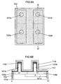
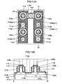
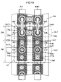
- FIG. 2 is a plane view of an SRAM in Embodiment 1 of the present invention.
- a unit cell UC shown in FIG. 2 is repeatedly arranged in an SRAM cell array.
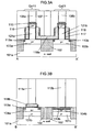
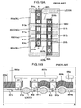
- FIGS. 3A to 3D show cross-sectional structures at the section lines A-A', B-B', C-C', and D-D' in the layout of FIG. 2 .
- An n- well or a first well 101a is formed on a substrate within an SRAM cell array. Diffusion layers on the substrate are separated by an element separator 102.
- a first memory node Qa1 formed by diffusion layers on the substrate is formed by a first p+ diffusion layer 103a and a first n+ diffusion layer 104a and is connected by a first silicide layer 113a formed on the substrate surface.
- a second memory node Qb1 formed by diffusion layers on the substrate is formed by a second p+ diffusion layer 103b and a second n+ diffusion layer 104b and is connected by a second silicide layer 113b formed on the substrate surface.
- a first anti-leak diffusion layer 101b or second anti-leak diffusion layer 101c consisting of a p+ diffusion layer is formed between the first well 101a and first n+ diffusion layer 104a.
- the first anti-leak diffusion layer 101b and second anti-leak diffusion layer 101c are each separated by the element separator 102 in each diffusion layer on the substrate.
- Qp11 and Qp21 are PMOS access transistors for accessing the memory cell.
- Qn11 and Qn21 are NMOS driver transistors for driving the memory cell.
- one unit cell UC comprises transistors arranged in two rows and two columns on the substrate. Arranged in the first column, the access transistor Qp11 and driver transistor Qn11 are provided on the first memory node Qa1 in this order from the top in the figure. Arranged in the second column, the access transistor Qp21 and driver transistor Qn21 are provided on the second memory node Qb in this order from the top in the figure.
- the SRAM cell array of this embodiment is constructed by successively arranging the unit cells UC having such four transistors in the vertical direction in the figure.
- a contact 110a formed on the first memory node Qa1 is connected to a contact 111b formed on a gate wire extending from the gate electrode of the driver transistor Qn21 by a node connection wire Na1 .
- a contact 110b formed on the second memory node Qb1 is connected to a contact 111a formed on a gate wire extending from the gate electrode of the driver transistor Qn11 by a node connection wire Nb1 .
- a contact 106a formed in the upper part of the access transistor Qp11 is connected to the bit line BL1 .
- a contact 106b formed in the upper part of the access transistor Qp21 is connected to the bit line BLB1 .
- a common contact 107 formed on a gate wire extending from the gate electrodes of the access transistor Qp11 and access transistor Qp21 is connected to the word line WL1 .
- the gate wire extending from the gate electrode of an access transistor Qp11 or Qp21 is shared with an adjoining cell in the crosswise direction and a contact on the gate wire is formed between the adjoining cells.
- Contacts ( 108a , 108b) formed in the upper parts of the driver transistors ( Qn11 , Qn21) are connected to the ground potential wiring layer Vss1 . It is desirable that the word line, bit lines, and ground potential wire are connected in a layer above the node connection wires or intra-memory cell wires so as to be shared with the other memory cells.
- the node connection wire (Na1), node connection wire ( Nb1 ), and ground potential wire ( Vss1 ) are provided in a layer below the bit lines ( BL1 , BLB1 ) and the word line ( WL1 ) is provided in a layer above the bit lines ( BL1 , BLB1 ) so that undesired contact between the wires and contacts does not occur.
- FIG. 2 shows an n+ injection region 125 and a p+ injection region 124.
- the pattern for forming the n+ injection region 125 and p+ injection region 124 consists of simple lines and spaces. Therefore, there is very little influence of dimensional variations and misalignment. The dimensional margin around the boundary between the n+ and p+ injection regions 124 and 125 is minimized. In the figure, the vertical length of the SRAM cell (the length in the connection direction of SRAM cells) is effectively reduced.
- the memory nodes Qa1 and Qb1 and gate wires shown in the layout of FIG. 2 are all rectangular in shape. Therefore, the pattern can easily be corrected in shape by OPC (optical proximity correction), which is suitable for attaining a small SRAM cell area.
- OPC optical proximity correction
- the source and drain of each transistor composing the SRAM are defined as follows.
- a diffusion layer formed in the upper part of a columnar semiconductor layer connected to a ground voltage is defined as the source diffusion layer and a diffusion layer formed in the lower part of the columnar semiconductor layer is defmed as the drain diffusion layer.
- diffusion layers formed in the upper and lower parts of a columnar semiconductor layer serve either as a source or as a drain depending on the operation state.
- the diffusion layer formed in the upper part of a columnar semiconductor layer is defined as the source diffusion layer and the diffusion layer formed in the lower part of the columnar semiconductor layer is defined as the drain diffusion layer for convenience.
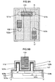
- FIG. 3A an n- well or a first well 101a shared in an SRAM cell array is formed in a substrate and diffusion layers on the substrate are separated by an element separator 102.
- a first p+ drain diffusion layer 103a is formed for the first memory node Qa1 formed by diffusion layers on the substrate by impurity implantation.
- a second p+ drain diffusion layer 103b is formed for the second memory node Qb1 formed by diffusion layers on the substrate by impurity implantation.
- first and second silicide layers are formed on the first and second p+ drain diffusion layers ( 103a , 103b), respectively.
- a columnar silicon layer 121a composing the access transistor Qp11 is formed on the first p+ drain diffusion layer 103a and a columnar silicon layer 121b composing the access transistor Qp21 is formed on the second p+ drain diffusion layer 103b.
- a gate insulating film 117 and a gate electrode 118 are formed around each columnar silicon layer.
- a p+ source diffusion layer 116 is formed in the upper part of the columnar silicon layer by impurity implantation and a silicide layer 115 is formed on the surface of the source diffusion layer.
- a contact 106a formed on the access transistor Qp11 is connected to the bit line BL1 and a contact 106b formed on the access transistor Qp21 is connected to the bit line BLB1 .
- a contact 107 formed on a gate wire 118a extending from the gates of the access transistors Qp11 and Qp21 is connected to the word line WL1 .
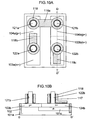
- the n- well or the first well 101a shared in the SRAM cell array is formed in the substrate and the diffusion layers on the substrate are separated by the element separator 102.
- a first n+ drain diffusion layer 104a is formed for the first memory node Qa1 formed by diffusion layers on the substrate by impurity implantation and a second n+ drain diffusion layer 104b is formed for the second memory node Qb1 formed by diffusion layers on the substrate by impurity implantation.
- the first and second silicide layers ( 113a , 113b) are formed on the first and second n+ drain diffusion layers ( 104a , 104b), respectively.
- a contact 111a formed on the first n+ drain diffusion layer 104a is formed on around the boundary area between the first p+ drain diffusion layer 103a and first n+ drain diffusion layer 104a and connected to a contact 111a formed on a gate wire 118b extending from the gate electrode of the driver transistor Qn11 via a memory node connection wire Na1 .
- a first anti-leak diffusion layer 101b consisting of a p+ diffusion layer is formed between the first well 101a and first n+ drain diffusion layer 104a .
- a second anti-leak diffusion layer 101c consisting of a p+ diffusion layer is formed between the first well 101a and second n+ drain diffusion layer 104b.
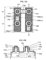
- the n- well or the first well 101a shared in the SRAM cell array is formed in the substrate and the diffusion layers on the substrate are separated by the element separator 102.
- the first n+ drain diffusion layer 104a is formed for the first node Qa1 formed by diffusion layers on the substrate by impurity implantation and the second n+ drain diffusion layer 104b is formed for the second memory node Qb1 formed by diffusion layers on the substrate by impurity implantation.
- the first and second silicide layers (113a, 113b) are formed on the surfaces of the first and second n+ drain diffusion layers ( 104a , 104b), respectively.
- the first anti-leak diffusion layer 101b consisting of a p+ diffusion layer is formed between the first well 101a and first n+ drain diffusion layer 104a . Furthermore, in order to prevent leak from the second n+ drain diffusion layer 104b having the same conductivity type as the first well 101a to the substrate, the second anti-leak diffusion layer 101c consisting of a p+ diffusion layer is formed between the first well 101a and second n+ diffusion layer 104b.
- a columnar silicon layer 122a forming the driver transistor Qn11 is formed on the first n+ drain diffusion layer 104a and a columnar silicon layer 122b forming the driver transistor Qn21 is formed on the second n+ drain diffusion layer 104b.
- a gate insulating film 117 and a gate electrode 118 are formed around each columnar silicon layer.
- An n+ source diffusion layer 114 is formed in the upper part of the columnar silicon layer by impurity implantation and a silicide layer 115 is formed on the surface of the source diffusion layer. Both contacts (108a, 108b) formed on the driver transistors (Qn11, Qn21) are connected to the ground potential Vss1 via a wiring layer.
- the n- well or the first well 101a shared in the SRAM cell array is formed in the substrate and the diffusion layers on the substrate are separated by the element separator 102.
- a second p+ drain diffusion layer 103b and a second n+ drain diffusion layer 104b are formed for the second memory node Qb formed by diffusion layers on the substrate by impurity implantation.
- a second silicide layer 113b is formed on the drain diffusion layer. The second p+ drain diffusion layer 103b and second n+ drain diffusion layer 104b are directly connected by the second silicide layer 113b.
- the second anti-leak diffusion layer 101c consisting of a p+ diffusion layer is formed between the first well 101a and second n+ drain diffusion layer 104b.
- a columnar silicon layer 122b composing the access transistor Qp21 is formed on the second p+ drain diffusion layer 103b and a columnar silicon layer 122b composing the driver transistor Qn21 is formed on the second n+ drain diffusion layer 104b.
- a gate insulating film 117 and a gate electrode 118 are formed around each of the p and n columnar silicon layers.
- a source diffusion layer is formed in the upper part of each columnar silicon layer by impurity implantation.
- a silicide layer 115 is formed on the surface of the source diffusion layer.
- a contact 108b formed on the access transistor Qp21 is connected to the bit line BLB1 and a contact 108b formed on the driver transistor Qn21 is connected to the ground potential Vss1 .
- a contact 110b is formed on a gate wire 118c extending from the gate electrode of the driver transistor Qn21 .
- the contact 110b is connected to a contact 111a formed on the first n+ drain diffusion layer 104a via a memory node connection wire Na1 .
- a contact 111b is formed on the second n+ drain diffusion layer 104b.
- the contact 111b is connected to a contact 111a formed on a gate wire 118b extending from the gate electrode of the driver transistor Qn11 via a memory node connection wire Nb1 .
- the n+ drain diffusion layer and p+ drain diffusion layer forming the memory nodes ( Qa1 , Qb1 ) are directly connected by a silicide layer, whereby the access transistor and driver transistor share a drain diffusion layer and function as a memory node of an SRAM. Therefore, there is no need of forming an element separator separating the n+ drain diffusion layer from the p+ drain diffusion layer. Only the element separator separating two memory nodes of an SRAM is necessary, attaining a small SRAM cell area.
- an SRAM cell having a structure in which a first well 201a is a p- well and a first and second anti-leak diffusion layers 201b and 201c consisting of n+ diffusion layers are formed between an n+ diffusion layer and the substrate can similarly be formed.
- the first anti-leak diffusion layer 201b is formed between a p+ drain diffusion layer 203a and the first well 201a
- the second anti-leak diffusion layer 201c is formed between a p+ drain diffusion layer 203b and the first well 201a so as to prevent leak from the diffusion layer to the substrate.
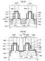
- FIGS. 5A to 13B An example of a method of producing the semiconductor memory device of the present invention will be described hereafter with reference to FIGS. 5A to 13B .
- A is a plane view and B is a cross-sectional view at a line D-D' in A.
- a silicon nitride film or the like is formed on a substrate, a pattern for columnar silicon layers (121a, 122a , 121b, 122b) is formed by lithography, and etching is performed to form a silicon nitride film mask 119 and columnar silicon layers (121a, 122a , 121b , 122b). Subsequently, an n- well or a first well 101a is formed in an SRAM cell array by impurity implantation.
- an element separator 102 is formed.
- the element separator is formed by first etching a groove pattern, filling the groove pattern with an oxide film by CVD or the like, and removing any extra oxide film on the substrate by dry or wet etching. Consequently, a diffusion layer pattern composing a first memory node Qa1 and a second memory node Qb1 is formed on the substrate.
- impurities are introduced in a p+ injection region 124 and an n+ injection region 125, respectively, by ion implantation to form drain diffusion layers ( 103a , 103b, 104a , 104b) in the lower parts of the columnar silicon layers on the substrate.
- drain diffusion layers 103a , 103b, 104a , 104b
- a second anti-leak diffusion layer 101c or a p+ diffusion layer is formed.
- the second anti-leak diffusion layer 101c can be formed by impurity implantation using a mask for the n+ injection region 125.
- a gate insulating film 117 and a gate conductive film 118 are formed.
- the gate insulating film 117 is formed by an oxide film or High-k film.
- the gate conductive film 118 is formed by a polysilicon or metal film.
- a gate wire pattern is formed by lithography using a resist 133.
- the gate conductive film 117 and gate insulating film 118 are etched using the resist 133 as a mask and the resist 133 is removed. Then, gate wires (118a to 118c) are formed. Then, a mask 119 on the pillars is removed.
- an insulating film such as a silicon nitride film is formed and etched back so that an insulating film 134 such as a silicon nitride film covers the sidewalls of columnar silicon layers and the sidewalls of gate electrodes.
- impurities are introduced in the p+ injection region 124 and n+ injection region 125, respectively, by ion implantation to form source diffusion layers (114, 116) in the upper parts of the columnar silicon layers.
- silicide layers (113a, 113b) on the drain diffusion layers and a silicide layer 115 on the source diffusion layers in the upper parts of the columnar silicon layers are formed by sputtering of a metal such as Ni and heat treatment.
- the insulating film 134 such as a silicon nitride film covering the sidewalls of the columnar silicon layers and gate electrodes prevents any drain-gate or source-gate shortcircuit which may occur due to the silicide layer.
- contacts (106a to 111a, 106b to 111b) are formed after a silicon oxide film or an interlayer film is formed.
- the SRAM cell of the present invention has limitation on layout at many points because of the minimum distance between contacts. Therefore, the contacts on the columnar silicon layers are formed in the first lithography and etching and the contacts on the diffusion layers and gates are formed in the second lithography and etching. In this way, the minimum distance between the contacts on the columnar silicon layers and the contacts on the diffusion layers and gates can be reduced, whereby further reducing the SRAM cell area.
- the contacts on the gates can be formed in the same step as the contacts on the columnar silicon layers.
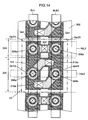
- FIG. 14 is a plane view of the SRAM of Embodiment 2 of the present invention. This embodiment is different from Embodiment 1 in the following point.
- the memory node Qa3 formed by the first diffusion layer on the substrate and the gate wire extending from the gate electrode of the driver transistor Qn23 are connected by a common contact 310a extending over them.
- the memory node Qb3 formed by the second diffusion layer on the substrate and the gate wire extending from the gate electrode of the driver transistor Qn13 are connected by a common contact 310b extending over them.
- the gate and memory node are connected by a contact, not by a wiring layer, as described above; the number of contacts in an SRAM cell can be reduced.
- the cell area can be reduced by adjusting the positions of columnar silicon layers and contacts.
- the word line, bit lines, and ground potential wire are desirably provided in a layer above the node connection wires or intra-memory cell wires so as to be shared with the other memory cells.
- the node connection wires are formed by contacts. Except for this point, the same structure as in Embodiment 1 is employed and further explanation is omitted.
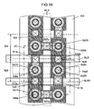
- FIG. 15 is a plane view of the SRAM of Embodiment 3 of the present invention.
- This embodiment is different from Embodiments 1 and 2 in the following point.
- the contact (110a, 210a ) adjoins only the driver transistor ( Qn11 , Qn12 ) on the memory node Qa while the contact (110b, 210b ) are provided on the diffusion layer between the driver transistor (Qn21, Qn22) and access transistor ( Qp21 , Qp22 ) on the memory node Qb.
- This asymmetric layout causes asymmetry in characteristics of the SRAM cell and may narrow the operational margin.
- a vertically (longitudinally) and horizontally (laterally) symmetric layout is employed. Therefore, deterioration in the operational margin due to the above asymmetry does not occur, attaining an SRAM cell having a broad operational margin.
- a memory node Qa4 formed by the first diffusion layer on the substrate and the gate wire extending from the gate electrode of a driver transistor Qn24 are connected by a common contact 410a extending over them.
- a memory node Qb4 formed by the second diffusion layer on the substrate and the gate wire extending from the gate electrode of a driver transistor Qn14 are connected by a common contact 410b extending over them.
- the word line, bit lines, and ground potential wire are desirably provided in a layer above the node connection wires or intra-memory cell wires so as to be shared with the other memory cells.
- the node connection wires are formed by contacts.
- a ground potential wire Vss4 and a word line WL4 are provided in the same layer and bit lines (BL4, BLB4) are provided in a layer above the word line WL4 so that undesired contact between the wires and contacts does not occur.
- FIG. 16 is a plane view of the SRAM of Embodiment 4 of the present invention.
- a vertically (longitudinally) and horizontally (laterally) symmetric layout is used as in Embodiment 3 and, therefore, the above problems due to asymmetry do not occur. Then, an SRAM cell having a broader operational margin can be attained.
- the word line, bit lines, and ground potential wire are desirably provided in a layer above the node connection wires or intra-memory cell wires so as to be shared with the other memory cells.
- a node connection wire (Na5), node connection wire (Nb5), and ground potential wire ( Vss5 ) are provided in a lower layer than a word line ( WL5 ), and bit lines (BL5, BLB5) are provided in an upper layer than the word line ( WL5 ) so that undesired contact between the wires and contacts does not occur.
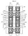
- FIG. 17 is a plane view of the SRAM of Embodiment 5 of the present invention.
- This embodiment is different from Embodiment 1 in that the columnar silicon layers forming access transistors are different in shape and the columnar silicon layers forming driver transistor are different in size.
- the leak current of access transistors should be larger than the leak current of driver transistors.
- the leak current of access transistors can be increased by enlarging the columnar silicon layers forming access transistors as shown in FIG. 17 .
- the columnar silicon layers of driver transistors are enlarged so as to increase the current of the driver transistors, whereby the reading margin can be improved
- Embodiment 1 the same layout as in Embodiment 1 is employed by way of example. In practice, it is not restricted to the layout of Embodiment 1 and this embodiment can similarly apply to the layouts of the other embodiments.
- the word line, bit lines, power supply potential wire, and ground potential wire are desirably provided in a layer above the node connection wires or intra-memory cell wires so as to be shared with the other memory cells.
- the same hierarchical wire configuration as in Embodiment 1 can be attained. Except for this point, the same structure as in Embodiment 1 is employed and further explanation is omitted.
- FIG. 18 is a plane view of the SRAM of Embodiment 6 of the present invention. This embodiment is different from Embodiment 1 in the flowing point.
- the cells, at immediately upper and lower positions in the plane of the sheet face of the figure, of the SRAM cell shown as the unit cell UC are inverted from Embodiment 1.
- Contacts ( 706a, 706b ) formed on access transistors ( Qb17, Qb27 ) and connected to bit lines are common contacts also used as the contacts of the SRAM cell, at immediately upper positions in the plane of the sheet face of the figure, that are connected to the bit lines.
- this SRAM cell has the same layout as of Embodiment 1.
- Embodiment 1 the same layout as in Embodiment 1 is employed by way of example. In practice, it is not restricted to the layout of Embodiment 1 and this embodiment can similarly apply to the layouts of the other embodiments.
- the word line, bit lines, power supply potential wire, and ground potential wire are desirably provided in a layer above the node connection wires or intra-memory cell wires so as to be shared with the other memory cells.
- the same hierarchical wire configuration as in Embodiment 1 can be attained. Except for this point, the same structure as in Embodiment 1 is employed and further explanation is omitted.
Landscapes
- Semiconductor Memories (AREA)
- Static Random-Access Memory (AREA)
Applications Claiming Priority (1)
| Application Number | Priority Date | Filing Date | Title |
|---|---|---|---|
| JP2009211300A JP5524547B2 (ja) | 2009-09-14 | 2009-09-14 | 半導体記憶装置 |
Publications (2)
| Publication Number | Publication Date |
|---|---|
| EP2296176A1 EP2296176A1 (en) | 2011-03-16 |
| EP2296176B1 true EP2296176B1 (en) | 2014-08-20 |
Family
ID=43034204
Family Applications (1)
| Application Number | Title | Priority Date | Filing Date |
|---|---|---|---|
| EP10009572.8A Active EP2296176B1 (en) | 2009-09-14 | 2010-09-14 | SRAM cell with four SGTs and manufacturing method thereof |
Country Status (6)
| Country | Link |
|---|---|
| US (1) | US8169030B2 (enExample) |
| EP (1) | EP2296176B1 (enExample) |
| JP (1) | JP5524547B2 (enExample) |
| KR (1) | KR101160105B1 (enExample) |
| CN (1) | CN102024815B (enExample) |
| TW (1) | TW201110327A (enExample) |
Families Citing this family (24)
| Publication number | Priority date | Publication date | Assignee | Title |
|---|---|---|---|---|
| JP2013016243A (ja) * | 2011-06-09 | 2013-01-24 | Semiconductor Energy Lab Co Ltd | 記憶装置 |
| WO2013121536A1 (ja) * | 2012-02-15 | 2013-08-22 | ユニサンティス エレクトロニクス シンガポール プライベート リミテッド | 半導体記憶装置 |
| WO2013121537A1 (ja) * | 2012-02-15 | 2013-08-22 | ユニサンティス エレクトロニクス シンガポール プライベート リミテッド | 半導体記憶装置 |
| US8755219B2 (en) | 2012-02-15 | 2014-06-17 | Unisantis Electronics Singapore Pte. Ltd. | Hierarchical wordline loadless 4GST-SRAM with a small cell area |
| US8836051B2 (en) * | 2012-06-08 | 2014-09-16 | Unisantis Electronics Singapore Pte. Ltd. | Method for producing semiconductor device and semiconductor device |
| KR101925012B1 (ko) * | 2012-07-17 | 2018-12-05 | 에스케이하이닉스 주식회사 | 반도체 장치 및 그의 제조 방법 |
| US9082838B2 (en) * | 2012-09-28 | 2015-07-14 | Unisantis Electronics Singapore Pte. Ltd. | Method for producing a semiconductor device and semiconductor device |
| US8969949B2 (en) * | 2013-03-10 | 2015-03-03 | Taiwan Semiconductor Manufacturing Company, Ltd. | Structure and method for static random access memory device of vertical tunneling field effect transistor |
| JP5740535B1 (ja) * | 2013-07-19 | 2015-06-24 | ユニサンティス エレクトロニクス シンガポール プライベート リミテッドUnisantis Electronics Singapore Pte Ltd. | 半導体装置の製造方法、及び、半導体装置 |
| JP2015032651A (ja) * | 2013-08-01 | 2015-02-16 | マイクロン テクノロジー, インク. | 半導体装置 |
| WO2015019444A1 (ja) * | 2013-08-07 | 2015-02-12 | ユニサンティス エレクトロニクス シンガポール プライベート リミテッド | 半導体装置の製造方法、及び、半導体装置 |
| US10361270B2 (en) * | 2013-11-20 | 2019-07-23 | Taiwan Semiconductor Manufacturing Co., Ltd. | Nanowire MOSFET with different silicides on source and drain |
| JP5832057B1 (ja) * | 2014-02-24 | 2015-12-16 | ユニサンティス エレクトロニクス シンガポール プライベート リミテッドUnisantis Electronics Singapore Pte Ltd. | 記憶装置、半導体装置、及び記憶装置、半導体装置の製造方法 |
| WO2015129021A1 (ja) * | 2014-02-28 | 2015-09-03 | ユニサンティス エレクトロニクス シンガポール プライベート リミテッド | 半導体装置、及び半導体装置の製造方法 |
| JP6114425B2 (ja) * | 2016-03-11 | 2017-04-12 | ユニサンティス エレクトロニクス シンガポール プライベート リミテッドUnisantis Electronics Singapore Pte Ltd. | 半導体装置の製造方法、及び、半導体装置 |
| CN109196584B (zh) * | 2016-08-31 | 2022-07-19 | 美光科技公司 | 感测放大器构造 |
| EP3840046B1 (en) | 2016-08-31 | 2025-03-19 | Micron Technology, Inc. | Memory cells and memory arrays |
| CN110192280A (zh) | 2017-01-12 | 2019-08-30 | 美光科技公司 | 存储器单元、双晶体管单电容器存储器单元阵列、形成双晶体管单电容器存储器单元阵列的方法及用于制造集成电路的方法 |
| US10290639B2 (en) * | 2017-09-12 | 2019-05-14 | Globalfoundries Inc. | VNW SRAM with trinity cross-couple PD/PU contact and method for producing the same |
| US10559572B2 (en) | 2018-06-29 | 2020-02-11 | International Business Machines Corporation | Vertical transistor contact for a memory cell with increased density |
| US10566453B2 (en) | 2018-06-29 | 2020-02-18 | International Business Machines Corporation | Vertical transistor contact for cross-coupling in a memory cell |
| CN109326650B (zh) * | 2018-10-10 | 2022-04-19 | 中国科学院微电子研究所 | 半导体器件及其制造方法及包括该器件的电子设备 |
| US11640987B2 (en) * | 2021-02-04 | 2023-05-02 | Applied Materials, Inc. | Implant to form vertical FETs with self-aligned drain spacer and junction |
| WO2022239196A1 (ja) * | 2021-05-13 | 2022-11-17 | ユニサンティス エレクトロニクス シンガポール プライベート リミテッド | 半導体素子を用いたメモリ装置 |
Family Cites Families (16)
| Publication number | Priority date | Publication date | Assignee | Title |
|---|---|---|---|---|
| JPS60128654A (ja) * | 1983-12-16 | 1985-07-09 | Hitachi Ltd | 半導体集積回路 |
| JPS63239973A (ja) * | 1986-10-08 | 1988-10-05 | テキサス インスツルメンツ インコーポレイテツド | 集積回路およびその製造方法 |
| JP2703970B2 (ja) | 1989-01-17 | 1998-01-26 | 株式会社東芝 | Mos型半導体装置 |
| KR0121992B1 (ko) | 1993-03-03 | 1997-11-12 | 모리시다 요이치 | 반도체장치 및 그 제조방법 |
| JP3403231B2 (ja) * | 1993-05-12 | 2003-05-06 | 三菱電機株式会社 | 半導体装置およびその製造方法 |
| JP3036588B2 (ja) * | 1997-02-03 | 2000-04-24 | 日本電気株式会社 | 半導体記憶装置 |
| JP3467416B2 (ja) | 1998-04-20 | 2003-11-17 | Necエレクトロニクス株式会社 | 半導体記憶装置及びその製造方法 |
| US6229161B1 (en) * | 1998-06-05 | 2001-05-08 | Stanford University | Semiconductor capacitively-coupled NDR device and its applications in high-density high-speed memories and in power switches |
| KR20010062611A (ko) * | 1999-12-23 | 2001-07-07 | 윌리엄 비. 켐플러 | 동적 임계 전압 4t sram 셀 |
| US6583452B1 (en) * | 2001-12-17 | 2003-06-24 | T-Ram, Inc. | Thyristor-based device having extended capacitive coupling |
| WO2003082954A1 (en) * | 2002-03-28 | 2003-10-09 | Communications Research Laboratory, Independent Administrative Institution | Process for production of molecular devices |
| US7138685B2 (en) | 2002-12-11 | 2006-11-21 | International Business Machines Corporation | Vertical MOSFET SRAM cell |
| JP2005303111A (ja) * | 2004-04-14 | 2005-10-27 | Renesas Technology Corp | 半導体記憶装置 |
| JP5114968B2 (ja) * | 2007-02-20 | 2013-01-09 | 富士通セミコンダクター株式会社 | 半導体装置及びその製造方法 |
| WO2009095999A1 (ja) * | 2008-01-29 | 2009-08-06 | Unisantis Electronics (Japan) Ltd. | 半導体記憶装置 |
| US8288795B2 (en) * | 2010-03-02 | 2012-10-16 | Micron Technology, Inc. | Thyristor based memory cells, devices and systems including the same and methods for forming the same |
-
2009
- 2009-09-14 JP JP2009211300A patent/JP5524547B2/ja not_active Expired - Fee Related
-
2010
- 2010-09-13 TW TW099130837A patent/TW201110327A/zh unknown
- 2010-09-14 US US12/881,554 patent/US8169030B2/en active Active
- 2010-09-14 CN CN2010102843051A patent/CN102024815B/zh active Active
- 2010-09-14 KR KR1020100089932A patent/KR101160105B1/ko active Active
- 2010-09-14 EP EP10009572.8A patent/EP2296176B1/en active Active
Also Published As
| Publication number | Publication date |
|---|---|
| KR20110029101A (ko) | 2011-03-22 |
| EP2296176A1 (en) | 2011-03-16 |
| CN102024815B (zh) | 2013-04-10 |
| US8169030B2 (en) | 2012-05-01 |
| US20110062523A1 (en) | 2011-03-17 |
| JP2011061110A (ja) | 2011-03-24 |
| KR101160105B1 (ko) | 2012-06-26 |
| CN102024815A (zh) | 2011-04-20 |
| TW201110327A (en) | 2011-03-16 |
| JP5524547B2 (ja) | 2014-06-18 |
Similar Documents
| Publication | Publication Date | Title |
|---|---|---|
| EP2296176B1 (en) | SRAM cell with four SGTs and manufacturing method thereof | |
| EP2254149B1 (en) | SRAM using vertical transistors with a diffusion layer for reducing leakage currents | |
| JP4756221B2 (ja) | 半導体記憶装置 | |
| KR101182025B1 (ko) | 반도체 기억장치 | |
| CN101933136B (zh) | 半导体存储器件 | |
| US8507995B2 (en) | Semiconductor memory device | |
| SG177041A1 (en) | Rom cell circuit for finfet devices | |
| US10153264B2 (en) | Static random access memory (SRAM) cell including fin-type transistor | |
| KR20130116334A (ko) | 반도체 기억 장치 | |
| KR20130118949A (ko) | 반도체 기억 장치 | |
| JP5489272B2 (ja) | 半導体記憶装置 | |
| JPWO2013121537A1 (ja) | 半導体記憶装置 | |
| KR20070023458A (ko) | 풀 씨모스형 에스램 셀 | |
| JPWO2013121536A1 (ja) | 半導体記憶装置 |
Legal Events
| Date | Code | Title | Description |
|---|---|---|---|
| PUAI | Public reference made under article 153(3) epc to a published international application that has entered the european phase |
Free format text: ORIGINAL CODE: 0009012 |
|
| AK | Designated contracting states |
Kind code of ref document: A1 Designated state(s): AL AT BE BG CH CY CZ DE DK EE ES FI FR GB GR HR HU IE IS IT LI LT LU LV MC MK MT NL NO PL PT RO SE SI SK SM TR |
|
| AX | Request for extension of the european patent |
Extension state: BA ME RS |
|
| 17P | Request for examination filed |
Effective date: 20110315 |
|
| 17Q | First examination report despatched |
Effective date: 20110728 |
|
| RAP1 | Party data changed (applicant data changed or rights of an application transferred) |
Owner name: UNISANTIS ELECTRONICS SINGAPORE PTE. LTD. |
|
| RAP1 | Party data changed (applicant data changed or rights of an application transferred) |
Owner name: UNISANTIS ELECTRONICS SINGAPORE PTE. LTD. |
|
| RIC1 | Information provided on ipc code assigned before grant |
Ipc: H01L 27/02 20060101ALI20140328BHEP Ipc: H01L 21/8244 20060101AFI20140328BHEP Ipc: H01L 27/11 20060101ALI20140328BHEP Ipc: H01L 21/8238 20060101ALI20140328BHEP Ipc: H01L 29/10 20060101ALI20140328BHEP |
|
| GRAP | Despatch of communication of intention to grant a patent |
Free format text: ORIGINAL CODE: EPIDOSNIGR1 |
|
| INTG | Intention to grant announced |
Effective date: 20140602 |
|
| GRAS | Grant fee paid |
Free format text: ORIGINAL CODE: EPIDOSNIGR3 |
|
| GRAA | (expected) grant |
Free format text: ORIGINAL CODE: 0009210 |
|
| AK | Designated contracting states |
Kind code of ref document: B1 Designated state(s): AL AT BE BG CH CY CZ DE DK EE ES FI FR GB GR HR HU IE IS IT LI LT LU LV MC MK MT NL NO PL PT RO SE SI SK SM TR |
|
| REG | Reference to a national code |
Ref country code: GB Ref legal event code: FG4D |
|
| RIN1 | Information on inventor provided before grant (corrected) |
Inventor name: ARAI, SHINTARO Inventor name: MASUOKA, FUJIO |
|
| REG | Reference to a national code |
Ref country code: CH Ref legal event code: EP |
|
| REG | Reference to a national code |
Ref country code: AT Ref legal event code: REF Ref document number: 683859 Country of ref document: AT Kind code of ref document: T Effective date: 20140915 |
|
| REG | Reference to a national code |
Ref country code: IE Ref legal event code: FG4D |
|
| REG | Reference to a national code |
Ref country code: DE Ref legal event code: R096 Ref document number: 602010018329 Country of ref document: DE Effective date: 20141002 |
|
| REG | Reference to a national code |
Ref country code: AT Ref legal event code: MK05 Ref document number: 683859 Country of ref document: AT Kind code of ref document: T Effective date: 20140820 |
|
| REG | Reference to a national code |
Ref country code: NL Ref legal event code: VDEP Effective date: 20140820 |
|
| REG | Reference to a national code |
Ref country code: LT Ref legal event code: MG4D |
|
| PG25 | Lapsed in a contracting state [announced via postgrant information from national office to epo] |
Ref country code: LT Free format text: LAPSE BECAUSE OF FAILURE TO SUBMIT A TRANSLATION OF THE DESCRIPTION OR TO PAY THE FEE WITHIN THE PRESCRIBED TIME-LIMIT Effective date: 20140820 Ref country code: ES Free format text: LAPSE BECAUSE OF FAILURE TO SUBMIT A TRANSLATION OF THE DESCRIPTION OR TO PAY THE FEE WITHIN THE PRESCRIBED TIME-LIMIT Effective date: 20140820 Ref country code: NO Free format text: LAPSE BECAUSE OF FAILURE TO SUBMIT A TRANSLATION OF THE DESCRIPTION OR TO PAY THE FEE WITHIN THE PRESCRIBED TIME-LIMIT Effective date: 20141120 Ref country code: GR Free format text: LAPSE BECAUSE OF FAILURE TO SUBMIT A TRANSLATION OF THE DESCRIPTION OR TO PAY THE FEE WITHIN THE PRESCRIBED TIME-LIMIT Effective date: 20141121 Ref country code: FI Free format text: LAPSE BECAUSE OF FAILURE TO SUBMIT A TRANSLATION OF THE DESCRIPTION OR TO PAY THE FEE WITHIN THE PRESCRIBED TIME-LIMIT Effective date: 20140820 Ref country code: SE Free format text: LAPSE BECAUSE OF FAILURE TO SUBMIT A TRANSLATION OF THE DESCRIPTION OR TO PAY THE FEE WITHIN THE PRESCRIBED TIME-LIMIT Effective date: 20140820 Ref country code: PT Free format text: LAPSE BECAUSE OF FAILURE TO SUBMIT A TRANSLATION OF THE DESCRIPTION OR TO PAY THE FEE WITHIN THE PRESCRIBED TIME-LIMIT Effective date: 20141222 Ref country code: BG Free format text: LAPSE BECAUSE OF FAILURE TO SUBMIT A TRANSLATION OF THE DESCRIPTION OR TO PAY THE FEE WITHIN THE PRESCRIBED TIME-LIMIT Effective date: 20141120 |
|
| PG25 | Lapsed in a contracting state [announced via postgrant information from national office to epo] |
Ref country code: IS Free format text: LAPSE BECAUSE OF FAILURE TO SUBMIT A TRANSLATION OF THE DESCRIPTION OR TO PAY THE FEE WITHIN THE PRESCRIBED TIME-LIMIT Effective date: 20141220 Ref country code: LV Free format text: LAPSE BECAUSE OF FAILURE TO SUBMIT A TRANSLATION OF THE DESCRIPTION OR TO PAY THE FEE WITHIN THE PRESCRIBED TIME-LIMIT Effective date: 20140820 Ref country code: HR Free format text: LAPSE BECAUSE OF FAILURE TO SUBMIT A TRANSLATION OF THE DESCRIPTION OR TO PAY THE FEE WITHIN THE PRESCRIBED TIME-LIMIT Effective date: 20140820 Ref country code: AT Free format text: LAPSE BECAUSE OF FAILURE TO SUBMIT A TRANSLATION OF THE DESCRIPTION OR TO PAY THE FEE WITHIN THE PRESCRIBED TIME-LIMIT Effective date: 20140820 |
|
| PG25 | Lapsed in a contracting state [announced via postgrant information from national office to epo] |
Ref country code: NL Free format text: LAPSE BECAUSE OF FAILURE TO SUBMIT A TRANSLATION OF THE DESCRIPTION OR TO PAY THE FEE WITHIN THE PRESCRIBED TIME-LIMIT Effective date: 20140820 |
|
| PG25 | Lapsed in a contracting state [announced via postgrant information from national office to epo] |
Ref country code: EE Free format text: LAPSE BECAUSE OF FAILURE TO SUBMIT A TRANSLATION OF THE DESCRIPTION OR TO PAY THE FEE WITHIN THE PRESCRIBED TIME-LIMIT Effective date: 20140820 Ref country code: IT Free format text: LAPSE BECAUSE OF FAILURE TO SUBMIT A TRANSLATION OF THE DESCRIPTION OR TO PAY THE FEE WITHIN THE PRESCRIBED TIME-LIMIT Effective date: 20140820 Ref country code: DK Free format text: LAPSE BECAUSE OF FAILURE TO SUBMIT A TRANSLATION OF THE DESCRIPTION OR TO PAY THE FEE WITHIN THE PRESCRIBED TIME-LIMIT Effective date: 20140820 Ref country code: CZ Free format text: LAPSE BECAUSE OF FAILURE TO SUBMIT A TRANSLATION OF THE DESCRIPTION OR TO PAY THE FEE WITHIN THE PRESCRIBED TIME-LIMIT Effective date: 20140820 Ref country code: SK Free format text: LAPSE BECAUSE OF FAILURE TO SUBMIT A TRANSLATION OF THE DESCRIPTION OR TO PAY THE FEE WITHIN THE PRESCRIBED TIME-LIMIT Effective date: 20140820 Ref country code: RO Free format text: LAPSE BECAUSE OF FAILURE TO SUBMIT A TRANSLATION OF THE DESCRIPTION OR TO PAY THE FEE WITHIN THE PRESCRIBED TIME-LIMIT Effective date: 20140820 |
|
| REG | Reference to a national code |
Ref country code: CH Ref legal event code: PL |
|
| REG | Reference to a national code |
Ref country code: DE Ref legal event code: R097 Ref document number: 602010018329 Country of ref document: DE |
|
| PG25 | Lapsed in a contracting state [announced via postgrant information from national office to epo] |
Ref country code: PL Free format text: LAPSE BECAUSE OF FAILURE TO SUBMIT A TRANSLATION OF THE DESCRIPTION OR TO PAY THE FEE WITHIN THE PRESCRIBED TIME-LIMIT Effective date: 20140820 Ref country code: MC Free format text: LAPSE BECAUSE OF FAILURE TO SUBMIT A TRANSLATION OF THE DESCRIPTION OR TO PAY THE FEE WITHIN THE PRESCRIBED TIME-LIMIT Effective date: 20140820 |
|
| REG | Reference to a national code |
Ref country code: IE Ref legal event code: MM4A |
|
| PLBE | No opposition filed within time limit |
Free format text: ORIGINAL CODE: 0009261 |
|
| STAA | Information on the status of an ep patent application or granted ep patent |
Free format text: STATUS: NO OPPOSITION FILED WITHIN TIME LIMIT |
|
| PG25 | Lapsed in a contracting state [announced via postgrant information from national office to epo] |
Ref country code: BE Free format text: LAPSE BECAUSE OF NON-PAYMENT OF DUE FEES Effective date: 20140930 |
|
| 26N | No opposition filed |
Effective date: 20150521 |
|
| PG25 | Lapsed in a contracting state [announced via postgrant information from national office to epo] |
Ref country code: CH Free format text: LAPSE BECAUSE OF NON-PAYMENT OF DUE FEES Effective date: 20140930 Ref country code: LI Free format text: LAPSE BECAUSE OF NON-PAYMENT OF DUE FEES Effective date: 20140930 |
|
| PG25 | Lapsed in a contracting state [announced via postgrant information from national office to epo] |
Ref country code: IE Free format text: LAPSE BECAUSE OF NON-PAYMENT OF DUE FEES Effective date: 20140914 |
|
| PG25 | Lapsed in a contracting state [announced via postgrant information from national office to epo] |
Ref country code: SI Free format text: LAPSE BECAUSE OF FAILURE TO SUBMIT A TRANSLATION OF THE DESCRIPTION OR TO PAY THE FEE WITHIN THE PRESCRIBED TIME-LIMIT Effective date: 20140820 |
|
| PG25 | Lapsed in a contracting state [announced via postgrant information from national office to epo] |
Ref country code: SM Free format text: LAPSE BECAUSE OF FAILURE TO SUBMIT A TRANSLATION OF THE DESCRIPTION OR TO PAY THE FEE WITHIN THE PRESCRIBED TIME-LIMIT Effective date: 20140820 |
|
| PG25 | Lapsed in a contracting state [announced via postgrant information from national office to epo] |
Ref country code: CY Free format text: LAPSE BECAUSE OF FAILURE TO SUBMIT A TRANSLATION OF THE DESCRIPTION OR TO PAY THE FEE WITHIN THE PRESCRIBED TIME-LIMIT Effective date: 20140820 Ref country code: MT Free format text: LAPSE BECAUSE OF FAILURE TO SUBMIT A TRANSLATION OF THE DESCRIPTION OR TO PAY THE FEE WITHIN THE PRESCRIBED TIME-LIMIT Effective date: 20140820 |
|
| PG25 | Lapsed in a contracting state [announced via postgrant information from national office to epo] |
Ref country code: TR Free format text: LAPSE BECAUSE OF FAILURE TO SUBMIT A TRANSLATION OF THE DESCRIPTION OR TO PAY THE FEE WITHIN THE PRESCRIBED TIME-LIMIT Effective date: 20140820 Ref country code: BE Free format text: LAPSE BECAUSE OF FAILURE TO SUBMIT A TRANSLATION OF THE DESCRIPTION OR TO PAY THE FEE WITHIN THE PRESCRIBED TIME-LIMIT Effective date: 20140820 Ref country code: HU Free format text: LAPSE BECAUSE OF FAILURE TO SUBMIT A TRANSLATION OF THE DESCRIPTION OR TO PAY THE FEE WITHIN THE PRESCRIBED TIME-LIMIT; INVALID AB INITIO Effective date: 20100914 Ref country code: LU Free format text: LAPSE BECAUSE OF NON-PAYMENT OF DUE FEES Effective date: 20140914 |
|
| REG | Reference to a national code |
Ref country code: FR Ref legal event code: PLFP Year of fee payment: 7 |
|
| REG | Reference to a national code |
Ref country code: FR Ref legal event code: PLFP Year of fee payment: 8 |
|
| PG25 | Lapsed in a contracting state [announced via postgrant information from national office to epo] |
Ref country code: MK Free format text: LAPSE BECAUSE OF FAILURE TO SUBMIT A TRANSLATION OF THE DESCRIPTION OR TO PAY THE FEE WITHIN THE PRESCRIBED TIME-LIMIT Effective date: 20140820 |
|
| REG | Reference to a national code |
Ref country code: FR Ref legal event code: PLFP Year of fee payment: 9 |
|
| PG25 | Lapsed in a contracting state [announced via postgrant information from national office to epo] |
Ref country code: AL Free format text: LAPSE BECAUSE OF FAILURE TO SUBMIT A TRANSLATION OF THE DESCRIPTION OR TO PAY THE FEE WITHIN THE PRESCRIBED TIME-LIMIT Effective date: 20140820 |
|
| REG | Reference to a national code |
Ref country code: DE Ref legal event code: R079 Ref document number: 602010018329 Country of ref document: DE Free format text: PREVIOUS MAIN CLASS: H01L0021824400 Ipc: H10B0010000000 |
|
| PGFP | Annual fee paid to national office [announced via postgrant information from national office to epo] |
Ref country code: DE Payment date: 20250919 Year of fee payment: 16 |
|
| PGFP | Annual fee paid to national office [announced via postgrant information from national office to epo] |
Ref country code: GB Payment date: 20250918 Year of fee payment: 16 |
|
| PGFP | Annual fee paid to national office [announced via postgrant information from national office to epo] |
Ref country code: FR Payment date: 20250919 Year of fee payment: 16 |