EP2296176B1 - SRAM cell with four SGTs and manufacturing method thereof - Google Patents
SRAM cell with four SGTs and manufacturing method thereof Download PDFInfo
- Publication number
- EP2296176B1 EP2296176B1 EP10009572.8A EP10009572A EP2296176B1 EP 2296176 B1 EP2296176 B1 EP 2296176B1 EP 10009572 A EP10009572 A EP 10009572A EP 2296176 B1 EP2296176 B1 EP 2296176B1
- Authority
- EP
- European Patent Office
- Prior art keywords
- diffusion layer
- type diffusion
- leak
- type
- pmos access
- Prior art date
- Legal status (The legal status is an assumption and is not a legal conclusion. Google has not performed a legal analysis and makes no representation as to the accuracy of the status listed.)
- Active
Links
- 238000004519 manufacturing process Methods 0.000 title description 19
- 238000009792 diffusion process Methods 0.000 claims description 248
- 239000000758 substrate Substances 0.000 claims description 51
- 239000004065 semiconductor Substances 0.000 claims description 37
- 229910021332 silicide Inorganic materials 0.000 claims description 20
- FVBUAEGBCNSCDD-UHFFFAOYSA-N silicide(4-) Chemical compound [Si-4] FVBUAEGBCNSCDD-UHFFFAOYSA-N 0.000 claims description 20
- 238000005530 etching Methods 0.000 claims description 5
- 230000006870 function Effects 0.000 claims description 5
- 238000001459 lithography Methods 0.000 claims description 5
- 238000000034 method Methods 0.000 claims description 3
- 230000003068 static effect Effects 0.000 claims description 2
- 239000010410 layer Substances 0.000 description 204
- XUIMIQQOPSSXEZ-UHFFFAOYSA-N Silicon Chemical compound [Si] XUIMIQQOPSSXEZ-UHFFFAOYSA-N 0.000 description 36
- 229910052710 silicon Inorganic materials 0.000 description 36
- 239000010703 silicon Substances 0.000 description 36
- 239000012535 impurity Substances 0.000 description 14
- 238000002513 implantation Methods 0.000 description 12
- 238000002347 injection Methods 0.000 description 12
- 239000007924 injection Substances 0.000 description 12
- 229910052581 Si3N4 Inorganic materials 0.000 description 7
- HQVNEWCFYHHQES-UHFFFAOYSA-N silicon nitride Chemical compound N12[Si]34N5[Si]62N3[Si]51N64 HQVNEWCFYHHQES-UHFFFAOYSA-N 0.000 description 7
- VYPSYNLAJGMNEJ-UHFFFAOYSA-N Silicium dioxide Chemical compound O=[Si]=O VYPSYNLAJGMNEJ-UHFFFAOYSA-N 0.000 description 3
- 230000010354 integration Effects 0.000 description 3
- 229910052814 silicon oxide Inorganic materials 0.000 description 3
- 238000005468 ion implantation Methods 0.000 description 2
- 239000002184 metal Substances 0.000 description 2
- 230000006866 deterioration Effects 0.000 description 1
- 238000001312 dry etching Methods 0.000 description 1
- 238000005516 engineering process Methods 0.000 description 1
- 238000010438 heat treatment Methods 0.000 description 1
- 239000011229 interlayer Substances 0.000 description 1
- 230000003287 optical effect Effects 0.000 description 1
- 229910021420 polycrystalline silicon Inorganic materials 0.000 description 1
- 229920005591 polysilicon Polymers 0.000 description 1
- 238000004544 sputter deposition Methods 0.000 description 1
- 238000001039 wet etching Methods 0.000 description 1
Images


Classifications
-
- H—ELECTRICITY
- H01—ELECTRIC ELEMENTS
- H01L—SEMICONDUCTOR DEVICES NOT COVERED BY CLASS H10
- H01L27/00—Devices consisting of a plurality of semiconductor or other solid-state components formed in or on a common substrate
- H01L27/02—Devices consisting of a plurality of semiconductor or other solid-state components formed in or on a common substrate including semiconductor components specially adapted for rectifying, oscillating, amplifying or switching and having at least one potential-jump barrier or surface barrier; including integrated passive circuit elements with at least one potential-jump barrier or surface barrier
- H01L27/0203—Particular design considerations for integrated circuits
- H01L27/0207—Geometrical layout of the components, e.g. computer aided design; custom LSI, semi-custom LSI, standard cell technique
-
- H—ELECTRICITY
- H01—ELECTRIC ELEMENTS
- H01L—SEMICONDUCTOR DEVICES NOT COVERED BY CLASS H10
- H01L21/00—Processes or apparatus adapted for the manufacture or treatment of semiconductor or solid state devices or of parts thereof
- H01L21/70—Manufacture or treatment of devices consisting of a plurality of solid state components formed in or on a common substrate or of parts thereof; Manufacture of integrated circuit devices or of parts thereof
- H01L21/77—Manufacture or treatment of devices consisting of a plurality of solid state components or integrated circuits formed in, or on, a common substrate
- H01L21/78—Manufacture or treatment of devices consisting of a plurality of solid state components or integrated circuits formed in, or on, a common substrate with subsequent division of the substrate into plural individual devices
- H01L21/82—Manufacture or treatment of devices consisting of a plurality of solid state components or integrated circuits formed in, or on, a common substrate with subsequent division of the substrate into plural individual devices to produce devices, e.g. integrated circuits, each consisting of a plurality of components
- H01L21/822—Manufacture or treatment of devices consisting of a plurality of solid state components or integrated circuits formed in, or on, a common substrate with subsequent division of the substrate into plural individual devices to produce devices, e.g. integrated circuits, each consisting of a plurality of components the substrate being a semiconductor, using silicon technology
- H01L21/8232—Field-effect technology
- H01L21/8234—MIS technology, i.e. integration processes of field effect transistors of the conductor-insulator-semiconductor type
- H01L21/8238—Complementary field-effect transistors, e.g. CMOS
- H01L21/823814—Complementary field-effect transistors, e.g. CMOS with a particular manufacturing method of the source or drain structures, e.g. specific source or drain implants or silicided source or drain structures or raised source or drain structures
-
- H—ELECTRICITY
- H01—ELECTRIC ELEMENTS
- H01L—SEMICONDUCTOR DEVICES NOT COVERED BY CLASS H10
- H01L21/00—Processes or apparatus adapted for the manufacture or treatment of semiconductor or solid state devices or of parts thereof
- H01L21/70—Manufacture or treatment of devices consisting of a plurality of solid state components formed in or on a common substrate or of parts thereof; Manufacture of integrated circuit devices or of parts thereof
- H01L21/77—Manufacture or treatment of devices consisting of a plurality of solid state components or integrated circuits formed in, or on, a common substrate
- H01L21/78—Manufacture or treatment of devices consisting of a plurality of solid state components or integrated circuits formed in, or on, a common substrate with subsequent division of the substrate into plural individual devices
- H01L21/82—Manufacture or treatment of devices consisting of a plurality of solid state components or integrated circuits formed in, or on, a common substrate with subsequent division of the substrate into plural individual devices to produce devices, e.g. integrated circuits, each consisting of a plurality of components
- H01L21/822—Manufacture or treatment of devices consisting of a plurality of solid state components or integrated circuits formed in, or on, a common substrate with subsequent division of the substrate into plural individual devices to produce devices, e.g. integrated circuits, each consisting of a plurality of components the substrate being a semiconductor, using silicon technology
- H01L21/8232—Field-effect technology
- H01L21/8234—MIS technology, i.e. integration processes of field effect transistors of the conductor-insulator-semiconductor type
- H01L21/8238—Complementary field-effect transistors, e.g. CMOS
- H01L21/823885—Complementary field-effect transistors, e.g. CMOS with a particular manufacturing method of vertical transistor structures, i.e. with channel vertical to the substrate surface
-
- H—ELECTRICITY
- H01—ELECTRIC ELEMENTS
- H01L—SEMICONDUCTOR DEVICES NOT COVERED BY CLASS H10
- H01L21/00—Processes or apparatus adapted for the manufacture or treatment of semiconductor or solid state devices or of parts thereof
- H01L21/70—Manufacture or treatment of devices consisting of a plurality of solid state components formed in or on a common substrate or of parts thereof; Manufacture of integrated circuit devices or of parts thereof
- H01L21/77—Manufacture or treatment of devices consisting of a plurality of solid state components or integrated circuits formed in, or on, a common substrate
- H01L21/78—Manufacture or treatment of devices consisting of a plurality of solid state components or integrated circuits formed in, or on, a common substrate with subsequent division of the substrate into plural individual devices
- H01L21/82—Manufacture or treatment of devices consisting of a plurality of solid state components or integrated circuits formed in, or on, a common substrate with subsequent division of the substrate into plural individual devices to produce devices, e.g. integrated circuits, each consisting of a plurality of components
- H01L21/822—Manufacture or treatment of devices consisting of a plurality of solid state components or integrated circuits formed in, or on, a common substrate with subsequent division of the substrate into plural individual devices to produce devices, e.g. integrated circuits, each consisting of a plurality of components the substrate being a semiconductor, using silicon technology
- H01L21/8232—Field-effect technology
- H01L21/8234—MIS technology, i.e. integration processes of field effect transistors of the conductor-insulator-semiconductor type
- H01L21/8238—Complementary field-effect transistors, e.g. CMOS
- H01L21/823892—Complementary field-effect transistors, e.g. CMOS with a particular manufacturing method of the wells or tubs, e.g. twin tubs, high energy well implants, buried implanted layers for lateral isolation [BILLI]
-
- H—ELECTRICITY
- H01—ELECTRIC ELEMENTS
- H01L—SEMICONDUCTOR DEVICES NOT COVERED BY CLASS H10
- H01L29/00—Semiconductor devices adapted for rectifying, amplifying, oscillating or switching, or capacitors or resistors with at least one potential-jump barrier or surface barrier, e.g. PN junction depletion layer or carrier concentration layer; Details of semiconductor bodies or of electrodes thereof ; Multistep manufacturing processes therefor
- H01L29/02—Semiconductor bodies ; Multistep manufacturing processes therefor
- H01L29/06—Semiconductor bodies ; Multistep manufacturing processes therefor characterised by their shape; characterised by the shapes, relative sizes, or dispositions of the semiconductor regions ; characterised by the concentration or distribution of impurities within semiconductor regions
- H01L29/10—Semiconductor bodies ; Multistep manufacturing processes therefor characterised by their shape; characterised by the shapes, relative sizes, or dispositions of the semiconductor regions ; characterised by the concentration or distribution of impurities within semiconductor regions with semiconductor regions connected to an electrode not carrying current to be rectified, amplified or switched and such electrode being part of a semiconductor device which comprises three or more electrodes
- H01L29/107—Substrate region of field-effect devices
- H01L29/1075—Substrate region of field-effect devices of field-effect transistors
- H01L29/1079—Substrate region of field-effect devices of field-effect transistors with insulated gate
- H01L29/1083—Substrate region of field-effect devices of field-effect transistors with insulated gate with an inactive supplementary region, e.g. for preventing punch-through, improving capacity effect or leakage current
-
- H—ELECTRICITY
- H10—SEMICONDUCTOR DEVICES; ELECTRIC SOLID-STATE DEVICES NOT OTHERWISE PROVIDED FOR
- H10B—ELECTRONIC MEMORY DEVICES
- H10B10/00—Static random access memory [SRAM] devices
Definitions
- the present invention relates generally to a semiconductor memory device and particularly to a semiconductor memory device composed of an SRAM (static random access memory).
- SRAM static random access memory
- SGT shielding gate transistor
- SGTs are vertical gate transistors in which a columnar semiconductor layer is formed on the surface of a semiconductor substrate and a gate is formed on the sidewall of the columnar semiconductor layer to surround it.
- the drain, gate, and source are arranged in the vertical direction. Therefore, the SGT has a significantly reduced occupying area compared with conventional planar transistors.
- FIG. 19A is a plane view of a CMOS 6T-SRAM memory cell composed of six SGTs, which is shown in an embodiment of Unexamined Japanese Patent Application KOKAI Publication No. H7-99311 and FIG. 19B is a cross-sectional view at A-A' in FIG. 19A .
- bit lines ( 801a , 801b) are formed by an n+ diffusion layer
- a ground potential wire GND is formed by an n+ diffusion layer 802
- a power supply potential wire Vcc is formed by a p+ diffusion layer 803.
- the above SRAM cell can attain a small cell area when the power supply potential wire 803 and ground potential wire 802 have approximately the minimum dimensions.
- the power supply potential wire 803 and ground potential wire 802 are formed by a p+ diffusion layer and an n+ diffusion layer, respectively. Therefore, they have significantly high resistance and it is difficult to achieve high SRAM operation speeds when they have approximately the minimum dimensions.
- the power supply potential wire 803 and ground potential wire 802 are increased in dimension for high SRAM operation speeds, the SRAM cell has a larger area.
- the power supply potential wire and ground potential wire are formed by low resistant Cu wires. Therefore, it is essential to form the power supply potential wire and ground potential wire by Cu wires in order for SRAMs using SGTs to achieve operation speeds equivalent to those of SRAMs using planar transistors.
- FIG. 1 shows an equivalent circuit to a memory cell of the loadless 4T-SRAM.
- This SRAM cell is composed of a total of four transistors: two PMOS access transistors ( Qp11, Qp21 ) for accessing the memory and two NMOS driver transistors ( Qn11, Qn21 ) for driving the memory.
- a word line WL1 and bit lines BL1 and BLB1 all have a potential "H” while data is held.
- the threshold of the access transistors ( Qp11, Qp21 ) is lower than the threshold of the driver transistors ( Qn11, Qn21 ).
- the off-leak current of the access transistors ( Qp11, Qp21 ) is, for example, approximately 10 to 1000 times larger in average than the off-leak current of the driver transistors ( Qn11, Qn21 ).
- the level “H” of the memory node Qb1 is held by an off-leak current running from the bit line BLB1 to the memory node Qb1 via the access transistor Qp21 .
- the level “L” of the memory node Qa1 is stably held by the driver transistor Qn11 .
- the above loadless 4T-SRAM can attain a smaller SRAM cell area than CMOS 6T-SRAMs even with the use of SGTs.
- WO 2009/096466 A1 discloses a Loadless 4T-SRAM comprising vertical transistors formed as SGTs on a SOI-type substrate, with the aim of achieving a sufficiently small SRAM cell area while ensuring a stable operation margin thereof.
- US 4 670 768 A discloses a CMOS inverter comprising vertical channel FETs formed either on a SOI-type substrate or on a bulk substrate, with the aim of achieving a high integration and efficiently preventing the occurrence of a latch-up.
- US 5 293 053 A discloses an elevated CMOS inverter comprising vertical transistors formed on a bulk substrate, with the aim of achieving a high integration and minimizing the risk of a latch-up.
- the present invention is made in view of the above circumstances and it is an object of the present invention is to attain an SRAM cell having a small area and sufficient operational margin in a loadless 4T-SRAM using SGTs.
- FIG. 1 shows an equivalent circuit to a memory cell (SRAM cell) that constitutes a loadless 4T-SRAM cell according to Embodiment 1.
- BL1 and BLB1 are bit lines
- WL1 is a word line
- Vss1 is a ground potential
- Qp11 and Qp21 are access transistors
- Qn11 and Qn21 are driver transistors
- Qa1 and Qb1 are memory nodes for storing data.
- the access transistors Qp11 and Qp21 have functions of accessing the memory cell and charging memory nodes to "H.”
- the driver transistors Qn11 and Qn21 drive the memory nodes to read and write memory cell data.
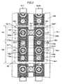
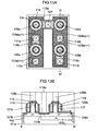
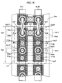
- FIG. 2 is a plane view of an SRAM in Embodiment 1 of the present invention.
- a unit cell UC shown in FIG. 2 is repeatedly arranged in an SRAM cell array.
- FIGS. 3A to 3D show cross-sectional structures at the section lines A-A', B-B', C-C', and D-D' in the layout of FIG. 2 .
- An n- well or a first well 101a is formed on a substrate within an SRAM cell array. Diffusion layers on the substrate are separated by an element separator 102.
- a first memory node Qa1 formed by diffusion layers on the substrate is formed by a first p+ diffusion layer 103a and a first n+ diffusion layer 104a and is connected by a first silicide layer 113a formed on the substrate surface.
- a second memory node Qb1 formed by diffusion layers on the substrate is formed by a second p+ diffusion layer 103b and a second n+ diffusion layer 104b and is connected by a second silicide layer 113b formed on the substrate surface.
- a first anti-leak diffusion layer 101b or second anti-leak diffusion layer 101c consisting of a p+ diffusion layer is formed between the first well 101a and first n+ diffusion layer 104a.
- the first anti-leak diffusion layer 101b and second anti-leak diffusion layer 101c are each separated by the element separator 102 in each diffusion layer on the substrate.
- Qp11 and Qp21 are PMOS access transistors for accessing the memory cell.
- Qn11 and Qn21 are NMOS driver transistors for driving the memory cell.
- one unit cell UC comprises transistors arranged in two rows and two columns on the substrate. Arranged in the first column, the access transistor Qp11 and driver transistor Qn11 are provided on the first memory node Qa1 in this order from the top in the figure. Arranged in the second column, the access transistor Qp21 and driver transistor Qn21 are provided on the second memory node Qb in this order from the top in the figure.
- the SRAM cell array of this embodiment is constructed by successively arranging the unit cells UC having such four transistors in the vertical direction in the figure.
- a contact 110a formed on the first memory node Qa1 is connected to a contact 111b formed on a gate wire extending from the gate electrode of the driver transistor Qn21 by a node connection wire Na1 .
- a contact 110b formed on the second memory node Qb1 is connected to a contact 111a formed on a gate wire extending from the gate electrode of the driver transistor Qn11 by a node connection wire Nb1 .
- a contact 106a formed in the upper part of the access transistor Qp11 is connected to the bit line BL1 .
- a contact 106b formed in the upper part of the access transistor Qp21 is connected to the bit line BLB1 .
- a common contact 107 formed on a gate wire extending from the gate electrodes of the access transistor Qp11 and access transistor Qp21 is connected to the word line WL1 .
- the gate wire extending from the gate electrode of an access transistor Qp11 or Qp21 is shared with an adjoining cell in the crosswise direction and a contact on the gate wire is formed between the adjoining cells.
- Contacts ( 108a , 108b) formed in the upper parts of the driver transistors ( Qn11 , Qn21) are connected to the ground potential wiring layer Vss1 . It is desirable that the word line, bit lines, and ground potential wire are connected in a layer above the node connection wires or intra-memory cell wires so as to be shared with the other memory cells.
- the node connection wire (Na1), node connection wire ( Nb1 ), and ground potential wire ( Vss1 ) are provided in a layer below the bit lines ( BL1 , BLB1 ) and the word line ( WL1 ) is provided in a layer above the bit lines ( BL1 , BLB1 ) so that undesired contact between the wires and contacts does not occur.
- FIG. 2 shows an n+ injection region 125 and a p+ injection region 124.
- the pattern for forming the n+ injection region 125 and p+ injection region 124 consists of simple lines and spaces. Therefore, there is very little influence of dimensional variations and misalignment. The dimensional margin around the boundary between the n+ and p+ injection regions 124 and 125 is minimized. In the figure, the vertical length of the SRAM cell (the length in the connection direction of SRAM cells) is effectively reduced.
- the memory nodes Qa1 and Qb1 and gate wires shown in the layout of FIG. 2 are all rectangular in shape. Therefore, the pattern can easily be corrected in shape by OPC (optical proximity correction), which is suitable for attaining a small SRAM cell area.
- OPC optical proximity correction
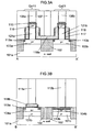
- the source and drain of each transistor composing the SRAM are defined as follows.
- a diffusion layer formed in the upper part of a columnar semiconductor layer connected to a ground voltage is defined as the source diffusion layer and a diffusion layer formed in the lower part of the columnar semiconductor layer is defmed as the drain diffusion layer.
- diffusion layers formed in the upper and lower parts of a columnar semiconductor layer serve either as a source or as a drain depending on the operation state.
- the diffusion layer formed in the upper part of a columnar semiconductor layer is defined as the source diffusion layer and the diffusion layer formed in the lower part of the columnar semiconductor layer is defined as the drain diffusion layer for convenience.
- FIG. 3A an n- well or a first well 101a shared in an SRAM cell array is formed in a substrate and diffusion layers on the substrate are separated by an element separator 102.
- a first p+ drain diffusion layer 103a is formed for the first memory node Qa1 formed by diffusion layers on the substrate by impurity implantation.
- a second p+ drain diffusion layer 103b is formed for the second memory node Qb1 formed by diffusion layers on the substrate by impurity implantation.
- first and second silicide layers are formed on the first and second p+ drain diffusion layers ( 103a , 103b), respectively.
- a columnar silicon layer 121a composing the access transistor Qp11 is formed on the first p+ drain diffusion layer 103a and a columnar silicon layer 121b composing the access transistor Qp21 is formed on the second p+ drain diffusion layer 103b.
- a gate insulating film 117 and a gate electrode 118 are formed around each columnar silicon layer.
- a p+ source diffusion layer 116 is formed in the upper part of the columnar silicon layer by impurity implantation and a silicide layer 115 is formed on the surface of the source diffusion layer.
- a contact 106a formed on the access transistor Qp11 is connected to the bit line BL1 and a contact 106b formed on the access transistor Qp21 is connected to the bit line BLB1 .
- a contact 107 formed on a gate wire 118a extending from the gates of the access transistors Qp11 and Qp21 is connected to the word line WL1 .
- the n- well or the first well 101a shared in the SRAM cell array is formed in the substrate and the diffusion layers on the substrate are separated by the element separator 102.
- a first n+ drain diffusion layer 104a is formed for the first memory node Qa1 formed by diffusion layers on the substrate by impurity implantation and a second n+ drain diffusion layer 104b is formed for the second memory node Qb1 formed by diffusion layers on the substrate by impurity implantation.
- the first and second silicide layers ( 113a , 113b) are formed on the first and second n+ drain diffusion layers ( 104a , 104b), respectively.
- a contact 111a formed on the first n+ drain diffusion layer 104a is formed on around the boundary area between the first p+ drain diffusion layer 103a and first n+ drain diffusion layer 104a and connected to a contact 111a formed on a gate wire 118b extending from the gate electrode of the driver transistor Qn11 via a memory node connection wire Na1 .
- a first anti-leak diffusion layer 101b consisting of a p+ diffusion layer is formed between the first well 101a and first n+ drain diffusion layer 104a .
- a second anti-leak diffusion layer 101c consisting of a p+ diffusion layer is formed between the first well 101a and second n+ drain diffusion layer 104b.
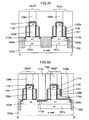
- the n- well or the first well 101a shared in the SRAM cell array is formed in the substrate and the diffusion layers on the substrate are separated by the element separator 102.
- the first n+ drain diffusion layer 104a is formed for the first node Qa1 formed by diffusion layers on the substrate by impurity implantation and the second n+ drain diffusion layer 104b is formed for the second memory node Qb1 formed by diffusion layers on the substrate by impurity implantation.
- the first and second silicide layers (113a, 113b) are formed on the surfaces of the first and second n+ drain diffusion layers ( 104a , 104b), respectively.
- the first anti-leak diffusion layer 101b consisting of a p+ diffusion layer is formed between the first well 101a and first n+ drain diffusion layer 104a . Furthermore, in order to prevent leak from the second n+ drain diffusion layer 104b having the same conductivity type as the first well 101a to the substrate, the second anti-leak diffusion layer 101c consisting of a p+ diffusion layer is formed between the first well 101a and second n+ diffusion layer 104b.
- a columnar silicon layer 122a forming the driver transistor Qn11 is formed on the first n+ drain diffusion layer 104a and a columnar silicon layer 122b forming the driver transistor Qn21 is formed on the second n+ drain diffusion layer 104b.
- a gate insulating film 117 and a gate electrode 118 are formed around each columnar silicon layer.
- An n+ source diffusion layer 114 is formed in the upper part of the columnar silicon layer by impurity implantation and a silicide layer 115 is formed on the surface of the source diffusion layer. Both contacts (108a, 108b) formed on the driver transistors (Qn11, Qn21) are connected to the ground potential Vss1 via a wiring layer.
- the n- well or the first well 101a shared in the SRAM cell array is formed in the substrate and the diffusion layers on the substrate are separated by the element separator 102.
- a second p+ drain diffusion layer 103b and a second n+ drain diffusion layer 104b are formed for the second memory node Qb formed by diffusion layers on the substrate by impurity implantation.
- a second silicide layer 113b is formed on the drain diffusion layer. The second p+ drain diffusion layer 103b and second n+ drain diffusion layer 104b are directly connected by the second silicide layer 113b.
- the second anti-leak diffusion layer 101c consisting of a p+ diffusion layer is formed between the first well 101a and second n+ drain diffusion layer 104b.
- a columnar silicon layer 122b composing the access transistor Qp21 is formed on the second p+ drain diffusion layer 103b and a columnar silicon layer 122b composing the driver transistor Qn21 is formed on the second n+ drain diffusion layer 104b.
- a gate insulating film 117 and a gate electrode 118 are formed around each of the p and n columnar silicon layers.
- a source diffusion layer is formed in the upper part of each columnar silicon layer by impurity implantation.
- a silicide layer 115 is formed on the surface of the source diffusion layer.
- a contact 108b formed on the access transistor Qp21 is connected to the bit line BLB1 and a contact 108b formed on the driver transistor Qn21 is connected to the ground potential Vss1 .
- a contact 110b is formed on a gate wire 118c extending from the gate electrode of the driver transistor Qn21 .
- the contact 110b is connected to a contact 111a formed on the first n+ drain diffusion layer 104a via a memory node connection wire Na1 .
- a contact 111b is formed on the second n+ drain diffusion layer 104b.
- the contact 111b is connected to a contact 111a formed on a gate wire 118b extending from the gate electrode of the driver transistor Qn11 via a memory node connection wire Nb1 .
- the n+ drain diffusion layer and p+ drain diffusion layer forming the memory nodes ( Qa1 , Qb1 ) are directly connected by a silicide layer, whereby the access transistor and driver transistor share a drain diffusion layer and function as a memory node of an SRAM. Therefore, there is no need of forming an element separator separating the n+ drain diffusion layer from the p+ drain diffusion layer. Only the element separator separating two memory nodes of an SRAM is necessary, attaining a small SRAM cell area.
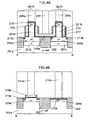
- an SRAM cell having a structure in which a first well 201a is a p- well and a first and second anti-leak diffusion layers 201b and 201c consisting of n+ diffusion layers are formed between an n+ diffusion layer and the substrate can similarly be formed.
- the first anti-leak diffusion layer 201b is formed between a p+ drain diffusion layer 203a and the first well 201a
- the second anti-leak diffusion layer 201c is formed between a p+ drain diffusion layer 203b and the first well 201a so as to prevent leak from the diffusion layer to the substrate.
- FIGS. 5A to 13B An example of a method of producing the semiconductor memory device of the present invention will be described hereafter with reference to FIGS. 5A to 13B .
- A is a plane view and B is a cross-sectional view at a line D-D' in A.
- a silicon nitride film or the like is formed on a substrate, a pattern for columnar silicon layers (121a, 122a , 121b, 122b) is formed by lithography, and etching is performed to form a silicon nitride film mask 119 and columnar silicon layers (121a, 122a , 121b , 122b). Subsequently, an n- well or a first well 101a is formed in an SRAM cell array by impurity implantation.
- an element separator 102 is formed.
- the element separator is formed by first etching a groove pattern, filling the groove pattern with an oxide film by CVD or the like, and removing any extra oxide film on the substrate by dry or wet etching. Consequently, a diffusion layer pattern composing a first memory node Qa1 and a second memory node Qb1 is formed on the substrate.
- impurities are introduced in a p+ injection region 124 and an n+ injection region 125, respectively, by ion implantation to form drain diffusion layers ( 103a , 103b, 104a , 104b) in the lower parts of the columnar silicon layers on the substrate.
- drain diffusion layers 103a , 103b, 104a , 104b
- a second anti-leak diffusion layer 101c or a p+ diffusion layer is formed.
- the second anti-leak diffusion layer 101c can be formed by impurity implantation using a mask for the n+ injection region 125.
- a gate insulating film 117 and a gate conductive film 118 are formed.
- the gate insulating film 117 is formed by an oxide film or High-k film.
- the gate conductive film 118 is formed by a polysilicon or metal film.
- a gate wire pattern is formed by lithography using a resist 133.
- the gate conductive film 117 and gate insulating film 118 are etched using the resist 133 as a mask and the resist 133 is removed. Then, gate wires (118a to 118c) are formed. Then, a mask 119 on the pillars is removed.
- an insulating film such as a silicon nitride film is formed and etched back so that an insulating film 134 such as a silicon nitride film covers the sidewalls of columnar silicon layers and the sidewalls of gate electrodes.
- impurities are introduced in the p+ injection region 124 and n+ injection region 125, respectively, by ion implantation to form source diffusion layers (114, 116) in the upper parts of the columnar silicon layers.
- silicide layers (113a, 113b) on the drain diffusion layers and a silicide layer 115 on the source diffusion layers in the upper parts of the columnar silicon layers are formed by sputtering of a metal such as Ni and heat treatment.
- the insulating film 134 such as a silicon nitride film covering the sidewalls of the columnar silicon layers and gate electrodes prevents any drain-gate or source-gate shortcircuit which may occur due to the silicide layer.
- contacts (106a to 111a, 106b to 111b) are formed after a silicon oxide film or an interlayer film is formed.
- the SRAM cell of the present invention has limitation on layout at many points because of the minimum distance between contacts. Therefore, the contacts on the columnar silicon layers are formed in the first lithography and etching and the contacts on the diffusion layers and gates are formed in the second lithography and etching. In this way, the minimum distance between the contacts on the columnar silicon layers and the contacts on the diffusion layers and gates can be reduced, whereby further reducing the SRAM cell area.
- the contacts on the gates can be formed in the same step as the contacts on the columnar silicon layers.
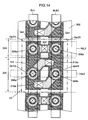
- FIG. 14 is a plane view of the SRAM of Embodiment 2 of the present invention. This embodiment is different from Embodiment 1 in the following point.
- the memory node Qa3 formed by the first diffusion layer on the substrate and the gate wire extending from the gate electrode of the driver transistor Qn23 are connected by a common contact 310a extending over them.
- the memory node Qb3 formed by the second diffusion layer on the substrate and the gate wire extending from the gate electrode of the driver transistor Qn13 are connected by a common contact 310b extending over them.
- the gate and memory node are connected by a contact, not by a wiring layer, as described above; the number of contacts in an SRAM cell can be reduced.
- the cell area can be reduced by adjusting the positions of columnar silicon layers and contacts.
- the word line, bit lines, and ground potential wire are desirably provided in a layer above the node connection wires or intra-memory cell wires so as to be shared with the other memory cells.
- the node connection wires are formed by contacts. Except for this point, the same structure as in Embodiment 1 is employed and further explanation is omitted.
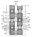
- FIG. 15 is a plane view of the SRAM of Embodiment 3 of the present invention.
- This embodiment is different from Embodiments 1 and 2 in the following point.
- the contact (110a, 210a ) adjoins only the driver transistor ( Qn11 , Qn12 ) on the memory node Qa while the contact (110b, 210b ) are provided on the diffusion layer between the driver transistor (Qn21, Qn22) and access transistor ( Qp21 , Qp22 ) on the memory node Qb.
- This asymmetric layout causes asymmetry in characteristics of the SRAM cell and may narrow the operational margin.
- a vertically (longitudinally) and horizontally (laterally) symmetric layout is employed. Therefore, deterioration in the operational margin due to the above asymmetry does not occur, attaining an SRAM cell having a broad operational margin.
- a memory node Qa4 formed by the first diffusion layer on the substrate and the gate wire extending from the gate electrode of a driver transistor Qn24 are connected by a common contact 410a extending over them.
- a memory node Qb4 formed by the second diffusion layer on the substrate and the gate wire extending from the gate electrode of a driver transistor Qn14 are connected by a common contact 410b extending over them.
- the word line, bit lines, and ground potential wire are desirably provided in a layer above the node connection wires or intra-memory cell wires so as to be shared with the other memory cells.
- the node connection wires are formed by contacts.
- a ground potential wire Vss4 and a word line WL4 are provided in the same layer and bit lines (BL4, BLB4) are provided in a layer above the word line WL4 so that undesired contact between the wires and contacts does not occur.
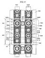
- FIG. 16 is a plane view of the SRAM of Embodiment 4 of the present invention.
- a vertically (longitudinally) and horizontally (laterally) symmetric layout is used as in Embodiment 3 and, therefore, the above problems due to asymmetry do not occur. Then, an SRAM cell having a broader operational margin can be attained.
- the word line, bit lines, and ground potential wire are desirably provided in a layer above the node connection wires or intra-memory cell wires so as to be shared with the other memory cells.
- a node connection wire (Na5), node connection wire (Nb5), and ground potential wire ( Vss5 ) are provided in a lower layer than a word line ( WL5 ), and bit lines (BL5, BLB5) are provided in an upper layer than the word line ( WL5 ) so that undesired contact between the wires and contacts does not occur.
- FIG. 17 is a plane view of the SRAM of Embodiment 5 of the present invention.
- This embodiment is different from Embodiment 1 in that the columnar silicon layers forming access transistors are different in shape and the columnar silicon layers forming driver transistor are different in size.
- the leak current of access transistors should be larger than the leak current of driver transistors.
- the leak current of access transistors can be increased by enlarging the columnar silicon layers forming access transistors as shown in FIG. 17 .
- the columnar silicon layers of driver transistors are enlarged so as to increase the current of the driver transistors, whereby the reading margin can be improved
- Embodiment 1 the same layout as in Embodiment 1 is employed by way of example. In practice, it is not restricted to the layout of Embodiment 1 and this embodiment can similarly apply to the layouts of the other embodiments.
- the word line, bit lines, power supply potential wire, and ground potential wire are desirably provided in a layer above the node connection wires or intra-memory cell wires so as to be shared with the other memory cells.
- the same hierarchical wire configuration as in Embodiment 1 can be attained. Except for this point, the same structure as in Embodiment 1 is employed and further explanation is omitted.
- FIG. 18 is a plane view of the SRAM of Embodiment 6 of the present invention. This embodiment is different from Embodiment 1 in the flowing point.
- the cells, at immediately upper and lower positions in the plane of the sheet face of the figure, of the SRAM cell shown as the unit cell UC are inverted from Embodiment 1.
- Contacts ( 706a, 706b ) formed on access transistors ( Qb17, Qb27 ) and connected to bit lines are common contacts also used as the contacts of the SRAM cell, at immediately upper positions in the plane of the sheet face of the figure, that are connected to the bit lines.
- this SRAM cell has the same layout as of Embodiment 1.
- Embodiment 1 the same layout as in Embodiment 1 is employed by way of example. In practice, it is not restricted to the layout of Embodiment 1 and this embodiment can similarly apply to the layouts of the other embodiments.
- the word line, bit lines, power supply potential wire, and ground potential wire are desirably provided in a layer above the node connection wires or intra-memory cell wires so as to be shared with the other memory cells.
- the same hierarchical wire configuration as in Embodiment 1 can be attained. Except for this point, the same structure as in Embodiment 1 is employed and further explanation is omitted.
Description
- The present invention relates generally to a semiconductor memory device and particularly to a semiconductor memory device composed of an SRAM (static random access memory).
- SGT (surrounding gate transistor) technologies are known as measures for attaining higher levels of integration and performance in semiconductor devices (disclosed for example in Unexamined Japanese Patent Application KOKAI Publication Nos.
H2-188966 H7-99311 - With the increasingly strong demands in recent years for large capacity SRAMs installed in LSIs (large-scale integrated circuits), it is desired to realize an SRAM having a small cell area with the use of SGTs.
-
FIG. 19A is a plane view of a CMOS 6T-SRAM memory cell composed of six SGTs, which is shown in an embodiment of Unexamined Japanese Patent Application KOKAI Publication No.H7-99311 FIG. 19B is a cross-sectional view at A-A' inFIG. 19A . In these figures, bit lines (801a, 801b) are formed by an n+ diffusion layer, a ground potential wire GND is formed by ann+ diffusion layer 802, and a power supply potential wire Vcc is formed by ap+ diffusion layer 803. - Columnar silicon layers composing access transistors (810a, 810b) for accessing the memory cell, driver transistors (811a, 811b) for driving the memory cell, and load transistors (812a, 812b) for supplying charge to the memory cell, respectively, are formed on these diffusion layers. Gates (804a, 804b, 804c, 804d) are formed around the columnar silicon layers. Memory nodes are composed of wiring layers (807a, 807b).
In the above memory cell (SRAM cell), the transistors each have the source, gate, and drain arranged vertically on the columnar silicon layer. Therefore, a small SRAM cell can be designed. - The above SRAM cell can attain a small cell area when the power supply
potential wire 803 and groundpotential wire 802 have approximately the minimum dimensions. However, the power supplypotential wire 803 and groundpotential wire 802 are formed by a p+ diffusion layer and an n+ diffusion layer, respectively. Therefore, they have significantly high resistance and it is difficult to achieve high SRAM operation speeds when they have approximately the minimum dimensions. On the other hand, when the power supplypotential wire 803 and groundpotential wire 802 are increased in dimension for high SRAM operation speeds, the SRAM cell has a larger area. - In SRAMs using conventional planar transistors, the power supply potential wire and ground potential wire are formed by low resistant Cu wires. Therefore, it is essential to form the power supply potential wire and ground potential wire by Cu wires in order for SRAMs using SGTs to achieve operation speeds equivalent to those of SRAMs using planar transistors.
- Loadless 4T-SRAMs have been proposed as an SRAM having an SRAM cell area smaller than CMOS 6T-SRAMs (disclosed for example in Unexamined Japanese Patent Application KOKAI Publication No.
2000-12705 FIG. 1 shows an equivalent circuit to a memory cell of the loadless 4T-SRAM. This SRAM cell is composed of a total of four transistors: two PMOS access transistors (Qp11, Qp21) for accessing the memory and two NMOS driver transistors (Qn11, Qn21) for driving the memory. - Data holding operation in the case wherein data "L" is stored in a memory node Qa1 and data "H" is stored in a memory node Qb1 will be described hereafter as an example of operation of the memory cell in
FIG. 1 . A word line WL1 and bit lines BL1 and BLB1 all have a potential "H" while data is held. The threshold of the access transistors (Qp11, Qp21) is lower than the threshold of the driver transistors (Qn11, Qn21). The off-leak current of the access transistors (Qp11, Qp21) is, for example, approximately 10 to 1000 times larger in average than the off-leak current of the driver transistors (Qn11, Qn21). Therefore, the level "H" of the memory node Qb1 is held by an off-leak current running from the bit line BLB1 to the memory node Qb1 via the access transistor Qp21. On the other hand, the level "L" of the memory node Qa1 is stably held by the driver transistor Qn11. - The above loadless 4T-SRAM can attain a smaller SRAM cell area than CMOS 6T-SRAMs even with the use of SGTs.
-
WO 2009/096466 A1 discloses a Loadless 4T-SRAM comprising vertical transistors formed as SGTs on a SOI-type substrate, with the aim of achieving a sufficiently small SRAM cell area while ensuring a stable operation margin thereof. -
US 4 670 768 A discloses a CMOS inverter comprising vertical channel FETs formed either on a SOI-type substrate or on a bulk substrate, with the aim of achieving a high integration and efficiently preventing the occurrence of a latch-up. -
US 5 293 053 A discloses an elevated CMOS inverter comprising vertical transistors formed on a bulk substrate, with the aim of achieving a high integration and minimizing the risk of a latch-up. - The present invention is made in view of the above circumstances and it is an object of the present invention is to attain an SRAM cell having a small area and sufficient operational margin in a loadless 4T-SRAM using SGTs.
- This object is achieved by a semiconductor memory device as claimed in
claim 1 and a method of producing such semiconductor memory device as claimed in claim 12. - A more complete understanding of this application can be obtained when the following detailed description is considered in conjunction with the following drawings, in which:
-
FIG. 1 is an equivalent circuit showing an SRAM according toEmbodiment 1 of the present invention; -
FIG. 2 is a plane view of the SRAM according toEmbodiment 1 of the present invention; -
FIG. 3A is a cross-sectional view of the SRAM according toEmbodiment 1 of the present invention; -
FIG. 3B is a cross-sectional view of the SRAM according toEmbodiment 1 of the present invention; -
FIG. 3C is a cross-sectional view of the SRAM according toEmbodiment 1 of the present invention; -
FIG. 3D is a cross-sectional view of the SRAM according toEmbodiment 1 of the present invention; -
FIG. 4A is a cross-sectional view of another SRAM according toEmbodiment 1 of the present invention; -
FIG. 4B is a cross-sectional view of another SRAM according toEmbodiment 1 of the present invention; -
FIG. 4C is a cross-sectional view of another SRAM according toEmbodiment 1 of the present invention; -
FIG. 4D is a cross-sectional view of another SRAM according toEmbodiment 1 of the present invention; -
FIG. 5A is a plane view showing a production step (1) of the SRAM according toEmbodiment 1 of the present invention; -
FIG. 5B is a cross-sectional view showing the production step (1) of the SRAM according toEmbodiment 1 of the present invention; -
FIG. 6A is a plane view showing a production step (2) of the SRAM according toEmbodiment 1 of the present invention; -
FIG. 6B is a cross-sectional view showing the production step (2) of the SRAM according toEmbodiment 1 of the present invention; -
FIG. 7A is a plane view showing a production step (3) of the SRAM according toEmbodiment 1 of the present invention; -
FIG. 7B is a cross-sectional view showing the production step (3) of the SRAM according toEmbodiment 1 of the present invention; -
FIG. 8A is a plane view showing a production step (4) of the SRAM according toEmbodiment 1 of the present invention; -
FIG. 8B is a cross-sectional view showing the production step (4) of the SRAM according toEmbodiment 1 of the present invention; -
FIG. 9A is a plane view showing a production step (5) of the SRAM according toEmbodiment 1 of the present invention; -
FIG. 9B is a cross-sectional view showing the production step (5) of the SRAM according toEmbodiment 1 of the present invention; -
FIG. 10A is a plane view showing a production step (6) of the SRAM according toEmbodiment 1 of the present invention; -
FIG. 10B is a cross-sectional view showing the production step (6) of the SRAM according toEmbodiment 1 of the present invention; -
FIG. 11A is a plane view showing a production step (7) of the SRAM according toEmbodiment 1 of the present invention; -
FIG. 11B is a cross-sectional view showing the production step (7) of the SRAM according toEmbodiment 1 of the present invention; -
FIG. 12A is a plane view showing a production step (8) of the SRAM according toEmbodiment 1 of the present invention; -
FIG. 12B is a cross-sectional view showing the production step (8) of the SRAM according toEmbodiment 1 of the present invention; -
FIG. 13A is a plane view showing a production step (9) of the SRAM according toEmbodiment 1 of the present invention; -
FIG. 13B is a cross-sectional view showing the production step (9) of the SRAM according toEmbodiment 1 of the present invention; -
FIG. 14 is a plane view of an SRAM according to Embodiment 2 of the present invention; -
FIG. 15 is a plane view of an SRAM according to Embodiment 3 of the present invention; -
FIG. 16 is a plane view of an SRAM according to Embodiment 4 of the present invention; -
FIG. 17 is a plane view of an SRAM according to Embodiment 5 of the present invention; -
FIG. 18 is a plane view of an SRAM according to Embodiment 6 of the present invention; -
FIG. 19A is a plane view of a prior art SRAM using SGTs; and -
FIG. 19B is a cross-sectional view of the prior art SRAM using SGTs. - Embodiments of the present invention will be described hereafter in detail with reference to the drawings. In the embodiments below, it is assumed that the semiconductor memory device of the present invention is constructed by a loadless 4T-SRAM.
-
FIG. 1 shows an equivalent circuit to a memory cell (SRAM cell) that constitutes a loadless 4T-SRAM cell according toEmbodiment 1. InFIG. 1 , BL1 and BLB1 are bit lines, WL1 is a word line, Vss1 is a ground potential, Qp11 and Qp21 are access transistors, Qn11 and Qn21 are driver transistors, and Qa1 and Qb1 are memory nodes for storing data. The access transistors Qp11 and Qp21 have functions of accessing the memory cell and charging memory nodes to "H." The driver transistors Qn11 and Qn21 drive the memory nodes to read and write memory cell data. -
FIG. 2 is a plane view of an SRAM inEmbodiment 1 of the present invention. A unit cell UC shown inFIG. 2 is repeatedly arranged in an SRAM cell array.FIGS. 3A to 3D show cross-sectional structures at the section lines A-A', B-B', C-C', and D-D' in the layout ofFIG. 2 . - First, the layout of this embodiment will be described with reference to
FIGS. 2 and3A to 3D . An n- well or afirst well 101a is formed on a substrate within an SRAM cell array. Diffusion layers on the substrate are separated by anelement separator 102. A first memory node Qa1 formed by diffusion layers on the substrate is formed by a firstp+ diffusion layer 103a and a firstn+ diffusion layer 104a and is connected by afirst silicide layer 113a formed on the substrate surface. Similarly, a second memory node Qb1 formed by diffusion layers on the substrate is formed by a secondp+ diffusion layer 103b and a secondn+ diffusion layer 104b and is connected by asecond silicide layer 113b formed on the substrate surface.
In order to prevent leak from the firstn+ diffusion layer 104a having the same conductivity type as the n- well or thefirst well 101a to the substrate, a firstanti-leak diffusion layer 101b or secondanti-leak diffusion layer 101c consisting of a p+ diffusion layer is formed between thefirst well 101a and firstn+ diffusion layer 104a. The firstanti-leak diffusion layer 101b and secondanti-leak diffusion layer 101c are each separated by theelement separator 102 in each diffusion layer on the substrate. - Qp11 and Qp21 are PMOS access transistors for accessing the memory cell. Qn11 and Qn21 are NMOS driver transistors for driving the memory cell.
- In this embodiment, one unit cell UC comprises transistors arranged in two rows and two columns on the substrate. Arranged in the first column, the access transistor Qp11 and driver transistor Qn11 are provided on the first memory node Qa1 in this order from the top in the figure. Arranged in the second column, the access transistor Qp21 and driver transistor Qn21 are provided on the second memory node Qb in this order from the top in the figure. The SRAM cell array of this embodiment is constructed by successively arranging the unit cells UC having such four transistors in the vertical direction in the figure.
- A
contact 110a formed on the first memory node Qa1 is connected to acontact 111b formed on a gate wire extending from the gate electrode of the driver transistor Qn21 by a node connection wire Na1. Acontact 110b formed on the second memory node Qb1 is connected to acontact 111a formed on a gate wire extending from the gate electrode of the driver transistor Qn11 by a node connection wire Nb1. Acontact 106a formed in the upper part of the access transistor Qp11 is connected to the bit line BL1. Acontact 106b formed in the upper part of the access transistor Qp21 is connected to the bit line BLB1. Acommon contact 107 formed on a gate wire extending from the gate electrodes of the access transistor Qp11 and access transistor Qp21 is connected to the word line WL1. Here, it is possible that the gate wire extending from the gate electrode of an access transistor Qp11 or Qp21 is shared with an adjoining cell in the crosswise direction and a contact on the gate wire is formed between the adjoining cells. - Contacts (108a, 108b) formed in the upper parts of the driver transistors (Qn11, Qn21) are connected to the ground potential wiring layer Vss1. It is desirable that the word line, bit lines, and ground potential wire are connected in a layer above the node connection wires or intra-memory cell wires so as to be shared with the other memory cells.
- In a realizable configuration of the above hierarchical wiring, the node connection wire (Na1), node connection wire (Nb1), and ground potential wire (Vss1) are provided in a layer below the bit lines (BL1, BLB1) and the word line (WL1) is provided in a layer above the bit lines (BL1, BLB1) so that undesired contact between the wires and contacts does not occur.
-
FIG. 2 shows ann+ injection region 125 and ap+ injection region 124. In the SRAM cell array region of this embodiment, the pattern for forming then+ injection region 125 andp+ injection region 124 consists of simple lines and spaces. Therefore, there is very little influence of dimensional variations and misalignment. The dimensional margin around the boundary between the n+ andp+ injection regions - Furthermore, in this embodiment, the memory nodes Qa1 and Qb1 and gate wires shown in the layout of
FIG. 2 are all rectangular in shape. Therefore, the pattern can easily be corrected in shape by OPC (optical proximity correction), which is suitable for attaining a small SRAM cell area. - In the present invention, the source and drain of each transistor composing the SRAM are defined as follows. For the driver transistors (Qn11, Qn21), a diffusion layer formed in the upper part of a columnar semiconductor layer connected to a ground voltage is defined as the source diffusion layer and a diffusion layer formed in the lower part of the columnar semiconductor layer is defmed as the drain diffusion layer. For the access transistors (Qp11, Qp21), diffusion layers formed in the upper and lower parts of a columnar semiconductor layer serve either as a source or as a drain depending on the operation state. Here, the diffusion layer formed in the upper part of a columnar semiconductor layer is defined as the source diffusion layer and the diffusion layer formed in the lower part of the columnar semiconductor layer is defined as the drain diffusion layer for convenience.
- The SRAM structure of the present invention will be described hereafter with reference to the cross-sectional structures in
FIGS. 3A to 3D . As shown inFIG. 3A , an n- well or afirst well 101a shared in an SRAM cell array is formed in a substrate and diffusion layers on the substrate are separated by anelement separator 102. A first p+drain diffusion layer 103a is formed for the first memory node Qa1 formed by diffusion layers on the substrate by impurity implantation. A second p+drain diffusion layer 103b is formed for the second memory node Qb1 formed by diffusion layers on the substrate by impurity implantation. Furthermore, first and second silicide layers (113a, 113b) are formed on the first and second p+ drain diffusion layers (103a, 103b), respectively. Acolumnar silicon layer 121a composing the access transistor Qp11 is formed on the first p+drain diffusion layer 103a and acolumnar silicon layer 121b composing the access transistor Qp21 is formed on the second p+drain diffusion layer 103b. - A
gate insulating film 117 and agate electrode 118 are formed around each columnar silicon layer. A p+source diffusion layer 116 is formed in the upper part of the columnar silicon layer by impurity implantation and asilicide layer 115 is formed on the surface of the source diffusion layer. Acontact 106a formed on the access transistor Qp11 is connected to the bit line BL1 and acontact 106b formed on the access transistor Qp21 is connected to the bit line BLB1. Acontact 107 formed on agate wire 118a extending from the gates of the access transistors Qp11 and Qp21 is connected to the word line WL1. - As shown in
FIG. 3B , the n- well or thefirst well 101a shared in the SRAM cell array is formed in the substrate and the diffusion layers on the substrate are separated by theelement separator 102. A first n+drain diffusion layer 104a is formed for the first memory node Qa1 formed by diffusion layers on the substrate by impurity implantation and a second n+drain diffusion layer 104b is formed for the second memory node Qb1 formed by diffusion layers on the substrate by impurity implantation. Furthermore, the first and second silicide layers (113a, 113b) are formed on the first and second n+ drain diffusion layers (104a, 104b), respectively. Acontact 111a formed on the first n+drain diffusion layer 104a is formed on around the boundary area between the first p+drain diffusion layer 103a and first n+drain diffusion layer 104a and connected to acontact 111a formed on agate wire 118b extending from the gate electrode of the driver transistor Qn11 via a memory node connection wire Na1. - In order to prevent leak from the first n+
drain diffusion layer 104a having the same conductivity type as thefirst well 101a to the substrate, a firstanti-leak diffusion layer 101b consisting of a p+ diffusion layer is formed between thefirst well 101a and first n+drain diffusion layer 104a. In order to prevent leak from the second n+drain diffusion layer 104b having the same conductivity type as thefirst well 101a to the substrate, a secondanti-leak diffusion layer 101c consisting of a p+ diffusion layer is formed between thefirst well 101a and second n+drain diffusion layer 104b. - As shown in
FIG. 3C , the n- well or thefirst well 101a shared in the SRAM cell array is formed in the substrate and the diffusion layers on the substrate are separated by theelement separator 102. The first n+drain diffusion layer 104a is formed for the first node Qa1 formed by diffusion layers on the substrate by impurity implantation and the second n+drain diffusion layer 104b is formed for the second memory node Qb1 formed by diffusion layers on the substrate by impurity implantation. Furthermore, the first and second silicide layers (113a, 113b) are formed on the surfaces of the first and second n+ drain diffusion layers (104a, 104b), respectively. The firstanti-leak diffusion layer 101b consisting of a p+ diffusion layer is formed between thefirst well 101a and first n+drain diffusion layer 104a. Furthermore, in order to prevent leak from the second n+drain diffusion layer 104b having the same conductivity type as thefirst well 101a to the substrate, the secondanti-leak diffusion layer 101c consisting of a p+ diffusion layer is formed between thefirst well 101a and secondn+ diffusion layer 104b. - A
columnar silicon layer 122a forming the driver transistor Qn11 is formed on the first n+drain diffusion layer 104a and acolumnar silicon layer 122b forming the driver transistor Qn21 is formed on the second n+drain diffusion layer 104b. Agate insulating film 117 and agate electrode 118 are formed around each columnar silicon layer. An n+source diffusion layer 114 is formed in the upper part of the columnar silicon layer by impurity implantation and asilicide layer 115 is formed on the surface of the source diffusion layer. Both contacts (108a, 108b) formed on the driver transistors (Qn11, Qn21) are connected to the ground potential Vss1 via a wiring layer. - As shown in
FIG. 3D , the n- well or thefirst well 101a shared in the SRAM cell array is formed in the substrate and the diffusion layers on the substrate are separated by theelement separator 102. A second p+drain diffusion layer 103b and a second n+drain diffusion layer 104b are formed for the second memory node Qb formed by diffusion layers on the substrate by impurity implantation. Asecond silicide layer 113b is formed on the drain diffusion layer. The second p+drain diffusion layer 103b and second n+drain diffusion layer 104b are directly connected by thesecond silicide layer 113b. Therefore, there is no need of forming an element separator separating the n+ drain diffusion layer from the p+ drain diffusion layer or a contact connecting the n+ drain diffusion layer to the p+ drain diffusion layer. Then, the memory cell area can be reduced. In order to prevent leak from the secondn+ diffusion layer 104b having the same conductivity type as thefirst well 101a to the substrate, the secondanti-leak diffusion layer 101c consisting of a p+ diffusion layer is formed between thefirst well 101a and second n+drain diffusion layer 104b. - A
columnar silicon layer 122b composing the access transistor Qp21 is formed on the second p+drain diffusion layer 103b and acolumnar silicon layer 122b composing the driver transistor Qn21 is formed on the second n+drain diffusion layer 104b. Agate insulating film 117 and agate electrode 118 are formed around each of the p and n columnar silicon layers. A source diffusion layer is formed in the upper part of each columnar silicon layer by impurity implantation. Asilicide layer 115 is formed on the surface of the source diffusion layer. Acontact 108b formed on the access transistor Qp21 is connected to the bit line BLB1 and acontact 108b formed on the driver transistor Qn21 is connected to the ground potential Vss1. - A
contact 110b is formed on agate wire 118c extending from the gate electrode of the driver transistor Qn21. Thecontact 110b is connected to acontact 111a formed on the first n+drain diffusion layer 104a via a memory node connection wire Na1. Acontact 111b is formed on the second n+drain diffusion layer 104b. Thecontact 111b is connected to acontact 111a formed on agate wire 118b extending from the gate electrode of the driver transistor Qn11 via a memory node connection wire Nb1. - As described above, in the present invention, the n+ drain diffusion layer and p+ drain diffusion layer forming the memory nodes (Qa1, Qb1) are directly connected by a silicide layer, whereby the access transistor and driver transistor share a drain diffusion layer and function as a memory node of an SRAM. Therefore, there is no need of forming an element separator separating the n+ drain diffusion layer from the p+ drain diffusion layer. Only the element separator separating two memory nodes of an SRAM is necessary, attaining a small SRAM cell area.
- As shown in
FIGS. 4A to 4D , an SRAM cell having a structure in which afirst well 201a is a p- well and a first and second anti-leak diffusion layers 201b and 201c consisting of n+ diffusion layers are formed between an n+ diffusion layer and the substrate can similarly be formed. In such a case, the firstanti-leak diffusion layer 201b is formed between a p+drain diffusion layer 203a and thefirst well 201a and the secondanti-leak diffusion layer 201c is formed between a p+drain diffusion layer 203b and thefirst well 201a so as to prevent leak from the diffusion layer to the substrate. - An example of a method of producing the semiconductor memory device of the present invention will be described hereafter with reference to
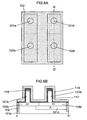
FIGS. 5A to 13B . In each figure, A is a plane view and B is a cross-sectional view at a line D-D' in A. - As shown in
FIGS. 5A and 5B , a silicon nitride film or the like is formed on a substrate, a pattern for columnar silicon layers (121a, 122a, 121b, 122b) is formed by lithography, and etching is performed to form a siliconnitride film mask 119 and columnar silicon layers (121a, 122a, 121b, 122b). Subsequently, an n- well or afirst well 101a is formed in an SRAM cell array by impurity implantation. - As shown in
FIGS. 6A and 6B , anelement separator 102 is formed. The element separator is formed by first etching a groove pattern, filling the groove pattern with an oxide film by CVD or the like, and removing any extra oxide film on the substrate by dry or wet etching. Consequently, a diffusion layer pattern composing a first memory node Qa1 and a second memory node Qb1 is formed on the substrate. - As shown in
FIGS. 7A and 7B , impurities are introduced in ap+ injection region 124 and ann+ injection region 125, respectively, by ion implantation to form drain diffusion layers (103a, 103b, 104a, 104b) in the lower parts of the columnar silicon layers on the substrate. In order to prevent leak from the n+drain diffusion layer 104b having the same conductivity type as the n- well or thefirst well 101a to the substrate, a secondanti-leak diffusion layer 101c or a p+ diffusion layer is formed. The secondanti-leak diffusion layer 101c can be formed by impurity implantation using a mask for then+ injection region 125. - As shown in
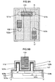
FIGS. 8A and 8B , agate insulating film 117 and a gateconductive film 118 are formed. Thegate insulating film 117 is formed by an oxide film or High-k film. The gateconductive film 118 is formed by a polysilicon or metal film. - As shown in
FIGS. 9A and 9B , a gate wire pattern is formed by lithography using a resist 133. - As shown in
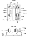
FIGS. 10A and 10B , the gateconductive film 117 andgate insulating film 118 are etched using the resist 133 as a mask and the resist 133 is removed. Then, gate wires (118a to 118c) are formed. Then, amask 119 on the pillars is removed. - As shown in
FIGS. 11A and 11B , an insulating film such as a silicon nitride film is formed and etched back so that an insulatingfilm 134 such as a silicon nitride film covers the sidewalls of columnar silicon layers and the sidewalls of gate electrodes. - As shown in
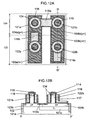
FIGS. 12A ad 12B, impurities are introduced in thep+ injection region 124 andn+ injection region 125, respectively, by ion implantation to form source diffusion layers (114, 116) in the upper parts of the columnar silicon layers. Subsequently, silicide layers (113a, 113b) on the drain diffusion layers and asilicide layer 115 on the source diffusion layers in the upper parts of the columnar silicon layers are formed by sputtering of a metal such as Ni and heat treatment. - Here, the insulating
film 134 such as a silicon nitride film covering the sidewalls of the columnar silicon layers and gate electrodes prevents any drain-gate or source-gate shortcircuit which may occur due to the silicide layer. - As shown in
FIGS. 13A and 13B , contacts (106a to 111a, 106b to 111b) are formed after a silicon oxide film or an interlayer film is formed. - The SRAM cell of the present invention has limitation on layout at many points because of the minimum distance between contacts. Therefore, the contacts on the columnar silicon layers are formed in the first lithography and etching and the contacts on the diffusion layers and gates are formed in the second lithography and etching. In this way, the minimum distance between the contacts on the columnar silicon layers and the contacts on the diffusion layers and gates can be reduced, whereby further reducing the SRAM cell area. Here, the contacts on the gates can be formed in the same step as the contacts on the columnar silicon layers.
-
FIG. 14 is a plane view of the SRAM of Embodiment 2 of the present invention. This embodiment is
different fromEmbodiment 1 in the following point. In Embodiment 2, the memory node Qa3 formed by the first diffusion layer on the substrate and the gate wire extending from the gate electrode of the driver transistor Qn23 are connected by acommon contact 310a extending over them. Furthermore, the memory node Qb3 formed by the second diffusion layer on the substrate and the gate wire extending from the gate electrode of the driver transistor Qn13 are connected by acommon contact 310b extending over them.
The gate and memory node are connected by a contact, not by a wiring layer, as described above; the number of contacts in an SRAM cell can be reduced. The cell area can be reduced by adjusting the positions of columnar silicon layers and contacts. - As mentioned in
Embodiment 1, the word line, bit lines, and ground potential wire are desirably provided in a layer above the node connection wires or intra-memory cell wires so as to be shared with the other memory cells. In this embodiment, the node connection wires are formed by contacts. Except for this point, the same structure as inEmbodiment 1 is employed and further explanation is omitted. -
FIG. 15 is a plane view of the SRAM of Embodiment 3 of the present invention. This embodiment is different fromEmbodiments 1 and 2 in the following point. InEmbodiments 1 and 2, the contact (110a, 210a) adjoins only the driver transistor (Qn11, Qn12) on the memory node Qa while the contact (110b, 210b) are provided on the diffusion layer between the driver transistor (Qn21, Qn22) and access transistor (Qp21, Qp22) on the memory node Qb.
This asymmetric layout causes asymmetry in characteristics of the SRAM cell and may narrow the operational margin. In this embodiment, a vertically (longitudinally) and horizontally (laterally) symmetric layout is employed. Therefore, deterioration in the operational margin due to the above asymmetry does not occur, attaining an SRAM cell having a broad operational margin. - Furthermore, as in Embodiment 2, a memory node Qa4 formed by the first diffusion layer on the substrate and the gate wire extending from the gate electrode of a driver transistor Qn24 are connected by a
common contact 410a extending over them. A memory node Qb4 formed by the second diffusion layer on the substrate and the gate wire extending from the gate electrode of a driver transistor Qn14 are connected by acommon contact 410b extending over them. - The word line, bit lines, and ground potential wire are desirably provided in a layer above the node connection wires or intra-memory cell wires so as to be shared with the other memory cells. In this embodiment, the node connection wires are formed by contacts.
- By way of example in a realizable configuration of the above hierarchical wiring, a ground potential wire Vss4 and a word line WL4 are provided in the same layer and bit lines (BL4, BLB4) are provided in a layer above the word line WL4 so that undesired contact between the wires and contacts does not occur.
-
FIG. 16 is a plane view of the SRAM of Embodiment 4 of the present invention. In this embodiment, a vertically (longitudinally) and horizontally (laterally) symmetric layout is used as in Embodiment 3 and, therefore, the above problems due to asymmetry do not occur. Then, an SRAM cell having a broader operational margin can be attained. The word line, bit lines, and ground potential wire are desirably provided in a layer above the node connection wires or intra-memory cell wires so as to be shared with the other memory cells. - By way of example in a realizable configuration of the above hierarchical wiring, a node connection wire (Na5), node connection wire (Nb5), and ground potential wire (Vss5) are provided in a lower layer than a word line (WL5), and bit lines (BL5, BLB5) are provided in an upper layer than the word line (WL5) so that undesired contact between the wires and contacts does not occur.
-
FIG. 17 is a plane view of the SRAM of Embodiment 5 of the present invention. This embodiment is different fromEmbodiment 1 in that the columnar silicon layers forming access transistors are different in shape and the columnar silicon layers forming driver transistor are different in size. In the loadless 4T-SRAM of the present invention, the leak current of access transistors should be larger than the leak current of driver transistors. The leak current of access transistors can be increased by enlarging the columnar silicon layers forming access transistors as shown inFIG. 17 . - On the other hand, for improving the reading margin, the columnar silicon layers of driver transistors are enlarged so as to increase the current of the driver transistors, whereby the reading margin can be improved,
- In this embodiment, the same layout as in
Embodiment 1 is employed by way of example. In practice, it is not restricted to the layout ofEmbodiment 1 and this embodiment can similarly apply to the layouts of the other embodiments. - As mentioned in
Embodiment 1, the word line, bit lines, power supply potential wire, and ground potential wire are desirably provided in a layer above the node connection wires or intra-memory cell wires so as to be shared with the other memory cells. In this regard, for example, the same hierarchical wire configuration as inEmbodiment 1 can be attained. Except for this point, the same structure as inEmbodiment 1 is employed and further explanation is omitted. -
FIG. 18 is a plane view of the SRAM of Embodiment 6 of the present invention. This embodiment is different fromEmbodiment 1 in the flowing point. In this embodiment, the cells, at immediately upper and lower positions in the plane of the sheet face of the figure, of the SRAM cell shown as the unit cell UC are inverted fromEmbodiment 1. Contacts (706a, 706b) formed on access transistors (Qb17, Qb27) and connected to bit lines are common contacts also used as the contacts of the SRAM cell, at immediately upper positions in the plane of the sheet face of the figure, that are connected to the bit lines. With the contacts connected to the bit lines being shared with an adjoining cell in this way, the contacts (706a, 706b) can be increased in size and easy to form. Furthermore, the contacts have reduced resistance. Other than the contacts (706a, 706b), this SRAM cell has the same layout as ofEmbodiment 1. - In this embodiment, the same layout as in
Embodiment 1 is employed by way of example. In practice, it is not restricted to the layout ofEmbodiment 1 and this embodiment can similarly apply to the layouts of the other embodiments. - As mentioned in
Embodiment 1, the word line, bit lines, power supply potential wire, and ground potential wire are desirably provided in a layer above the node connection wires or intra-memory cell wires so as to be shared with the other memory cells. In this regard, for example, the same hierarchical wire configuration as inEmbodiment 1 can be attained. Except for this point, the same structure as inEmbodiment 1 is employed and further explanation is omitted. -
- 101a, 201a: first well
- 101b, 201b: first anti-leak diffusion layer
- 101c, 201c: second anti-leak diffusion layer
- 102, 202, 302, 402, 502, 602, 702: element separator
- 106a, 206a, 306a, 406a, 506a, 606a, 706a, 106b, 206b, 306b, 406b, 506b, 606b, 706b: contact on access transistor columnar silicon layer
- 107, 207, 307, 407, 507a, 507b, 607, 707: contact on access transistor gate wire
- 108a, 208a, 308a, 408a, 508a, 608a, 708a, 108b, 208b, 308b, 408b, 508b, 608b, 708b: contact on driver transistor columnar silicon layer
- 110a, 210a, 310a, 410a, 510a, 610a, 710a, 110b, 210b, 310b, 410b, 510b, 610b, 710b: contact on memory node
- 111a, 211a, 511a, 611a, 711a, 111b, 211b, 511b, 611b, 711b: contact on gate wire
- 113a, 113b, 115, 213a, 213b, 215: silicide layer
- 114, 214, n+ source diffusion layer
- 116, 216: p+ source diffusion layer
- 117, 217: gate insulating film
- 118, 218, 804a, 804b, 804c, 804d: gate electrode
- 118a, 118b, 118c, 218a, 218b, 218c: gate wire
- 119: mask layer such as silicon oxide film
- 120: silicon layer
- 121a, 121b, 810a, 810b: access transistor columnar silicon layer
- 122a, 122b, 811a, 811b driver transistor columnar silicon layer
- 812a, 812b: load transistor columnar silicon layer
- 124, 324, 424, 524, 624, 724: p+ injection region
- 125, 325, 425, 525, 625, 725: n+ injection region
- 131: silicon oxide film
- 132: silicon nitride film sidewall
- 133: resist
- 134, 334, 434, 534, 634, 734: silicon nitride film
- 801a, 801b: bit line
- 802: ground potential
- 803: power supply potential
- 807a, 807b: wiring layer
- Qa1, Qa3, Qa4, Qa7, Qb1, Qb3, Qb4, Qb7: memory node
- Qp11, Qp21, Qp12, Qp22, Qp13, Qp23, Qp14, Qp24, Qp15, Qp25, Qp16, Qp26, Qp17, Qp27: access transistor
- Qn11, Qn21, Qn12, Qn22, Qn13, Qn23, Qn14, Qn24, Qn15, Qn25, Qn16, Qn26 Qn17, Qn27: driver transistor
- BL1, BL3, BL4, BL5, BL6, BL7, BLB1, BLB3, BLB4, BLB5, BLB6, BLB7: bit line
- WL1, WL3, WL4, WL5, WL6, WL7: word line
- Vss1, Vss3, Vss4, Vss5, Vss6, Vss7: ground potential wire
- Na1, Nb1, Na5, Nb5, Na6, Nb6, Na7, Nb7: node connection wire
Claims (12)
- A semiconductor memory device comprising a static memory cell composed of four MOS transistors (Qp11, Qp21, Qn11, Qn21; Qp12, Qp22, Qn12, Qn22) arranged on a substrate,
wherein:each of said four MOS transistors (Qp11, Qp21, Qn11, Qn21; Qp12, Qp22, Qn12, Qn22) comprises a source diffusion layer, a drain diffusion layer, and a columnar semiconductor layer, which are formed on the substrate in a vertical hierarchical structure, said columnar semiconductor layer being provided between said source diffusion layer and drain diffusion layer, and a gate electrode being formed on the sidewall of said columnar semiconductor layer;said four MOS transistors (Qp11, Qp21, Qn11, Qn21; Qp12, Qp22, Qn12, Qn22) function as first and second PMOS access transistors (Qp11, Qp21; Up12, Qp22) for supplying charge to hold memory cell data and accessing the memory and as first and second NMOS driver transistors (Qn11, Qn21; Qn12, Qn22) for driving memory nodes to read memory cell data;said first PMOS access transistor (Qp11; Qp12) and first NMOS driver transistor (Qn11; Qn12) adjoin each other;said second PMOS access transistor (Qp21; Qp22) and second NMOS driver transistor (Qn21; Qn22) adjoin each other;a first P type diffusion layer (103a; 203a) formed at the bottom of said first PMOS access transistor (Qp11; Qp12) and a first N type diffusion layer (104a; 204a) formed at the bottom of said first NMOS driver transistor (Qn11; Qn12) are connected to each other via a first silicide layer (113a; 213a) formed on their surfaces;said mutually connected first P type diffusion layer (103a; 203a) and first N type diffusion layer (104a; 204a) function as a first memory node (Qa1) for holding data stored in the memory cell;a second P type diffusion layer (103b; 203b) formed at the bottom of said second PMOS access transistor (Qp21; Qp22) and a second N type diffusion layer (104b; 204b) formed at the bottom of said second NMOS driver transistor (Qn21; Qn22) are connected to each other via a second silicide layer (113b; 213b) formed on their surfaces;said mutually connected second P type diffusion layer (103b; 203b) and second N type diffusion layer (104b; 204b) function as a second memory node (Qb1) for holding data stored in the memory cell,characterized in that:a well (101a; 201a) giving a potential to the substrate and common to multiple memory cells is formed in said substrate;a first anti-leak diffusion layer (101b; 201b) having the conductivity type opposite to said well (101a; 201a) is formed between every first N/P type diffusion layer (104a; 203a) having the same conductivity type as said well (101a; 201a) and said well (101a; 201a), in order to prevent leak between said every first N/P type diffusion layer (104a; 203a) and said well (101a; 201a);said first anti-leak diffusion layer (101b; 201b) is formed below said every first N/P type diffusion layer (104a; 203a) having the same conductivity type as said well (101a; 201a);the bottom of said first anti-leak diffusion layer (101b; 201b) is formed to be deeper than the bottom of said every first N/P type diffusion layer (104a; 203a);the top level of said first anti-leak diffusion layer (101b; 201b) is in direct contact with the bottom of said every first N/P type diffusion layer (104a; 203a);said first anti-leak diffusion layer (101b; 201b) is directly connected to said first P type diffusion layer (103a; 203a) or said first N type diffusion layer (104a; 204a);a second anti-leak diffusion layer (101c; 201c) having the conductivity type opposite to said well (101a; 201a) is formed between every second N/P type diffusion layer (104b; 203b) having the same conductivity type as said well (101a; 201a) and said well (101a; 201a), in order to prevent leak between said every second N/P type diffusion layer (104b; 203b) and said well (101a; 201a);said second anti-leak diffusion layer (101c; 201c) is formed below said every second N/P type diffusion layer (104b; 203b) having the same conductivity type as said well (101a; 201a) and below a portion of said second P/N type diffusion layer (103b; 204b) having the same conductivity type as said second anti-leak diffusion layer (101c; 201c) and being adjacent to said every second N/P type diffusion layer (104b; 203b);the bottom of said second anti-leak diffusion layer (101c; 201c) is formed to be deeper than the bottom of said every second N/P type diffusion layer (104b; 204b; 103b; 203b) and the bottom of said portion of said second P/N type diffusion layer (103b; 204b);the top level of said second anti-leak diffusion layer (101c; 201c) is in direct contact with the bottom of said every second N/P type diffusion layer (104b; 204b; 103b; 203b) and the bottom of said portion of said second P/N type diffusion layer (103b; 204b);said second anti-leak diffusion layer (101c; 201c) is directly connected to said second P type diffusion layer (103b; 203b) or said second N type diffusion layer (104b; 204b); andan element separator (102; 202) electrically separates diffusion layers of the same conductive type between themselves by separating solely said first P type diffusion layer (103a; 203a) and said second P type diffusion layer (103b; 203b), said first N type diffusion layer (104a; 204a) and said second N type diffusion layer (104b; 204b), and said first anti-leak diffusion layer (101b; 201b) and said second anti-leak diffusion layer (101c; 201c), said element separator (102; 202) being arranged to avoid any electrical contact between said first P type diffusion layer (103a; 203a) and said second silicide layer (113b; 213b) formed on the surface of said second P type diffusion layer (103b; 203b), and between said first silicide layer (113a; 213a) formed on the surface of said first N type diffusion layer (104a; 204a) and said second silicide layer (113b; 213b) formed on the surface of said second N type diffusion layer (104b; 204b), said first anti-leak diffusion layer (101b; 201b) and said second anti-leak diffusion layer (101c; 201c) having a bottom shallower than said element separator (102; 202), said first P type diffusion layer (103a; 203a) and said first N type diffusion layer (104a; 204a) being not separated by said element separator (102; 202), and said second P type diffusion layer (103b; 203b) and said second N type diffusion layer (104b; 204b) being not separated by said element separator (102; 202),wherein said element separator (102; 202) is an oxide-filled groove in said substrate. - The semiconductor memory device according to claim 1, wherein:said first anti-leak diffusion layer (101b) is formed between said first N type diffusion layer (104a) and said well (101a) in order to prevent leak between said first N type diffusion layer (104a) and said well (101a) having the same conductivity type as said first N type diffusion layer (104a);said first anti-leak diffusion layer (101b) is directly connected to said first P type diffusion layer (103a);said first anti-leak diffusion layer (101b) is formed below said first N type diffusion layer (104a);the bottom of said first anti-leak diffusion layer (101b) is formed to be deeper than the bottom of said first N type diffusion layer (104a);the top level of said first anti-leak diffusion layer (101b) is in direct contact with the bottom of said first N type diffusion layer (104a);said second anti-leak diffusion layer (101c) is formed between said second N type diffusion layer (104b) and said well (101a) in order to prevent leak between said second N type diffusion layer (104b) and said well (101a) having the same conductivity type as said second N type diffusion layer (104b);said second anti-leak diffusion layer (101c) is directly connected to said second P type diffusion layer (103b);said second anti-leak diffusion layer (101c) is formed below said second N type diffusion layer (104b) and below a portion of said second P type diffusion layer (103b) having the same conductivity type as said second anti-leak diffusion layer (101c) and being adjacent to said second N type diffusion layer (104b);the bottom of said second anti-leak diffusion layer (101c) is formed to be deeper than the bottom of said portion of said second P type diffusion layer (103b); andthe top level of said second anti-leak diffusion layer (101c) is in direct contact with the bottom of said portion of said second P type diffusion layer (103b).
- The semiconductor memory device according to claim 1, wherein:said first anti-leak diffusion layer (201b) is formed between said first P type diffusion layer (203a) and said well (201a) in order to prevent leak between said first P type diffusion layer (203a) and said well (201a) having the same conductivity type as said first P type diffusion layer (203a);said first anti-leak diffusion layer (201b) is directly connected to said first N type diffusion layer (204a);said first anti-leak diffusion layer (201b) is formed below said first P type diffusion layer (203a);the bottom of said first anti-leak diffusion layer (201b) is formed to be deeper than the bottom of said first P type diffusion layer (203a);the top level of said first anti-leak diffusion layer (201b) is in direct contact with the bottom of said first P type diffusion layer (203a);said second anti-leak diffusion layer (201c) is formed between said second P type diffusion layer (203b) and said well (201a) in order to prevent leak between said second P type diffusion layer (203b) and said well (201a) having the same conductivity type as said second P type diffusion layer (203b);said second anti-leak diffusion layer (201c) is directly connected to said second N type diffusion layer (204b);said second anti-leak diffusion layer (201c) is formed below said second P type diffusion layer (203b) and below a portion of said second N type diffusion layer (204b) having the same conductivity type as said second anti-leak diffusion layer (201c) and being adjacent to said second P type diffusion layer (203b);the bottom of said second anti-leak diffusion layer (201c) is formed to be deeper than the bottom of said portion of said second N type diffusion layer (204b); andthe top level of said second anti-leak diffusion layer (201c) is in direct contact with the bottom of said portion of said second N type diffusion layer (204b).
- The semiconductor memory device according to any one of claims 1 to 3, wherein at least one of the contacts (107; 207) formed on gate wires (118a; 218a) extending from the gate electrodes of said first and second PMOS access transistors (Qp11, Qp21; Qp12, Qp22) is a common contact also used as the contact formed on a gate wire extending from the gate electrode of a PMOS access transistor of an adjoining memory cell.
- The semiconductor memory device according to any one of claims 1 to 3, wherein:a gate wire extending from the gate of said first NMOS driver transistor (Qn13) formed on said first diffusion layer functioning as said first memory node (Qa3) is connected by a common contact (310b) shared with said second diffusion layer functioning as said second memory node (Qb3); anda gate wire extending from the gate of said second NMOS driver transistor (Qn23) formed on said second diffusion layer functioning as said second memory node (Qb3) is connected by a common contact (310a) shared with said first diffusion layer functioning as said first memory node (Qa3).
- The semiconductor memory device according to any one of claims 1 to 3 wherein:the circumference of the sidewalls of the columnar semiconductor layers forming said first and second NMOS driver transistors (Qn16, Qn26) are equal to or longer than the circumference of the sidewalls of the columnar semiconductor layers forming said first and second PMOS access transistors (Qp16, Qp26); orthe circumference of the sidewalls of the columnar semiconductor layers forming said first and second NMOS driver transistors (Qn16, Qn26) are equal to or smaller than the circumference of the sidewalls of the columnar semiconductor layers forming said first and second PMOS access transistors (Qp16, Qp26).
- The semiconductor memory device according to any one of claims 1 to 3, wherein:said four MOS transistors are arranged in two rows and two columns on said substrate;said first PMOS access transistor (Qp11; Qp12) is arranged at the row 1 column 1;said first NMOS driver transistor (Qn11; Qn12) is arranged at the row 2 column 1;said second PMOS access transistor (Qp21; Qp22) is arranged at the row 1 column 2; andsaid second NMOS driver transistor (Qn21; Qn22) is arranged at the row 2 column 2.
- The semiconductor memory device according to claim 7, wherein the contact (107; 207) formed on a gate wire (118a; 218a) extending from the gate electrodes of said first and second PMOS access transistors (Qp11, Qp21; Qp12, Qp22) is shared.
- The semiconductor memory device according to any one of claims 1 to 3, wherein said four MOS transistors are arranged in the following manner:said first PMOS access transistor (Qp14) and second PMOS access transistor (Qp24) adjoin each other;a first contact (410a) is so provided on said first diffusion layer as to adjoin said first PMOS access transistor (Qp14) in one direction orthogonal to the adjoining direction of said first and second PMOS access transistors (Qp14, Qp24);a second contact (410b) is so provided on said second diffusion layer as to adjoin said second PMOS access transistor (Qp24) in the other direction orthogonal to the adjoining direction of said first and second PMOS access transistors (Qp14, Qp24);said first NMOS driver transistor (Qn14) adjoins said first PMOS access transistor (Qp14) in one direction orthogonal to the adjoining direction of said first and second PMOS access transistors (Qp14, Qp24); andsaid second NMOS driver transistor (Qn24) adjoins said second PMOS access transistor (Qp24) in the other direction orthogonal to the adjoining direction of said first and second PMOS access transistors (Qp14, Qp24).
- The semiconductor memory device according to any one of claims 1 to 3, wherein said four MOS transistors are arranged in the following manner:said first PMOS access transistor (Qp15) and second PMOS access transistor (Qp25) adjoin each other;said first NMOS driver transistor (Qn15) adjoins said first PMOS access transistor (Qp15) in one direction orthogonal to the adjoining direction of said first and second PMOS access transistors (Qp15, Qp25);a third contact (510a) is formed on the diffusion layer between said first NMOS driver transistor (Qn15) and first PMOS access transistor (Qp15);said second NMOS driver transistor (Qn25) adjoins said second PMOS access transistor (Qp25) in the other direction orthogonal to the adjoining direction of said first and second PMOS access transistors (Qp15, Qp25); anda fourth contact (510b) is formed on the diffusion layer between said second NMOS driver transistor (Qn25) and second PMOS access transistor (Qp25).
- The semiconductor memory device according to any one of claims 1 to 3, wherein at least one of the contacts (706a, 706b) formed in the upper parts of said columnar semiconductor layers forming said first and second PMOS access transistors (Qp17, Qp27) is a common contact also used as the contact formed in the upper part of a columnar semiconductor layer forming a PMOS access transistor of an adjoining memory cell.
- A method of producing the semiconductor memory device according to any one of claims 1 to 3, wherein contacts (106a, 106b, 108a, 108b; 206a, 206b, 208a, 208b) formed on the columnar semiconductor layers and contacts (110a, 110b; 210a, 210b) formed on the substrate or contacts (107, 111a, 111b; 207, 211a, 211b) formed on the gate wires are formed in different lithography steps or etching steps.
Applications Claiming Priority (1)
| Application Number | Priority Date | Filing Date | Title |
|---|---|---|---|
| JP2009211300A JP5524547B2 (en) | 2009-09-14 | 2009-09-14 | Semiconductor memory device |
Publications (2)
| Publication Number | Publication Date |
|---|---|
| EP2296176A1 EP2296176A1 (en) | 2011-03-16 |
| EP2296176B1 true EP2296176B1 (en) | 2014-08-20 |
Family
ID=43034204
Family Applications (1)
| Application Number | Title | Priority Date | Filing Date |
|---|---|---|---|
| EP10009572.8A Active EP2296176B1 (en) | 2009-09-14 | 2010-09-14 | SRAM cell with four SGTs and manufacturing method thereof |
Country Status (6)
| Country | Link |
|---|---|
| US (1) | US8169030B2 (en) |
| EP (1) | EP2296176B1 (en) |
| JP (1) | JP5524547B2 (en) |
| KR (1) | KR101160105B1 (en) |
| CN (1) | CN102024815B (en) |
| TW (1) | TW201110327A (en) |
Families Citing this family (24)
| Publication number | Priority date | Publication date | Assignee | Title |
|---|---|---|---|---|
| JP2013016243A (en) * | 2011-06-09 | 2013-01-24 | Semiconductor Energy Lab Co Ltd | Memory device |
| WO2013121537A1 (en) * | 2012-02-15 | 2013-08-22 | ユニサンティス エレクトロニクス シンガポール プライベート リミテッド | Semiconductor storage device |
| US8755219B2 (en) | 2012-02-15 | 2014-06-17 | Unisantis Electronics Singapore Pte. Ltd. | Hierarchical wordline loadless 4GST-SRAM with a small cell area |
| CN103370781A (en) * | 2012-02-15 | 2013-10-23 | 新加坡优尼山帝斯电子私人有限公司 | Semiconductor storage device |
| US8836051B2 (en) * | 2012-06-08 | 2014-09-16 | Unisantis Electronics Singapore Pte. Ltd. | Method for producing semiconductor device and semiconductor device |
| KR101925012B1 (en) * | 2012-07-17 | 2018-12-05 | 에스케이하이닉스 주식회사 | Semiconductor device and method for manufacturing the same |
| US9082838B2 (en) * | 2012-09-28 | 2015-07-14 | Unisantis Electronics Singapore Pte. Ltd. | Method for producing a semiconductor device and semiconductor device |
| US8969949B2 (en) * | 2013-03-10 | 2015-03-03 | Taiwan Semiconductor Manufacturing Company, Ltd. | Structure and method for static random access memory device of vertical tunneling field effect transistor |
| JP5740535B1 (en) * | 2013-07-19 | 2015-06-24 | ユニサンティス エレクトロニクス シンガポール プライベート リミテッドUnisantis Electronics Singapore Pte Ltd. | Semiconductor device manufacturing method and semiconductor device |
| JP2015032651A (en) * | 2013-08-01 | 2015-02-16 | マイクロン テクノロジー, インク. | Semiconductor device |
| WO2015019444A1 (en) * | 2013-08-07 | 2015-02-12 | ユニサンティス エレクトロニクス シンガポール プライベート リミテッド | Semiconductor device manufacturing method and semiconductor device |
| US10361270B2 (en) * | 2013-11-20 | 2019-07-23 | Taiwan Semiconductor Manufacturing Co., Ltd. | Nanowire MOSFET with different silicides on source and drain |
| JP5832057B1 (en) * | 2014-02-24 | 2015-12-16 | ユニサンティス エレクトロニクス シンガポール プライベート リミテッドUnisantis Electronics Singapore Pte Ltd. | STORAGE DEVICE, SEMICONDUCTOR DEVICE, STORAGE DEVICE, AND SEMICONDUCTOR DEVICE MANUFACTURING METHOD |
| JP5838012B1 (en) | 2014-02-28 | 2015-12-24 | ユニサンティス エレクトロニクス シンガポール プライベート リミテッドUnisantis Electronics Singapore Pte Ltd. | Semiconductor device and manufacturing method of semiconductor device |
| JP6114425B2 (en) * | 2016-03-11 | 2017-04-12 | ユニサンティス エレクトロニクス シンガポール プライベート リミテッドUnisantis Electronics Singapore Pte Ltd. | Semiconductor device manufacturing method and semiconductor device |
| KR102195321B1 (en) * | 2016-08-31 | 2020-12-24 | 마이크론 테크놀로지, 인크 | Sense Amplifier Components |
| EP3840046A1 (en) | 2016-08-31 | 2021-06-23 | Micron Technology, Inc. | Memory cells and memory arrays |
| WO2018132250A1 (en) | 2017-01-12 | 2018-07-19 | Micron Technology, Inc. | Memory cells, arrays of two transistor-one capacitor memory cells, methods of forming an array of two transistor-one capacitor memory cells, and methods used in fabricating integrated circuitry |
| US10290639B2 (en) * | 2017-09-12 | 2019-05-14 | Globalfoundries Inc. | VNW SRAM with trinity cross-couple PD/PU contact and method for producing the same |
| US10566453B2 (en) * | 2018-06-29 | 2020-02-18 | International Business Machines Corporation | Vertical transistor contact for cross-coupling in a memory cell |
| US10559572B2 (en) | 2018-06-29 | 2020-02-11 | International Business Machines Corporation | Vertical transistor contact for a memory cell with increased density |
| CN109326650B (en) * | 2018-10-10 | 2022-04-19 | 中国科学院微电子研究所 | Semiconductor device, method of manufacturing the same, and electronic apparatus including the same |
| US11640987B2 (en) * | 2021-02-04 | 2023-05-02 | Applied Materials, Inc. | Implant to form vertical FETs with self-aligned drain spacer and junction |
| WO2022239196A1 (en) * | 2021-05-13 | 2022-11-17 | ユニサンティス エレクトロニクス シンガポール プライベート リミテッド | Memory device using semiconductor element |
Family Cites Families (16)
| Publication number | Priority date | Publication date | Assignee | Title |
|---|---|---|---|---|
| JPS60128654A (en) * | 1983-12-16 | 1985-07-09 | Hitachi Ltd | Semiconductor integrated circuit |
| JPS63239973A (en) | 1986-10-08 | 1988-10-05 | テキサス インスツルメンツ インコーポレイテツド | Integrated circuit and manufacture of the same |
| JP2703970B2 (en) | 1989-01-17 | 1998-01-26 | 株式会社東芝 | MOS type semiconductor device |
| KR0121992B1 (en) | 1993-03-03 | 1997-11-12 | 모리시다 요이치 | Semiconductor device and method of manufacturing the same |
| JP3403231B2 (en) * | 1993-05-12 | 2003-05-06 | 三菱電機株式会社 | Semiconductor device and manufacturing method thereof |
| JP3036588B2 (en) * | 1997-02-03 | 2000-04-24 | 日本電気株式会社 | Semiconductor storage device |
| JP3467416B2 (en) | 1998-04-20 | 2003-11-17 | Necエレクトロニクス株式会社 | Semiconductor memory device and method of manufacturing the same |
| US6229161B1 (en) * | 1998-06-05 | 2001-05-08 | Stanford University | Semiconductor capacitively-coupled NDR device and its applications in high-density high-speed memories and in power switches |
| KR20010062611A (en) * | 1999-12-23 | 2001-07-07 | 윌리엄 비. 켐플러 | Dynamic threshold voltage 4t sram cell |
| US6583452B1 (en) * | 2001-12-17 | 2003-06-24 | T-Ram, Inc. | Thyristor-based device having extended capacitive coupling |
| US7285604B2 (en) * | 2002-03-28 | 2007-10-23 | National Institute Of Information And Communications Technology, Incorporated Administrative Agency | Process for production of molecular devices |
| US7138685B2 (en) | 2002-12-11 | 2006-11-21 | International Business Machines Corporation | Vertical MOSFET SRAM cell |
| JP2005303111A (en) * | 2004-04-14 | 2005-10-27 | Renesas Technology Corp | Semiconductor memory device |
| JP5114968B2 (en) * | 2007-02-20 | 2013-01-09 | 富士通セミコンダクター株式会社 | Semiconductor device and manufacturing method thereof |
| WO2009095999A1 (en) * | 2008-01-29 | 2009-08-06 | Unisantis Electronics (Japan) Ltd. | Semiconductor storage device |
| US8288795B2 (en) * | 2010-03-02 | 2012-10-16 | Micron Technology, Inc. | Thyristor based memory cells, devices and systems including the same and methods for forming the same |
-
2009
- 2009-09-14 JP JP2009211300A patent/JP5524547B2/en not_active Expired - Fee Related
-
2010
- 2010-09-13 TW TW099130837A patent/TW201110327A/en unknown
- 2010-09-14 CN CN2010102843051A patent/CN102024815B/en active Active
- 2010-09-14 KR KR1020100089932A patent/KR101160105B1/en active IP Right Grant
- 2010-09-14 US US12/881,554 patent/US8169030B2/en active Active
- 2010-09-14 EP EP10009572.8A patent/EP2296176B1/en active Active
Also Published As
| Publication number | Publication date |
|---|---|
| US20110062523A1 (en) | 2011-03-17 |
| US8169030B2 (en) | 2012-05-01 |
| JP5524547B2 (en) | 2014-06-18 |
| JP2011061110A (en) | 2011-03-24 |
| KR101160105B1 (en) | 2012-06-26 |
| TW201110327A (en) | 2011-03-16 |
| CN102024815A (en) | 2011-04-20 |
| EP2296176A1 (en) | 2011-03-16 |
| CN102024815B (en) | 2013-04-10 |
| KR20110029101A (en) | 2011-03-22 |
Similar Documents
| Publication | Publication Date | Title |
|---|---|---|
| EP2296176B1 (en) | SRAM cell with four SGTs and manufacturing method thereof | |
| EP2254149B1 (en) | SRAM using vertical transistors with a diffusion layer for reducing leakage currents | |
| JP4756221B2 (en) | Semiconductor memory device | |
| KR101182025B1 (en) | Semiconductor storage device | |
| KR101146869B1 (en) | Semiconductor storage device | |
| US20120223395A1 (en) | Rom cell circuit for finfet devices | |
| US8507995B2 (en) | Semiconductor memory device | |
| US10153264B2 (en) | Static random access memory (SRAM) cell including fin-type transistor | |
| WO2013121536A1 (en) | Semiconductor storage device | |
| WO2013121537A1 (en) | Semiconductor storage device | |
| KR20070023458A (en) | Full CMOS type SRAM cell | |
| JP5489272B2 (en) | Semiconductor memory device | |
| JPWO2013121537A1 (en) | Semiconductor memory device | |
| JPWO2013121536A1 (en) | Semiconductor memory device | |
| JPWO2009096465A1 (en) | Semiconductor memory device |
Legal Events
| Date | Code | Title | Description |
|---|---|---|---|
| PUAI | Public reference made under article 153(3) epc to a published international application that has entered the european phase |
Free format text: ORIGINAL CODE: 0009012 |
|
| AK | Designated contracting states |
Kind code of ref document: A1 Designated state(s): AL AT BE BG CH CY CZ DE DK EE ES FI FR GB GR HR HU IE IS IT LI LT LU LV MC MK MT NL NO PL PT RO SE SI SK SM TR |
|
| AX | Request for extension of the european patent |
Extension state: BA ME RS |
|
| 17P | Request for examination filed |
Effective date: 20110315 |
|
| 17Q | First examination report despatched |
Effective date: 20110728 |
|
| RAP1 | Party data changed (applicant data changed or rights of an application transferred) |
Owner name: UNISANTIS ELECTRONICS SINGAPORE PTE. LTD. |
|
| RAP1 | Party data changed (applicant data changed or rights of an application transferred) |
Owner name: UNISANTIS ELECTRONICS SINGAPORE PTE. LTD. |
|
| RIC1 | Information provided on ipc code assigned before grant |
Ipc: H01L 27/02 20060101ALI20140328BHEP Ipc: H01L 21/8244 20060101AFI20140328BHEP Ipc: H01L 27/11 20060101ALI20140328BHEP Ipc: H01L 21/8238 20060101ALI20140328BHEP Ipc: H01L 29/10 20060101ALI20140328BHEP |
|
| GRAP | Despatch of communication of intention to grant a patent |
Free format text: ORIGINAL CODE: EPIDOSNIGR1 |
|
| INTG | Intention to grant announced |
Effective date: 20140602 |
|
| GRAS | Grant fee paid |
Free format text: ORIGINAL CODE: EPIDOSNIGR3 |
|
| GRAA | (expected) grant |
Free format text: ORIGINAL CODE: 0009210 |
|
| AK | Designated contracting states |
Kind code of ref document: B1 Designated state(s): AL AT BE BG CH CY CZ DE DK EE ES FI FR GB GR HR HU IE IS IT LI LT LU LV MC MK MT NL NO PL PT RO SE SI SK SM TR |
|
| REG | Reference to a national code |
Ref country code: GB Ref legal event code: FG4D |
|
| RIN1 | Information on inventor provided before grant (corrected) |
Inventor name: ARAI, SHINTARO Inventor name: MASUOKA, FUJIO |
|
| REG | Reference to a national code |
Ref country code: CH Ref legal event code: EP |
|
| REG | Reference to a national code |
Ref country code: AT Ref legal event code: REF Ref document number: 683859 Country of ref document: AT Kind code of ref document: T Effective date: 20140915 |
|
| REG | Reference to a national code |
Ref country code: IE Ref legal event code: FG4D |
|
| REG | Reference to a national code |
Ref country code: DE Ref legal event code: R096 Ref document number: 602010018329 Country of ref document: DE Effective date: 20141002 |
|
| REG | Reference to a national code |
Ref country code: AT Ref legal event code: MK05 Ref document number: 683859 Country of ref document: AT Kind code of ref document: T Effective date: 20140820 |
|
| REG | Reference to a national code |
Ref country code: NL Ref legal event code: VDEP Effective date: 20140820 |
|
| REG | Reference to a national code |
Ref country code: LT Ref legal event code: MG4D |
|
| PG25 | Lapsed in a contracting state [announced via postgrant information from national office to epo] |
Ref country code: LT Free format text: LAPSE BECAUSE OF FAILURE TO SUBMIT A TRANSLATION OF THE DESCRIPTION OR TO PAY THE FEE WITHIN THE PRESCRIBED TIME-LIMIT Effective date: 20140820 Ref country code: ES Free format text: LAPSE BECAUSE OF FAILURE TO SUBMIT A TRANSLATION OF THE DESCRIPTION OR TO PAY THE FEE WITHIN THE PRESCRIBED TIME-LIMIT Effective date: 20140820 Ref country code: NO Free format text: LAPSE BECAUSE OF FAILURE TO SUBMIT A TRANSLATION OF THE DESCRIPTION OR TO PAY THE FEE WITHIN THE PRESCRIBED TIME-LIMIT Effective date: 20141120 Ref country code: GR Free format text: LAPSE BECAUSE OF FAILURE TO SUBMIT A TRANSLATION OF THE DESCRIPTION OR TO PAY THE FEE WITHIN THE PRESCRIBED TIME-LIMIT Effective date: 20141121 Ref country code: FI Free format text: LAPSE BECAUSE OF FAILURE TO SUBMIT A TRANSLATION OF THE DESCRIPTION OR TO PAY THE FEE WITHIN THE PRESCRIBED TIME-LIMIT Effective date: 20140820 Ref country code: SE Free format text: LAPSE BECAUSE OF FAILURE TO SUBMIT A TRANSLATION OF THE DESCRIPTION OR TO PAY THE FEE WITHIN THE PRESCRIBED TIME-LIMIT Effective date: 20140820 Ref country code: PT Free format text: LAPSE BECAUSE OF FAILURE TO SUBMIT A TRANSLATION OF THE DESCRIPTION OR TO PAY THE FEE WITHIN THE PRESCRIBED TIME-LIMIT Effective date: 20141222 Ref country code: BG Free format text: LAPSE BECAUSE OF FAILURE TO SUBMIT A TRANSLATION OF THE DESCRIPTION OR TO PAY THE FEE WITHIN THE PRESCRIBED TIME-LIMIT Effective date: 20141120 |
|
| PG25 | Lapsed in a contracting state [announced via postgrant information from national office to epo] |
Ref country code: IS Free format text: LAPSE BECAUSE OF FAILURE TO SUBMIT A TRANSLATION OF THE DESCRIPTION OR TO PAY THE FEE WITHIN THE PRESCRIBED TIME-LIMIT Effective date: 20141220 Ref country code: LV Free format text: LAPSE BECAUSE OF FAILURE TO SUBMIT A TRANSLATION OF THE DESCRIPTION OR TO PAY THE FEE WITHIN THE PRESCRIBED TIME-LIMIT Effective date: 20140820 Ref country code: HR Free format text: LAPSE BECAUSE OF FAILURE TO SUBMIT A TRANSLATION OF THE DESCRIPTION OR TO PAY THE FEE WITHIN THE PRESCRIBED TIME-LIMIT Effective date: 20140820 Ref country code: AT Free format text: LAPSE BECAUSE OF FAILURE TO SUBMIT A TRANSLATION OF THE DESCRIPTION OR TO PAY THE FEE WITHIN THE PRESCRIBED TIME-LIMIT Effective date: 20140820 |
|
| PG25 | Lapsed in a contracting state [announced via postgrant information from national office to epo] |
Ref country code: NL Free format text: LAPSE BECAUSE OF FAILURE TO SUBMIT A TRANSLATION OF THE DESCRIPTION OR TO PAY THE FEE WITHIN THE PRESCRIBED TIME-LIMIT Effective date: 20140820 |
|
| PG25 | Lapsed in a contracting state [announced via postgrant information from national office to epo] |
Ref country code: EE Free format text: LAPSE BECAUSE OF FAILURE TO SUBMIT A TRANSLATION OF THE DESCRIPTION OR TO PAY THE FEE WITHIN THE PRESCRIBED TIME-LIMIT Effective date: 20140820 Ref country code: IT Free format text: LAPSE BECAUSE OF FAILURE TO SUBMIT A TRANSLATION OF THE DESCRIPTION OR TO PAY THE FEE WITHIN THE PRESCRIBED TIME-LIMIT Effective date: 20140820 Ref country code: DK Free format text: LAPSE BECAUSE OF FAILURE TO SUBMIT A TRANSLATION OF THE DESCRIPTION OR TO PAY THE FEE WITHIN THE PRESCRIBED TIME-LIMIT Effective date: 20140820 Ref country code: CZ Free format text: LAPSE BECAUSE OF FAILURE TO SUBMIT A TRANSLATION OF THE DESCRIPTION OR TO PAY THE FEE WITHIN THE PRESCRIBED TIME-LIMIT Effective date: 20140820 Ref country code: SK Free format text: LAPSE BECAUSE OF FAILURE TO SUBMIT A TRANSLATION OF THE DESCRIPTION OR TO PAY THE FEE WITHIN THE PRESCRIBED TIME-LIMIT Effective date: 20140820 Ref country code: RO Free format text: LAPSE BECAUSE OF FAILURE TO SUBMIT A TRANSLATION OF THE DESCRIPTION OR TO PAY THE FEE WITHIN THE PRESCRIBED TIME-LIMIT Effective date: 20140820 |
|
| REG | Reference to a national code |
Ref country code: CH Ref legal event code: PL |
|
| REG | Reference to a national code |
Ref country code: DE Ref legal event code: R097 Ref document number: 602010018329 Country of ref document: DE |
|
| PG25 | Lapsed in a contracting state [announced via postgrant information from national office to epo] |
Ref country code: PL Free format text: LAPSE BECAUSE OF FAILURE TO SUBMIT A TRANSLATION OF THE DESCRIPTION OR TO PAY THE FEE WITHIN THE PRESCRIBED TIME-LIMIT Effective date: 20140820 Ref country code: MC Free format text: LAPSE BECAUSE OF FAILURE TO SUBMIT A TRANSLATION OF THE DESCRIPTION OR TO PAY THE FEE WITHIN THE PRESCRIBED TIME-LIMIT Effective date: 20140820 |
|
| REG | Reference to a national code |
Ref country code: IE Ref legal event code: MM4A |
|
| PLBE | No opposition filed within time limit |
Free format text: ORIGINAL CODE: 0009261 |
|
| STAA | Information on the status of an ep patent application or granted ep patent |
Free format text: STATUS: NO OPPOSITION FILED WITHIN TIME LIMIT |
|
| PG25 | Lapsed in a contracting state [announced via postgrant information from national office to epo] |
Ref country code: BE Free format text: LAPSE BECAUSE OF NON-PAYMENT OF DUE FEES Effective date: 20140930 |
|
| 26N | No opposition filed |
Effective date: 20150521 |
|
| PG25 | Lapsed in a contracting state [announced via postgrant information from national office to epo] |
Ref country code: CH Free format text: LAPSE BECAUSE OF NON-PAYMENT OF DUE FEES Effective date: 20140930 Ref country code: LI Free format text: LAPSE BECAUSE OF NON-PAYMENT OF DUE FEES Effective date: 20140930 |
|
| PG25 | Lapsed in a contracting state [announced via postgrant information from national office to epo] |
Ref country code: IE Free format text: LAPSE BECAUSE OF NON-PAYMENT OF DUE FEES Effective date: 20140914 |
|
| PG25 | Lapsed in a contracting state [announced via postgrant information from national office to epo] |
Ref country code: SI Free format text: LAPSE BECAUSE OF FAILURE TO SUBMIT A TRANSLATION OF THE DESCRIPTION OR TO PAY THE FEE WITHIN THE PRESCRIBED TIME-LIMIT Effective date: 20140820 |
|
| PG25 | Lapsed in a contracting state [announced via postgrant information from national office to epo] |
Ref country code: SM Free format text: LAPSE BECAUSE OF FAILURE TO SUBMIT A TRANSLATION OF THE DESCRIPTION OR TO PAY THE FEE WITHIN THE PRESCRIBED TIME-LIMIT Effective date: 20140820 |
|
| PG25 | Lapsed in a contracting state [announced via postgrant information from national office to epo] |
Ref country code: CY Free format text: LAPSE BECAUSE OF FAILURE TO SUBMIT A TRANSLATION OF THE DESCRIPTION OR TO PAY THE FEE WITHIN THE PRESCRIBED TIME-LIMIT Effective date: 20140820 Ref country code: MT Free format text: LAPSE BECAUSE OF FAILURE TO SUBMIT A TRANSLATION OF THE DESCRIPTION OR TO PAY THE FEE WITHIN THE PRESCRIBED TIME-LIMIT Effective date: 20140820 |
|
| PG25 | Lapsed in a contracting state [announced via postgrant information from national office to epo] |
Ref country code: TR Free format text: LAPSE BECAUSE OF FAILURE TO SUBMIT A TRANSLATION OF THE DESCRIPTION OR TO PAY THE FEE WITHIN THE PRESCRIBED TIME-LIMIT Effective date: 20140820 Ref country code: BE Free format text: LAPSE BECAUSE OF FAILURE TO SUBMIT A TRANSLATION OF THE DESCRIPTION OR TO PAY THE FEE WITHIN THE PRESCRIBED TIME-LIMIT Effective date: 20140820 Ref country code: HU Free format text: LAPSE BECAUSE OF FAILURE TO SUBMIT A TRANSLATION OF THE DESCRIPTION OR TO PAY THE FEE WITHIN THE PRESCRIBED TIME-LIMIT; INVALID AB INITIO Effective date: 20100914 Ref country code: LU Free format text: LAPSE BECAUSE OF NON-PAYMENT OF DUE FEES Effective date: 20140914 |
|
| REG | Reference to a national code |
Ref country code: FR Ref legal event code: PLFP Year of fee payment: 7 |
|
| REG | Reference to a national code |
Ref country code: FR Ref legal event code: PLFP Year of fee payment: 8 |
|
| PG25 | Lapsed in a contracting state [announced via postgrant information from national office to epo] |
Ref country code: MK Free format text: LAPSE BECAUSE OF FAILURE TO SUBMIT A TRANSLATION OF THE DESCRIPTION OR TO PAY THE FEE WITHIN THE PRESCRIBED TIME-LIMIT Effective date: 20140820 |
|
| REG | Reference to a national code |
Ref country code: FR Ref legal event code: PLFP Year of fee payment: 9 |
|
| PG25 | Lapsed in a contracting state [announced via postgrant information from national office to epo] |
Ref country code: AL Free format text: LAPSE BECAUSE OF FAILURE TO SUBMIT A TRANSLATION OF THE DESCRIPTION OR TO PAY THE FEE WITHIN THE PRESCRIBED TIME-LIMIT Effective date: 20140820 |
|
| REG | Reference to a national code |
Ref country code: DE Ref legal event code: R079 Ref document number: 602010018329 Country of ref document: DE Free format text: PREVIOUS MAIN CLASS: H01L0021824400 Ipc: H10B0010000000 |
|
| PGFP | Annual fee paid to national office [announced via postgrant information from national office to epo] |
Ref country code: GB Payment date: 20230920 Year of fee payment: 14 |
|
| PGFP | Annual fee paid to national office [announced via postgrant information from national office to epo] |
Ref country code: FR Payment date: 20230928 Year of fee payment: 14 Ref country code: DE Payment date: 20230920 Year of fee payment: 14 |