EP2289700B1 - Liquid discharge head and method for manufacturing the same - Google Patents
Liquid discharge head and method for manufacturing the same Download PDFInfo
- Publication number
- EP2289700B1 EP2289700B1 EP10008808.7A EP10008808A EP2289700B1 EP 2289700 B1 EP2289700 B1 EP 2289700B1 EP 10008808 A EP10008808 A EP 10008808A EP 2289700 B1 EP2289700 B1 EP 2289700B1
- Authority
- EP
- European Patent Office
- Prior art keywords
- flow path
- substrate
- mold
- liquid discharge
- discharge head
- Prior art date
- Legal status (The legal status is an assumption and is not a legal conclusion. Google has not performed a legal analysis and makes no representation as to the accuracy of the status listed.)
- Not-in-force
Links
Images


Classifications
-
- B—PERFORMING OPERATIONS; TRANSPORTING
- B41—PRINTING; LINING MACHINES; TYPEWRITERS; STAMPS
- B41J—TYPEWRITERS; SELECTIVE PRINTING MECHANISMS, i.e. MECHANISMS PRINTING OTHERWISE THAN FROM A FORME; CORRECTION OF TYPOGRAPHICAL ERRORS
- B41J2/00—Typewriters or selective printing mechanisms characterised by the printing or marking process for which they are designed
- B41J2/005—Typewriters or selective printing mechanisms characterised by the printing or marking process for which they are designed characterised by bringing liquid or particles selectively into contact with a printing material
- B41J2/01—Ink jet
- B41J2/135—Nozzles
- B41J2/16—Production of nozzles
- B41J2/1601—Production of bubble jet print heads
- B41J2/1603—Production of bubble jet print heads of the front shooter type
-
- B—PERFORMING OPERATIONS; TRANSPORTING
- B41—PRINTING; LINING MACHINES; TYPEWRITERS; STAMPS
- B41J—TYPEWRITERS; SELECTIVE PRINTING MECHANISMS, i.e. MECHANISMS PRINTING OTHERWISE THAN FROM A FORME; CORRECTION OF TYPOGRAPHICAL ERRORS
- B41J2/00—Typewriters or selective printing mechanisms characterised by the printing or marking process for which they are designed
- B41J2/005—Typewriters or selective printing mechanisms characterised by the printing or marking process for which they are designed characterised by bringing liquid or particles selectively into contact with a printing material
- B41J2/01—Ink jet
- B41J2/135—Nozzles
- B41J2/16—Production of nozzles
- B41J2/1621—Manufacturing processes
- B41J2/1623—Manufacturing processes bonding and adhesion
-
- B—PERFORMING OPERATIONS; TRANSPORTING
- B41—PRINTING; LINING MACHINES; TYPEWRITERS; STAMPS
- B41J—TYPEWRITERS; SELECTIVE PRINTING MECHANISMS, i.e. MECHANISMS PRINTING OTHERWISE THAN FROM A FORME; CORRECTION OF TYPOGRAPHICAL ERRORS
- B41J2/00—Typewriters or selective printing mechanisms characterised by the printing or marking process for which they are designed
- B41J2/005—Typewriters or selective printing mechanisms characterised by the printing or marking process for which they are designed characterised by bringing liquid or particles selectively into contact with a printing material
- B41J2/01—Ink jet
- B41J2/135—Nozzles
- B41J2/16—Production of nozzles
- B41J2/1621—Manufacturing processes
- B41J2/1631—Manufacturing processes photolithography
-
- B—PERFORMING OPERATIONS; TRANSPORTING
- B41—PRINTING; LINING MACHINES; TYPEWRITERS; STAMPS
- B41J—TYPEWRITERS; SELECTIVE PRINTING MECHANISMS, i.e. MECHANISMS PRINTING OTHERWISE THAN FROM A FORME; CORRECTION OF TYPOGRAPHICAL ERRORS
- B41J2/00—Typewriters or selective printing mechanisms characterised by the printing or marking process for which they are designed
- B41J2/005—Typewriters or selective printing mechanisms characterised by the printing or marking process for which they are designed characterised by bringing liquid or particles selectively into contact with a printing material
- B41J2/01—Ink jet
- B41J2/135—Nozzles
- B41J2/16—Production of nozzles
- B41J2/1621—Manufacturing processes
- B41J2/1632—Manufacturing processes machining
-
- B—PERFORMING OPERATIONS; TRANSPORTING
- B41—PRINTING; LINING MACHINES; TYPEWRITERS; STAMPS
- B41J—TYPEWRITERS; SELECTIVE PRINTING MECHANISMS, i.e. MECHANISMS PRINTING OTHERWISE THAN FROM A FORME; CORRECTION OF TYPOGRAPHICAL ERRORS
- B41J2/00—Typewriters or selective printing mechanisms characterised by the printing or marking process for which they are designed
- B41J2/005—Typewriters or selective printing mechanisms characterised by the printing or marking process for which they are designed characterised by bringing liquid or particles selectively into contact with a printing material
- B41J2/01—Ink jet
- B41J2/135—Nozzles
- B41J2/16—Production of nozzles
- B41J2/1621—Manufacturing processes
- B41J2/1635—Manufacturing processes dividing the wafer into individual chips
-
- B—PERFORMING OPERATIONS; TRANSPORTING
- B41—PRINTING; LINING MACHINES; TYPEWRITERS; STAMPS
- B41J—TYPEWRITERS; SELECTIVE PRINTING MECHANISMS, i.e. MECHANISMS PRINTING OTHERWISE THAN FROM A FORME; CORRECTION OF TYPOGRAPHICAL ERRORS
- B41J2/00—Typewriters or selective printing mechanisms characterised by the printing or marking process for which they are designed
- B41J2/005—Typewriters or selective printing mechanisms characterised by the printing or marking process for which they are designed characterised by bringing liquid or particles selectively into contact with a printing material
- B41J2/01—Ink jet
- B41J2/135—Nozzles
- B41J2/16—Production of nozzles
- B41J2/1621—Manufacturing processes
- B41J2/1637—Manufacturing processes molding
- B41J2/1639—Manufacturing processes molding sacrificial molding
-
- B—PERFORMING OPERATIONS; TRANSPORTING
- B41—PRINTING; LINING MACHINES; TYPEWRITERS; STAMPS
- B41J—TYPEWRITERS; SELECTIVE PRINTING MECHANISMS, i.e. MECHANISMS PRINTING OTHERWISE THAN FROM A FORME; CORRECTION OF TYPOGRAPHICAL ERRORS
- B41J2/00—Typewriters or selective printing mechanisms characterised by the printing or marking process for which they are designed
- B41J2/005—Typewriters or selective printing mechanisms characterised by the printing or marking process for which they are designed characterised by bringing liquid or particles selectively into contact with a printing material
- B41J2/01—Ink jet
- B41J2/135—Nozzles
- B41J2/16—Production of nozzles
- B41J2/1621—Manufacturing processes
- B41J2/164—Manufacturing processes thin film formation
- B41J2/1645—Manufacturing processes thin film formation thin film formation by spincoating
-
- H—ELECTRICITY
- H10—SEMICONDUCTOR DEVICES; ELECTRIC SOLID-STATE DEVICES NOT OTHERWISE PROVIDED FOR
- H10W—GENERIC PACKAGES, INTERCONNECTIONS, CONNECTORS OR OTHER CONSTRUCTIONAL DETAILS OF DEVICES COVERED BY CLASS H10
- H10W46/00—Marks applied to devices, e.g. for alignment or identification
-
- H—ELECTRICITY
- H10—SEMICONDUCTOR DEVICES; ELECTRIC SOLID-STATE DEVICES NOT OTHERWISE PROVIDED FOR
- H10W—GENERIC PACKAGES, INTERCONNECTIONS, CONNECTORS OR OTHER CONSTRUCTIONAL DETAILS OF DEVICES COVERED BY CLASS H10
- H10W46/00—Marks applied to devices, e.g. for alignment or identification
- H10W46/101—Marks applied to devices, e.g. for alignment or identification characterised by the type of information, e.g. logos or symbols
- H10W46/103—Marks applied to devices, e.g. for alignment or identification characterised by the type of information, e.g. logos or symbols alphanumeric information, e.g. words, letters or serial numbers
-
- H—ELECTRICITY
- H10—SEMICONDUCTOR DEVICES; ELECTRIC SOLID-STATE DEVICES NOT OTHERWISE PROVIDED FOR
- H10W—GENERIC PACKAGES, INTERCONNECTIONS, CONNECTORS OR OTHER CONSTRUCTIONAL DETAILS OF DEVICES COVERED BY CLASS H10
- H10W46/00—Marks applied to devices, e.g. for alignment or identification
- H10W46/401—Marks applied to devices, e.g. for alignment or identification for identification or tracking
-
- H—ELECTRICITY
- H10—SEMICONDUCTOR DEVICES; ELECTRIC SOLID-STATE DEVICES NOT OTHERWISE PROVIDED FOR
- H10W—GENERIC PACKAGES, INTERCONNECTIONS, CONNECTORS OR OTHER CONSTRUCTIONAL DETAILS OF DEVICES COVERED BY CLASS H10
- H10W46/00—Marks applied to devices, e.g. for alignment or identification
- H10W46/601—Marks applied to devices, e.g. for alignment or identification for use after dicing
-
- Y—GENERAL TAGGING OF NEW TECHNOLOGICAL DEVELOPMENTS; GENERAL TAGGING OF CROSS-SECTIONAL TECHNOLOGIES SPANNING OVER SEVERAL SECTIONS OF THE IPC; TECHNICAL SUBJECTS COVERED BY FORMER USPC CROSS-REFERENCE ART COLLECTIONS [XRACs] AND DIGESTS
- Y10—TECHNICAL SUBJECTS COVERED BY FORMER USPC
- Y10T—TECHNICAL SUBJECTS COVERED BY FORMER US CLASSIFICATION
- Y10T29/00—Metal working
- Y10T29/49—Method of mechanical manufacture
- Y10T29/49401—Fluid pattern dispersing device making, e.g., ink jet
Definitions
- the present invention relates to a method for manufacturing a liquid discharge head for discharging liquid, and specifically, to a method for manufacturing an ink jet recording head for recording on a recording medium by discharging ink thereon.
- liquid discharge heads for discharging liquid are applied to the ink jet recording method in which ink is discharged onto a recording medium for recording thereon.
- the ink jet recording head includes a flow path, a discharge energy generating element provided in a part of the flow path, and a fine discharge port for discharging ink by energy generated in the element.
- a method for manufacturing a liquid discharge head applicable to the ink jet recording head described above by photolithography as employed in the semiconductor manufacturing technology is disclosed in Japanese Patent Application Laid-Open No. 2006-82329 .
- a member is formed on one silicon wafer, the member including an element for generating energy to be used for discharging liquid, a discharge port associated therewith, and a flow path.
- the silicon wafer is separated into a plurality of chip units by dicing, thereby providing discrete recording heads.
- a method for marking history information on each of the chip units on the wafer before being diced is disclosed in Japanese Patent Application Laid-Open No. H05-74748 .
- a polysilicon fuse element region dedicated to storing history information is provided within the semiconductor chip, and then damaged by a marking laser device, thereby marking the history information.
- the information on the position of the chips within the wafer, the lot number of the wafer, the wafer serial number, and the like are disclosed.
- the surface of the head of chip unit may have ink with some polarity adhered thereto or may contact with recording sheets.
- the history information recording pattern it is required for the history information recording pattern to have reliability related characteristics such as solvent resistance, abrasion resistance, and the like.
- a liquid discharge head of the present invention is defined in claim 1.
- a manufacturing method of the present invention is defined in claim 10.
- the other claims relate to further developments.
- a liquid discharge head having history information which ensures recognizability and can be maintained for a long time. This makes it possible to recognize the status of the liquid discharge head in the manufacturing process based on its history information even when the liquid discharge head has been used or stored for a long time after manufactured. It is also possible to manufacture such a liquid discharge head in a simplified manner with reduced process load.
- FIGs. 1A and 1B are schematic perspective views illustrating one example of a method for manufacturing a liquid discharge head according to the present invention.
- Fig. 2 is a schematic explanatory view illustrating one example of a liquid discharge head of the present invention.
- Figs. 3A, 3B, 3C, 3D , 3E, 3F, 3G and 3H are schematic explanatory views illustrating one example of the liquid discharge head of the present invention.
- Fig. 4 is a schematic explanatory view illustrating one example of the liquid discharge head of the present invention.
- Fig. 5 is a schematic cross-sectional view illustrating one example of the liquid discharge head of the present invention.
- Figs. 6A, 6B, 6C, 6D, 6E, 6F and 6G are schematic cross-sectional views illustrating one example of a method for manufacturing a liquid discharge head of the present invention.
- Fig. 7 is a schematic view illustrating a liquid discharge head in a state of its manufacturing steps according to the present invention.
- Fig. 8 is a schematic explanatory view illustrating one example of the liquid discharge head of the present invention.
- Fig. 9 is a schematic explanatory view illustrating one example of the liquid discharge head of the present invention.
- liquid discharge head can be incorporated into apparatuses such as printers, copiers, facsimiles having communication systems, word processors having a printer portion, and the like and further industrial recording apparatuses combined with various types of processing devices.
- the head can be used to manufacture biochips, print electric circuits, discharge chemicals in sprayed manner, or the like.
- Figs. 1A and 1B are schematic perspective views illustrating a liquid discharge head.
- the drawings show the head in a state after being cut into a chip unit.
- the liquid discharge head of the present embodiment includes a silicon substrate 12 on which energy generating elements 2 for generating energy to be used for discharging ink are arranged in two rows at the predetermined pitch.
- the substrate 12 is provided with a common supply port 13 opened between the two rows of the energy generating elements 2.
- a discharge port 11 opened above each of the energy generating elements 2 and a flow path 14 communicated with each discharge port 11 from the common supply port 13 are provided.
- This head is disposed so that the surface with the common supply port 13 formed opposes the recording surface of a recording medium. Recording is performed in such a manner that the ink filled in the flow path via the common supply port 13 is subjected to the pressure generated by the energy generating elements 2 thereby allowing a liquid droplet such as of ink and the like to be discharged from the discharge port 11 and adhered to the recording medium such as paper and the like.
- a peripheral member 101 is disposed so as to surround the periphery of the flow path wall member 9. If the flow path wall member 9 is made of a cured article of resin, then the peripheral member 101 is preferably formed of the same cured article. The provision of the peripheral member 101 flush with the flow path wall member improves, e.g., the wiping characteristics, the protective effects on the elemental surface of the substrate, or the like.
- Fig. 2 is a top plan view of a head according to a first embodiment of the present invention.
- Fig. 2 is an enlarged top plan view of the information mark region 3 in Figs. 1A and 1B
- Figs. 3A to 3H are enlarged views similar to Fig. 2 .
- the film structure on the substrate 12 is described with reference to Fig. 5.
- Fig. 5 is a cross-sectional view taken along the line V-V of Fig. 2 .
- a character-shaped cavity 4 in the flow path wall member 9 allows information to be disposed in the shape of a character reaching an end of the flow path wall member 9, i.e., an outer side face 5 of the flow path wall member.
- the cavities 4 When the cavities 4 are viewed in a direction from a side of face provided with the discharge port 11 of flow path wall member 9 toward the substrate 12, the cavities 4 are seen like a character.
- the portion of the cavities 4 seen like a character is a portion between a ceiling portion facing toward the substrate 12 of flow path wall member 9 and the substrate 12.
- the flow path wall member 9 has an inner wall surface for forming the cavity 4, and the flow path wall member 9 and the substrate 12 are joined together so that the inner wall surface faces inwardly to form the cavity 4.
- the invention is not limited to this configuration; the side surface can also be closed.
- an intimate contact enhancement layer 7 that is made of polyether amide on the surface of the substrate.
- the intimate contact enhancement layer 7 is disposed under the entire flow path wall member of the information mark region 3.
- the cavity 4 may be communicated with outside atmosphere or isolated from outside atmosphere by the flow path wall member 9.
- the flow path wall member 9 is provided between the cavity 4 and the flow path 14, whereas the cavity 4 and the flow path 14 are separated from each other by the flow path wall member 9, thereby preventing liquid in the flow path from coming into the cavity.
- the character-shaped cavity 4 may also be provided in the peripheral member 101.
- the peripheral member 101 with an inner wall surface forming the cavity 4 is joined to the substrate 12 so that the inner wall surface faces inwardly to form the cavity 4.
- the character-shaped cavity may also be provided in either the flow path wall member 9 or the peripheral member 101 or both the flow path wall member 9 and the peripheral member 101.
- a plurality of individually independent cavities 4 (not communicated with each other) have numerical shapes "7", “0", and "3", respectively, and are indicated as a three-digit number "703".
- the number of cavities 4 can be used as the number of digits indicating a multiple-digit numerical character.
- the cavities can be communicated with each other.
- the character is not limited to numerical characters; as shown in Fig. 3A , three cavities 4 may also be employed to provide a mixture of numerals and Roman letters as "E", "1", and “1” or only Roman letters.
- numerical characters are not limited to Arabic numerals; Greek numerals ( Fig.
- the numerical characters may also be formed so that they read "0" and "4" with the outer side face 5 placed on top.
- the cavities 4 may be formed in such a shape that a plurality of cavities 4 are recognizable as the numerical character meaning "2" in the Korean language.
- an operator may visually identify the character(s) using a microscope by providing control to its magnification and focus, or alternatively a machine can identify the character(s).
- the visual identification by an operator is preferable in that no special reading device is required and even some errors in the shape of characters can be overcome in identifying the characters.
- the flow path wall member 9 desirably has such light absorption and reflection characteristics that do not hinder measurements with light at an arbitrary wavelength used for measurements.
- the information imparted as character information by the cavity 4 to the information mark region 3 corresponds to those items concerned with the liquid discharge head. Those items are predetermined before the flow path wall member is provided, i.e., the flow path wall member provided with a space serving as the flow path is formed on the wafer.
- the items include history information.
- the character expressed by the cavity may show a numeral to indicate where the substrate 12 was located in the wafer 15 before it was cut from the wafer into chip units.
- the item regarding which position in the wafer the respective flow path wall members are formed is predetermined before the flow path wall member is formed, so that the aforementioned item is stored in the form of character as the information regarding the liquid discharge head.
- the information regarding the liquid discharge head may include information for identifying each discrete liquid discharge head, identification information about the exposure mask for forming the flow path wall member, information regarding the date and time and the location of manufacturing, information regarding the number of products to be produced, and the like.
- the aforementioned information is determined at the time of forming the flow path wall member, so that these information can be displayed in the character(s) of the cavity 4 having the shape(s) corresponding to the information.
- the shape of the cavity 4 is not limited to the character shape.
- the cavity shape may be formed in a recognizable shape as a mark in general and the mark may be made corresponding to the information (history information and the like) regarding the liquid discharge head.
- the cavity may be formed in a shape of mark ( Fig. 3F ) having a form of "at sign" of keyboard and a mark ( Fig. 3G ) having a form of "clover".
- the liquid discharge head may be provided with the cavity 4 having a shape of mark, similar to the shape of character as described above, which is made corresponding to the information known in advance regarding the liquid discharge head.
- the mark is used in the field of architecture, accounting, road traffic, commerce, and the like, other than in the scholarly field of mathematics, physics, and the like, and in the art field of music, fine arts, and the like.
- As the mark for instance, what is used as a code other than a character is exemplified.
- a shape which is not generally used and recognized as a mark associated with a matter may be used as a mark by defining the relation between the shape of the mark and information associated with the liquid discharge head. For instance, as shown in Fig.
- the cavity 4 which generally has a height equivalent to a height of the flow path 14 from the substrate, is disposed on the substrate 12 side of the flow path wall member 9, and specifically 5 ⁇ m or higher and 20 ⁇ m or less. From the viewpoint of enhancing the recognizability such as visual identification and the like in observation from the surface in the direction of depth, the cavity 4 may preferably be 10 ⁇ m or higher.
- the flow path wall member 9 is made of a cured article of resin or the like to be generally transparent to the visible light. More specifically, taking into account the visual identification, the member has preferably a transmissivity of 90% or less for light at a wavelength of 550 nm, more preferably 10% or less, and most preferably 1% or less.
- the flow path wall member is formed of an epoxy resin having the oxycyclohexane skeleton such as a cured article of EHPE-3150 (manufactured by Daicel Chemical Industries, Ltd.) and a cured article of novolac-based resin in which SU-8 (manufactured by Kayaku MicroChem Corp.) is known. From the viewpoint of visual identification, it is preferable not to use an additive which has a high absorption coefficient for the visible light.
- the side faces forming the cavity 4 are at a slight angle to the normal to the surface of the substrate.
- the faces do not reflect light (not shown in the figures) and thus look in black around the cavity when viewed from the flow path wall member surface.
- the history information is provided in the flow path wall member as the hollow pattern as the cavity 4, thereby eliminating the need for a special member dedicated to displaying of history information, a protective member dedicated to history information, or the like.
- the flow path wall member is made of a material which is selected on the precondition that the member is kept in contact with a discharged liquid such as ink and the like for a long time and possibly brought into contact with recording medium or the like.
- the history display portion also has the same liquid resistance as that of the flow path wall member and resistance to external impacts, thereby allowing the history information to be maintained for a long time.
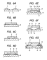
- Figs. 6A to 6G taken along the line VI-VI of Fig. 1A , are schematic cross-sectional views illustrating one example of the method for manufacturing a liquid discharge head of the present invention.
- a silicon-wafer-shaped substrate 15 shown in Fig. 6A has a crystal orientation ⁇ 100> plane.
- the ⁇ 100> plane is employed in the example; however, the present invention is not limited to this orientation.
- the intimate contact enhancement layer 7 is patterned in a predetermined shape on the substrate 15.
- the intimate contact enhancement layer 7 is made of a polyether amide resin. More specifically, the layer 7 may be made of HIMAL-1200 (product name) by Hitachi Chemical Co., Ltd.
- the intimate contact enhancement layer 7 has a thickness of 2 ⁇ m.
- a resin layer 16 composed of a positive photosensitive resin or the like on the substrate.
- the resin can be a polyketone-based resin or a methacrylate-based resin.
- the resin layer 16 has a height of 12 ⁇ m.
- a first mold 8 in the shape of said flow path and a second mold 17 for forming said cavity 4 are separately formed from the resin layer 16.
- the second mold 17 has the shape of a character corresponding to the shape of the cavity 4 to be formed.
- the layer 16 of the positive photosensitive resin is collectively subjected to proximity exposure to light over the entire surface of the wafer so that the first mold 8 can yield the same character shape and the second mold 17 can provide a different character shape for each of the chip units.
- the character shows the position of each chip unit in the wafer. This is made possible by editing the exposure mask.
- the subsequent development allows the mold to be formed.
- the mold is plural in number corresponding to the number of liquid discharge heads to be manufactured by cutting the wafer.
- a coating layer 18 which is made of a negative photosensitive resin such as a photosensitive epoxy resin and the like and serves as the flow path wall member, is provided on the substrate so as to cover the first mold 8 and the second mold 17.
- the coating layer 18 can be coated by spin coating or the like.
- the coating layer 18 is optically processed, i.e., exposed to light, developed, and the like, thereby forming a first opening 11a serving as a discharge port and a second opening 19 for removing the second mold to form the cavity.
- the first opening 11a is formed on the first mold and the second opening 19 is formed on the second mold.
- the second mold 17 is exposed by forming an outer side face 20 in the coating layer 18. The light exposure and development are performed so that flow path wall members are formed in plurality corresponding to the number of liquid discharge heads which are to be formed by being cut from the wafer.
- a supply port 13 is formed in the substrate 15, and the first mold and the second mold are collectively removed by dissolution, ultrasound, or the like.
- the flow path 14, the discharge port 11, and the flow path wall member 9 are formed.
- the character-shaped cavities 4 are also collectively formed together with the flow path.
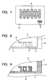
- Fig. 8 shows the cavities when viewed from above the substrate. The cavity 4 are opened on the outer side face 5 side of the flow path wall member 9 and on the side in which the discharge port 11 is provided by the second opening 19.
- the wafer-shaped substrate 15 is cut by dicing or the like to be divided into one or a predetermined number of flow path wall members as a unit, thereby allowing a liquid discharge head to be manufactured with a flow path wall member and the like provided on the substrate 12 as a chip unit.
- the liquid discharge head is placed on a supporting member 21 made of alumina or the like to join the substrate 12 and the supporting member 21 together by an adhesive or the like. Then, an end face 22 of the substrate 12 which is made by die cutting is sealed with a seal member 10.
- the sealing is performed by a sealing material such as a butadiene-based epoxy and the like to protect the end face against a mist or the like of discharged liquid such as ink mist and the like. More specifically, a product of the seal material may be NR 200C (product name) manufactured by Sanyu Rec Co., Ltd. In that process, the seal member 10 is injected by capillarity from the outer side face 5 of the flow path wall member 9 into the cavity 4.
- FIG. 9 is a top plan view of a history information display portion when viewed from above the substrate. As illustrated, if the seal member 10 allows the character to be transparent from the outer side face 5 to the inside of the flow path wall member 9, a black seal member 10 can be injected to further enhance the contrast, thereby ensuring greater ease in reading the history information.
Landscapes
- Engineering & Computer Science (AREA)
- Manufacturing & Machinery (AREA)
- Particle Formation And Scattering Control In Inkjet Printers (AREA)
Applications Claiming Priority (1)
| Application Number | Priority Date | Filing Date | Title |
|---|---|---|---|
| JP2009194455 | 2009-08-25 |
Publications (3)
| Publication Number | Publication Date |
|---|---|
| EP2289700A1 EP2289700A1 (en) | 2011-03-02 |
| EP2289700A8 EP2289700A8 (en) | 2011-04-27 |
| EP2289700B1 true EP2289700B1 (en) | 2013-07-03 |
Family
ID=43070447
Family Applications (1)
| Application Number | Title | Priority Date | Filing Date |
|---|---|---|---|
| EP10008808.7A Not-in-force EP2289700B1 (en) | 2009-08-25 | 2010-08-24 | Liquid discharge head and method for manufacturing the same |
Country Status (7)
| Country | Link |
|---|---|
| US (1) | US8342659B2 (enExample) |
| EP (1) | EP2289700B1 (enExample) |
| JP (1) | JP5679737B2 (enExample) |
| KR (1) | KR101331318B1 (enExample) |
| CN (1) | CN101992598B (enExample) |
| BR (1) | BRPI1003190B1 (enExample) |
| RU (1) | RU2427470C1 (enExample) |
Families Citing this family (9)
| Publication number | Priority date | Publication date | Assignee | Title |
|---|---|---|---|---|
| JP5393423B2 (ja) * | 2009-12-10 | 2014-01-22 | キヤノン株式会社 | インク吐出ヘッド及びその製造方法 |
| JP5791368B2 (ja) | 2011-05-20 | 2015-10-07 | キヤノン株式会社 | インクジェット記録ヘッドの製造方法 |
| JP6000715B2 (ja) | 2011-09-29 | 2016-10-05 | キヤノン株式会社 | 液体吐出ヘッドの製造方法 |
| JP5955082B2 (ja) | 2012-04-26 | 2016-07-20 | キヤノン株式会社 | 記録ヘッド及びインクジェット記録装置 |
| US10040290B2 (en) | 2016-01-08 | 2018-08-07 | Canon Kabushiki Kaisha | Liquid ejection head, liquid ejection apparatus, and method of supplying liquid |
| JP6929639B2 (ja) | 2016-01-08 | 2021-09-01 | キヤノン株式会社 | 液体吐出ヘッド、液体吐出装置及び液体の供給方法 |
| KR20250046352A (ko) | 2018-06-25 | 2025-04-02 | 오토테크 엔지니어링 에스.엘. | 차량의 본체 측면 구조 프레임 |
| JP2023159983A (ja) * | 2022-04-21 | 2023-11-02 | キヤノン株式会社 | 記録素子基板およびその製造方法 |
| JP2024049554A (ja) * | 2022-09-29 | 2024-04-10 | キヤノン株式会社 | 液体吐出ヘッドおよび記録装置 |
Family Cites Families (18)
| Publication number | Priority date | Publication date | Assignee | Title |
|---|---|---|---|---|
| US5235351A (en) * | 1984-03-31 | 1993-08-10 | Canon Kabushiki Kaisha | Liquid ejection recording head including a symbol indicating information used for changing the operation of the head |
| JPH0574748A (ja) | 1991-09-12 | 1993-03-26 | Hitachi Ltd | 来歴情報記録方式、及び半導体集積回路 |
| JP3459703B2 (ja) * | 1995-06-20 | 2003-10-27 | キヤノン株式会社 | インクジェットヘッドの製造方法、およびインクジェットヘッド |
| ATE475537T1 (de) * | 1998-08-31 | 2010-08-15 | Seiko Epson Corp | Druckvorrichtung und druckkopfeinheit |
| JP3928681B2 (ja) * | 1999-02-18 | 2007-06-13 | 富士ゼロックス株式会社 | 半導体装置およびその製造方法 |
| JP4731763B2 (ja) | 2001-09-12 | 2011-07-27 | キヤノン株式会社 | 液体噴射記録ヘッドおよびその製造方法 |
| EP1477316B1 (en) | 2002-02-19 | 2008-05-14 | Brother Kogyo Kabushiki Kaisha | Ink jet head and ink jet printer |
| US7171748B2 (en) * | 2002-08-30 | 2007-02-06 | Canon Kabushiki Kaisha | Method of manufacturing a liquid jet recording head |
| JP2005111976A (ja) * | 2003-09-18 | 2005-04-28 | Ricoh Co Ltd | 消耗部品、部品装着構造、及び画像形成装置 |
| JP2005181560A (ja) | 2003-12-18 | 2005-07-07 | Nippon Hoso Kyokai <Nhk> | 光導波路デバイス |
| JP4235820B2 (ja) * | 2004-05-07 | 2009-03-11 | ブラザー工業株式会社 | インクジェット記録ヘッド、ヘッドユニット及びインクジェット記録ヘッドの製造方法 |
| JP4194580B2 (ja) * | 2004-06-02 | 2008-12-10 | キヤノン株式会社 | ヘッド基板、記録ヘッド、ヘッドカートリッジ、及び記録装置 |
| JP2006082329A (ja) | 2004-09-15 | 2006-03-30 | Canon Inc | インクジェット記録ヘッドの製造方法 |
| JP2006351772A (ja) * | 2005-06-15 | 2006-12-28 | Fujifilm Holdings Corp | 半導体チップの識別情報記録方法及び撮像装置 |
| JP4341688B2 (ja) | 2006-04-12 | 2009-10-07 | セイコーエプソン株式会社 | 液体収容容器 |
| FR2906646B1 (fr) | 2006-10-03 | 2009-01-30 | Microcomposants De Haute Secur | Procede de marquage individuel de circuits integres et circuit integre marque selon ce procede. |
| US7571970B2 (en) * | 2007-07-13 | 2009-08-11 | Xerox Corporation | Self-aligned precision datums for array die placement |
| JP2009274266A (ja) | 2008-05-13 | 2009-11-26 | Canon Inc | 半導体チップ及び、インクジェット記録ヘッド |
-
2010
- 2010-08-06 US US12/851,704 patent/US8342659B2/en active Active
- 2010-08-17 KR KR1020100079246A patent/KR101331318B1/ko not_active Expired - Fee Related
- 2010-08-20 CN CN201010260865.3A patent/CN101992598B/zh active Active
- 2010-08-23 BR BRPI1003190-1A patent/BRPI1003190B1/pt not_active IP Right Cessation
- 2010-08-24 EP EP10008808.7A patent/EP2289700B1/en not_active Not-in-force
- 2010-08-24 RU RU2010135494/12A patent/RU2427470C1/ru not_active IP Right Cessation
- 2010-08-25 JP JP2010188487A patent/JP5679737B2/ja active Active
Also Published As
| Publication number | Publication date |
|---|---|
| BRPI1003190A2 (pt) | 2012-05-02 |
| RU2427470C1 (ru) | 2011-08-27 |
| CN101992598A (zh) | 2011-03-30 |
| US20110050828A1 (en) | 2011-03-03 |
| EP2289700A8 (en) | 2011-04-27 |
| KR20110021659A (ko) | 2011-03-04 |
| EP2289700A1 (en) | 2011-03-02 |
| CN101992598B (zh) | 2014-05-07 |
| US8342659B2 (en) | 2013-01-01 |
| JP5679737B2 (ja) | 2015-03-04 |
| BRPI1003190B1 (pt) | 2019-11-05 |
| JP2011068129A (ja) | 2011-04-07 |
| KR101331318B1 (ko) | 2013-11-20 |
Similar Documents
| Publication | Publication Date | Title |
|---|---|---|
| EP2289700B1 (en) | Liquid discharge head and method for manufacturing the same | |
| KR100816568B1 (ko) | 액체 토출 헤드 제조 방법 | |
| EP2878446B1 (en) | Method for manufacturing liquid discharge head | |
| JP2013003535A (ja) | 2次元コード付きラベル | |
| US20080309733A1 (en) | Liquid discharging head, producing method thereof, structure, and producing method thereof | |
| US8083423B2 (en) | Thermal indicators | |
| US8596759B2 (en) | Liquid ejection head and method of manufacturing the same | |
| JP2019188736A (ja) | インク容器及びインクジェット記録装置 | |
| US8408678B2 (en) | Liquid ejection head and method for producing the same | |
| US20190217617A1 (en) | Method of producing structure, protective substrate, and method of producing protective substrate | |
| JP3928681B2 (ja) | 半導体装置およびその製造方法 | |
| US8968584B2 (en) | Method for manufacturing liquid ejection head | |
| JP4999964B2 (ja) | 液体吐出ヘッドおよびその製造方法 | |
| JP2009274266A (ja) | 半導体チップ及び、インクジェット記録ヘッド | |
| KR101952199B1 (ko) | 마킹시스템 | |
| JP2007022022A (ja) | 感熱印刷媒体 | |
| JP4800684B2 (ja) | 配送伝票 | |
| JP2000318167A (ja) | インクジェット記録ヘッド及びその製造方法 | |
| JP5063390B2 (ja) | インクジェット記録ヘッドの製造方法 | |
| JP2007216631A (ja) | インクジェット記録ヘッド用基板及びそれを用いたインクジェット記録ヘッド |
Legal Events
| Date | Code | Title | Description |
|---|---|---|---|
| PUAI | Public reference made under article 153(3) epc to a published international application that has entered the european phase |
Free format text: ORIGINAL CODE: 0009012 |
|
| AK | Designated contracting states |
Kind code of ref document: A1 Designated state(s): AL AT BE BG CH CY CZ DE DK EE ES FI FR GB GR HR HU IE IS IT LI LT LU LV MC MK MT NL NO PL PT RO SE SI SK SM TR |
|
| AX | Request for extension of the european patent |
Extension state: BA ME RS |
|
| RIN1 | Information on inventor provided before grant (corrected) |
Inventor name: TAGAWA, YOSHINORI Inventor name: ASAI, KAZUHIRO Inventor name: FUJII, KENJI Inventor name: IMANAKA, YOSHIYUKI Inventor name: KUBO, KOUSUKE Inventor name: WATANABE, MAKOTO Inventor name: TAMARU, YUUJI |
|
| 17P | Request for examination filed |
Effective date: 20110902 |
|
| 17Q | First examination report despatched |
Effective date: 20120308 |
|
| GRAP | Despatch of communication of intention to grant a patent |
Free format text: ORIGINAL CODE: EPIDOSNIGR1 |
|
| GRAS | Grant fee paid |
Free format text: ORIGINAL CODE: EPIDOSNIGR3 |
|
| GRAA | (expected) grant |
Free format text: ORIGINAL CODE: 0009210 |
|
| AK | Designated contracting states |
Kind code of ref document: B1 Designated state(s): AL AT BE BG CH CY CZ DE DK EE ES FI FR GB GR HR HU IE IS IT LI LT LU LV MC MK MT NL NO PL PT RO SE SI SK SM TR |
|
| REG | Reference to a national code |
Ref country code: GB Ref legal event code: FG4D |
|
| REG | Reference to a national code |
Ref country code: CH Ref legal event code: EP Ref country code: AT Ref legal event code: REF Ref document number: 619485 Country of ref document: AT Kind code of ref document: T Effective date: 20130715 |
|
| REG | Reference to a national code |
Ref country code: IE Ref legal event code: FG4D |
|
| REG | Reference to a national code |
Ref country code: DE Ref legal event code: R096 Ref document number: 602010008128 Country of ref document: DE Effective date: 20130822 |
|
| PG25 | Lapsed in a contracting state [announced via postgrant information from national office to epo] |
Ref country code: SI Free format text: LAPSE BECAUSE OF FAILURE TO SUBMIT A TRANSLATION OF THE DESCRIPTION OR TO PAY THE FEE WITHIN THE PRESCRIBED TIME-LIMIT Effective date: 20130703 |
|
| REG | Reference to a national code |
Ref country code: AT Ref legal event code: MK05 Ref document number: 619485 Country of ref document: AT Kind code of ref document: T Effective date: 20130703 |
|
| REG | Reference to a national code |
Ref country code: NL Ref legal event code: VDEP Effective date: 20130703 |
|
| REG | Reference to a national code |
Ref country code: LT Ref legal event code: MG4D |
|
| PG25 | Lapsed in a contracting state [announced via postgrant information from national office to epo] |
Ref country code: SE Free format text: LAPSE BECAUSE OF FAILURE TO SUBMIT A TRANSLATION OF THE DESCRIPTION OR TO PAY THE FEE WITHIN THE PRESCRIBED TIME-LIMIT Effective date: 20130703 Ref country code: CY Free format text: LAPSE BECAUSE OF FAILURE TO SUBMIT A TRANSLATION OF THE DESCRIPTION OR TO PAY THE FEE WITHIN THE PRESCRIBED TIME-LIMIT Effective date: 20130710 Ref country code: LT Free format text: LAPSE BECAUSE OF FAILURE TO SUBMIT A TRANSLATION OF THE DESCRIPTION OR TO PAY THE FEE WITHIN THE PRESCRIBED TIME-LIMIT Effective date: 20130703 Ref country code: AT Free format text: LAPSE BECAUSE OF FAILURE TO SUBMIT A TRANSLATION OF THE DESCRIPTION OR TO PAY THE FEE WITHIN THE PRESCRIBED TIME-LIMIT Effective date: 20130703 Ref country code: BE Free format text: LAPSE BECAUSE OF FAILURE TO SUBMIT A TRANSLATION OF THE DESCRIPTION OR TO PAY THE FEE WITHIN THE PRESCRIBED TIME-LIMIT Effective date: 20130703 Ref country code: PT Free format text: LAPSE BECAUSE OF FAILURE TO SUBMIT A TRANSLATION OF THE DESCRIPTION OR TO PAY THE FEE WITHIN THE PRESCRIBED TIME-LIMIT Effective date: 20131104 Ref country code: HR Free format text: LAPSE BECAUSE OF FAILURE TO SUBMIT A TRANSLATION OF THE DESCRIPTION OR TO PAY THE FEE WITHIN THE PRESCRIBED TIME-LIMIT Effective date: 20130703 Ref country code: IS Free format text: LAPSE BECAUSE OF FAILURE TO SUBMIT A TRANSLATION OF THE DESCRIPTION OR TO PAY THE FEE WITHIN THE PRESCRIBED TIME-LIMIT Effective date: 20131103 Ref country code: NO Free format text: LAPSE BECAUSE OF FAILURE TO SUBMIT A TRANSLATION OF THE DESCRIPTION OR TO PAY THE FEE WITHIN THE PRESCRIBED TIME-LIMIT Effective date: 20131003 |
|
| PG25 | Lapsed in a contracting state [announced via postgrant information from national office to epo] |
Ref country code: PL Free format text: LAPSE BECAUSE OF FAILURE TO SUBMIT A TRANSLATION OF THE DESCRIPTION OR TO PAY THE FEE WITHIN THE PRESCRIBED TIME-LIMIT Effective date: 20130703 Ref country code: NL Free format text: LAPSE BECAUSE OF FAILURE TO SUBMIT A TRANSLATION OF THE DESCRIPTION OR TO PAY THE FEE WITHIN THE PRESCRIBED TIME-LIMIT Effective date: 20130703 Ref country code: ES Free format text: LAPSE BECAUSE OF FAILURE TO SUBMIT A TRANSLATION OF THE DESCRIPTION OR TO PAY THE FEE WITHIN THE PRESCRIBED TIME-LIMIT Effective date: 20131014 Ref country code: FI Free format text: LAPSE BECAUSE OF FAILURE TO SUBMIT A TRANSLATION OF THE DESCRIPTION OR TO PAY THE FEE WITHIN THE PRESCRIBED TIME-LIMIT Effective date: 20130703 Ref country code: GR Free format text: LAPSE BECAUSE OF FAILURE TO SUBMIT A TRANSLATION OF THE DESCRIPTION OR TO PAY THE FEE WITHIN THE PRESCRIBED TIME-LIMIT Effective date: 20131004 Ref country code: LV Free format text: LAPSE BECAUSE OF FAILURE TO SUBMIT A TRANSLATION OF THE DESCRIPTION OR TO PAY THE FEE WITHIN THE PRESCRIBED TIME-LIMIT Effective date: 20130703 |
|
| PG25 | Lapsed in a contracting state [announced via postgrant information from national office to epo] |
Ref country code: CY Free format text: LAPSE BECAUSE OF FAILURE TO SUBMIT A TRANSLATION OF THE DESCRIPTION OR TO PAY THE FEE WITHIN THE PRESCRIBED TIME-LIMIT Effective date: 20130703 |
|
| PG25 | Lapsed in a contracting state [announced via postgrant information from national office to epo] |
Ref country code: RO Free format text: LAPSE BECAUSE OF FAILURE TO SUBMIT A TRANSLATION OF THE DESCRIPTION OR TO PAY THE FEE WITHIN THE PRESCRIBED TIME-LIMIT Effective date: 20130703 Ref country code: DK Free format text: LAPSE BECAUSE OF FAILURE TO SUBMIT A TRANSLATION OF THE DESCRIPTION OR TO PAY THE FEE WITHIN THE PRESCRIBED TIME-LIMIT Effective date: 20130703 Ref country code: CZ Free format text: LAPSE BECAUSE OF FAILURE TO SUBMIT A TRANSLATION OF THE DESCRIPTION OR TO PAY THE FEE WITHIN THE PRESCRIBED TIME-LIMIT Effective date: 20130703 Ref country code: MC Free format text: LAPSE BECAUSE OF FAILURE TO SUBMIT A TRANSLATION OF THE DESCRIPTION OR TO PAY THE FEE WITHIN THE PRESCRIBED TIME-LIMIT Effective date: 20130703 Ref country code: SK Free format text: LAPSE BECAUSE OF FAILURE TO SUBMIT A TRANSLATION OF THE DESCRIPTION OR TO PAY THE FEE WITHIN THE PRESCRIBED TIME-LIMIT Effective date: 20130703 Ref country code: EE Free format text: LAPSE BECAUSE OF FAILURE TO SUBMIT A TRANSLATION OF THE DESCRIPTION OR TO PAY THE FEE WITHIN THE PRESCRIBED TIME-LIMIT Effective date: 20130703 |
|
| PLBE | No opposition filed within time limit |
Free format text: ORIGINAL CODE: 0009261 |
|
| STAA | Information on the status of an ep patent application or granted ep patent |
Free format text: STATUS: NO OPPOSITION FILED WITHIN TIME LIMIT |
|
| REG | Reference to a national code |
Ref country code: IE Ref legal event code: MM4A |
|
| REG | Reference to a national code |
Ref country code: FR Ref legal event code: ST Effective date: 20140430 |
|
| PG25 | Lapsed in a contracting state [announced via postgrant information from national office to epo] |
Ref country code: IT Free format text: LAPSE BECAUSE OF FAILURE TO SUBMIT A TRANSLATION OF THE DESCRIPTION OR TO PAY THE FEE WITHIN THE PRESCRIBED TIME-LIMIT Effective date: 20130703 |
|
| 26N | No opposition filed |
Effective date: 20140404 |
|
| REG | Reference to a national code |
Ref country code: DE Ref legal event code: R097 Ref document number: 602010008128 Country of ref document: DE Effective date: 20140404 |
|
| PG25 | Lapsed in a contracting state [announced via postgrant information from national office to epo] |
Ref country code: IE Free format text: LAPSE BECAUSE OF NON-PAYMENT OF DUE FEES Effective date: 20130824 |
|
| PG25 | Lapsed in a contracting state [announced via postgrant information from national office to epo] |
Ref country code: FR Free format text: LAPSE BECAUSE OF NON-PAYMENT OF DUE FEES Effective date: 20130903 |
|
| REG | Reference to a national code |
Ref country code: CH Ref legal event code: PL |
|
| PG25 | Lapsed in a contracting state [announced via postgrant information from national office to epo] |
Ref country code: LI Free format text: LAPSE BECAUSE OF NON-PAYMENT OF DUE FEES Effective date: 20140831 Ref country code: CH Free format text: LAPSE BECAUSE OF NON-PAYMENT OF DUE FEES Effective date: 20140831 |
|
| PG25 | Lapsed in a contracting state [announced via postgrant information from national office to epo] |
Ref country code: SM Free format text: LAPSE BECAUSE OF FAILURE TO SUBMIT A TRANSLATION OF THE DESCRIPTION OR TO PAY THE FEE WITHIN THE PRESCRIBED TIME-LIMIT Effective date: 20130703 |
|
| PG25 | Lapsed in a contracting state [announced via postgrant information from national office to epo] |
Ref country code: MT Free format text: LAPSE BECAUSE OF FAILURE TO SUBMIT A TRANSLATION OF THE DESCRIPTION OR TO PAY THE FEE WITHIN THE PRESCRIBED TIME-LIMIT Effective date: 20130703 Ref country code: TR Free format text: LAPSE BECAUSE OF FAILURE TO SUBMIT A TRANSLATION OF THE DESCRIPTION OR TO PAY THE FEE WITHIN THE PRESCRIBED TIME-LIMIT Effective date: 20130703 |
|
| PG25 | Lapsed in a contracting state [announced via postgrant information from national office to epo] |
Ref country code: MK Free format text: LAPSE BECAUSE OF FAILURE TO SUBMIT A TRANSLATION OF THE DESCRIPTION OR TO PAY THE FEE WITHIN THE PRESCRIBED TIME-LIMIT Effective date: 20130703 Ref country code: BG Free format text: LAPSE BECAUSE OF FAILURE TO SUBMIT A TRANSLATION OF THE DESCRIPTION OR TO PAY THE FEE WITHIN THE PRESCRIBED TIME-LIMIT Effective date: 20130703 Ref country code: LU Free format text: LAPSE BECAUSE OF NON-PAYMENT OF DUE FEES Effective date: 20130824 Ref country code: HU Free format text: LAPSE BECAUSE OF FAILURE TO SUBMIT A TRANSLATION OF THE DESCRIPTION OR TO PAY THE FEE WITHIN THE PRESCRIBED TIME-LIMIT; INVALID AB INITIO Effective date: 20100824 |
|
| PG25 | Lapsed in a contracting state [announced via postgrant information from national office to epo] |
Ref country code: AL Free format text: LAPSE BECAUSE OF FAILURE TO SUBMIT A TRANSLATION OF THE DESCRIPTION OR TO PAY THE FEE WITHIN THE PRESCRIBED TIME-LIMIT Effective date: 20130703 |
|
| PGFP | Annual fee paid to national office [announced via postgrant information from national office to epo] |
Ref country code: GB Payment date: 20190829 Year of fee payment: 10 |
|
| PGFP | Annual fee paid to national office [announced via postgrant information from national office to epo] |
Ref country code: DE Payment date: 20191031 Year of fee payment: 10 |
|
| REG | Reference to a national code |
Ref country code: DE Ref legal event code: R119 Ref document number: 602010008128 Country of ref document: DE |
|
| GBPC | Gb: european patent ceased through non-payment of renewal fee |
Effective date: 20200824 |
|
| PG25 | Lapsed in a contracting state [announced via postgrant information from national office to epo] |
Ref country code: DE Free format text: LAPSE BECAUSE OF NON-PAYMENT OF DUE FEES Effective date: 20210302 |
|
| PG25 | Lapsed in a contracting state [announced via postgrant information from national office to epo] |
Ref country code: GB Free format text: LAPSE BECAUSE OF NON-PAYMENT OF DUE FEES Effective date: 20200824 |