EP2254149A2 - SRAM mit vertikalen Transistoren mit einer Diffusionsschicht zur Verminderung von Leckströmen - Google Patents
SRAM mit vertikalen Transistoren mit einer Diffusionsschicht zur Verminderung von Leckströmen Download PDFInfo
- Publication number
- EP2254149A2 EP2254149A2 EP10005356A EP10005356A EP2254149A2 EP 2254149 A2 EP2254149 A2 EP 2254149A2 EP 10005356 A EP10005356 A EP 10005356A EP 10005356 A EP10005356 A EP 10005356A EP 2254149 A2 EP2254149 A2 EP 2254149A2
- Authority
- EP
- European Patent Office
- Prior art keywords
- diffusion layer
- transistor
- lower diffusion
- nmos
- layer
- Prior art date
- Legal status (The legal status is an assumption and is not a legal conclusion. Google has not performed a legal analysis and makes no representation as to the accuracy of the status listed.)
- Granted
Links
Images
















Classifications
-
- H—ELECTRICITY
- H10—SEMICONDUCTOR DEVICES; ELECTRIC SOLID-STATE DEVICES NOT OTHERWISE PROVIDED FOR
- H10B—ELECTRONIC MEMORY DEVICES
- H10B10/00—Static random access memory [SRAM] devices
-
- H—ELECTRICITY
- H10—SEMICONDUCTOR DEVICES; ELECTRIC SOLID-STATE DEVICES NOT OTHERWISE PROVIDED FOR
- H10D—INORGANIC ELECTRIC SEMICONDUCTOR DEVICES
- H10D62/00—Semiconductor bodies, or regions thereof, of devices having potential barriers
- H10D62/10—Shapes, relative sizes or dispositions of the regions of the semiconductor bodies; Shapes of the semiconductor bodies
- H10D62/17—Semiconductor regions connected to electrodes not carrying current to be rectified, amplified or switched, e.g. channel regions
- H10D62/351—Substrate regions of field-effect devices
- H10D62/357—Substrate regions of field-effect devices of FETs
- H10D62/364—Substrate regions of field-effect devices of FETs of IGFETs
- H10D62/371—Inactive supplementary semiconductor regions, e.g. for preventing punch-through, improving capacity effect or leakage current
-
- H—ELECTRICITY
- H10—SEMICONDUCTOR DEVICES; ELECTRIC SOLID-STATE DEVICES NOT OTHERWISE PROVIDED FOR
- H10B—ELECTRONIC MEMORY DEVICES
- H10B10/00—Static random access memory [SRAM] devices
- H10B10/12—Static random access memory [SRAM] devices comprising a MOSFET load element
-
- H—ELECTRICITY
- H10—SEMICONDUCTOR DEVICES; ELECTRIC SOLID-STATE DEVICES NOT OTHERWISE PROVIDED FOR
- H10B—ELECTRONIC MEMORY DEVICES
- H10B99/00—Subject matter not provided for in other groups of this subclass
-
- H—ELECTRICITY
- H10—SEMICONDUCTOR DEVICES; ELECTRIC SOLID-STATE DEVICES NOT OTHERWISE PROVIDED FOR
- H10D—INORGANIC ELECTRIC SEMICONDUCTOR DEVICES
- H10D30/00—Field-effect transistors [FET]
- H10D30/01—Manufacture or treatment
- H10D30/021—Manufacture or treatment of FETs having insulated gates [IGFET]
- H10D30/025—Manufacture or treatment of FETs having insulated gates [IGFET] of vertical IGFETs
-
- H—ELECTRICITY
- H10—SEMICONDUCTOR DEVICES; ELECTRIC SOLID-STATE DEVICES NOT OTHERWISE PROVIDED FOR
- H10D—INORGANIC ELECTRIC SEMICONDUCTOR DEVICES
- H10D30/00—Field-effect transistors [FET]
- H10D30/60—Insulated-gate field-effect transistors [IGFET]
- H10D30/63—Vertical IGFETs
-
- H—ELECTRICITY
- H10—SEMICONDUCTOR DEVICES; ELECTRIC SOLID-STATE DEVICES NOT OTHERWISE PROVIDED FOR
- H10D—INORGANIC ELECTRIC SEMICONDUCTOR DEVICES
- H10D84/00—Integrated devices formed in or on semiconductor substrates that comprise only semiconducting layers, e.g. on Si wafers or on GaAs-on-Si wafers
- H10D84/80—Integrated devices formed in or on semiconductor substrates that comprise only semiconducting layers, e.g. on Si wafers or on GaAs-on-Si wafers characterised by the integration of at least one component covered by groups H10D12/00 or H10D30/00, e.g. integration of IGFETs
- H10D84/82—Integrated devices formed in or on semiconductor substrates that comprise only semiconducting layers, e.g. on Si wafers or on GaAs-on-Si wafers characterised by the integration of at least one component covered by groups H10D12/00 or H10D30/00, e.g. integration of IGFETs of only field-effect components
- H10D84/83—Integrated devices formed in or on semiconductor substrates that comprise only semiconducting layers, e.g. on Si wafers or on GaAs-on-Si wafers characterised by the integration of at least one component covered by groups H10D12/00 or H10D30/00, e.g. integration of IGFETs of only field-effect components of only insulated-gate FETs [IGFET]
- H10D84/834—Integrated devices formed in or on semiconductor substrates that comprise only semiconducting layers, e.g. on Si wafers or on GaAs-on-Si wafers characterised by the integration of at least one component covered by groups H10D12/00 or H10D30/00, e.g. integration of IGFETs of only field-effect components of only insulated-gate FETs [IGFET] comprising FinFETs
Definitions
- the present application relates to a semiconductor memory device, and more particularly to a semiconductor memory device composed of Static Random Access Memory (“SRAM").
- SRAM Static Random Access Memory
- a Surrounding Gate Transistor that is a vertical gate transistor is disclosed, having a columnar semiconductor formed on the surface of a semiconductor substrate and a gate formed on the side wall thereof so as to surround the columnar semiconductor layer (for example, see Unexamined Japanese Patent Application KOKAI Publication No. H2-188966 ).
- SGT Surrounding Gate Transistor
- the drain, gate and source are arranged in a vertical direction making it possible to greatly reduce the occupied surface area in comparison to traditional planar transistors.
- LSI large-scale integrated circuit
- SRAM composed in combination with the SGTs as the cache memory thereof.
- there has been extremely strong demand to increase the capacity of SRAM mounted on LSI so it is essential that SRAM having a small cell surface area be attained even when using SGTs.
- FIG. 25A shows an illustrative planar view of a CMOS-type 6T-SRAM containing six transistors designed using SGTs, as exhibited in the embodiment of Unexamined Japanese Patent Application KOKAI Publication No. H7-99311
- FIG. 25B shows a cross-sectional view thereof.
- Bit wires 801a and 801b are formed of an N+ diffusion layer
- ground potential wiring GND is formed of an N+ diffusion layer 802
- power source potential wiring Vcc is formed of a P+ diffusion layer 803.
- columnar silicon layers are formed constructing access transistors 810a and 810b in order to access memory cells, driver transistors 811a and 811b in order to drive the memory cells, and load transistors 812a and 812b in order to supply electrical charge to the memory cells.
- Gates 804a, 804b, 804c and 804d are formed to surround these columnar silicon layers.
- Memory nodes comprise wiring layers 807a and 807b.
- the various transistors constructing the SRAM have the source, gate and drain formed in a vertical direction on the columnar silicon layers, so it is possible to design small SRAM cells.
- the above-described SRAM cell has the following problems.
- the SRAM of Unexamined Japanese Patent Application KOKAI Publication No. H7-99311 when the power source potential wiring 803 and the ground potential wiring 802 formed inside the SRAM cell array are formed with the minimum dimensions, it is possible to attain a small cell surface area.
- the above-described power source potential wiring 803 and ground potential wiring 802 are formed of a P+ diffusion layer and an N+ diffusion layer, respectively. Therefore, when these are formed with the minimum dimensions, the SRAM has an extremely high resistance, making stable operation of the SRAM impossible.
- the dimensions of the power source potential wiring 803 and the ground potential wiring 802 are enlarged in order to attain stable operation of the SRAM, the SRAM cell surface area increases.
- the semiconductor memory device of the present application is a semiconductor memory device characterized by comprising multiple static memory cells in each of which a plurality of, approximately six, MOS transistors are arranged on a substrate, wherein each of the six MOS transistors comprises a lower diffusion layer formed on a surface of the substrate, a columnar semiconductor layer formed on the lower diffusion layer, an upper diffusion layer formed on the columnar semiconductor layer, a gate insulating film formed on the side wall of the columnar semiconductor layer to surround the columnar semiconductor layer, and a gate electrode formed on the gate insulating film to surround the gate insulating film; wherein the lower diffusion layer, columnar semiconductor layer, and upper diffusion layer are arranged on the substrate in layers in the vertical direction, one of the lower and upper diffusion layers serving as a source diffusion layer and the other serving as a drain diffusion layer; wherein the six MOS transistors serve as first and second NMOS access transistors for accessing the memory, first and second NMOS driver transistors for driving a memory node in order to retain data
- the semiconductor memory device is characterized by further comprising a first NMOS driver gate wiring extending from the first gate electrode of the first NMOS driver transistor and a first PMOS load gate wiring extending from the second gate electrode of the first PMOS load transistor which are connected by a common contacs, and a second NMOS driver gate wiring extending from the third gate electrode of the second NMOS driver transistor and a second PMOS load gate wiring extending from the fourth gate electrode of the second PMOS load transistor which are connected by a common contact.
- the circumference of the side wall of the columnar semiconductor layer constructing the first NMOS driver transistor has a value equal to or greater than the circumference of the side wall of the columnar semiconductor layer constructing the first NMOS access transistor
- the circumference of the side wall of the columnar semiconductor layer constructing the second NMOS driver transistor has a value equal to or greater than the circumference of the side wall of the columnar semiconductor layer constructing the second NMOS access transistor
- the circumference of the side wall of the columnar semiconductor layer constructing the first PMOS load transistor has a value equal to or less than the circumference of the side wall of the columnar semiconductor layer constructing the first NMOS access transistor.
- the circumference of the side wall of the columnar semiconductor layer constructing the second PMOS load transistor has a value equal to or less than the circumference of the side wall of the columnar semiconductor layer constructing the second NMOS access transistor.
- At least one of the contact formed on the first NMOS access gate wiring extending from the fifth gate electrode of the first NMOS access transistor and the contact formed on the second NMOS access gate wiring extending from the sixth gate electrode of the second NMOS access transistor is shared with the contact formed on the adjacent gate wiring extending from the gate electrode of the first or second NMOS access transistor of the adjacent memory cell.
- the columnar semiconductor layers constructing the MOS transistors are arranged in a hexagonal lattice shape.
- the first NMOS driver gate wiring extending from the first gate electrode of the first NMOS driver transistor and the first PMOS load gate wiring extending from the second gate electrode of the first PMOS load transistor are connected by a common contact with the lower diffusion layers serving as the second memory node; and the second NMOS driver gate wiring extending from the third gate electrode of the second NMOS driver transistor and the second PMOS load gate wiring extending from the fourth gate electrode of the second PMOS load transistor are connected by a common contact with the lower diffusion layers serving as the first memory node.
- the contacts formed on the gate wirings extending from the gate electrodes of the first and second NMOS access transistors are shared.
- the contacts formed on the columnar semiconductor and the other contacts in the semiconductor device are formed through different lithographic or etching processes.
- FIGS. 2 , 5A , 6A , 7A , 8A , 9A , 10A , 11A , 12A , 13A , 14A , 15A , 16A , 17 to 23 , and 25A are planar views in which some part is hatched for distinguishing regions.
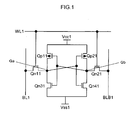
- FIG. 1 shows an equivalent circuit of a CMOS-type 6T-SRAM memory cell of Embodiment 1 of the present application.
- reference numbers BL1 and BLB1 indicate bit lines
- a reference number WL1 indicates a word line
- a reference number Vcc1 indicates a power source potential wire
- a reference number Vss1 indicates a ground potential wire
- reference numbers Qn11 and Qn21 indicate access transistors for accessing the memory cell
- reference numbers Qn31 and Qn41 indicate driver transistors for driving the memory cell
- reference numbers Qp11 and Qp21 indicate load transistors for supplying electric charge to the memory cell
- reference numbers Qa and Qb indicate memory nodes for storing data.
- the read operation in which data "L” is stored in the memory node Qa and data "H” is stored in the memory node Qb is described as an example of the operation of the memory cell in FIG. 1 .
- the bit lines BL1 and BLB1 are precharged to an "H” electric potential in the read-out operation. After precharging to these lines is completed, the word line WL1 goes to "H” and then, the readout of the data is initiated. At this time, the access transistors Qn11 and Qn21 turn on, and the driver transistor Qn31 turns on because the memory node Qb has a potential value close to the "H” electric potential.
- the electric potential of the bit line BL1 which is at "H” is discharged from the access transistor Qn11 via the memory node Qa and the driver transistors Qn31 and the electric potential of the bit line BL1 approaches an "L” electric potential.
- the driver transistor Qn41 is off because the memory node Qa has a potential value close to the "L” electric potential. Therefore, the electric potential of the bit line BLB1 is not discharged and conversely supplied from the load transistors Qp21 , so the potential of the bit line BLB1 remains close to the "H” electric potential.
- FIG. 2 shows a layout diagram for an SRAM memory cell of the first embodiment of the present application.
- the unit cell UC shown in FIG. 2 is repeatedly positioned in the SRAM cell array.
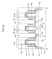
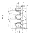
- FIGS. 3A , 3B , 3C and 3D show the cross-sectional structure along lines A-A', B-B', C-C' and D-D', respectively, in the layout diagram of FIG. 2 .
- a P-well which is a first well 1a
- the lower diffusion layer on the surface of the substrate is separated by an isolation layer 2 .
- the first memory node Qa comprising the lower diffusion layers in the surface region of the substrate is composed of a first N+ lower diffusion layer 3a, a second N+ lower diffusion layer 5a , and a third P+ lower diffusion layer 4a (also simply termed the lower diffusion layers, hereafter).
- the mutually adjacent N+ lower diffusion layers and P+ lower diffusion layer are connected by a silicide layer 13a formed on the substrate surface.
- a second memory node Qb comprising the lower diffusion layers in the surface region of the substrate is composed of a fourth N+ lower diffusion layer 3b, a fifth N+ lower diffusion layer 5b , and a sixth P+ lower diffusion layer 4b formed on the bottom of the access transistor Qn21 (also simply termed the lower diffusion layers, hereafter). And, the mutually adjacent N+ lower diffusion layers and P+ lower diffusion layer are connected by a silicide layer 13b formed on the surface of each of the diffusion layers.
- First and second anti-leak N+ diffusion layers 1b , 1c are formed at the bottoms of the P+ lower diffusion layers, which have the same conductive type as the P-well that is the first well 1a , in order to control leakage to the substrate.
- the first and second anti-leak N+ diffusion layers 1b , 1c are each separated by an isolation layer 2.
- Access transistors Qn11 and Qn21 are formed of NMOS and they are access transistors for accessing a memory cell.
- Driver transistors Qn31 and Qn41 are NMOS and they are driver transistors for driving memory cells.
- Load transistors Qp11 and Qp21 are PMOS and they are load transistors for supplying electric charge to memory cells.
- the single unit cell UC is provided with transistors arranged in three rows and two columns on the substrate. In the first column, the access transistor Qn11 , the load transistor Qp11 and the driver transistor Qn31 are arranged in order from the top of the diagram.
- the diffusion layers 3a, 4a and 5a arranged in the lower layers of transistors Qn11, Qp11 and Qn31 serve as the first memory node Qa .
- the driver transistor Qn41 the load transistor Qp21 and the access transistor Qn21 are arranged in order from the top of the diagram.
- the lower diffusion layers 3b, 4b and 5b arranged in the lower layer of transistors Qn41 , Qp21 and Qn21 serve as the second memory node Qb .
- the SRAM cell array according to this embodiment preferably contains unit cells UC, which are respectively provided with these six transistors, arranged continuously in the up and down direction in the drawing.
- a contact 10a formed on the lower diffusion layers on the substrate that are the first memory node Qa is connected to a contact 11b formed on the gate wiring extending from the gate electrodes of the load transistor Qp21 and the driver transistors Qn41 through node connection wiring Na1 . Furthermore, a contact 10b formed on the lower diffusion layers on the substrate that are the second memory node Qb is connected to a contact 11a formed on the gate wiring extending from the gate electrodes of the load transistor Qp11 and the driver transistor Qn31 through node connection wiring Nb1 .
- a contact 6a formed on top of the access transistor Qn11 is connected to the bit line BL1
- a contact 6b formed on top of the access transistor Qn21 is connected to the bit line BLB1 .
- a contact 7a formed on gate wiring extending from the gate electrode of the access transistor Qn11 and a contact 7b formed on gate wiring extending from the gate electrode of the access transistor Qn21 are connected to the word line WL1 .
- Contacts 8a , 8b formed on top of the driver transistors Qn31 , Qn41 are respectively connected to wiring layers Vss1a , Vss1b that are at ground potentials, and contacts 9a, 9b formed on top of the load transistors Qp11 , Qp21 are connected to the wiring Vcc1 that is at the power source potential.
- the wiring of the word lines, the wiring of the bit lines, the power source potential wiring and the ground potential wiring are preferably connected in a layer above the node connection wiring that is the wiring within each memory cell in order to be common with the wirings of other memory cells.
- the node connection wiring Na1 , Nb1 and the ground potential wiring Vss1a , Vss1b are wired in a layer below the bit lines BL1, BLB1 and below the power source potential wiring Vcc1 , in which the word line WL1 is wired in a layer above the bit lines BL1, BLB1 and the power source potential wiring Vcc1 .
- FIG. 2 shows N+ doping regions 24a, 24b and a P+ doping region 25.
- the pattern forming the N+ doping regions 24a, 24b and the P+ doping region 25 is formed of simple lines and spaces. Therefore, discrepancies in dimension or positioning have little effect, and it is possible to minimize the margin of dimensions near the boundaries of the N+ doping regions and the P+ doping region. As described in terms of the drawing, this arrangement is effective at reducing the length of the SRAM cell in the vertical direction (the length in the direction of connecting each SRAM cell).
- the memory nodes and gate wiring shown in the layout of FIG. 2 are formed in only a rectangular shape in this embodiment. Therefore, it is easy to correct the pattern shape through OPC (Optical Proximity Correction), and this layout is suitable for realizing a small SRAM cell surface area.
- OPC Optical Proximity Correction
- the source and drain of each transistor constructing the SRAM are defined as follows.
- the driver transistors Qn31 , Qn41 the upper diffusion layer formed on top of the columnar semiconductor layer connected to the ground voltage is defined as the source diffusion layer, and the lower diffusion layer formed below the columnar semiconductor layer is defined as the drain diffusion layer.
- the load transistors Qp11 , Qp21 the upper diffusion layer formed on top of the columnar semiconductor layer connected to the power source voltage is defined as the source diffusion layer, and the lower diffusion layer formed below the columnar semiconductor layer is defined as the drain diffusion layer.
- the upper diffusion layer formed on top of the columnar semiconductor layer and the lower diffusion layer formed below the columnar semiconductor layer are both source or drain depending on the operating state, but for convenience the upper diffusion layer formed on top of the columnar semiconductor layer is defined as the source diffusion layer and the lower diffusion layer formed below the columnar semiconductor layer is defined as the drain diffusion layer.
- a P-well that is the first well 1a is formed in the surface region of the substrate and the lower diffusion layers in the surface region of the substrate are separated by the isolation layer 2 .
- An N+ drain diffusion layer 3a is formed through conventional doping methods or the like in the first memory node Qa comprising the lower diffusion layers on the substrate, and a fifth N+ drain diffusion layer 5b is formed through conventional doping methods or the like in the second memory node Qb comprising the lower diffusion layers on the substrate.
- silicide layers 13a , 13b are formed on the surface of the N+ drain diffusion layers 3a, 5b .
- a columnar silicon layer 21a constructing the access transistor Qn11 is formed on top of the N+ drain diffusion layer 3a, and a columnar silicon layer 22b constructing the driver transistor Qn41 is formed on the N+ drain diffusion layer 5b .
- a gate insulating film 17 and a gate electrode 18 are formed surrounding these columnar silicon layers.
- An N+ source diffusion layer 14 is formed through conventional doping methods or the like on top of the columnar silicon layer, and a silicide layer 15 is formed on the source diffusion layer.
- the contact 6a formed on top of the access transistor Qn11 is connected to the bit line BL1
- the contact 7a formed on top of the gate wiring 18a extending from the gate electrode 18 of the access transistor Qn11 is connected to the word line WL1
- the contact 8b formed on top of the driver transistor Qn41 is connected to the ground potential wiring Vss1 .
- the P-well that is the first well 1a is formed in the surface region of the substrate and the lower diffusion layers on the substrate are separated by the isolation layer 2.
- the N+ drain diffusion layer 3a is formed through conventional doping methods or the like in the first memory node Qa comprising the lower diffusion layers on the substrate
- the N+ drain diffusion layer 5b is formed through conventional doping methods or the like in the second memory node Qb comprising the lower diffusion layers on the substrate.
- silicide layers 13a , 13b are formed on the surface of the N+ drain diffusion layers 3a, 5b .
- the contact 10a formed on the drain diffusion layer 3a is formed on the boundary area of the N+ drain diffusion layer 3a and the P+ drain diffusion layer 4a.
- the contact 10a is connected via the memory node connection wiring Na1 to the contact 11b formed on the gate wiring 18b extending from the gate electrodes of the driver transistor Qn41 and the load transistor Qp21 .
- the P-well that is the first well 1a is formed in the surface region of the substrate and the lower diffusion layers on the substrate are separated by the isolation layer 2.
- the P+ drain diffusion layer 4a is formed through conventional doping methods or the like in the first memory node Qa comprising the lower diffusion layers on the substrate
- an P+ drain diffusion layer 4b is formed through conventional doping methods or the like in the second memory node Qb comprising the lower diffusion layers on the substrate.
- silicide layers 13a , 13b are formed on the surface of the P+ drain diffusion layers 4a, 4b.
- a first anti-leak N+ diffusion layer 1b having a conductive type differing from the first well 1a is formed at the bottom of the P+ lower diffusion layer 4a , which has the same conductive type as the first well 1a , in order to control leakage to the substrate.
- a second anti-leak N+ diffusion layer 1c having a conductive type differing from the first well 1a is formed at the bottom of the P+ diffusion layer 4b, which has the same conductive type as the first well 1a, in order to control leakage to the substrate.
- a columnar silicon layer 23a constructing the load transistor Qp11 is formed on the P+ drain diffusion layer 4a
- a columnar silicon layer 23b constructing the load transistor Qp21 is formed on the P+ drain diffusion layer 4b.
- the gate insulating film 17 and the gate electrode 18 are formed surrounding each of these columnar silicon layers.
- a P+ source diffusion layer 16 is formed through conventional doping methods or the like on top of the columnar silicon layer, and a silicide layer 15 is formed on the surface of the source diffusion layer 16.
- Contacts 9a, 9b formed on top of the load transistors Qp11 , Qp21 are both connected to the power source potential wiring Vcc1 via the wiring layer.
- the P-well that is the first well 1a is formed in the surface region of the substrate and the lower diffusion layers on the substrate are separated by the isolation layer 2.
- the N+ drain diffusion layers 3a, 5a and the P+ drain diffusion layer 4a are formed through conventional doping methods or the like in the first memory node Qa comprising the lower diffusion layers on the substrate.
- the silicide layer 13a is formed on the surface of the drain diffusion layer, and the N+ drain diffusion layers 3a, 5a and the P+ drain diffusion layer 4a are directly connected through the silicide layer 13a .
- a first anti-leak diffusion layer 1b having a conductive type differing from the first well 1a is formed at the bottom of the P+ diffusion layer 4a, which is of the same conductive type as the first well 1a , in order to control leakage to the substrate.
- a columnar silicon layer 21a constructing the access transistor Qn11 is formed on top of the N+ drain diffusion layer 3a
- a columnar silicon layer 22a constructing the driver transistor Qn31 is formed on the N+ drain diffusion layer 5a
- a columnar silicon layer 23a constructing the load transistor Qn1 is formed on top of the P+ drain diffusion layer 4a.
- the N+ drain diffusion layer 3a, the P+ drain diffusion layer 4a and the N+ drain diffusion layer 5a are directly connected by the silicide layer 13a formed on the surface region of the various diffusion layers.
- the gate insulating film 17 and the gate electrode 18 are formed on each of the columnar silicon layers.
- the source diffusion layers are formed through conventional doping methods or the like on top of the respective columnar silicon layers, and the silicide layer 15 is formed on the source of the diffusion layers.
- the contact 6a formed on the access transistor Qn11 is operably connected to the bit line BL1
- the contact 8a formed on the diver transistor Qn31 is operably connected to the ground potential wiring Vss1a
- the contact 9a formed on the load transistor Qp11 is operably connected to the power source potential wiring Vcc1 .
- the gate electrodes of the driver transistor Qn31 and the load transistor Qp11 are connected to the common contact 11a on the gate wiring 18c extending from each of the gate electrodes.
- the contact 11a is connected to the contact 10b formed on the drain diffusion layer in the memory node 2b via the memory node connection wiring Nb1 .
- the contact 10a formed on the boundary area of the drain diffusion layers 3a and 4a are connected to the contact 11b formed on the gate wiring 18d extending from the gate electrodes of the driver transistor Qn41 and the load transistor Qp21 via the memory node connection wiring Na1 .
- the drain diffusion layers of the access transistor, driver transistor and load transistor are common and serve as the memory node of the SRAM through the N+ drain diffusion layers and the P+ drain diffusion layer formed on surface of the substrate being directly connected by a silicide layer formed on the surface of the diffusion layers. Consequently, an isolation layer to separate the N+ source drain diffusion layer and the P+ source drain diffusion layer needed in a regular planar-type transistor is unnecessary, and an isolation layer to separate only the two memory nodes of the SRAM is sufficient, making it possible to attain an extremely small SRAM cell surface area.
- first and second anti-leak diffusion layers 1b , 1c having a conductive type differing from the first well 1a are formed at the bottoms of the drain diffusion layers having the same conductive type as the first well 1a to control leakage to the substrate.
- first well 1a is the N-well and first and second anti-leak P+ diffusion layers 1b , 1c are formed at the bottoms of the N+ lower diffusion layers, respectively.
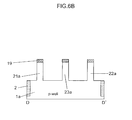
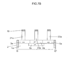
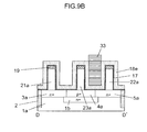
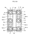
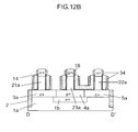
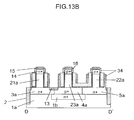
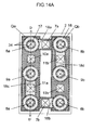
- FIGS. 5A through 16B A is a planar view and B is a cross-sectional view along the line D-D'.
- a mask 19 of silicon nitride film or the like is formed on the substrate.
- a columnar silicon layer 21a-23a, 21b-23b pattern is formed through lithography, and the columnar silicon layers 21a-23a, 21b-23b are formed through etching.
- the P-well which is the first well 1a , is formed in the SRAM cell array through conventional doping methods or the like.
- an isolation layer 2 is formed.
- the isolation layer 2 is formed by the method comprising the first step of etching a trench pattern, the step of forming a oxide film through embedding silica or the like in the trench with coating and CVD method, and the step of removing the excess oxide film on the substrate through dry etching or wet etching.
- the pattern of the diffusion layers that serve as the first memory node Qa and the second memory node Qb are formed on the substrate.
- dopants are introduced through conventional ion doping methods or the like in the N+ doping regions 24a and 24b and the P+ doping region 25 to form the drain diffusion layers (3a, 4a and 5a ) below the columnar silicon layers on the substrate.
- a first anti-leak N+ diffusion layer 1b is formed at the bottom of the P+ diffusion layer 4a, which has the same conductive type as the P-well that is the first well 1a , in order to control leakage to the substrate.
- the first anti-leak N+ diffusion layer 1b can be formed through conventional doping methods or the like with the mask of the P+ doping region 25.
- the first anti-leak N+ diffusion layer 1b is separated from that of the memory nodes by the isolation layer.
- the gate insulating film 17 and the gate conductor film 18e are formed.
- the gate insulating film 17 is formed of an oxide film and a High-k film.
- the gate conductor film is formed of polysilicon or a metal film.
- a gate wiring pattern is formed through lithography, using resist 33 and the like.
- the gate insulating film 17 and the gate conductive film 18e are etched and removed, with the resist 33 as a mask. Through these steps, the gate wiring 18a-18d and the gate electrode 18 are formed. Then the mask on the pillars is removed.
- an insulating film of silicon nitride or the like is formed and then etched back to form a structure in which the side walls of the columnar silicon layers and the side walls of the gate electrodes are covered by the insulating film 34 of silicon nitride or the like.
- dopants are respectively introduced through conventional ion doping methods or the like into the N+ doping regions and the P+ doping region to form source diffusion layers 14, 16 on top of the columnar silicon layers.
- metal such as Co or Ni is sputtered on the substrate and the sputtered substrate is heat-treated to selectively silicidize the source drain diffusion layers and form silicide layers 13a , 13b on the surface of the drain diffusion layers and a silicide layer 15 on the surface of the source diffusion layers on the columnar silicon layers.
- the insulating film 34 formed of silicon nitride or the like covering the side wall of the gate electrodes and columnar silicon layers.
- contacts 6a-11a , 6b-11b are formed after forming a silicon oxide film, which is an interlayer film.
- the contacts on the pillars are formed through a first lithography and etching step, and then, as shown in FIGS. 16A and 16B , the other contacts 7a, 10a , 11a , 7b, 10b, 11b are formed through a second lithography and etching step. Therefore, it is possible to reduce the minimum intervals between the contacts on the pillars and the other contacts and reduce the SRAM cell surface area.
- FIG. 17 shows an illustrative SRAM cell layout for this embodiment.
- the transistors arranged in one column of the unit cell UC in FIG. 17 in the SRAM cell array have the same positioning arrangement as the transistors arranged in the second column of the memory cells adjacent to the unit cell UC on the top side and the bottom side.
- the transistors arranged in the second column of the unit cell UC have the same positioning arrangement as the transistors arranged in the first column of the memory cells adjacent to the unit cell UC on the top side and the bottom side. That is to say, on the top side of the transistors Qn12 , Qp12 and Qn32 arranged in the first column of the unit cell UC in FIG.
- the same transistors as transistors Qn42 , Qp22 and Qn22 arranged in the second column are arranged, in order from the top. Accordingly, an access transistor is arranged adjacent to the top side of the access transistor Qn12 in the drawing, and an access transistor is arranged adjacent to the bottom side of the access transistor Qn22 in the drawing.
- the gate wiring extending from the gate electrode of the access transistor Qn12 is connected to the gate electrode of the access transistor of the memory cell adjacent on the top side in the drawing, so it possible to share the contacts 107a , 107b to the word line WL2 on that gate wiring.
- the contacts 7a, 7b to the word line WL1 were formed in the area between the first memory node and the second memory node, but in this embodiment, they are positioned on the boundary between upper and lower SRAM cells, so it is possible to reduce the space between memory nodes. In terms of the drawing, it is possible to reduce the length of the SRAM cell in the horizontal direction.
- the above-described sharing of contacts among gate electrodes in the access transistors can be applied to the transistors arranged as in Embodiment 1. For example, the gate wiring from the gate electrode of the access transistor Qn11 in FIG.
- the word line wiring, the bit line wiring, the power source potential wiring and the ground potential wiring are preferably positioned on the layer above the node connection wiring which is the wiring within each memory cell, and thus are shared with the wiring of other memory cells.
- the node connection wiring Na2 , Nb2 is wired in the lower layer
- the word line WL2 is wired in the middle layer
- the bit line wiring BL2, BLB2 the power source potential wiring Vcc2 and the ground potential wiring Vss2a , Vss2b are wired in the upper layer so that these wirings may avoid making any unsafe contact.
- the subsequent arrangement is the same as that of embodiment 1, so the arrangement's description will be omitted.
- FIG. 18 shows an illustrative SRAM layout for this embodiment.
- the difference from embodiment 2 is in a preferred shape of the columnar silicon layer that forms the driver transistor.
- the drain current of the driver transistors is generally set larger than the drain current of the access transistors in order to secure an operating margin during normal readout.
- the drain current can be increased by making the diffusion layer width of the driver transistor larger than the diffusion layer width of the access transistor.
- the shape of the columnar silicon layer may be in an elliptical or rectangular shape in order to lengthen the circumference of the columnar silicon layer.
- the circumference of the side wall of the columnar silicon layer forming the load transistor may be less than the circumference of the side wall of the columnar silicon layer forming the access transistor by enlarging the diameter of the access transistor and increasing the drain current value of the access transistor in order to increase operating speed, or by reducing the diameter of the load transistor and making the drain current of the load transistor relatively lower than the other transistors in order to improve write margins. In this manner, it is possible to adjust the properties of the various types of SRAM by changing the respective shapes of the access transistor, the driver transistor and the load transistor.
- the word line wiring, the bit line wiring, the power source potential wiring and the ground potential wiring are preferably positioned on the layer above the node connection wiring, which is the wiring within each memory cell, so as to be shared with the wiring of other memory cells.
- the same arrangement as in above-described embodiment 2 can be attained.
- the subsequent arrangement is the same as that of embodiment 2, so the arrangement's description will be omitted.
- IG. 19 shows an illustrative SRAM cell layout for this embodiment.
- This embodiment differs from embodiment 2 in that the gate wiring and the diffusion layers, which are the memory nodes, on the substrate are connected by common contacts formed over both the gate wiring and the diffusion layers in this embodiment.
- the diffusion layers on the substrate that are the memory node Qa4 and the gate wiring extending from the gate electrodes of the driver transistor Qn44 and the load transistor Qp24 are connected through a common contact 310a formed over both the diffusion layers and the gate wiring.
- the diffusion layers in the srface region of the substrate that are the memory node Qb4 and the gate wiring extending from the gate electrodes of the driver transistor Qn34 and the load transistor Qp14 are connected through a common contact 310b formed over both the diffusion layers and the gate wiring.
- the word line wiring, the bit line wiring, the power source potential wiring and the ground potential wiring are preferably positioned on the layer above the node connection wiring, which is the wiring within each memory cell, that is to say, they are positioned on a layer above the contact 310a and the contact 310b, so as to be shared with the wiring of other memory cells.
- the arrangement other than this point is the same as that of embodiment 2, so the arrangement's description will be omitted.
- FIG. 20 shows an illustrative SRAM cell layout for this embodiment.
- This embodiment differs from Embodiment 2 in that the positioning of the driver transistor and the load transistor are switched.
- the positioning of the driver transistor and the load transistor are switched, there is only one boundary between the P+ doping regions 425a , 425b and the N+ doping region that traverse the diffusion layers on the substrate that are the memory node. Therefore, there is only one place near the boundary of the N+ doping region and the P+ doping regions where the overlapping margin must be secured, and it is possible to reduce the length of the SRAM cell in the vertical direction.
- the N+ doping region and the P+ doping regions are not simple line and space, as the P+ doping regions 425a , 425b are a rectangular grooved pattern, while the N+ doping region is a pattern that is the reverse of the P+ doping regions 425a, 425b.
- the positioning of the power source potential wiring Vcc5a , Vcc5b and the ground potential wiring Vss5 are switched from the case in Embodiment 2 accompanying the switching of the positions of the driver transistor and the load transistor.
- the word line wiring, the bit line wiring, the power source potential wiring and the ground potential wiring are preferably positioned on the layer above the node connection wiring, which is the wiring within each memory cell, so as to be shared with the wiring of other memory cells.
- the same arrangement as in above-described embodiment 2 can be attained.
- the subsequent preferred arrangement is the same as that of embodiment 2, so the arrangement's description will be omitted.
- FIG. 21 shows an illustrative SRAM cell layout for this embodiment.
- the preferred arrangement of each transistor constructing the SRAM in this embodiment differs from the arrangement of Embodiment 2.
- the arrangement of the transistors is changed, there is only one boundary line between the P+ doping region 525 and the N+ doping region 524 that traverses the diffusion layers on the substrate that are the memory node. For that reason, there is only one place near the boundary of the N+ doping region and the P+ doping region where the overlapping margin must be secured, making it possible to reduce the length of the SRAM cell in the vertical direction.
- the N+ doping region 524 and the p+ doping region 525 are formed of simple line and space, the same as in Embodiment 1.
- the access transistors Qn16 and Qn26 are adjacent, so it is possible to share contacts formed on the gate electrodes of these access transistors.
- the first memory node Qa6 comprising the diffusion layers in the surface region of the substrate and the gate wiring extending from the gate electrodes of the driver transistor Qn46 and the load transistor Qp26 are connected through a common contact 510a .
- the contact 510b formed on the second memory node Qb6 comprising the diffusion layers on the substrate is connected to the contact 511a through the node connection wiring Nb6, which is the first layer wiring.
- the preferred wiring method of the SRAM cell in this embodiment is asymmetrical left-to-right, so it is possible that SRAM properties could become asymmetrical left-to-right as well.
- the SRAM operating margin deteriorates, so in this embodiment, it is necessary to be careful about asymmetry in SRAM properties.
- the word line WL6 is wired in the horizontal direction and the bit lines BL6, BLB6 are wired in the vertical direction, unlike in the embodiments described above.
- the driver transistors Qn36 , Qn46 and two load transistors Qp16 , Qp26 are formed in the same rows, it is possible to connect the driver transistors Qn36, Qn46 and the load transistors Qp16, Qp26 to the power source potential wiring Vcc6 and the ground potential wiring Vss6 with a simple layout.
- the word line wiring, the bit line wiring, the power source potential wiring and the ground potential wiring are preferably positioned on the layer above the node connection wiring, which is the wiring within each memory cell, so as to be shared with the wiring of other memory cells.
- FIG. 22 shows an illustrative SRAM cell layout for this embodiment.
- This embodiment differs from the other embodiments in that the columnar semiconductors are arranged in a hexagonal lattice shape so as to be hexagonally close-packed. By positioning the columnar semiconductors in this manner, it is possible to position the columnar semiconductor with good balance in the smallest surface area, and to design a small SRAM cell surface area.
- the arrangement of the transistors is not limited to the arrangement in FIG. 22 , as other arrangements may also be adopted.
- the word line wiring, the bit line wiring, the power source potential wiring and the ground potential wiring are preferably positioned on the layer above the node connection wiring, which is the wiring within each memory cell, so as to be shared with the wiring of other memory cells. As one example of the arrangement of layered wiring on this point, the same arrangement described in embodiment 2 can be attained.
- FIG. 23 shows the cell layout of Embodiment 8 of the present application.
- the unit cell shown in FIG. 23 is repeatedly arranged in the SRAM cell layout.
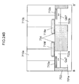
- FIGS. 24A , B, C and D show the cross-sectional structure taken along cut lines A-A', B-B', C-C' and D-D', respectively, in the layout diagram of FIG. 23 .
- the layout of the SRAM according to this embodiment will be described with reference to FIGS. 23 and 24A through 24D .
- This embodiment differs from the other embodiments in that the layout of the lower diffusion layers on the substrate that are the memory nodes is L-shaped.
- the diffusion layers are a rectangular shape as in the other embodiments.
- there is only one boundary line between the N+ doping regions 724a, 724b and the P+ doping region 725 that traverse the memory node the same as in Embodiment 5 and Embodiment 6, and moreover the pattern that forms the N+ doping regions 724a, 724b and the P+ doping region 725 is formed of simple line and space.
- the word line WL8 is wired in the horizontal direction and the bit lines BL8, BLB8 are wired in the vertical direction.
- Contacts 707a, 707b to the gates of the access transistors connected from the bit lines BL8, BLB8 can be shared with memory cells, which are not represented in the drawings, adjacent to the unit cell UC shown in FIG. 23 in the horizontal direction.
- the gate wiring extending from the gate electrodes of the driver transistor Qn48 and the load transistor Qp28 and the lower diffusion layers of the memory node Qa8 on the substrate are connected via a common contact 710a formed over both the gate wiring and the diffusion layers. Furthermore, the gate wiring extending from the gate electrodes of the driver transistor Qn38 and the load transistor Qp18 and the diffusion layers of the memory node Qb8 on the substrate are connected via a common contact 710b formed over both the gate wiring and the diffusion layers.
- the word line wiring, the bit line wiring, the power source potential wiring and the ground potential wiring are positioned in layers above the node connection wiring, which is the wiring within each memory cell, that is to say in layers above the contact 707a and the contact 707b, so as to be shared with the wiring of other memory cells.
- the node connection wiring is wired in the lower layer
- the word line WL8 and the ground potential wiring Vss8a, Vss8b are wired in the middle layer
- the bit line wiring BL8, BLB8 and the power source potential wiring Vcc8 are wired in the upper layer.
- a P-well which is a first well 701 a, is formed in the surface region of the substrate and the lower diffusion layers on the substrate are separated by an isolation layer 702.
- An N+ drain diffusion layer 703a is formed through conventional doping methods or the like in a first memory node Qa7 comprising the lower diffusion layers on the substrate, and an N+ drain diffusion layer 703b and a P+ drain diffusion layer 704b are respectively formed through conventional doping methods or the like in a second memory node Qb7 comprising the lower diffusion layers on the substrate.
- the P+ lower diffusion layer 704b which has the same conductive type as the first well 701a , is surrounded by an N-well that is a second anti-leak diffusion layer 701c having a conductive type differing from the first well 701a in order to control leakage to the substrate.
- Silicide layers 713a , 713b are formed in the surface region of the drain diffusion layers 703a , 703b, 704b, and the N+ lower diffusion layer 703b and the P+ lower diffusion layer 704b are connected through the silicide layer 713b which is not shown in the drawings.
- a columnar silicon layer 721a constructing an access transistor Qn18 is formed on the N+ drain diffusion layer 703a.
- a columnar silicon layer 723b constructing a load transistor Qp28 is formed on the P+ drain diffusion layer 704b, And, a columnar silicon layer 722b constructing a driver transistor Qn48 is formed on the N+ drain diffusion layer 703b.
- Gate insulating film 717 and gate electrode 718 are formed surrounding each of these columnar silicon layers.
- Source diffusion layers 714, 716 are formed through conventional doping methods or the like on the surface of the columnar silicon layers, and a silicide layer 715 is formed on the surface of the source diffusion layer.
- a contact 706a formed on the access transistor Qn18 is connected to the bit line BL8, a contact 707a formed on the gate wiring 718a extending from the gate electrode of the access transistor Qn18 is connected to the word line WL8, a contact 708b formed on the load transistor Qp28 is connected to the power source potential wiring Vcc8, a contact 709b formed on the driver transistor Qn48 is connected to the ground potential wiring Vss8, and the gate electrodes of the load transistor Qp28 and the driver transistor Qn48 are connected to each other via the gate wiring 718 extending from each of the gate electrodes.
- the P-well which is the first well 701a
- the P-well is formed in the surface region of the substrate and the lower diffusion layers on the substrate are separated by the isolation layer 702.
- the N+ drain diffusion layer 703a is formed through conventional doping methods or the like in the first memory node Qa7 comprising the lower diffusion layers on the substrate
- the N+ drain diffusion layer 703b is formed through conventional doping methods or the like in the second memory node Qb7 comprising the lower diffusion layers on the substrate
- the silicide layers 713a , 713b are formed in the surface region of the N+ drain diffusion layers.
- the drain diffusion layer 703a and the gate wiring 718f are connected through a common contact 710a formed over both the drain diffusion layer 703a and the gate wiring 718f .
- the drain diffusion layer 703b and the gate wiring 718e are connected through a common contact 710b formed over both the drain diffusion layer 703b and the gate wiring 718e .
- the P-well which is the first well 701a
- the N+ drain diffusion layer 703a is formed through conventional doping methods or the like on the first memory node Qa7 comprising the lower diffusion layers on t the substrate, and a silicide layer 713a is formed on the surface of the N+ drain diffusion layer 703a.
- the columnar silicon layer 721a constructing the access transistor Qn18 and the columnar silicon layer 722a constructing the driver transistor Qn38 are formed on the N+ drain diffusion layer 703a.
- Gate insulating film 717 and gate electrodes 718 are formed surrounding each of these columnar silicon layers.
- the source diffusion layer 714 is formed through conventional doping methods or the like on top of the columnar silicon layer, and a silicide layer 715 is formed on the surface of the source diffusion layer.
- a contact 706a formed on the access transistor Qn18 is connected to the bit line BL8 and a contact 709a formed on the driver transistor Qn38 is connected to the ground potential wiring Vss8 .
- the P-well which is a first well 701a
- the P+ drain diffusion layer 704a is formed through conventional doping methods or the like in the first memory node Qa7 comprising the lower diffusion layers on the substrate
- the P+ drain diffusion layer 704b is formed through conventional doping methods or the like in the second memory node Qb7 comprising the diffusion layers on the substrate.
- a first anti-leak N+ diffusion layer 701b having a conductive type differing from the first well 701a is formed at the bottom of the P+ drain diffusion layer 704a, which has the same conductive type as the first well 701a , in order to control leakage to the substrate
- a first anti-leak N+ diffusion layer 701c having a conductive type differing from the first well 701a is formed at the bottom of the P+ drain diffusion layer 704b, which has the same conductive type as the first well 701a , in order to control leakage to the substrate.
- the columnar silicon layer 723b constructing the load transistor Qp28 is formed on the drain diffusion layer 704b, and the columnar silicon layer 723a constructing the load transistor Qp18 is formed on the drain diffusion layer 704a .
- Gate insulating film 717 and gate electrodes 718 are formed surrounding each of these columnar silicon layers, the P+ source diffusion layer 716 is formed through conventional doping methods or the like on the surface of these columnar silicon layers, and a silicide layer 715 is formed on the surface of the source diffusion layer.
- the contacts 708b, 708a formed on the load transistor Qp28 and the load transistor Qp18 are connected to the power source potential wiring Vcc8 .
- the N+ drain diffusion layer and the P+ drain diffusion layer formed in the memory nodes on the substrate are directly connected through the silicide layer formed on the surface of the respective diffusion layer, which is similar to the embodiments described above.
- This allows the drain diffusion layers that are common among the access transistor, the driver transistor, and the load transistor to serve as SRAM memory nodes. Consequently, an isolation layer for separating the N+ source drain diffusion layer and the P+ source drain diffusion layer, which is necessary in conventional planar transistors, is not needed. Because it is sufficient only to separate the two memory nodes of the SRAM with the isolation layer, it is possible to attain an extremely small SRAM cell surface area.
- the static memory cells comprising six MOS transistors serve as SRAM memory nodes by the MOS transistors being formed of SGTs in which the drain, the gate and the source are positioned in the vertical direction.
- the first well is formed in the surface region of the substrate.
- the N+ source diffusion layer and the P+ source diffusion layer formed on the substrate are directly connected by a silicide layer formed on their surface, and the various drain diffusion layers of the same conductive type as the first well are surrounded by the first and second anti-leak diffusion layers shallower than the first well and having a conductive type opposite the first well.
- CMOS-type 6T-SRAM having an extremely small memory cell surface area because the isolation layer for separating the N+ source drain diffusion layer and the P+ source drain diffusion layer that are necessary in a conventional planer transistor is not needed.
- An isolation layer for separating the two memory nodes of the SRAM is sufficient.
Landscapes
- Semiconductor Memories (AREA)
Applications Claiming Priority (1)
| Application Number | Priority Date | Filing Date | Title |
|---|---|---|---|
| JP2009123882 | 2009-05-22 |
Publications (3)
| Publication Number | Publication Date |
|---|---|
| EP2254149A2 true EP2254149A2 (de) | 2010-11-24 |
| EP2254149A3 EP2254149A3 (de) | 2011-01-05 |
| EP2254149B1 EP2254149B1 (de) | 2014-08-06 |
Family
ID=42341366
Family Applications (1)
| Application Number | Title | Priority Date | Filing Date |
|---|---|---|---|
| EP10005356.0A Not-in-force EP2254149B1 (de) | 2009-05-22 | 2010-05-21 | SRAM mit vertikalen Transistoren mit einer Diffusionsschicht zur Verminderung von Leckströmen |
Country Status (6)
| Country | Link |
|---|---|
| US (1) | US8373235B2 (de) |
| EP (1) | EP2254149B1 (de) |
| KR (1) | KR101147582B1 (de) |
| CN (1) | CN101924108B (de) |
| SG (1) | SG166752A1 (de) |
| TW (1) | TWI402973B (de) |
Cited By (4)
| Publication number | Priority date | Publication date | Assignee | Title |
|---|---|---|---|---|
| EP3158577A4 (de) * | 2014-06-23 | 2018-07-11 | Synopsys, Inc. | Speicherzellen und logikzellen mit transistoren mit unterschiedlicher anzahl von nanodrähten oder 2d-materialstreifen |
| EP3435413A1 (de) * | 2017-07-28 | 2019-01-30 | IMEC vzw | Halbleiterbauelement und verfahren zur herstellung des halbleiterbauelements |
| US10256223B2 (en) | 2014-06-23 | 2019-04-09 | Synopsys, Inc. | Cells having transistors and interconnects including nanowires or 2D material strips |
| US10312229B2 (en) | 2016-10-28 | 2019-06-04 | Synopsys, Inc. | Memory cells including vertical nanowire transistors |
Families Citing this family (41)
| Publication number | Priority date | Publication date | Assignee | Title |
|---|---|---|---|---|
| GB2452732A (en) * | 2007-09-12 | 2009-03-18 | Seiko Epson Corp | Smart-card chip with organic conductive surface layer for detecting invasive attack |
| US9675443B2 (en) | 2009-09-10 | 2017-06-13 | Johnson & Johnson Vision Care, Inc. | Energized ophthalmic lens including stacked integrated components |
| US8950862B2 (en) * | 2011-02-28 | 2015-02-10 | Johnson & Johnson Vision Care, Inc. | Methods and apparatus for an ophthalmic lens with functional insert layers |
| US9233513B2 (en) | 2011-03-18 | 2016-01-12 | Johnson & Johnson Vision Care, Inc. | Apparatus for manufacturing stacked integrated component media inserts for ophthalmic devices |
| US10451897B2 (en) | 2011-03-18 | 2019-10-22 | Johnson & Johnson Vision Care, Inc. | Components with multiple energization elements for biomedical devices |
| US9698129B2 (en) | 2011-03-18 | 2017-07-04 | Johnson & Johnson Vision Care, Inc. | Stacked integrated component devices with energization |
| US9110310B2 (en) | 2011-03-18 | 2015-08-18 | Johnson & Johnson Vision Care, Inc. | Multiple energization elements in stacked integrated component devices |
| US9804418B2 (en) | 2011-03-21 | 2017-10-31 | Johnson & Johnson Vision Care, Inc. | Methods and apparatus for functional insert with power layer |
| US8857983B2 (en) | 2012-01-26 | 2014-10-14 | Johnson & Johnson Vision Care, Inc. | Ophthalmic lens assembly having an integrated antenna structure |
| CN103247628B (zh) * | 2012-02-06 | 2016-06-15 | 无锡华润上华半导体有限公司 | Sram器件及其制造方法 |
| JP5872054B2 (ja) * | 2013-06-17 | 2016-03-01 | ユニサンティス エレクトロニクス シンガポール プライベート リミテッドUnisantis Electronics Singapore Pte Ltd. | 半導体装置の製造方法、及び、半導体装置 |
| JP6121837B2 (ja) * | 2013-08-02 | 2017-04-26 | ソニーセミコンダクタソリューションズ株式会社 | 撮像素子 |
| US9356020B2 (en) * | 2013-09-12 | 2016-05-31 | Taiwan Semiconductor Manufacturing Company Limited | Semiconductor arrangement |
| WO2015059789A1 (ja) * | 2013-10-23 | 2015-04-30 | ユニサンティス エレクトロニクス シンガポール プライベート リミテッド | 半導体装置 |
| KR102178732B1 (ko) * | 2013-12-20 | 2020-11-13 | 삼성전자주식회사 | 반도체 소자 |
| JP6667215B2 (ja) * | 2014-07-24 | 2020-03-18 | キヤノン株式会社 | X線遮蔽格子、構造体、トールボット干渉計、x線遮蔽格子の製造方法 |
| US10627651B2 (en) | 2014-08-21 | 2020-04-21 | Johnson & Johnson Vision Care, Inc. | Methods and apparatus to form biocompatible energization primary elements for biomedical devices with electroless sealing layers |
| US10381687B2 (en) | 2014-08-21 | 2019-08-13 | Johnson & Johnson Vision Care, Inc. | Methods of forming biocompatible rechargable energization elements for biomedical devices |
| US9599842B2 (en) | 2014-08-21 | 2017-03-21 | Johnson & Johnson Vision Care, Inc. | Device and methods for sealing and encapsulation for biocompatible energization elements |
| US9793536B2 (en) | 2014-08-21 | 2017-10-17 | Johnson & Johnson Vision Care, Inc. | Pellet form cathode for use in a biocompatible battery |
| US10361404B2 (en) | 2014-08-21 | 2019-07-23 | Johnson & Johnson Vision Care, Inc. | Anodes for use in biocompatible energization elements |
| US9383593B2 (en) | 2014-08-21 | 2016-07-05 | Johnson & Johnson Vision Care, Inc. | Methods to form biocompatible energization elements for biomedical devices comprising laminates and placed separators |
| US9715130B2 (en) | 2014-08-21 | 2017-07-25 | Johnson & Johnson Vision Care, Inc. | Methods and apparatus to form separators for biocompatible energization elements for biomedical devices |
| US9941547B2 (en) | 2014-08-21 | 2018-04-10 | Johnson & Johnson Vision Care, Inc. | Biomedical energization elements with polymer electrolytes and cavity structures |
| US10361405B2 (en) | 2014-08-21 | 2019-07-23 | Johnson & Johnson Vision Care, Inc. | Biomedical energization elements with polymer electrolytes |
| US9659941B2 (en) | 2015-06-30 | 2017-05-23 | Globalfoundries Inc. | Integrated circuit structure with methods of electrically connecting same |
| US10345620B2 (en) | 2016-02-18 | 2019-07-09 | Johnson & Johnson Vision Care, Inc. | Methods and apparatus to form biocompatible energization elements incorporating fuel cells for biomedical devices |
| US10229917B2 (en) * | 2016-07-29 | 2019-03-12 | International Business Machines Corporation | Thin SRAM cell having vertical transistors |
| KR102741402B1 (ko) * | 2017-02-27 | 2024-12-11 | 삼성전자주식회사 | 수직형 반도체 소자 |
| US10490558B2 (en) * | 2017-05-31 | 2019-11-26 | Qualcomm Incorporated | Reducing or avoiding mechanical stress in static random access memory (SRAM) strap cells |
| US10804148B2 (en) | 2017-08-25 | 2020-10-13 | International Business Machines Corporation | Buried contact to provide reduced VFET feature-to-feature tolerance requirements |
| CN111344841B (zh) * | 2017-11-01 | 2023-07-04 | 新加坡优尼山帝斯电子私人有限公司 | 柱状半导体装置、及其制造方法 |
| US10381355B2 (en) * | 2018-01-11 | 2019-08-13 | International Business Machines Corporation | Dense vertical field effect transistor structure |
| KR102529229B1 (ko) | 2018-06-07 | 2023-05-04 | 삼성전자주식회사 | 반도체 소자 |
| US10566453B2 (en) * | 2018-06-29 | 2020-02-18 | International Business Machines Corporation | Vertical transistor contact for cross-coupling in a memory cell |
| US20210242025A1 (en) * | 2020-02-05 | 2021-08-05 | Samsung Electronics Co., Ltd. | Silicidation of source/drain region of vertical field effect transistor (vfet) structure |
| WO2022097251A1 (ja) * | 2020-11-06 | 2022-05-12 | ユニサンティス エレクトロニクス シンガポール プライベート リミテッド | 柱状半導体素子を用いたメモリ装置と、その製造方法 |
| WO2022157954A1 (ja) * | 2021-01-25 | 2022-07-28 | ユニサンティス エレクトロニクス シンガポール プライベート リミテッド | 半導体素子メモリ装置 |
| WO2022176181A1 (ja) * | 2021-02-22 | 2022-08-25 | ユニサンティス エレクトロニクス シンガポール プライベート リミテッド | 半導体素子を用いたメモリ装置 |
| CN116648061B (zh) * | 2023-06-09 | 2024-12-06 | 长鑫存储技术有限公司 | 存储单元、存储阵列及存储阵列的形成方法 |
| CN119997554B (zh) * | 2023-11-09 | 2026-03-31 | 北京超弦存储器研究院 | 半导体结构、存储器及其制造方法、电子设备 |
Citations (2)
| Publication number | Priority date | Publication date | Assignee | Title |
|---|---|---|---|---|
| JPH02188966A (ja) | 1989-01-17 | 1990-07-25 | Toshiba Corp | Mos型半導体装置 |
| JPH0799311A (ja) | 1993-05-12 | 1995-04-11 | Mitsubishi Electric Corp | 半導体装置およびその製造方法 |
Family Cites Families (19)
| Publication number | Priority date | Publication date | Assignee | Title |
|---|---|---|---|---|
| JPS60128654A (ja) | 1983-12-16 | 1985-07-09 | Hitachi Ltd | 半導体集積回路 |
| JPS63239973A (ja) | 1986-10-08 | 1988-10-05 | テキサス インスツルメンツ インコーポレイテツド | 集積回路およびその製造方法 |
| JPH03225873A (ja) | 1990-01-30 | 1991-10-04 | Mitsubishi Electric Corp | 半導体装置 |
| JP2748072B2 (ja) | 1992-07-03 | 1998-05-06 | 三菱電機株式会社 | 半導体装置およびその製造方法 |
| JP3428240B2 (ja) * | 1995-07-31 | 2003-07-22 | 三菱電機株式会社 | 半導体記憶装置 |
| JPH1079482A (ja) | 1996-08-09 | 1998-03-24 | Rai Hai | 超高密度集積回路 |
| US6304483B1 (en) | 1998-02-24 | 2001-10-16 | Micron Technology, Inc. | Circuits and methods for a static random access memory using vertical transistors |
| JP4674386B2 (ja) | 1999-02-17 | 2011-04-20 | ソニー株式会社 | 半導体記憶装置 |
| US6903411B1 (en) | 2000-08-25 | 2005-06-07 | Agere Systems Inc. | Architecture for circuit connection of a vertical transistor |
| US7138685B2 (en) * | 2002-12-11 | 2006-11-21 | International Business Machines Corporation | Vertical MOSFET SRAM cell |
| KR100467027B1 (ko) | 2003-01-07 | 2005-01-24 | 삼성전자주식회사 | 수직 트랜지스터로 구성된 에스램 소자 및 그 제조방법 |
| US6992916B2 (en) * | 2003-06-13 | 2006-01-31 | Taiwan Semiconductor Manufacturing Co., Ltd. | SRAM cell design with high resistor CMOS gate structure for soft error rate improvement |
| JP2005078741A (ja) | 2003-09-02 | 2005-03-24 | Renesas Technology Corp | 半導体記憶装置 |
| US6934182B2 (en) * | 2003-10-03 | 2005-08-23 | International Business Machines Corporation | Method to improve cache capacity of SOI and bulk |
| KR100537103B1 (ko) | 2003-12-27 | 2005-12-16 | 동부아남반도체 주식회사 | 수직형 트랜지스터의 제조방법 |
| US7420854B2 (en) * | 2006-07-26 | 2008-09-02 | Taiwan Semiconductor Manufacturing Co., Ltd. | SRAM device and operating method |
| JP5114968B2 (ja) | 2007-02-20 | 2013-01-09 | 富士通セミコンダクター株式会社 | 半導体装置及びその製造方法 |
| US7671422B2 (en) * | 2007-05-04 | 2010-03-02 | Taiwan Semiconductor Manufacturing Company, Ltd. | Pseudo 6T SRAM cell |
| WO2009060934A1 (ja) | 2007-11-07 | 2009-05-14 | Nec Corporation | 半導体装置及びその製造方法 |
-
2010
- 2010-05-21 SG SG201003556-6A patent/SG166752A1/en unknown
- 2010-05-21 US US12/784,826 patent/US8373235B2/en active Active
- 2010-05-21 EP EP10005356.0A patent/EP2254149B1/de not_active Not-in-force
- 2010-05-24 TW TW099116467A patent/TWI402973B/zh active
- 2010-05-24 KR KR1020100047888A patent/KR101147582B1/ko not_active Expired - Fee Related
- 2010-05-24 CN CN2010101891039A patent/CN101924108B/zh active Active
Patent Citations (2)
| Publication number | Priority date | Publication date | Assignee | Title |
|---|---|---|---|---|
| JPH02188966A (ja) | 1989-01-17 | 1990-07-25 | Toshiba Corp | Mos型半導体装置 |
| JPH0799311A (ja) | 1993-05-12 | 1995-04-11 | Mitsubishi Electric Corp | 半導体装置およびその製造方法 |
Cited By (5)
| Publication number | Priority date | Publication date | Assignee | Title |
|---|---|---|---|---|
| EP3158577A4 (de) * | 2014-06-23 | 2018-07-11 | Synopsys, Inc. | Speicherzellen und logikzellen mit transistoren mit unterschiedlicher anzahl von nanodrähten oder 2d-materialstreifen |
| US10256223B2 (en) | 2014-06-23 | 2019-04-09 | Synopsys, Inc. | Cells having transistors and interconnects including nanowires or 2D material strips |
| US10312229B2 (en) | 2016-10-28 | 2019-06-04 | Synopsys, Inc. | Memory cells including vertical nanowire transistors |
| EP3435413A1 (de) * | 2017-07-28 | 2019-01-30 | IMEC vzw | Halbleiterbauelement und verfahren zur herstellung des halbleiterbauelements |
| US11257823B2 (en) | 2017-07-28 | 2022-02-22 | Imec Vzw | Semiconductor device having vertical transistors and method of forming same |
Also Published As
| Publication number | Publication date |
|---|---|
| CN101924108B (zh) | 2012-03-28 |
| KR101147582B1 (ko) | 2012-05-21 |
| CN101924108A (zh) | 2010-12-22 |
| TWI402973B (zh) | 2013-07-21 |
| SG166752A1 (en) | 2010-12-29 |
| EP2254149B1 (de) | 2014-08-06 |
| KR20100126225A (ko) | 2010-12-01 |
| TW201104841A (en) | 2011-02-01 |
| US20100295135A1 (en) | 2010-11-25 |
| US8373235B2 (en) | 2013-02-12 |
| EP2254149A3 (de) | 2011-01-05 |
Similar Documents
| Publication | Publication Date | Title |
|---|---|---|
| EP2254149B1 (de) | SRAM mit vertikalen Transistoren mit einer Diffusionsschicht zur Verminderung von Leckströmen | |
| JP4756221B2 (ja) | 半導体記憶装置 | |
| EP2296176B1 (de) | SRAM-Zelle mit vier SGTs und entsprechendes Herstellungsverfahren | |
| KR101146869B1 (ko) | 반도체 기억장치 | |
| KR101182025B1 (ko) | 반도체 기억장치 | |
| EP2299485A1 (de) | SRAM-Zelle mit vier NMOS-SGTs und zwei Lastwiderständen | |
| JP5715209B2 (ja) | 半導体記憶装置 | |
| KR20130116334A (ko) | 반도체 기억 장치 | |
| JP5382939B2 (ja) | 半導体記憶装置 | |
| JP5489272B2 (ja) | 半導体記憶装置 | |
| KR20130118949A (ko) | 반도체 기억 장치 | |
| JPWO2013121537A1 (ja) | 半導体記憶装置 | |
| JPWO2013121536A1 (ja) | 半導体記憶装置 |
Legal Events
| Date | Code | Title | Description |
|---|---|---|---|
| PUAI | Public reference made under article 153(3) epc to a published international application that has entered the european phase |
Free format text: ORIGINAL CODE: 0009012 |
|
| AK | Designated contracting states |
Kind code of ref document: A2 Designated state(s): AL AT BE BG CH CY CZ DE DK EE ES FI FR GB GR HR HU IE IS IT LI LT LU LV MC MK MT NL NO PL PT RO SE SI SK SM TR |
|
| AX | Request for extension of the european patent |
Extension state: BA ME RS |
|
| PUAL | Search report despatched |
Free format text: ORIGINAL CODE: 0009013 |
|
| AK | Designated contracting states |
Kind code of ref document: A3 Designated state(s): AL AT BE BG CH CY CZ DE DK EE ES FI FR GB GR HR HU IE IS IT LI LT LU LV MC MK MT NL NO PL PT RO SE SI SK SM TR |
|
| AX | Request for extension of the european patent |
Extension state: BA ME RS |
|
| RIC1 | Information provided on ipc code assigned before grant |
Ipc: H01L 21/336 20060101ALI20101126BHEP Ipc: H01L 29/10 20060101ALI20101126BHEP Ipc: H01L 29/423 20060101ALI20101126BHEP Ipc: H01L 29/78 20060101ALI20101126BHEP Ipc: H01L 21/768 20060101ALI20101126BHEP Ipc: H01L 21/8238 20060101ALI20101126BHEP Ipc: H01L 21/8244 20060101AFI20100727BHEP Ipc: H01L 27/11 20060101ALI20101126BHEP |
|
| 17P | Request for examination filed |
Effective date: 20110531 |
|
| 17Q | First examination report despatched |
Effective date: 20110727 |
|
| RAP1 | Party data changed (applicant data changed or rights of an application transferred) |
Owner name: UNISANTIS ELECTRONICS SINGAPORE PTE. LTD. |
|
| RAP1 | Party data changed (applicant data changed or rights of an application transferred) |
Owner name: UNISANTIS ELECTRONICS SINGAPORE PTE. LTD. |
|
| GRAP | Despatch of communication of intention to grant a patent |
Free format text: ORIGINAL CODE: EPIDOSNIGR1 |
|
| RIC1 | Information provided on ipc code assigned before grant |
Ipc: H01L 29/78 20060101ALI20140326BHEP Ipc: H01L 21/8244 20060101AFI20140326BHEP Ipc: H01L 29/10 20060101ALI20140326BHEP Ipc: H01L 21/336 20060101ALI20140326BHEP Ipc: H01L 27/11 20060101ALI20140326BHEP Ipc: H01L 27/088 20060101ALI20140326BHEP |
|
| INTG | Intention to grant announced |
Effective date: 20140423 |
|
| GRAS | Grant fee paid |
Free format text: ORIGINAL CODE: EPIDOSNIGR3 |
|
| GRAA | (expected) grant |
Free format text: ORIGINAL CODE: 0009210 |
|
| AK | Designated contracting states |
Kind code of ref document: B1 Designated state(s): AL AT BE BG CH CY CZ DE DK EE ES FI FR GB GR HR HU IE IS IT LI LT LU LV MC MK MT NL NO PL PT RO SE SI SK SM TR |
|
| REG | Reference to a national code |
Ref country code: GB Ref legal event code: FG4D |
|
| RIN1 | Information on inventor provided before grant (corrected) |
Inventor name: ARAI, SHINTARO Inventor name: MASUOKA, FUJIO |
|
| REG | Reference to a national code |
Ref country code: AT Ref legal event code: REF Ref document number: 681369 Country of ref document: AT Kind code of ref document: T Effective date: 20140815 Ref country code: CH Ref legal event code: EP |
|
| REG | Reference to a national code |
Ref country code: IE Ref legal event code: FG4D |
|
| REG | Reference to a national code |
Ref country code: DE Ref legal event code: R096 Ref document number: 602010017985 Country of ref document: DE Effective date: 20140918 |
|
| REG | Reference to a national code |
Ref country code: AT Ref legal event code: MK05 Ref document number: 681369 Country of ref document: AT Kind code of ref document: T Effective date: 20140806 |
|
| REG | Reference to a national code |
Ref country code: NL Ref legal event code: VDEP Effective date: 20140806 |
|
| REG | Reference to a national code |
Ref country code: LT Ref legal event code: MG4D |
|
| PG25 | Lapsed in a contracting state [announced via postgrant information from national office to epo] |
Ref country code: BG Free format text: LAPSE BECAUSE OF FAILURE TO SUBMIT A TRANSLATION OF THE DESCRIPTION OR TO PAY THE FEE WITHIN THE PRESCRIBED TIME-LIMIT Effective date: 20141106 Ref country code: LT Free format text: LAPSE BECAUSE OF FAILURE TO SUBMIT A TRANSLATION OF THE DESCRIPTION OR TO PAY THE FEE WITHIN THE PRESCRIBED TIME-LIMIT Effective date: 20140806 Ref country code: GR Free format text: LAPSE BECAUSE OF FAILURE TO SUBMIT A TRANSLATION OF THE DESCRIPTION OR TO PAY THE FEE WITHIN THE PRESCRIBED TIME-LIMIT Effective date: 20141107 Ref country code: NO Free format text: LAPSE BECAUSE OF FAILURE TO SUBMIT A TRANSLATION OF THE DESCRIPTION OR TO PAY THE FEE WITHIN THE PRESCRIBED TIME-LIMIT Effective date: 20141106 Ref country code: FI Free format text: LAPSE BECAUSE OF FAILURE TO SUBMIT A TRANSLATION OF THE DESCRIPTION OR TO PAY THE FEE WITHIN THE PRESCRIBED TIME-LIMIT Effective date: 20140806 Ref country code: SE Free format text: LAPSE BECAUSE OF FAILURE TO SUBMIT A TRANSLATION OF THE DESCRIPTION OR TO PAY THE FEE WITHIN THE PRESCRIBED TIME-LIMIT Effective date: 20140806 Ref country code: PT Free format text: LAPSE BECAUSE OF FAILURE TO SUBMIT A TRANSLATION OF THE DESCRIPTION OR TO PAY THE FEE WITHIN THE PRESCRIBED TIME-LIMIT Effective date: 20141209 Ref country code: ES Free format text: LAPSE BECAUSE OF FAILURE TO SUBMIT A TRANSLATION OF THE DESCRIPTION OR TO PAY THE FEE WITHIN THE PRESCRIBED TIME-LIMIT Effective date: 20140806 |
|
| PG25 | Lapsed in a contracting state [announced via postgrant information from national office to epo] |
Ref country code: AT Free format text: LAPSE BECAUSE OF FAILURE TO SUBMIT A TRANSLATION OF THE DESCRIPTION OR TO PAY THE FEE WITHIN THE PRESCRIBED TIME-LIMIT Effective date: 20140806 Ref country code: HR Free format text: LAPSE BECAUSE OF FAILURE TO SUBMIT A TRANSLATION OF THE DESCRIPTION OR TO PAY THE FEE WITHIN THE PRESCRIBED TIME-LIMIT Effective date: 20140806 Ref country code: IS Free format text: LAPSE BECAUSE OF FAILURE TO SUBMIT A TRANSLATION OF THE DESCRIPTION OR TO PAY THE FEE WITHIN THE PRESCRIBED TIME-LIMIT Effective date: 20141206 Ref country code: CY Free format text: LAPSE BECAUSE OF FAILURE TO SUBMIT A TRANSLATION OF THE DESCRIPTION OR TO PAY THE FEE WITHIN THE PRESCRIBED TIME-LIMIT Effective date: 20140806 Ref country code: NL Free format text: LAPSE BECAUSE OF FAILURE TO SUBMIT A TRANSLATION OF THE DESCRIPTION OR TO PAY THE FEE WITHIN THE PRESCRIBED TIME-LIMIT Effective date: 20140806 Ref country code: PL Free format text: LAPSE BECAUSE OF FAILURE TO SUBMIT A TRANSLATION OF THE DESCRIPTION OR TO PAY THE FEE WITHIN THE PRESCRIBED TIME-LIMIT Effective date: 20140806 Ref country code: LV Free format text: LAPSE BECAUSE OF FAILURE TO SUBMIT A TRANSLATION OF THE DESCRIPTION OR TO PAY THE FEE WITHIN THE PRESCRIBED TIME-LIMIT Effective date: 20140806 |
|
| PG25 | Lapsed in a contracting state [announced via postgrant information from national office to epo] |
Ref country code: DK Free format text: LAPSE BECAUSE OF FAILURE TO SUBMIT A TRANSLATION OF THE DESCRIPTION OR TO PAY THE FEE WITHIN THE PRESCRIBED TIME-LIMIT Effective date: 20140806 Ref country code: SK Free format text: LAPSE BECAUSE OF FAILURE TO SUBMIT A TRANSLATION OF THE DESCRIPTION OR TO PAY THE FEE WITHIN THE PRESCRIBED TIME-LIMIT Effective date: 20140806 Ref country code: CZ Free format text: LAPSE BECAUSE OF FAILURE TO SUBMIT A TRANSLATION OF THE DESCRIPTION OR TO PAY THE FEE WITHIN THE PRESCRIBED TIME-LIMIT Effective date: 20140806 Ref country code: RO Free format text: LAPSE BECAUSE OF FAILURE TO SUBMIT A TRANSLATION OF THE DESCRIPTION OR TO PAY THE FEE WITHIN THE PRESCRIBED TIME-LIMIT Effective date: 20140806 Ref country code: IT Free format text: LAPSE BECAUSE OF FAILURE TO SUBMIT A TRANSLATION OF THE DESCRIPTION OR TO PAY THE FEE WITHIN THE PRESCRIBED TIME-LIMIT Effective date: 20140806 Ref country code: EE Free format text: LAPSE BECAUSE OF FAILURE TO SUBMIT A TRANSLATION OF THE DESCRIPTION OR TO PAY THE FEE WITHIN THE PRESCRIBED TIME-LIMIT Effective date: 20140806 |
|
| REG | Reference to a national code |
Ref country code: DE Ref legal event code: R097 Ref document number: 602010017985 Country of ref document: DE |
|
| PLBE | No opposition filed within time limit |
Free format text: ORIGINAL CODE: 0009261 |
|
| STAA | Information on the status of an ep patent application or granted ep patent |
Free format text: STATUS: NO OPPOSITION FILED WITHIN TIME LIMIT |
|
| 26N | No opposition filed |
Effective date: 20150507 |
|
| PG25 | Lapsed in a contracting state [announced via postgrant information from national office to epo] |
Ref country code: SI Free format text: LAPSE BECAUSE OF FAILURE TO SUBMIT A TRANSLATION OF THE DESCRIPTION OR TO PAY THE FEE WITHIN THE PRESCRIBED TIME-LIMIT Effective date: 20140806 |
|
| REG | Reference to a national code |
Ref country code: CH Ref legal event code: PL |
|
| PG25 | Lapsed in a contracting state [announced via postgrant information from national office to epo] |
Ref country code: MC Free format text: LAPSE BECAUSE OF FAILURE TO SUBMIT A TRANSLATION OF THE DESCRIPTION OR TO PAY THE FEE WITHIN THE PRESCRIBED TIME-LIMIT Effective date: 20140806 Ref country code: LU Free format text: LAPSE BECAUSE OF FAILURE TO SUBMIT A TRANSLATION OF THE DESCRIPTION OR TO PAY THE FEE WITHIN THE PRESCRIBED TIME-LIMIT Effective date: 20150521 Ref country code: LI Free format text: LAPSE BECAUSE OF NON-PAYMENT OF DUE FEES Effective date: 20150531 Ref country code: CH Free format text: LAPSE BECAUSE OF NON-PAYMENT OF DUE FEES Effective date: 20150531 |
|
| REG | Reference to a national code |
Ref country code: IE Ref legal event code: MM4A |
|
| PG25 | Lapsed in a contracting state [announced via postgrant information from national office to epo] |
Ref country code: IE Free format text: LAPSE BECAUSE OF NON-PAYMENT OF DUE FEES Effective date: 20150521 |
|
| REG | Reference to a national code |
Ref country code: FR Ref legal event code: PLFP Year of fee payment: 7 |
|
| PG25 | Lapsed in a contracting state [announced via postgrant information from national office to epo] |
Ref country code: BE Free format text: LAPSE BECAUSE OF FAILURE TO SUBMIT A TRANSLATION OF THE DESCRIPTION OR TO PAY THE FEE WITHIN THE PRESCRIBED TIME-LIMIT Effective date: 20140806 |
|
| PG25 | Lapsed in a contracting state [announced via postgrant information from national office to epo] |
Ref country code: MT Free format text: LAPSE BECAUSE OF FAILURE TO SUBMIT A TRANSLATION OF THE DESCRIPTION OR TO PAY THE FEE WITHIN THE PRESCRIBED TIME-LIMIT Effective date: 20140806 |
|
| REG | Reference to a national code |
Ref country code: FR Ref legal event code: PLFP Year of fee payment: 8 |
|
| PG25 | Lapsed in a contracting state [announced via postgrant information from national office to epo] |
Ref country code: HU Free format text: LAPSE BECAUSE OF FAILURE TO SUBMIT A TRANSLATION OF THE DESCRIPTION OR TO PAY THE FEE WITHIN THE PRESCRIBED TIME-LIMIT; INVALID AB INITIO Effective date: 20100521 Ref country code: SM Free format text: LAPSE BECAUSE OF FAILURE TO SUBMIT A TRANSLATION OF THE DESCRIPTION OR TO PAY THE FEE WITHIN THE PRESCRIBED TIME-LIMIT Effective date: 20140806 |
|
| PG25 | Lapsed in a contracting state [announced via postgrant information from national office to epo] |
Ref country code: TR Free format text: LAPSE BECAUSE OF FAILURE TO SUBMIT A TRANSLATION OF THE DESCRIPTION OR TO PAY THE FEE WITHIN THE PRESCRIBED TIME-LIMIT Effective date: 20140806 |
|
| REG | Reference to a national code |
Ref country code: FR Ref legal event code: PLFP Year of fee payment: 9 |
|
| PG25 | Lapsed in a contracting state [announced via postgrant information from national office to epo] |
Ref country code: MK Free format text: LAPSE BECAUSE OF FAILURE TO SUBMIT A TRANSLATION OF THE DESCRIPTION OR TO PAY THE FEE WITHIN THE PRESCRIBED TIME-LIMIT Effective date: 20140806 |
|
| PG25 | Lapsed in a contracting state [announced via postgrant information from national office to epo] |
Ref country code: AL Free format text: LAPSE BECAUSE OF FAILURE TO SUBMIT A TRANSLATION OF THE DESCRIPTION OR TO PAY THE FEE WITHIN THE PRESCRIBED TIME-LIMIT Effective date: 20140806 |
|
| REG | Reference to a national code |
Ref country code: DE Ref legal event code: R079 Ref document number: 602010017985 Country of ref document: DE Free format text: PREVIOUS MAIN CLASS: H01L0021824400 Ipc: H10B0010000000 |
|
| PGFP | Annual fee paid to national office [announced via postgrant information from national office to epo] |
Ref country code: GB Payment date: 20240521 Year of fee payment: 15 |
|
| PGFP | Annual fee paid to national office [announced via postgrant information from national office to epo] |
Ref country code: DE Payment date: 20240521 Year of fee payment: 15 |
|
| PGFP | Annual fee paid to national office [announced via postgrant information from national office to epo] |
Ref country code: FR Payment date: 20240529 Year of fee payment: 15 |
|
| REG | Reference to a national code |
Ref country code: DE Ref legal event code: R119 Ref document number: 602010017985 Country of ref document: DE |
|
| GBPC | Gb: european patent ceased through non-payment of renewal fee |
Effective date: 20250521 |
|
| PG25 | Lapsed in a contracting state [announced via postgrant information from national office to epo] |
Ref country code: GB Free format text: LAPSE BECAUSE OF NON-PAYMENT OF DUE FEES Effective date: 20250521 |
|
| PG25 | Lapsed in a contracting state [announced via postgrant information from national office to epo] |
Ref country code: DE Free format text: LAPSE BECAUSE OF NON-PAYMENT OF DUE FEES Effective date: 20251202 |
|
| PG25 | Lapsed in a contracting state [announced via postgrant information from national office to epo] |
Ref country code: FR Free format text: LAPSE BECAUSE OF NON-PAYMENT OF DUE FEES Effective date: 20250531 |