EP2248922B1 - Feuille d'alliage en cuivre et son procédé de production - Google Patents
Feuille d'alliage en cuivre et son procédé de production Download PDFInfo
- Publication number
- EP2248922B1 EP2248922B1 EP10004288.6A EP10004288A EP2248922B1 EP 2248922 B1 EP2248922 B1 EP 2248922B1 EP 10004288 A EP10004288 A EP 10004288A EP 2248922 B1 EP2248922 B1 EP 2248922B1
- Authority
- EP
- European Patent Office
- Prior art keywords
- copper alloy
- alloy sheet
- crystal
- cold rolling
- mean
- Prior art date
- Legal status (The legal status is an assumption and is not a legal conclusion. Google has not performed a legal analysis and makes no representation as to the accuracy of the status listed.)
- Active
Links
- 229910000881 Cu alloy Inorganic materials 0.000 title claims description 248
- 238000004519 manufacturing process Methods 0.000 title claims description 20
- 239000013078 crystal Substances 0.000 claims description 324
- 238000000034 method Methods 0.000 claims description 108
- 238000005097 cold rolling Methods 0.000 claims description 101
- 238000011282 treatment Methods 0.000 claims description 93
- 238000005096 rolling process Methods 0.000 claims description 79
- 238000000137 annealing Methods 0.000 claims description 67
- PXHVJJICTQNCMI-UHFFFAOYSA-N Nickel Chemical compound [Ni] PXHVJJICTQNCMI-UHFFFAOYSA-N 0.000 claims description 65
- 230000009467 reduction Effects 0.000 claims description 58
- 230000008569 process Effects 0.000 claims description 46
- 239000010949 copper Substances 0.000 claims description 42
- 230000032683 aging Effects 0.000 claims description 40
- 238000002441 X-ray diffraction Methods 0.000 claims description 36
- 238000010438 heat treatment Methods 0.000 claims description 34
- 229910052710 silicon Inorganic materials 0.000 claims description 27
- 229910052759 nickel Inorganic materials 0.000 claims description 26
- 239000000463 material Substances 0.000 claims description 25
- 239000000203 mixture Substances 0.000 claims description 25
- 229910052802 copper Inorganic materials 0.000 claims description 22
- 239000011701 zinc Substances 0.000 claims description 22
- RYGMFSIKBFXOCR-UHFFFAOYSA-N Copper Chemical compound [Cu] RYGMFSIKBFXOCR-UHFFFAOYSA-N 0.000 claims description 21
- XEEYBQQBJWHFJM-UHFFFAOYSA-N Iron Chemical compound [Fe] XEEYBQQBJWHFJM-UHFFFAOYSA-N 0.000 claims description 19
- 239000000126 substance Substances 0.000 claims description 19
- 238000005098 hot rolling Methods 0.000 claims description 17
- 239000011777 magnesium Substances 0.000 claims description 16
- 239000011651 chromium Substances 0.000 claims description 14
- 239000010936 titanium Substances 0.000 claims description 14
- 238000002844 melting Methods 0.000 claims description 12
- 230000008018 melting Effects 0.000 claims description 12
- 238000005266 casting Methods 0.000 claims description 11
- 239000012535 impurity Substances 0.000 claims description 11
- 239000010703 silicon Substances 0.000 claims description 11
- 229910001122 Mischmetal Inorganic materials 0.000 claims description 10
- 229910052804 chromium Inorganic materials 0.000 claims description 10
- 229910052719 titanium Inorganic materials 0.000 claims description 10
- 229910052796 boron Inorganic materials 0.000 claims description 9
- 229910052698 phosphorus Inorganic materials 0.000 claims description 9
- 229910052790 beryllium Inorganic materials 0.000 claims description 8
- 229910052726 zirconium Inorganic materials 0.000 claims description 8
- FYYHWMGAXLPEAU-UHFFFAOYSA-N Magnesium Chemical compound [Mg] FYYHWMGAXLPEAU-UHFFFAOYSA-N 0.000 claims description 7
- 229910017052 cobalt Inorganic materials 0.000 claims description 7
- 239000010941 cobalt Substances 0.000 claims description 7
- GUTLYIVDDKVIGB-UHFFFAOYSA-N cobalt atom Chemical compound [Co] GUTLYIVDDKVIGB-UHFFFAOYSA-N 0.000 claims description 7
- 229910052749 magnesium Inorganic materials 0.000 claims description 7
- 229910052709 silver Inorganic materials 0.000 claims description 7
- 229910052718 tin Inorganic materials 0.000 claims description 7
- ZOXJGFHDIHLPTG-UHFFFAOYSA-N Boron Chemical compound [B] ZOXJGFHDIHLPTG-UHFFFAOYSA-N 0.000 claims description 6
- VYZAMTAEIAYCRO-UHFFFAOYSA-N Chromium Chemical compound [Cr] VYZAMTAEIAYCRO-UHFFFAOYSA-N 0.000 claims description 6
- OAICVXFJPJFONN-UHFFFAOYSA-N Phosphorus Chemical compound [P] OAICVXFJPJFONN-UHFFFAOYSA-N 0.000 claims description 6
- ATJFFYVFTNAWJD-UHFFFAOYSA-N Tin Chemical compound [Sn] ATJFFYVFTNAWJD-UHFFFAOYSA-N 0.000 claims description 6
- RTAQQCXQSZGOHL-UHFFFAOYSA-N Titanium Chemical compound [Ti] RTAQQCXQSZGOHL-UHFFFAOYSA-N 0.000 claims description 6
- ATBAMAFKBVZNFJ-UHFFFAOYSA-N beryllium atom Chemical compound [Be] ATBAMAFKBVZNFJ-UHFFFAOYSA-N 0.000 claims description 6
- 239000011574 phosphorus Substances 0.000 claims description 6
- 239000000843 powder Substances 0.000 claims description 6
- 239000004332 silver Substances 0.000 claims description 6
- 229910052725 zinc Inorganic materials 0.000 claims description 5
- HCHKCACWOHOZIP-UHFFFAOYSA-N Zinc Chemical compound [Zn] HCHKCACWOHOZIP-UHFFFAOYSA-N 0.000 claims description 4
- QCWXUUIWCKQGHC-UHFFFAOYSA-N Zirconium Chemical compound [Zr] QCWXUUIWCKQGHC-UHFFFAOYSA-N 0.000 claims description 4
- 229910052742 iron Inorganic materials 0.000 claims description 4
- WPBNNNQJVZRUHP-UHFFFAOYSA-L manganese(2+);methyl n-[[2-(methoxycarbonylcarbamothioylamino)phenyl]carbamothioyl]carbamate;n-[2-(sulfidocarbothioylamino)ethyl]carbamodithioate Chemical compound [Mn+2].[S-]C(=S)NCCNC([S-])=S.COC(=O)NC(=S)NC1=CC=CC=C1NC(=S)NC(=O)OC WPBNNNQJVZRUHP-UHFFFAOYSA-L 0.000 claims description 4
- 239000002994 raw material Substances 0.000 claims description 4
- 238000005452 bending Methods 0.000 description 137
- 230000035882 stress Effects 0.000 description 70
- 239000000243 solution Substances 0.000 description 52
- 238000003483 aging Methods 0.000 description 37
- 229910045601 alloy Inorganic materials 0.000 description 34
- 239000000956 alloy Substances 0.000 description 34
- 229910017876 Cu—Ni—Si Inorganic materials 0.000 description 28
- 238000012360 testing method Methods 0.000 description 28
- 235000019587 texture Nutrition 0.000 description 23
- 230000003247 decreasing effect Effects 0.000 description 18
- 230000001965 increasing effect Effects 0.000 description 17
- 230000000052 comparative effect Effects 0.000 description 15
- 235000019589 hardness Nutrition 0.000 description 14
- 239000006104 solid solution Substances 0.000 description 14
- XUIMIQQOPSSXEZ-UHFFFAOYSA-N Silicon Chemical compound [Si] XUIMIQQOPSSXEZ-UHFFFAOYSA-N 0.000 description 9
- 239000011572 manganese Substances 0.000 description 9
- 229910052751 metal Inorganic materials 0.000 description 9
- 239000002184 metal Substances 0.000 description 9
- 238000001953 recrystallisation Methods 0.000 description 8
- 238000000151 deposition Methods 0.000 description 7
- 238000009792 diffusion process Methods 0.000 description 6
- 229910001369 Brass Inorganic materials 0.000 description 5
- 229910018098 Ni-Si Inorganic materials 0.000 description 5
- 229910018529 Ni—Si Inorganic materials 0.000 description 5
- 239000010951 brass Substances 0.000 description 5
- 230000008021 deposition Effects 0.000 description 5
- 229910052748 manganese Inorganic materials 0.000 description 5
- BQCADISMDOOEFD-UHFFFAOYSA-N Silver Chemical compound [Ag] BQCADISMDOOEFD-UHFFFAOYSA-N 0.000 description 4
- 230000006866 deterioration Effects 0.000 description 4
- 230000002708 enhancing effect Effects 0.000 description 4
- 239000011159 matrix material Substances 0.000 description 4
- 238000001000 micrograph Methods 0.000 description 4
- 238000009749 continuous casting Methods 0.000 description 3
- 238000002474 experimental method Methods 0.000 description 3
- PWHULOQIROXLJO-UHFFFAOYSA-N Manganese Chemical compound [Mn] PWHULOQIROXLJO-UHFFFAOYSA-N 0.000 description 2
- 229910005487 Ni2Si Inorganic materials 0.000 description 2
- 238000013459 approach Methods 0.000 description 2
- 230000015572 biosynthetic process Effects 0.000 description 2
- 238000001816 cooling Methods 0.000 description 2
- 230000002542 deteriorative effect Effects 0.000 description 2
- 238000009826 distribution Methods 0.000 description 2
- 230000006872 improvement Effects 0.000 description 2
- 229910000765 intermetallic Inorganic materials 0.000 description 2
- 238000005259 measurement Methods 0.000 description 2
- 239000007769 metal material Substances 0.000 description 2
- 230000003287 optical effect Effects 0.000 description 2
- 238000005554 pickling Methods 0.000 description 2
- 238000005498 polishing Methods 0.000 description 2
- 230000001737 promoting effect Effects 0.000 description 2
- 238000007670 refining Methods 0.000 description 2
- VSZWPYCFIRKVQL-UHFFFAOYSA-N selanylidenegallium;selenium Chemical compound [Se].[Se]=[Ga].[Se]=[Ga] VSZWPYCFIRKVQL-UHFFFAOYSA-N 0.000 description 2
- 238000005482 strain hardening Methods 0.000 description 2
- 238000005728 strengthening Methods 0.000 description 2
- JBQYATWDVHIOAR-UHFFFAOYSA-N tellanylidenegermanium Chemical compound [Te]=[Ge] JBQYATWDVHIOAR-UHFFFAOYSA-N 0.000 description 2
- XLYOFNOQVPJJNP-UHFFFAOYSA-N water Substances O XLYOFNOQVPJJNP-UHFFFAOYSA-N 0.000 description 2
- 229910052684 Cerium Inorganic materials 0.000 description 1
- 229910052692 Dysprosium Inorganic materials 0.000 description 1
- 229910052779 Neodymium Inorganic materials 0.000 description 1
- 239000002253 acid Substances 0.000 description 1
- 229910052782 aluminium Inorganic materials 0.000 description 1
- XAGFODPZIPBFFR-UHFFFAOYSA-N aluminium Chemical compound [Al] XAGFODPZIPBFFR-UHFFFAOYSA-N 0.000 description 1
- 230000008901 benefit Effects 0.000 description 1
- 150000001875 compounds Chemical class 0.000 description 1
- 238000007796 conventional method Methods 0.000 description 1
- 230000007797 corrosion Effects 0.000 description 1
- 238000005260 corrosion Methods 0.000 description 1
- 238000005336 cracking Methods 0.000 description 1
- 238000005238 degreasing Methods 0.000 description 1
- 238000011161 development Methods 0.000 description 1
- 230000018109 developmental process Effects 0.000 description 1
- UREBDLICKHMUKA-CXSFZGCWSA-N dexamethasone Chemical compound C1CC2=CC(=O)C=C[C@]2(C)[C@]2(F)[C@@H]1[C@@H]1C[C@@H](C)[C@@](C(=O)CO)(O)[C@@]1(C)C[C@@H]2O UREBDLICKHMUKA-CXSFZGCWSA-N 0.000 description 1
- 229910052746 lanthanum Inorganic materials 0.000 description 1
- 229910052745 lead Inorganic materials 0.000 description 1
- 230000003647 oxidation Effects 0.000 description 1
- 238000007254 oxidation reaction Methods 0.000 description 1
- 239000002244 precipitate Substances 0.000 description 1
- 229910052761 rare earth metal Inorganic materials 0.000 description 1
- 238000011084 recovery Methods 0.000 description 1
- 238000005204 segregation Methods 0.000 description 1
- 238000010008 shearing Methods 0.000 description 1
- 239000010944 silver (metal) Substances 0.000 description 1
- 229910002058 ternary alloy Inorganic materials 0.000 description 1
- 230000037303 wrinkles Effects 0.000 description 1
- 229910052727 yttrium Inorganic materials 0.000 description 1
Images

Classifications
-
- C—CHEMISTRY; METALLURGY
- C22—METALLURGY; FERROUS OR NON-FERROUS ALLOYS; TREATMENT OF ALLOYS OR NON-FERROUS METALS
- C22C—ALLOYS
- C22C9/00—Alloys based on copper
- C22C9/06—Alloys based on copper with nickel or cobalt as the next major constituent
-
- C—CHEMISTRY; METALLURGY
- C22—METALLURGY; FERROUS OR NON-FERROUS ALLOYS; TREATMENT OF ALLOYS OR NON-FERROUS METALS
- C22C—ALLOYS
- C22C9/00—Alloys based on copper
-
- C—CHEMISTRY; METALLURGY
- C22—METALLURGY; FERROUS OR NON-FERROUS ALLOYS; TREATMENT OF ALLOYS OR NON-FERROUS METALS
- C22F—CHANGING THE PHYSICAL STRUCTURE OF NON-FERROUS METALS AND NON-FERROUS ALLOYS
- C22F1/00—Changing the physical structure of non-ferrous metals or alloys by heat treatment or by hot or cold working
- C22F1/08—Changing the physical structure of non-ferrous metals or alloys by heat treatment or by hot or cold working of copper or alloys based thereon
-
- H—ELECTRICITY
- H01—ELECTRIC ELEMENTS
- H01R—ELECTRICALLY-CONDUCTIVE CONNECTIONS; STRUCTURAL ASSOCIATIONS OF A PLURALITY OF MUTUALLY-INSULATED ELECTRICAL CONNECTING ELEMENTS; COUPLING DEVICES; CURRENT COLLECTORS
- H01R13/00—Details of coupling devices of the kinds covered by groups H01R12/70 or H01R24/00 - H01R33/00
- H01R13/02—Contact members
- H01R13/03—Contact members characterised by the material, e.g. plating, or coating materials
Definitions
- the present invention generally relates to a copper alloy sheet and a method for producing the same. Morespecifically,theinvention relates to a sheet of a copper alloy containing nickel and silicon (a sheet of a Cu-Ni-Si alloy), which is used as the material of electric and electronic parts, such as connectors, lead frames, relays and switches, and a method for producing the same.
- the materials used for electric and electronic parts as the materials of current-carrying parts are required to have a good electric conductivity in order to suppress the generation of Joule heat due to the carrying of current, as well as such a high strength that the materials can withstand the stress applied thereto during the assembly and operation of electric and electronic apparatuses using the parts.
- the materials used for electric and electronic parts, such as connectors are also required to have an excellent bending workability since the parts are generally formed by bending after press blanking.
- the materials used for the parts are required to have an excellent stress relaxation resistance, i.e., a resistance to such a phenomenon (stress relaxation) that the contact pressure between the parts is deteriorated with age.
- the sheets of copper and copper alloys serving as the materials of the parts are required to be thinned, so that the required strength level of the materials is more severe.
- the tensile strength of the materials is desired to be the strength level of not less than 700 MPa, preferably not less than 750 MPa, and more preferably not less than 800 MPa.
- copper alloy sheets used as the materials of electric and electronic parts, such as connectors, which are small and have complicated shapes are often formed by both of the good way bending and bad way bending. Therefore, it is strongly desired that the strength level of a copper alloy sheet is not only enhanced, but the anisotropy of the bending workability of the copper alloy sheet is also improved.
- the stress relaxation resistance of electric and electronic parts, such as connectors is particularly important when the parts are used for automobiles in high-temperature environments.
- the stress relaxation resistance is such a kind of creep phenomenon that the contact pressure on a spring portion of a material forming electric and electronic parts, such as connectors, is deteriorated with age in a relatively high-temperature (e.g., 100 to 200 °C) environment even if it is maintained to be a constant contact pressure at ordinary temperature.
- the stress relaxation resistance is such a phenomenon that the stress applied to a metal material is relaxed by plastic deformation produced by the movement of dislocation, which is caused by the self-diffusion of atoms forming a matrix and the diffusion of the solid solution of atoms, in such a state that the stress is applied to the metal material.
- a copper alloy sheet having a good strength, bending workability or stress relaxation resistance is suitably chosen in accordance with the use thereof as a material used for a current-carrying part, such as a connector.
- the sheets of Cu-Ni-Si alloys are noted as materials having a relatively excellent characteristic balance between the strength and electric conductivity thereof.
- the sheets of Cu-Ni-Si alloys can have the strength of not less than 700 MPa while maintaining a relatively high electric conductivity (30 to 50 %IACS) by a process basically comprising a solution treatment, cold-rolling, ageing treatment, finish cold-rolling and low-temperature annealing.
- the bending workability of the sheets of Cu-Ni-Si alloys is not always good since they have a high strength.
- the extent of work hardening is enhanced to remarkably deteriorate the bad way bending workability, so that there are some cases where the sheets can not be worked as electric and electronic parts, such as connectors, even if the strength and electric conductivity thereof are high.
- the solution treatment for the sheets of Cu-Ni-Si alloys is often carried out in a relatively low temperature range so as to cause part of deposits (or crystallized substances) for pinning the growth of recrystallized grains to remain, not in a high temperature range in which all of the deposits (or crystallized substances) are caused to form the solid solution thereof.
- the strength level of the sheets after the ageing treatment is necessarily lowered since the amount of the solid solution of Ni and Si is decreased although the crystal grains can be fined.
- the area of grain boundaries existing per a unit volume is increased as the crystal grain size is decreased, the fining of the crystal grains causes to promote stress relaxation being a kind of creep phenomenon.
- the diffusion rate along the grain boundaries of atoms is far higher than that in the grains, so that the deterioration of the stress relaxation resistance of the sheets due to grain refining causes a serious problem.
- the pattern of X-ray diffraction from the surface (rolled surface) of the sheet of a Cu-Ni-Si alloy generally comprises the peaks of diffraction on five crystal planes of ⁇ 111 ⁇ , ⁇ 200 ⁇ , ⁇ 220 ⁇ , ⁇ 311 ⁇ and ⁇ 422 ⁇ .
- the intensities of X-ray diffraction from other crystal planes are far smaller than those from the five crystal planes.
- the intensities of X-ray diffraction on the ⁇ 200 ⁇ , ⁇ 311 ⁇ and ⁇ 422 ⁇ planes are usually increased after a solution treatment (recrystallization).
- the intensities of X-ray diffraction on these planes are decreased by the subsequent cold rolling operation, so that the intensity of X-ray diffraction on the ⁇ 220 ⁇ plane is relatively increased.
- the intensity of X-ray diffraction on the ⁇ 111 ⁇ plane is not so varied by the cold rolling operation. Therefore, in the above described Japanese Patent Laid-Open Nos. 2006-9108 , 2006-16629 , 2006-152392 , 2000-80428 and 2006-9137 , the crystal orientation (fixture) of Cu-Ni-Si alloys is controlled by the intensities of X-ray diffraction from these crystal planes.
- the stress relaxation resistance of the sheets is often deteriorated since it is required to fine the crystal grains of the sheets to cause the sheets to have a mean crystal grain size of 10 ⁇ m or less.
- EP 1 997 920 A2 discloses a copper alloy for electric and electronic equipments containing from 0.5 to 4.0 mass% of nickel, from 0.5 to 2.0 mass% of cobalt and from 0.3 to 1.5 mass% of silicon, with the balance being copper and inevitable impurities, which has a certain diffraction intensity from the (200) plane.
- EP 0 949 343 A1 relates to a copper alloy sheet adapted for use as electronic part, which comprises 0.4 to 2.5 wt.% of nickel, 0.05 to 0.6 wt.% of silicon, 0.001 to 0.05 wt.% of magnesium and the balance being copper and inevitable impurities, wherein the average grain size in the sheet is in the range between 3 to 20 ⁇ m and the size of the intermetallic compound precipitate of nickel and silicon is in the range of 0.3 ⁇ m or less.
- the inventors have diligently studied and found that it is possible to improve the bending workability of a copper alloy sheet, which has a chemical composition containing 0.7 to 4.0 wt% of nickel, 0.2 to 1.5 wt% of silicon and the balance being copper and unavoidable impurities, while remarkably improving the anisotropy thereof without deteriorating the stress relaxation resistance thereof, by increasing the percentage of crystal grains of the ⁇ 200 ⁇ crystal plane orientation (Cube orientation) having a small anisotropy while decreasing the percentage of crystal grains of ⁇ 422 ⁇ crystal plane orientation having a great anisotropy, and that it is possible to improving both of the stress relaxation resistance and bending workability of the copper alloy sheet by enhancing the mean twin crystal density in the crystal grains thereof.
- the inventors have made the present invention.
- a copper alloy sheet having having a thickness of 0.05 to 1.0 mm and a chemical composition consisting of
- a method for produing a copper alloy sheet comprising:
- the method for producing a copper alloy sheet preferably further comprises a finish cold rolling step of carrying out a cold rolling operation at a rolling reduction of not higher than 50%, after the ageing treatment step wherein the cold rolling operation at the finish cold rolling step is carried out so as to satisfy 10 ⁇ ⁇ 2 ⁇ ⁇ (50 - ⁇ 1) / (100 - ⁇ 1) ⁇ x 100, assuming that the rolling reduction (%) in the intermediate cold rolling is ⁇ 1 and the rolling reduction (%) in the finish cold rolling is ⁇ 2.
- the method for producing a copper alloy sheet preferably further comprises a low temperature annealing step for carrying out a heat treatment at a temperature of 150 to 550 °C, after the finish cold rolling step.
- an electric and electronic part wherein the above-described copper alloy sheet is used as the material thereof.
- This electric and electronic part is preferably any one of a connector, a lead frame, a relay and a switch.
- the "mean crystal grain size obtained without including twin crystal boundaries by the method of section based on JIS H0501" means a true mean crystal grain size obtained without including twin crystal boundaries (i.e., without counting the number of twin crystal boundaries) when the number of crystal grains completely cut by line segments having well known lengths on an image or photograph of a microscope is counted to obtain the mean crystal grain size from the mean value of the cut lengths in accordance with the method of section based on JIS H0501.
- the "mean crystal grain size obtained while including twin crystal boundaries by the method of section based on JIS H0501" means a mean crystal grain size obtained while including twin crystal boundaries (i.e., while counting the number of twin crystal boundaries) when the number of crystal grains completely cut by line segments having well known lengths on an image or photograph of a microscope is counted to obtain the mean crystal grain size from the mean value of the cut lengths in accordance with the method of section based on in JIS H0501.
- the present invention it is possible to produce a Cu-Ni-Si alloy sheet having an excellent bending workability and an excellent stress relaxation resistance while maintaining a high strength which is a tensile strength of not less than 700 MPa, and particularly, having such a small anisotropy that the bending workability of the sheet is excellent in both of the good way and bad way.
- the preferred embodiment of a copper alloy sheet according to the present invention has a chemical composition consisting of: 0.7 to 4.0 wt% of nickel (Ni); 0.2 to 1.5 wt% of silicon (Si); optionally one or more elements which are selected from the group consisting of 0.1 to 1.2 wt% of tin (Sn), 2.0 wt% or less of zinc (Zn), 1.0 wt% or less of magnesium (Mg), 2.0 wt% or less of cobalt (Co) and 1.0 wt% or less of iron (Fe); optionally one or more elements which are selected from the group consisting of chromium (Cr), boron (B), phosphorus (P), zirconium (Zr), titanium (Ti), manganese (Mn), silver (Ag), beryllium (Be) and misch metal, the total amount of these elements being 3 wt% or less; and the balance being copper and unavoidable impurities.
- Ni nickel
- Si silicon
- the copper alloy sheet has a crystal orientation which satisfies I ⁇ 200 ⁇ / Io ⁇ 200 ⁇ ⁇ 1.0, assuming that the intensity of X-ray diffraction on the ⁇ 200 ⁇ crystal plane on the surface of the copper alloy sheet is I ⁇ 200 ⁇ and that the intensity of X-ray diffraction on the ⁇ 200 ⁇ crystal plane of the standard powder of pure copper is I 0 ⁇ 200 ⁇ , and which satisfies I ⁇ 200 ⁇ /I ⁇ 422 ⁇ ⁇ 15, assuming that the intensity of X-ray diffraction on the ⁇ 422 ⁇ crystal plane on the surface of the copper alloy sheet is I ⁇ 422 ⁇ .
- the mean crystal grain size D of the copper alloy sheet is in the range of from 6 ⁇ m to 60 ⁇ m, the mean crystal grain size D being obtained without including twin crystal boundaries while distinguishing crystal grain boundaries from the twin crystal boundaries on the surface of the copper alloy sheet by the method of section based on JIS H0501.
- the tensile strength of the copper alloy sheet is preferably not less than 700 MPa.
- the copper alloy sheet preferably has a crystal orientation which satisfies I ⁇ 200 ⁇ /I ⁇ 422 ⁇ ⁇ 50.
- the preferred embodiment of a copper alloy sheet according to the present invention is a sheet of a Cu-Ni-Si alloy containing Cu, Ni and Si.
- the copper alloy sheet may optionally contain a small amount of Sn, Zn and other elements in addition to the three basic elements of the Cu-Ni-Si ternary alloy.
- Nickel (Ni) and silicon (Si) have the functions of generating Ni-Si deposits to improve the strength and electric conductivity of the copper alloy sheet. If the content of Ni is less than 0.7 wt% and/or if the content of Si is less than 0.2 wt%, it is difficult to sufficiently provide these functions. Therefore, the content of Ni is preferably not less than 0.7 wt%, more preferably not less than 1.2 wt%, and most preferably not less than 1.5 wt%.
- the content of Si is preferably not less than 0.2 wt%, more preferably not less than 0.3 wt%, and most preferably not less than 0.35 wt%.
- the content of Ni is preferably not higher than 4.0 wt%, more preferably not higher than 3.5 wt%, and most preferably not higher than 2.5 wt%.
- the content of Si is preferably not higher than 1.5 wt%, more preferably not higher than 1.0 wt%, and most preferably not higher than 0.8 wt%.
- Ni-Si deposits formed by Ni and Si are intermetallic compounds mainly containing Ni 2 Si.
- an aging treatment does not always cause all of Ni and Si in the alloy to be deposits, and Ni and Si in the alloy exist as a solid solution in a Cu matrix to some extent.
- the solid solution of Ni and Si slightly improves the strength of the copper alloy sheet, the function of improving the strength of the copper alloy sheet is smaller than that of the deposits, and it causes to deteriorate the electric conductivity thereof.
- the ratio of the content of Ni to the content of Si is preferably close to the composition ratio of deposits Ni 2 Si.
- the mass ratio of Ni/Si is preferably adjusted to be in the range of from 3.5 to 6.0, and more preferably in the range of from 3.5 to 5.0.
- the mass ratio of Ni/Si is preferably adjusted to be in the range of from 1.0 to 4.0.
- Tin (Sn) has the function of carrying out the solid-solution strengthening (or hardening) of the copper alloy.
- the content of Sn is preferably not less than 0.1 wt%, and more preferably not less than 0.2 wt%.
- the content of Sn is preferably not higher than 1.2 wt%, and more preferably not higher than 0.7 wt%.
- Zinc (Zn) has the function of improving the castability of the copper alloy, in addition to the function of improving the solderability and strength thereof. If the copper alloy contains Zn, inexpensive brass scraps may be used. In order to sufficiently provide these functions, the content of Zn is preferably not less than 0.1 wt%, and more preferably not less than 0.3 wt%. However, if the content of Zn exceeds 2.0 wt%, the electric conductivity and stress corrosion cracking resistance of the copper alloy sheet are easily deteriorated. Therefore, if the copper alloy contains Zn, the content of Zn is preferably not higher than 2.0 wt%, and more preferably not higher than 1.0 wt%.
- Magnesium (Mg) has the functions of preventing Ni-Si deposits from being coarsened and of improving the stress relaxation resistance of the copper alloy sheet.
- the content of Mg is preferably not less than 0.01 wt%. However, if the content exceeds 1.0 wt%, the castability and hot-workability of the copper alloy are easily deteriorated. Therefore, if the copper alloy sheet contains Mg, the content of Mg is preferably not higher than 1.0 wt%.
- Co has the function of improving the strength and electric conductivity of the copper alloy sheet. That is, Co is an element capable of generating deposits with Si and of depositing alone. If the copper alloy sheet contains Co, it reacts with the solid solution of Si in the Cu matrix to generate deposits, and excessive Co deposits alone, so that the strength and electric conductivity thereof are improved. In order to sufficiently provide these functions, the content of Co is preferably not less than 0.1 wt%. However, Co is an expensive element, so that the content of Co is preferably not higher than 2.0 wt% since the costs are increased if the copper alloy sheet contains excessive Co.
- the content of Co is preferably in the range of from 0.1 wt% to 2.0 wt%, and more preferably in the range of from 0.5 wt% to 1.5 wt%.
- the copper alloy sheet preferably contains such an excessive amount of Si that the mass ratio of Si/Co is in the range of from 0.15 to 0.3, since there is some possibility that the amount of Si capable of generating Ni-Si deposits is decreased if deposits of Co and Si are generated.
- Iron (Fe) has the function of improving the bending workability of the copper alloy sheet by promoting the generation of the ⁇ 200 ⁇ orientation of recrystallized grains after a solution treatment and by suppressing the generation of the ⁇ 220 ⁇ orientation thereof. That is, if the copper alloy sheet contains Fe, the bending workability thereof is improved by the decrease of the ⁇ 220 ⁇ orientation density and the increase of the ⁇ 200 ⁇ orientation density.
- the content of Fe is preferably not less than 0.05wt%. However, if the content of Fe is excessive, the electric conductivity of the copper alloy sheet is remarkably lowered, so that the content of Fe is preferably not higher than 1.0 wt%. Therefore, if the copper alloy sheet contains Fe, the content of Fe is preferably in the range of from 0.05 wt% to 1.0 wt%, and more preferably in the range of from 0.1 wt% to 0.5 wt%.
- Cr chromium
- B boron
- P phosphorus
- Zr zirconium
- Ti titanium
- Mn manganese
- Ag silver
- Be beryllium
- Cr, B, P, Zr, Ti, Mn and Be have the functions of further enhancing the strength of the copper alloy sheet and of decreasing the stress relaxation thereof.
- the misch metal is a mixture of rare earth elements containing Ce, La, Dy, Nd, Y and so forth, and has the functions of refining crystal grains and of dispersing deposits.
- the total amount of these elements is preferably not less than 0.01 wt% in order to sufficiently provide the function of each element. However, if the total amount of these elements exceeds 3 wt%, the elements have a bad influence on the hot workability or cold workability thereof, and it is unfavorable with respect to costs. Therefore, the total amount of these elements is preferably not higher than 3 wt%, and more preferably not higher than 2 wt%.
- the texture of Cu-Ni-Si copper alloys generally comprises ⁇ 100 ⁇ 001>, ⁇ 110 ⁇ 112>, ⁇ 113 ⁇ 112>, ⁇ 112 ⁇ 111> and intermediate orientations thereof.
- the pattern of X-ray diffraction from a direction (ND) perpendicular to the surface (rolled surface) of the copper alloy sheets generally comprises the peaks of diffraction on four crystal planes of ⁇ 200 ⁇ , ⁇ 220 ⁇ , ⁇ 311 ⁇ and ⁇ 422 ⁇ .
- Schmid factors as indexes which indicate the probability of generating plastic deformation (slip) when an external force is applied to a crystal in a certain direction. Assuming that the angle between the direction of the external force applied to the crystal and the normal line to the slip plane is ⁇ and that the angle between the direction of the external force applied to the crystal and the slip direction is ⁇ , the Schmid factors are expressed by cos ⁇ ⁇ cos ⁇ , and the values thereof are not greater than 0.5. If the Schmid factor is greater (i.e., if the Schmid factor approaches 0.5), it means that shearing stress in slip directions is greater.
- the Schmid factor is greater (i.e., if the Schmid factor approaches 0.5) when an external force is applied to a crystal in a certain direction, the crystal is easily deformed.
- the crystal structure of Cu-Ni-Si alloys is the face centered cubic (fcc).
- the slip system of a face-centered cubic crystal has a slip plane of ⁇ 111 ⁇ and a slip direction of ⁇ 110>. The actual crystal is easily deformed to decrease the extent of work hardening as the Schmid factor is greater.
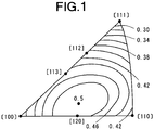
- FIG. 1 is a standard reversedpole figure which shows the Schmid factor distribution of a face-centered cubic crystal.
- the Schmid factor in the ⁇ 120> direction is 0.490 which is close to 0.5. That is, a face-centered cubic crystal is very easy to be deformed if an external force is applied to the crystal in the ⁇ 120> direction.
- the Schmid factors in other directions are 0.408 in the ⁇ 100> direction, 0.445 in the ⁇ 113> direction, 0.408 in the ⁇ 110> direction, 0.408 in the ⁇ 112> direction, and 0.272 in the ⁇ 111> direction.
- the ⁇ 200 ⁇ crystal plane ( ⁇ 100 ⁇ 001> orientation) has similar characteristics in the three directions of ND, LD and TD, and is generally called Cube orientation.
- the number of combinations of slip planes with slip directions, in which both of LD: ⁇ 001> and TD: ⁇ 010> can contribute to slip, is eight among twelve combinations, and all of the Schmid factors thereof are 0.41.
- the slip line on the ⁇ 200 ⁇ crystal plane allows the bending deformation of the copper alloy sheet without forming shear zones since it is possible to improve the symmetric properties of 45° and 135° with respect to the bending axis. That is, it was found that the Cube orientation causes the bending workability of the copper alloy sheet in both of the good way and bad way to be good, and does not cause any anisotropy.
- the Cube orientation is the principal orientation of a pure copper type recrystallized texture, it is difficult to develop the Cube orientation by a typical method for producing a copper alloy sheet.
- a copper alloy sheet having a crystal orientation, in which the Cube orientation is developed can be obtained by appropriately controlling the conditions in the process annealing and solution treatment.
- the ⁇ 220 ⁇ crystal plane ( ⁇ 110 ⁇ 112> orientation) is the principal orientation of a brass (alloy) type rolling texture, and is generally called Brass orientation (or B orientation).
- the LD of the B orientation is the ⁇ 112> direction, and the TD thereof is the ⁇ 111> direction.
- the Schmid factors in LD and Td are 0.408 and 0.272, respectively. That is, the bending workability in the bad way is generally deteriorated by the development of the B orientation with the increase of the finish rolling reduction. However, the finish rolling after the ageing treatment is effective in order to improve the strength of the copper alloy sheet.
- both of the strength of the copper alloy sheet and the bending workability in the bad way thereof can be improved by restricting the finish rolling reduction after the ageing treatment.
- the ⁇ 311 ⁇ crystal plane ( ⁇ 113 ⁇ 112> orientation) is the principal orientation of a brass (alloy) type rolling texture. If the ⁇ 113 ⁇ 112> orientation is developed, the bending workability of the copper alloy sheet in the bad way can be improved, but the bending workability thereof in the good way is deteriorated, so that the anisotropy in the bending workability is increased. As will be described later, in the preferred embodiment of a method for producing a copper alloy sheet according to the present invention, the Cube orientation after the solution treatment is developed to necessarily restrain the generation of the ⁇ 113 ⁇ 112> orientation, so that the anisotropy in the bending workability can be improved.
- I ⁇ 200 ⁇ / I ⁇ 422 ⁇ 9.
- I ⁇ 200 ⁇ / I ⁇ 422 ⁇ 2 to 5 which is low, so that it can be seen that the existing percentage of the ⁇ 422 ⁇ plane serving as the origin of cracks during bending is high.
- the ⁇ 422 ⁇ crystal plane ( ⁇ 112 ⁇ 111> orientation) is the principal orientation of a pure copper type rolling texture.
- the conditions in the process annealing and solution treatment are appropriately controlled, so that the percentage of the ⁇ 422 ⁇ crystal plane existing after the solution treatment can be decreased to obtain the crystal orientation satisfying I ⁇ 200 ⁇ / I ⁇ 422 ⁇ ⁇ 15.
- the percentage of the existing ⁇ 422 ⁇ crystal plane is further decreased to obtain the crystal orientation satisfying I ⁇ 200 ⁇ / I ⁇ 422 ⁇ ⁇ 50, the bending workability in both of the good way and bad way can be remarkably improved even if the copper alloy plate has a tensile strength of not less than 800 MPa.
- the bending workability of a Cu-Ni-Si copper alloy sheet in both of the good way and bad way can be improved so that the anisotropy in the bending workability can be improved, if the texture having the ⁇ 200 ⁇ crystal plane (Cube orientation) as a principal orientation component is stronger by the solution treatment.
- the copper alloy sheet has a crystal orientation which preferably satisfies I ⁇ 200 ⁇ / I 0 ⁇ 200 ⁇ ⁇ 1.0, more preferably satisfies I ⁇ 200 ⁇ / I 0 ⁇ 200 ⁇ ⁇ 1.5, and most preferably satisfies I ⁇ 200 ⁇ / I 0 ⁇ 200 ⁇ ⁇ 2.0, assuming that the intensity of X-ray diffraction on the ⁇ 200 ⁇ crystal plane on the surface of the copper alloy sheet is I ⁇ 200 ⁇ and that the intensity of X-ray diffraction on the ⁇ 200 ⁇ crystal plane of the standard powder of pure copper is I 0 ⁇ 200 ⁇ .
- the copper alloy sheet Since the ⁇ 422 ⁇ crystal plane causes the deterioration of the bending workability of the copper alloy sheet even if the amount thereof is small, it is required to maintain the high strength and excellent bending workability of the copper alloy sheet by maintaining the low volume percentage of the ⁇ 422 ⁇ crystal plane after the solution treatment. Therefore, the copper alloy sheet has a crystal orientation which satisfies I ⁇ 200 ⁇ / I ⁇ 422 ⁇ ⁇ 15, assuming that the intensity of X-ray diffraction on the ⁇ 422 ⁇ crystal plane on the surface of the copper alloy sheet is I ⁇ 422 ⁇ .
- the I ⁇ 200 ⁇ / I ⁇ 422 ⁇ is too small, the properties of the recrystallized texture having ⁇ 422 ⁇ crystal plane as a principal orientation are relatively dominant, so that the bending workability of the copper alloy sheet is remarkably deteriorated.
- the I ⁇ 200 ⁇ / I ⁇ 422 ⁇ is large, the bending workability of the copper alloy sheet in both of the LD and TD is remarkably improved.
- the strength of the copper alloy sheet is enhanced to be a tensile strength of not less than 800 MPa, it is required to further improve the bending workability, so that the crystal orientation preferably satisfies I ⁇ 200 ⁇ / I ⁇ 422 ⁇ ⁇ 50.
- crystal grains are not uniformly deformed since there are crystal grains, which are easy to be deformed during bending, and crystal grains, which are difficult to be deformed during bending, due to the difference in crystal orientation of the crystal grains.
- the crystal grains being easy to be deformed are preferentially deformed, and the ununiform deformation between crystal grains causes fine irregularities on the surface of the bent portion of the metal sheet. The irregularities are developed to wrinkles, and cause cracks (breaks) according to circumstances.
- the bending workability of the metal sheet depends on the crystal grain size and crystal orientation thereof. As the crystal grain size of the metal sheet is smaller, the bending deformation thereof is dispersed to improve the bending workability thereof. As the amount of crystal grains being easy to be deformed during bending is larger, the bending workability of the metal sheet is improved. That is, if the metal sheet has a specific texture, the bending workability thereof can be remarkably improved even if crystal grains are not particularly refined.
- stress relaxation is a phenomenon which is caused by the diffusion of atoms.
- the diffusion rate along the grain boundaries of atoms is far higher than that in the grains, and the area of grain boundaries existing per a unit volume is increased as the crystal grain size is decreased, so that the fining of the crystal grains causes to promote stress relaxation. That is, great crystal grain sizes are generally advantageous in order to improve the stress relaxation resistance of the metal sheet.
- the stress relaxation resistance is easy to deteriorate if the mean crystal grain size is too small.
- the true mean crystal grain size D which is obtained without including twin crystal boundaries while distinguishing crystal grain boundaries from the twin crystal boundaries on the surface of the copper alloy sheet by the method of section based on JIS H0501, is not less than 6 ⁇ m, and preferably not less than 8 ⁇ m, it is easy to ensure the stress relaxation resistance of the copper alloy sheet to such an extent that the copper alloy sheet can be satisfactorily used as the material of connectors for automobiles.
- the mean crystal grain size D of the copper alloy sheet is not greater than 60 ⁇ m.
- the mean crystal grain size D of the copper alloy sheet is in the range of from 6 ⁇ m to 60 ⁇ m, and preferably in the range of from 8 ⁇ m to 30 ⁇ m.
- the final mean crystal grain size D of the copper alloy sheet is roughly determined by crystal grain sizes after a solution treatment. Therefore, the mean crystal grain size D of the copper alloy sheet can be controlled by solution treatment conditions.
- both of the stress relaxation resistance and bending workability of the copper alloy sheet are remarkably improved.
- twin crystal means a pair of adjacent crystal grains, the crystal lattices of which have a mirror symmetric relation to each other with respect to a certain plane (a twin crystal boundary being typically the ⁇ 111 ⁇ plane).
- the most typical twin crystal in copper and copper alloys is a portion (twin crystal zone) between two parallel twin crystal boundaries in crystal grains.
- the twin crystal boundary is a grain boundary having the lowest grain boundary energy.
- the twin crystal boundary serves to sufficiently improve the bending workability of the copper alloy sheet as a grain boundary.
- the turbulence in atomic arrangement along the twin crystal boundary is smaller than that along the grain boundary.
- the twin crystal boundary has a compact structure.
- twin crystal boundary it is difficult to carry out the diffusion of atoms, the segregation of impurities, and the formation of deposits, and it is difficult to break them along the twin crystal boundary. That is, a larger number of twin crystal boundaries are advantageous in order to improve the stress relaxation resistance and bending workability of the copper alloy sheet.
- the copper alloy sheet serving as the material thereof preferably has a tensile strength of not less than 700 MPa, and more preferably has a tensile strength of not less than 750 MPa.
- the copper alloy sheet has a metallographic structure treated by ageing.
- the ratio R/t of the minimum bending radius R to the thickness t of the copper alloy sheet in the 90° W bending test is preferably not higher than 1.0, and more preferably not higher than 0.5.
- the value in the TD with respect to the stress relaxation resistance is particularly important, so that the stress relaxation resistance is preferably evaluated by a stress relaxation rate obtained by using a test piece which is so cut that the TD is the longitudinal direction.
- the stress relaxation rate of the copper alloy sheet is preferably not higher than 6%, more preferably not higher than 5%, and most preferably not higher than 3%, after the copper alloy sheet is held at 150 °C for 1000 hours so that the maximum load stress on the surface of the copper alloy sheet is 80% of 0.2% yield strength.
- the above-described copper alloy sheet can be produced by the preferred embodiment of a method for producing a copper alloy sheet according to the present invention.
- the preferred embodiment of a method for producing a copper alloy sheet according to the present invention comprises: a melting and casting step of melting and casting the raw materials of a copper alloy having the above-described composition; a hot rolling step of carrying out a hot rolling operation while lowering temperature in the range of from 950 °C to 400 °C, after the melting and casting step; a first cold rolling step of carrying out a cold rolling operation at a rolling reduction of not less than 30%, after the hot rolling step; a process annealing step of carrying out a heat treatment for deposition at a heating temperature of 450 to 600 °C, after the first cold rolling step; a second cold rolling step of carrying out a cold rolling operation at a rolling reduction of not less than 70 %, after the process annealing step; a solution treatment step of carrying out a solution treatment at a heating temperature of 700 to 980 °C, after
- the heat treatment is carried out so as to cause a ratio Ea/Eb of an electric conductivity Ea after the process annealing to an electric conductivity Eb before the process annealing to be 1.5 or more while causing a ratio Ha/Hb of a Vickers hardness Ha after the process annealing to a Vickers hardness Hb before the process annealing to be 0.8 or less.
- a heat treatment (a low temperature annealing operation) is preferably carried out at a temperature of 150 to 550 °C.
- facing may be optionally carried out, and after each heat treatment, pickling, polishing and degreasing may be optionally carried out.
- the raw materials of a copper alloy are melted, and then, an ingot is produced by the continuous casting, semi-continuous casting or the like.
- a plurality of hot rolling passes may be carried out while lowering temperature in the range of from 950 °C to 400 °C. Furthermore, at least one of the hot rolling passes is preferably carried out at a lower temperature than 600 °C. The total rolling reduction may be about 80 to 95%.
- rapid cooling is preferably carried out by water cooling or the like. After the hot working, facing and/or pickling may be optionally carried out.
- the rolling reduction is required to be 30% or more.
- the rolling reduction in the first cold rolling is preferably in the range of from 30% to 95%, and more preferably in the range of from 70% to 90%. If the material worked at such a rolling reduction is subjected to a process annealing operation at the subsequent step, the amount of deposits can be increased.
- the heat treatment at the process annealing step is carried out for depositing Ni, Si and so forth.
- the process annealing step is not carried out, or the process annealing step is carried out at a relatively high temperature so as to soften or re-crystallize the sheet in order to reduce the rolling load at the subsequent step. In either case, it is insufficient to enhance the density of annealing twin crystals in recrystallized grains after the subsequent solution treatment step and to form a recrystallized texture having the ⁇ 200 ⁇ crystal plane (Cube orientation) as a principal orientation component.
- annealing twin crystals and crystal grains having the Cube orientation in the recrystallization process is influenced by the stacking fault energy of a parent phase immediately before recrystallization. It was also found that a lower stacking fault energy is easy to form annealing twin crystals and that a higher stacking fault energy is easy to generate crystal grains having the Cube orientation. It was found that, for example, among pure aluminum, pure copper and brass, the stacking fault energy is lower in that order, and the density of annealing twin crystals is higher in that order, but it is more difficult to generate crystal grains having the Cube orientation in that order. That is, in copper alloys having a stacking fault energy close to that of pure copper, there is every possibility that the densities of both of the annealing twin crystals and the Cube orientation are increased.
- the stacking fault energy of Cu-Ni-Si alloys can be enhanced by decreasing the amount of solid solution of elements due to the deposition of Ni, Si and so forth at the process annealing step in order to enhance the densities of both of the annealing twin crystals and the Cube orientation.
- the process annealing is carried out at a temperature of 450 to 600 °C. If the process annealing is carried out at a temperature of about an overageing temperature for 1 to 20 hours, good results can be obtained.
- the annealing temperature is too low and/or if the annealing time is too short, the deposition of Ni, Si and so forth is insufficient, so that the amount of the solid solution of elements is increased (the recovery of the electric conductivity is insufficient). As a result, it is not possible to sufficiently enhance the stacking fault energy.
- the annealing temperature is too high, the amount of alloy elements capable of being formed as a solid solution is increased, so that the amount of alloy elements capable of being deposited is decreased. As a result, even if the annealing time is increased, it is not possible to sufficiently deposit Ni, Si and so forth.
- the heat treatment is preferably carried out so as to cause the ratio Ea/Eb of the electric conductivity Ea after the process annealing to the electric conductivity Eb before the process annealing to be 1.5 or more while causing the ratio Ha/Hb of the Vickers hardness Ha after the process annealing to the Vickers hardness Hb before the process annealing to be 0.8 or less.
- the copper alloy sheet is softened so that the Vickers hardness thereof is decreased to be 80% or less. Therefore, there is an advantage that the rolling load is reduced at the subsequent step.
- the second cold rolling operation is carried out.
- the rolling reduction is not less than 70%, and more preferably not less than 80%.
- the second cold rolling step it is possible to efficiently feed strain energy by the presence of deposits at the previous step. If the strain energy falls short, there is some possibility that the grain sizes of recrystallized grains generated in the solution treatment may be ununiform.
- the texture having the ⁇ 422 ⁇ crystal plane as a principal orientation component is easy to remain, and the formation of recrystallized texture having the ⁇ 200 ⁇ crystal plane as a principal orientation component is insufficient. That is, the recrystallized texture depends on the dispersed state and amount of deposits before recrystallization, and on the rolling reduction in the cold rolling operation.
- the upper limit of the rolling reduction in the cold rolling operation is not particularly required to be limited. However, a stronger rolling operation may be carried out since the copper alloy sheet has been softened.
- the solution treatment is a heat treatment for forming the solid solution of solute atoms into a matrix again and carrying out recrystallization.
- the solution treatment is carried out for forming annealing twin crystals having a higher density and for forming recrystallized texture having the ⁇ 200 ⁇ crystal plane as a principal orientation component.
- the solution treatment is carried out at a temperature of 700 to 980 °C preferably for 10 seconds to 20 minutes, and more preferably for 10 seconds to 10 minutes. If the solution treatment temperature is too low, recrystallization is incomplete, and the solid solution of solute elementsisalsoinsufficient. Inaddition, there is a tendency for the density of annealing twin crystals to be decreased, and there is a tendency for crystals having the ⁇ 422 ⁇ crystal plane as a principal orientation component to easily remain, so that it is difficult to finally obtain a copper alloy sheet having an excellent bending workability and a high strength. On the other hand, if the solution treatment temperature is too high, crystal grains are coarsened, so that the bending workability of the sheet is easily deteriorated.
- the temperature (reacting temperature) and time (holding time) for carrying out the solution treatment are set so that the mean crystal grain size D (obtained without including twin crystal boundaries while distinguishing crystal grain boundaries from the twin crystal boundaries on the surface of the copper alloy sheet) of recrystallized grains after the solution treatment is in the range of from 5 ⁇ m to 60 ⁇ m, and preferably in the range of from 5 ⁇ m to 40 ⁇ m.
- the recrystallized grains after the solution treatment are too fine, the density of annealing twin crystals is decreased, so that it is disadvantageous in order to improve the stress relaxation resistance of the copper alloy sheet.
- the recrystallized grains are too coarse, the surface of the bent portion of the copper alloy sheet is easy to be rough.
- the grain sizes of the recrystallized grains vary in accordance with the cold rolling reduction before the solution treatment and the chemical composition. However, if the relationship between the heat pattern in the solution treatment and the mean crystal grain size is previously obtained by experiments with respect to each of the compositions of copper alloys, it is possible to set the holding time and reaching temperature in the temperature range of from 700 °C to 980 °C.
- the intermediate cold rolling operation is carried out.
- the cold rolling at this stage has the function of promoting deposition in the subsequent ageing treatment, and can shorten the ageing time for providing necessary characteristics, such as electric conductivity and hardness.
- the intermediate cold rolling operation the texture having the ⁇ 220 ⁇ crystal plane as a principal orientation component is developed.
- the rolling reduction is not higher than 50%, there sufficiently remain crystal grains which have the ⁇ 220 ⁇ crystal plane parallel to the surface of the sheet.
- the intermediate cold rolling operation contributes to the improvement of the final strength and bending workability of the sheet if the rolling reduction in the intermediate cold rolling operation is appropriately combined with the rolling reduction in the finish cold rolling carried out after the ageing treatment.
- the cold rolling at this stage is required to be carried out at a rolling reduction of not higher than 50%, and is preferably carried out at a rolling reduction of 0 to 35%. If the rolling reduction is too high, deposition is ununiformly generated at the subsequent ageing treatment step, so that overageing is easily caused, and it is difficult to obtain a crystal orientation satisfying I ⁇ 200 ⁇ / I ⁇ 422 ⁇ ⁇ 15.
- the "rolling reduction of 0%" means that the ageing treatment is directly carried out without carrying out the intermediate cold rolling after the solution treatment.
- the cold rolling at this stage may be omitted in order to improve the productivity of the copper alloy sheet.
- the temperature in the ageing treatment is set so as not to be too high on effective conditions for improving the electric conductivity and strength of Cu-Ni-Si alloy sheets. If the ageing temperature is too high, the crystal orientation having the ⁇ 200 ⁇ crystal plane, which is developed by the solution treatment, as a preferred orientation is weakened, and the characteristics of the ⁇ 422 ⁇ crystal plane strongly appear, so that there are some cases where it is not possible to obtain the function of sufficiently improving the bending workability of the copper alloy sheet. On the other hand, if the ageing temperature is too low, it is not possible to sufficiently obtain the function of improving the above-described characteristics, or the ageing time is too long, so that it is disadvantageous to productivity. Specifically, the ageing treatment is carried out at a temperature of 400 to 600 °C. If the ageing treatment time is about 1 to 10 hours, good results can be obtained.
- the finish cold rolling has the function of improving the strength level of the copper alloy sheet and of developing the rolled texture having the ⁇ 220 ⁇ crystal plane as a principal orientation component. If the rolling reduction in the finish cold rolling is too low, it is not possible to sufficiently obtain the function of improving the strength of the sheet. On the other hand, if the rolling reduction in the finish cold rolling is too high, the rolling texture having the ⁇ 220 ⁇ as the principal orientation component is too superior to other orientations, so that it is not possible to realize an intermediate crystal orientation having both of a high strength and an excellent bending workability.
- the rolling reduction in the finish cold rolling is preferably not less than 10%.
- the upper limit of the rolling reduction in the finish cold rolling must be determined in consideration of the contributory shares of the intermediate cold rolling carried out before the ageing treatment. It was found that the upper limit of the rolling reduction in the finish cold rolling is required to be set so that the total decreasing rate of the thickness of the sheet from the solution treatment to the final step does not exceed 50% by the total of the rolling reductions in the finish cold rolling and the above-described intermediate cold rolling.
- the finish cold rolling operation is carried out so as to satisfy 10 ⁇ ⁇ 2 ⁇ ⁇ (50 - ⁇ 1) / (100 - ⁇ 1) ⁇ ⁇ 100, assuming that the rolling reduction (%) in the intermediate cold rolling is ⁇ 1 and the rolling reduction (%) in the finish cold rolling is ⁇ 2.
- the final thickness of the sheet is in the range of from 0.05 mm to 1.0 mm, and preferably in the range of from 0.08 mm to 0.5 mm.
- the low temperature annealing may be carried out in order to reduce the residual stress in the copper alloy sheet and to improve the spring limit value and stress relaxation resistance of the sheet.
- the heating temperature is preferably set to be in the range of from 150 °C to 550 °C.
- the low temperature annealing also has the function of improving the electric conductivity of the copper alloy sheet. If the heating temperature is too high, the copper alloy sheet is softened in a short time, so that variations in characteristics are easily caused in either of batch and continuous systems. On the other hand, if the heating temperature is too low, it is not possible to sufficiently obtain the function of improving the above-described characteristics.
- the heating time is preferably not less than 5 seconds. If the heating time is not longer than 1 hour, good results can be usually obtained.
- Example 1 a copper alloy containing 1.65 wt% of Ni, 0.40 wt% of Si and the balance being Cu
- Example 2 a copper alloy containing 1.64 wt% of Ni, 0.39 wt% of Si, 0.54 wt% of Sn, 0.44 wt% of Zn and the balance being Cu
- Example 3 a copper alloy containing 1.59 wt% of Ni, 0.37 wt% of Si, 0.48 wt% of Sn, 0.18 wt% of Zn, 0.25 wt% of Fe and the balance being Cu
- Example 3 a copper alloy containing 1.52 wt% of Ni, 0.61 wt% of Si, 1.1 wt% of Co and the balance being Cu
- Example 4 a copper alloy containing 0.77 wt% of Ni, 0.20 wt% of Si and the balance being Cu
- Example 5 3.48 wt% of Ni, 0.70 wt% of Si and the balance being Cu
- Each of the ingots was heated to 950 °C, and then, hot-rolled while lowering the temperature thereof from 950 °C to 400 °C, so that a copper alloy sheet having a thickness of 10 mm was obtained. Thereafter, the obtained sheet was rapidly cooled with water, and then, the surface oxide layer was removed (faced) by mechanical polishing. Furthermore, the hot rolling was carried out by a plurality of hot rolling passes, and at least one of the hot rolling passes was carried at a lower temperature than 600 °C.
- a first cold rolling operation was carried out at a rolling reduction of 86% (Examples 1, 5-10 and 12-14), 80% (Examples 2 and 3), 82% (Example 4), 72% (Example 11), 46% (Example 15), 90% (Example 16), 30% (Example 17), 95% (Example 18) and 97% (Example 19), respectively.
- a process annealing operation was carried out at 520 °C for 6 hours (Examples 1, 2 and 5-14), at 540 °C for 6 hours (Example 3), at 550 °C for 8 hours (Example 4), at 550 °C for 8 hours (Examples 15, 16, 18 and 19), and at 600 °C for 8 hours (Example 17), respectively.
- the electric conductivities Eb and Ea of each of the copper alloy sheets before and after the process annealing were measured, and the ratio Ea/Eb of the electric conductivity Ea after the process annealing to the electric conductivity Eb before the process annealing was obtained.
- the ratio Ea/Eb was 2.1 (Example 1), 1.9 (Example 2), 1.8 (Example 3), 2.0 (Example 4), 1.6 (Example 5), 2.2 (Example 6), 1.9 (Example 7), 2.0 (Example 8), 2.2 (Example 9), 1.7 (Example 10), 2.0 (Example 11), 1.9 (Example 12), 2.4 (Example 13), 2.3 (Example 14), 1.8 (Example 15), 1.9 (Example 16), 1.7 (Example 17), 2.0 (Example 18) and 2.0 (Example 19), respectively.
- all of the ratios Ea/Eb were not less than 1.5.
- the Vickers hardnesses Hb and Ha of each of the copper alloy sheets before and after the process annealing were measured, and the ratio Ha/Hb of the Vickers hardness Ha after the process annealing to the Vickers hardness Hb before the process annealing was obtained.
- the ratio Ha/Hb was 0.55 (Example 1), 0.52 (Example 2), 0.53 (Example 3), 0.62 (Example 4), 0.58 (Example 5), 0.46 (Example 6), 0.50 (Example 7), 0.54 (Example 8), 0.29 (Example 9), 0.72 (Example 10), 0.58 (Example 11), 0.51 (Example 12), 0.44 (Example 13), 0.46 (Example 14), 0.70 (Examples 15 and 16) and 0.60 (Examples 17-19), respectively.
- all of the ratios Ha/Hb were not higher than 0.8.
- a solution treatment was carried out by holding the sheet at a temperature, which was controlled in the range of from 700 °C to 980 °C in accordance with the composition of the copper alloy, for 10 seconds to 10 minutes so that a mean crystal grain size (corresponding to a true mean crystal grain size D obtained without including twin crystal boundaries by the method of section based on JIS H0501) on the surface of the rolled sheet was greater than 5 ⁇ m and not greater than 30 ⁇ m.
- the optimum holding temperature and holding time in the solution treatment were previously obtained in accordance with the composition of the copper alloy in each of the examples by preliminary experiments.
- the holding temperature and the holding time were 750 °C and 10 minutes in Example 1, 725 °C and 10 minutes in Example 2, 775 °C and 10 minutes in Example 3, 900 °C and 10 minutes in Example 4, 700 °C and 7 minutes in Example 5, 850 °C and 10 minutes in Examples 6, 13 and 14, 800 °C and 10 minutes in Examples 7-9, 700 °C and 10 minutes in Example 10, 725 °C and 10 minutes in Examples 11 and 12, 940 °C and 1 minute in Examples 15 and 16, 980 °C and 1 minute in Example 17, and 950 °C and 1 minute in Examples 18 and 19, respectively.
- Example 12 An intermediate cold rolling operation was carried out at a rolling reduction of 12% in Example 12. This intermediate cold rolling operation was not carried out in other examples.
- an ageing treatment was carried out at 450 °C in Examples 1-14, and at 475 °C in Examples 15-19.
- the ageing treatment time was adjusted in accordance with the chemical composition of the copper alloy so that the hardness of the sheet was maximum at the ageing treatment temperature of 450 °C or 475 °C.
- the optimum ageing treatment time was previously obtained in accordance with the composition of the copper alloy in each of the examples by preliminary experiments.
- the ageing treatment time was 5 hours in Examples 1-3 and 10-12, 7 hours in Examples 4 and 5, 4 hours in Examples 6-9, 13 and 14, and 7 hours in Examples 15-19, respectively.
- Examples 1-10, 13 and 14 a finish cold rolling operation was carried out at a rolling reduction of 29% (Examples 1-10, 13 and 14), 40% (Example 11), 17% (Example 12) and 33% (Examples 15-19), respectively.
- a low temperature annealing operation was carried out at 425 °C for one minute to obtain a copper alloy sheet in each of Examples 1-19.
- facing was optionally carried out in the middle of the production of the sheets so that the thickness of each sheet was 0.15 mm.
- the surface of each of the obtained samples of the copper alloy sheets was polished, etched, and observed by an optical microscope to obtain a mean crystal grain size (a mean crystal grain size obtained while including twin crystal boundaries) D T without distinguishing crystal grain boundaries from the twin crystal boundaries by the method of section based on JIS H0501.
- the mean crystal grain size D T was 5.2 ⁇ m (Example 1), 3.8 ⁇ m (Example 2), 4.5 ⁇ m (Example 3), 4.5 ⁇ m (Example 4), 7.1 ⁇ m (Example 5), 4.4 ⁇ m (Example 6), 6.4 ⁇ m (Example 7), 6.0 ⁇ m (Example 8), 5.8 ⁇ m (Example 9), 5.3 ⁇ m (Example 10), 9.0 ⁇ m (Example 11), 9.2 ⁇ m (Example 12), 4.7 ⁇ m (Example 13), 4.7 ⁇ m (Example 14), 5.7 ⁇ m (Example 15), 4.8 ⁇ m (Example 16), 6.4 ⁇ m (Example 17), 5.2 ⁇ m (Example 18) and 6.7 ⁇ m (Example 19), respectively.
- a mean crystal grain size (a true mean crystal grain size obtained without including twin crystal boundaries) D while distinguishing crystal grain boundaries from the twin crystal boundaries by the method of section based on JIS H0501 was obtained.
- the mean crystal grain size D was 12 ⁇ m (Example 1), 8 ⁇ m (Example 2), 10 ⁇ m (Example 3), 9 ⁇ m (Example 4), 15 ⁇ m (Example 5), 8 ⁇ m (Example 6), 14 ⁇ m (Example 7), 12 ⁇ m (Example 8), 11 ⁇ m (Example 9), 10 ⁇ m (Example 10), 18 ⁇ m (Example 11), 24 ⁇ m (Example 12), 8 ⁇ m (Example 13), 9 ⁇ m (Example 14), 12 ⁇ m (Example 15), 12 ⁇ m (Example 16), 14 ⁇ m (Example 17), 12 ⁇ m
- the mean twin crystal density was 1.3 (Example 1), 1.1 (Example 2), 1.2 (Example 3), 1.0 (Example 4), 1.1 (Example 5), 0.8 (Example 6), 1.2 (Example 7), 1.0 (Example 8), 0.9 (Example 9), 0.9 (Example 10), 1.0 (Example 11), 1.5 (Example 12), 0.7 (Example 13), 0.9 (Example 14), 1.1 (Example 15), 1.5 (Example 16), 1.2 (Example 17), 1.3 (Example 18) and 0.5 (Example 19), respectively.
- N G (D-D T )/D T ⁇ 0.5 was satisfied.
- the integrated intensity I ⁇ 200 ⁇ at the diffraction peak on the ⁇ 200 ⁇ plane and the integrated intensity I ⁇ 422 ⁇ at the diffraction peak on the ⁇ 422 ⁇ plane on the surface (rolled surface) of each of the samples were measured by means of an X-ray diffractometer (XRD) on the measuring conditions which contain Mo-K ⁇ 1 and K ⁇ 2 rays, a tube voltage of 40 kV and a tube current of 30 mA.
- XRD X-ray diffractometer
- the intensity I 0 ⁇ 200 ⁇ of X-ray diffraction on the ⁇ 220 ⁇ plane of the standard powder of pure copper was also measured by means of the same X-ray diffractometer on the same measuring conditions. Furthermore, the rolled surface of the used samples was previously washed with an acid or finish-polished with a #1500 waterproof paper if oxidation was clearly observed on the rolled surface of the samples.
- the ratio I ⁇ 200 ⁇ / I 0 ⁇ 200 ⁇ of the intensities of X-ray diffraction was 3.2 (Example 1), 3.0 (Example 2), 2.9 (Example 3), 3.8 (Example 4), 3.3 (Example 5), 3.5 (Example 6), 3.1 (Example 7), 3.2 (Example 8), 3.4 (Example 9), 3.0 (Example 10), 2.2 (Example 11), 4.2 (Example 12), 3.3 (Example 13), 3.1 (Example 14), 3.9 (Example 15), 4.0 (Example 16), 4.1 (Example 17), 3.9 (Example 18) and 1.9 (Example 19), respectively.
- All of the examples has a crystal orientation satisfying I ⁇ 200 ⁇ / I 0 ⁇ 200 ⁇ ⁇ 1.0.
- the ratio I ⁇ 200 ⁇ / I ⁇ 422 ⁇ of the intensities of X-ray diffraction was 37 (Example 1), 20 (Example 2), 16 (Example 3), 52 (Example 4), 16 (Example 5), 50 (Example 6), 25 (Example 7), 27 (Example 8), 24 (Example 9), 18 (Example 10), 19 (Example 11), 38 (Example 12), 56 (Example 13), 55 (Example 14), 35 (Example 15), 46 (Example 16), 32 (Example 17), 44 (Example 18) and 18 (Example 19), respectively. All of the examples has a crystal orientation satisfying I ⁇ 200 ⁇ / I ⁇ 422 ⁇ ⁇ 15.
- the electric conductivity of the copper alloy sheet was measured in accordance with the electric conductivity measuring method based on JIS H0505. As a result, the electric conductivity was 43.1 %IACS (Example 1), 40.0 %IACS (Example 2), 39.4 %IACS (Example 3), 54.7 %IACS (Example 4), 52.2 %IACS (Example 5), 43.2 %IACS (Example 6), 45.1 %IACS (Example 7), 43.9 %IACS (Example 8), 41.9 %IACS (Example 9), 55.1 %IACS (Example 10), 43.0 %IACS (Example 11), 44.0 %IACS (Example 12), 42.7 %IACS (Example 13), 40.1 %IACS (Example 14), 40.0 %IACS (Example 15), 39.0 %IACS (Example 16), 40.0 %IACS (Example 17), 42.0 %IACS (
- the tensile strength was 722 MPa (Example 1), 720 MPa (Example 2), 701 MPa (Example 3), 820 MPa (Example 4), 702 MPa (Example 5), 851 MPa (Example 6), 728 MPa (Example 7), 765 MPa (Example 8), 762 MPa (Example 9), 714 MPa (Example 10), 730 MPa (Example 11) , 715 MPa (Example 12) , 852 MPa (Example 13), 865 MPa (Example 14), 878 MPa (Example 15), 852 MPa (Example 16), 898 MPa (Example 17), 894 MPa (Example 18) and 847 MPa (Example 19), respectively. All of the copper alloy sheets have a high strength of not less than 700 MPa.
- the minimum bending radius R was divided by the thickness t of the copper alloy sheet, to derive the values of R/t in the LD and TD, respectively.
- the worst result of the values of R/t with respect to the three test pieces in each of the LD and TD was adopted as the value of R/t in the LD and TD, respectively.
- R/t was 0.0 in both of the bad way bending in which the bending axis of the sheet was the LD, and the good way bending in which the bending axis of the sheet was the TD, so that the bending workability of the sheet was excellent.
- Example 13 R/t was 0.0 in the good way bending, and R/t was 0.3 in the bad way bending.
- R/t was 0.5 in the good way bending, and R/t was 0.5 in the bad way bending.
- Example 18 R/t was 0.0 in the good way bending, and R/t was 0.5 in the bad way bending.
- R/t was 1.0 in the good way bending, and R/t was 1.0 in the bad way bending.
- a bending test piece (width: 10mm) having a longitudinal direction of TD (the direction perpendicular to the rolling direction and thickness direction) was cut out from the copper alloy sheet. Then, the bending test piece was bent in the form of an arch so that the surface stress in the central portion of the test piece in the longitudinal direction thereof was 80% of the 0.2% yield strength, and then, the test piece was fixed in this state.
- the stress relaxation rate was 4.1% (Example 1), 3.8% (Example 2), 3.6% (Example 3), 2.9% (Example 4), 3.2% (Example 5), 3.4% (Example 6), 3.3% (Example 7), 3.8% (Example 8), 3.0% (Example 9), 3.2% (Example 10), 4.5% (Example 11), 2.3% (Example 12), 2.7% (Example 13), 2.8% (Example 14), 3.8% (Example 15), 3.2% (Example 16), 3.4% (Example 17), 3.5% (Example 18) and 6.0% (Example 19), respectively. All of the copper alloy sheets have a stress relaxation rate of not higher than 6%. It is evaluated that such a copper alloy sheet having a stress relaxation rate of not higher than 6% has an excellent stress relaxation resistance and has a high durability even if the sheet is used as the material of connectors for automobiles.
- a copper alloy having the same chemical composition as that in Example 1 was used for obtaining a copper alloy sheet by the same method as that in Example 1, except that the first cold rolling operation was not carried out, that the heat treatment was carried out at 900 °C for one hour and that the rolling reduction in the second cold rolling operation was 98%.
- Samples were cut out from the copper alloy sheet thus obtained, to examine the mean crystal grain size, mean twin crystal density, intensity of X-ray diffraction, electric conductivity, tensile strength, bending workability, and stress relaxation resistance of the sheet by the same methods as those in Examples 1-19.
- the mean crystal grain size D T obtained while including twin crystal boundaries was 7.7 ⁇ m
- the true mean crystal grain size D obtained without including twin crystal boundaries was 10 ⁇ m
- the mean twin crystal density N G was 0.3
- I ⁇ 200 ⁇ / I 0 ⁇ 200 ⁇ was 0.5
- I ⁇ 200 ⁇ / I ⁇ 422 ⁇ was 2.5
- the electric conductivity was 43.4 %IACS
- the tensile strength was 733 MPa.
- R/t was 0.3 in the good way bending
- R/t was 1.3 in the bad way bending.
- the stress relaxation rate was 6.2%.
- a copper alloy having the same chemical composition as that in Example 2 was used for obtaining a copper alloy sheet by the same method as that in Example 2, except that the rolling reduction in the first cold rolling operation was 86%, that the heat treatment was carried out at 900 °C for one hour and that the rolling reduction in the second cold rolling operation was 86%.
- Samples were cut out from the copper alloy sheet thus obtained, to examine the mean crystal grain size, mean twin crystal density, intensity of X-ray diffraction, electric conductivity, tensile strength, bending workability, and stress relaxation resistance of the sheet by the same methods as those in Examples 1-19.
- the mean crystal grain size D T obtained while including twin crystal boundaries was 5.8 ⁇ m
- the true mean crystal grain size D obtained without including twin crystal boundaries was 7 ⁇ m
- the mean twin crystal density N G was 0.2
- I ⁇ 200 ⁇ / I 0 ⁇ 200 ⁇ was 0.4
- I ⁇ 200 ⁇ / I ⁇ 422 ⁇ was 5.4.
- the electric conductivity was 40.1 %IACS, and the tensile strength was 713 MPa.
- R/t was 0.3 in the good way bending, and R/t was 1.3 in the bad way bending.
- the stress relaxation rate was 6.0%.
- a copper alloy having the same chemical composition as that in Example 3 was used for obtaining a copper alloy sheet by the same method as that in Example 3, except that the first cold rolling operation and heat treatment were not carried out, that the process annealing operation was not carried out and that the rolling reduction in the second cold rolling operation was 98%.
- Samples were cut out from the copper alloy sheet thus obtained, to examine the mean crystal grain size, mean twin crystal density, intensity of X-ray diffraction, electric conductivity, tensile strength, bending workability, and stress relaxation resistance of the sheet by the same methods as those in Examples 1-19.
- the mean crystal grain size D T obtained while including twin crystal boundaries was 6.4 ⁇ m
- the true mean crystal grain size D obtained without including twin crystal boundaries was 9 ⁇ m
- the mean twin crystal density N G was 0.4.
- I ⁇ 200 ⁇ / I 0 ⁇ 200 ⁇ was 0.2
- I ⁇ 200 ⁇ / I ⁇ 422 ⁇ was 6.2
- the electric conductivity was 39.1 %IACS, and the tensile strength was 691 MPa.
- R/t was 0.7 in the good way bending, and R/t was 1.3 in the bad way bending.
- the stress relaxation rate was 5.80.
- a copper alloy substantially having the same chemical composition as that in Example 4 (a copper alloy containing 1.54 wt% of Ni, 0.62 wt% of Si, 1.1 wt% of Co and the balance being Cu) was used for obtaining a copper alloy sheet by the same method as that in Example 4, except that the first cold rolling operation was not carried out, that the heat treatment was carried out at 550 °C for one hour, that the rolling reduction in the second cold rolling operation was 96% and that the rolling reduction in the finish cold rolling operation was 65%.
- Samples were cut out from the copper alloy sheet thus obtained, to examine the mean crystal grain size, mean twin crystal density, intensity of X-ray diffraction, electric conductivity, tensile strength, bending workability, and stress relaxation resistance of the sheet by the same methods as those in Examples 1-19.
- the mean crystal grain size D T obtained while including twin crystal boundaries was 6.2 ⁇ m
- the true mean crystal grain size D obtained without including twin crystal boundaries was 8 ⁇ m
- the mean twin crystal density N G was 0.3
- I ⁇ 200 ⁇ / I 0 ⁇ 200 ⁇ was 0.3
- I ⁇ 200 ⁇ / I ⁇ 422 ⁇ was 10.
- the electric conductivity was 57.5 %IACS, and the tensile strength was 889 MPa.
- R/t was 2.0 in the good way bending, and R/t was 3.0 in the bad way bending.
- the stress relaxation rate was 7.2%.
- a copper alloy containing 0.46 wt% of Ni, 0.13 wt% of Si, 0.16 wt% of Mg and the balance being Cu was used for obtaining a copper alloy sheet by the same method as that in Example 1, except that the solution treatment was carried out at 600 °C for 10 minutes.
- Samples were cut out from the copper alloy sheet thus obtained, to examine the mean crystal grain size, mean twin crystal density, intensity of X-ray diffraction, electric conductivity, tensile strength, bending workability, and stress relaxation resistance of the sheet by the same methods as those in Examples 1-19.
- the mean crystal grain size D T obtained while including twin crystal boundaries was 2.1 ⁇ m
- the true mean crystal grain size D obtained without including twin crystal boundaries was 3 ⁇ m
- the mean twin crystal density N G was 0.4.
- I ⁇ 200 ⁇ / I 0 ⁇ 200 ⁇ was 0.1
- I ⁇ 200 ⁇ / I ⁇ 422 ⁇ was 1.9.
- the electric conductivity was 55.7 %IACS, and the tensile strength was 577 MPa.
- R/t was 0.0 in the good way bending, and R/t was 0.0 in the bad way bending.
- the stress relaxation rate was 7.5%.
- a copper alloy containing 5.20 wt% of Ni, 1.20 wt% of Si, 0.51 wt% of Sn, 0.46 wt% of Zn and the balance being Cu was used for obtaining a copper alloy sheet by the same method as that in Example 1, except that the solution treatment was carried out at 925 °C for 10 minutes and that the ageing treatment was carried out at 450 °C for 7 hours.
- Samples were cut out from the copper alloy sheet thus obtained, to examine the mean crystal grain size, mean twin crystal density, intensity of X-ray diffraction, electric conductivity, tensile strength, bending workability, and stress relaxation resistance of the sheet by the same methods as those in Examples 1-19.
- the mean crystal grain size D T obtained while including twin crystal boundaries was 6.3 ⁇ m
- the true mean crystal grain size D obtained without including twin crystal boundaries was 12 ⁇ m
- the mean twin crystal density N G was 0.9
- I ⁇ 200 ⁇ / I 0 ⁇ 200 ⁇ was 2.1
- I ⁇ 200 ⁇ / I ⁇ 422 ⁇ was 13.
- the electric conductivity was 36.7 %IACS
- the tensile strength was 871 MPa.
- R/t was 1.0 in the good way bending
- R/t was 3.3 in the bad way bending.
- the stress relaxation rate was 3.6%.
- the chemical compositions and producing conditions of the copper alloy sheets in the examples and comparative examples are shown in Tables 1 and 2, respectively.
- the ratios of electric conductivity and ratios of Vickers hardness before and after the process annealing during the production of the copper alloy sheets in the examples and comparative examples are shown in Table 3, and the results with respect to structures and characteristics thereof are shown in Table 4.
- Table 1 Chemical Composition (wt%) Cu Ni Si Sn others Hex.1 bal. 1.65 0.40 - - Ex.2 bal. 1.64 0.39 0.54 Zn : 0.44 Ex.3 bal. 1.59 0.37 0.48 Zn : 0.18, Fe : 0.25 Ex.4 bal. 1.52 0.61 - Co : 1.1 Ex.5 bal. 0.77 0.20 - - Ex.6 bal.
- the copper alloy sheets in Comparative Examples 1-4 substantially have the same chemical compositions of those in Examples 1-4, respectively.
- the cold rolling and process annealing before the solution treatment were not appropriate, so that it was not possible to sufficiently store the strain energy and stacking fault energy.
- the twin crystal density and the relative amount of the ⁇ 200 ⁇ crystal plane were insufficient, so that a large number of crystal grains having the ⁇ 422 ⁇ crystal plane as a principal orientation component remain.
- the bending workability and stress relaxation resistance of each of the sheets were deteriorated although the tensile strength and electric conductivity of each of the sheets were substantially equal to those of a corresponding one of the sheets in Examples 1-4.
- Comparative Example 5 since the contents of Ni and Si were too low, the amount of the generated deposits was small, so that the strength level of the sheet was low.
- Comparative Example 6 since the content of Ni was too high, the control of orientation was insufficient, so that the bending workability of the sheet was very bad although the tensile strength of the sheet was high.
- FIG. 2 is a microphotograph showing the grain structure of the surface (rolled surface) of the copper alloy sheet in Example 3
- FIG. 3 is a microphotograph showing the grain structure of the surface (rolled surface) of the copper alloy sheet in Comparative Example 3, which has the same chemical composition as that in Example 3.
- the arrows show rolling directions
- the dotted lines show directions extending at angles of 45° and 135° with respect to the rolling direction, respectively.
- the copper alloy sheet in Example 3 has a larger number of twin crystals than that of the copper alloy sheet in Comparative Example 3.
- the twin crystal boundaries are substantially perpendicular to each other. From the geometrical relationship of a face centered cubic (fcc) crystalline , the ⁇ 100 ⁇ plane of such crystal grains is parallel to the rolling surface, and the twin crystal boundaries are parallel to the directions extending at about 45° and about 135 ° with respect to the rolling direction, respectively. Therefore, it can be seen that such crystal grains have the ⁇ 100 ⁇ 001> (Cube) direction. That is, it can be seen that, in the copper alloy sheet obtained in Example 3, the twin crystal density is high, and the percentage of crystal grains having the Cube direction is high. Thus, it is considered that the bending workability and stress relaxation resistance of the copper alloy sheet can be remarkably improved by increasing the twin crystal density and the percentage of crystal grains having the Cube orientation.
Claims (8)
- Feuille d'alliage en cuivre ayant une épaisseur de 0,05 à 1,0 mm et une composition chimique constituée de :0,7 à 4,0 % en poids de nickel,0,2 à 1,5 % en poids de silicium,éventuellement un ou plusieurs éléments qui sont choisis dans le groupe constitué de 0,1 à 1,2 % en poids d'étain, pas plus de 2,0 % en poids de zinc, pas plus de 1,0 % en poids de magnésium, pas plus de 2,0 % en poids de cobalt, et pas plus de 1,0 % en poids de fer,éventuellement un ou plusieurs éléments qui sont choisis dans le groupe constitué par le chrome, le bore, le phosphore, le zirconium, le titane, le manganèse, l'argent, le béryllium et le mischmétal, la quantité totale de ces éléments n'étant pas supérieure à 3 % en poids, etle reste étant du cuivre et des impuretés inévitables,la feuille d'alliage en cuivre ayant une orientation cristalline qui satisfait I{200}/I0{200} ≥ 1,0, en supposant que l'intensité de la diffraction des rayons X sur le plan cristallin {200} à la surface de la feuille d'alliage en cuivre est I{200} et que l'intensité de la diffraction des rayons X sur le plan cristallin {200} par la poudre standard de cuivre pur est I0{200},dans laquelle ladite orientation cristalline de la feuille d'alliage en cuivre satisfait I{200}/I{422} ≥ 15, en supposant que l'intensité de la diffraction des rayons X sur le plan cristallin {422} à la surface de la feuille d'alliage en cuivre est I{422},la feuille d'alliage en cuivre ayant une taille de grain cristallin moyenne D qui est dans la plage de 6 à 60 µm, ladite taille de grain cristallin moyenne D étant obtenue sans inclure les joints de cristaux maclés tout en distinguant les joints de grains cristallins des joints de cristaux maclés à la surface de la feuille d'alliage en cuivre par la méthode des sections basée sur JIS H0501, etla feuille d'alliage de cuivre ayant une densité moyenne de cristaux maclés NG = (D-DT)/DT, qui n'est pas inférieure à 0,5, ladite densité moyenne de cristaux maclés étant dérivée de la taille de grain cristallin moyenne D et d'une taille de grain cristallin moyenne DT qui est obtenue en incluant les joints de cristaux maclés sans distinguer les joints de grains cristallins des joints de cristaux maclés à la surface de la feuille d'alliage en cuivre par la méthode des sections basée sur JIS H0501.
- Feuille d'alliage en cuivre selon la revendication 1, la feuille d'alliage en cuivre ayant une résistance à la traction qui n'est pas inférieure à 700 MPa.
- Feuille d'alliage en cuivre selon la revendication 1, la feuille d'alliage en cuivre ayant une résistance à la traction qui n'est pas inférieure à 800 MPa, et ladite orientation cristalline satisfait I{200}/I{422} ≥ 50.
- Procédé de production d'une feuille d'alliage en cuivre, le procédé comprenant :une étape de fusion et de coulée afin de faire fondre et couler les matières premières d'un alliage de cuivre, ledit alliage de cuivre ayant une composition chimique constituée de 0,7 à 4,0 % en poids de nickel, de 0,2 à 1,5 % en poids de silicium, éventuellement un ou plusieurs éléments qui sont choisis dans le groupe constitué de 0,1 à 1,2 % en poids d'étain, pas plus de 2,0 % en poids de zinc, pas plus de 1,0 % en poids de magnésium, pas plus de 2,0 % en poids de cobalt, et pas plus de 1,0 % en poids de fer, éventuellement un ou plusieurs éléments qui sont choisis dans le groupe constitué par le chrome, le bore, le phosphore, le zirconium, le titane, le manganèse, l'argent, le béryllium et le mischmétal, la quantité totale de ces éléments n'étant pas supérieure à 3 % en poids, le reste étant du cuivre et des impuretés inévitables ;une étape de laminage à chaud afin de mettre en oeuvre une opération de laminage à chaud tout en abaissant la température dans la plage de 950 à 400°C, après l'étape de fusion et de coulée ;une première étape de laminage à froid afin de mettre en oeuvre une opération de laminage à froid à une réduction de laminage qui n'est pas inférieure à 30 %, après l'étape de laminage à chaud ;une étape de recuit intermédiaire afin de mettre en oeuvre un traitement thermique à une température de chauffage de 450 à 600°C, après la première étape de laminage à froid ;une seconde étape de laminage à froid afin de mettre en oeuvre une opération de laminage à froid à une réduction de laminage qui n'est pas inférieure à 70 %, après l'étape de recuit intermédiaire ;une étape de traitement en solution afin de mettre en oeuvre un traitement en solution à une température de 700 à 980°C, après la seconde étape de laminage à froid ;une étape de laminage à froid intermédiaire afin de mettre en oeuvre une opération de laminage à froid à une réduction de laminage de 0 à 50 %, après l'étape de traitement en solution ; etune étape de traitement de vieillissement afin de mettre en oeuvre un traitement de vieillissement à une température de 400 à 600°C, après l'étape de laminage à froid intermédiaire ;dans lequel le traitement thermique à l'étape de recuit intermédiaire est mis en oeuvre de façon à obtenir un rapport Ea/Eb d'une conductivité électrique Ea après le traitement thermique à une conductivité électrique Eb avant le traitement thermique de 1,5 ou plus tout en obtenant un rapport Ha/Hb d'une dureté Vickers Ha après le traitement thermique à une dureté Vickers Hb avant le traitement thermique de 0,8 ou moins, etdans lequel la température et la durée de la mise en oeuvre du traitement en solution à l'étape de traitement en solution sont fixées de façon que la taille de grain cristallin moyenne après le traitement en solution soit dans la plage de 10 à 60 µm.
- Procédé de production d'une feuille d'alliage en cuivre selon la revendication 4, qui comprend en outre une étape de laminage à froid de finition afin de mettre en oeuvre une opération de laminage à froid après l'étape de traitement de vieillissement,
dans lequel l'opération de laminage à froid à l'étape de laminage à froid de finition est mise en oeuvre de façon à satisfaire 10 ≤ ε 2 ≤ {(50 - ε1) / (100 - ε1)} × 100, en supposant que la réduction de laminage (%) au cours du laminage à froid intermédiaire est ε1 et que la réduction de laminage (%) au cours du laminage à froid de finition est ε2. - Procédé de production d'une feuille d'alliage en cuivre selon la revendication 4, qui comprend en outre une étape de recuit à basse température pour la mise en oeuvre d'un traitement thermique à une température de 150 à 550°C, après l'étape de laminage à froid de finition.
- Pièce électrique et électronique, dans laquelle une feuille d'alliage en cuivre selon l'une quelconque des revendications 1 à 3 est utilisée à titre de matériau.
- Pièce électrique et électronique selon la revendication 7, qui est l'un quelconque d'un connecteur, d'une grille de connexion, d'un relais et d'un commutateur.
Applications Claiming Priority (2)
| Application Number | Priority Date | Filing Date | Title |
|---|---|---|---|
| JP2009107444 | 2009-04-27 | ||
| JP2009221812A JP4563495B1 (ja) | 2009-04-27 | 2009-09-28 | 銅合金板材およびその製造方法 |
Publications (2)
| Publication Number | Publication Date |
|---|---|
| EP2248922A1 EP2248922A1 (fr) | 2010-11-10 |
| EP2248922B1 true EP2248922B1 (fr) | 2018-03-14 |
Family
ID=42340588
Family Applications (1)
| Application Number | Title | Priority Date | Filing Date |
|---|---|---|---|
| EP10004288.6A Active EP2248922B1 (fr) | 2009-04-27 | 2010-04-22 | Feuille d'alliage en cuivre et son procédé de production |
Country Status (6)
| Country | Link |
|---|---|
| US (1) | US9994933B2 (fr) |
| EP (1) | EP2248922B1 (fr) |
| JP (1) | JP4563495B1 (fr) |
| KR (1) | KR101612559B1 (fr) |
| CN (1) | CN101871059B (fr) |
| TW (1) | TWI502086B (fr) |
Families Citing this family (53)
| Publication number | Priority date | Publication date | Assignee | Title |
|---|---|---|---|---|
| WO2011068126A1 (fr) * | 2009-12-02 | 2011-06-09 | 古河電気工業株式会社 | Feuille d'alliage de cuivre et son procédé de fabrication |
| JP5641916B2 (ja) | 2010-02-23 | 2014-12-17 | キヤノン株式会社 | 放射線発生装置および放射線撮像システム |
| JP5961335B2 (ja) * | 2010-04-05 | 2016-08-02 | Dowaメタルテック株式会社 | 銅合金板材および電気・電子部品 |
| JP5325175B2 (ja) | 2010-07-15 | 2013-10-23 | Jx日鉱日石金属株式会社 | 銅箔複合体、及び成形体の製造方法 |
| JP5718021B2 (ja) * | 2010-10-29 | 2015-05-13 | Jx日鉱日石金属株式会社 | 電子部品用チタン銅 |
| US9845521B2 (en) * | 2010-12-13 | 2017-12-19 | Kobe Steel, Ltd. | Copper alloy |
| JP5690169B2 (ja) * | 2011-02-25 | 2015-03-25 | 株式会社神戸製鋼所 | 銅合金 |
| JP5314663B2 (ja) * | 2010-12-13 | 2013-10-16 | 株式会社神戸製鋼所 | 銅合金 |
| JP5557761B2 (ja) * | 2011-01-26 | 2014-07-23 | 株式会社神戸製鋼所 | 曲げ加工性及び耐応力緩和特性に優れたCu−Ni−Si系銅合金 |
| JP5060625B2 (ja) | 2011-02-18 | 2012-10-31 | 三菱伸銅株式会社 | Cu−Zr系銅合金板及びその製造方法 |
| JP4857395B1 (ja) * | 2011-03-09 | 2012-01-18 | Jx日鉱日石金属株式会社 | Cu−Ni−Si系合金及びその製造方法 |
| US10178816B2 (en) * | 2011-05-13 | 2019-01-08 | Jx Nippon Mining & Metals Corporation | Copper foil composite, copper foil used for the same, formed product and method of producing the same |
| JP5039863B1 (ja) | 2011-10-21 | 2012-10-03 | Jx日鉱日石金属株式会社 | コルソン合金及びその製造方法 |
| WO2013069800A1 (fr) * | 2011-11-11 | 2013-05-16 | 古河電気工業株式会社 | Feuille de cuivre enroulée |
| KR101803797B1 (ko) * | 2011-12-22 | 2017-12-04 | 미츠비시 신도 가부시키가이샤 | 내금형 마모성 및 전단가공성이 양호한 Cu-Ni-Si계 구리 합금판 및 그 제조방법 |
| BR112014017075A2 (pt) | 2012-01-13 | 2017-06-13 | Jx Nippon Mining & Metals Corp | composto de folha de cobre, produto formado e método de produção dos mesmos |
| CN104080605B (zh) | 2012-01-13 | 2016-08-24 | Jx日矿日石金属株式会社 | 铜箔复合体、以及成形体及其制造方法 |
| JP6111028B2 (ja) * | 2012-03-26 | 2017-04-05 | Jx金属株式会社 | コルソン合金及びその製造方法 |
| JP2016084542A (ja) * | 2012-03-26 | 2016-05-19 | Jx金属株式会社 | コルソン合金及びその製造方法 |
| JP5773929B2 (ja) | 2012-03-28 | 2015-09-02 | 株式会社神戸製鋼所 | 曲げ加工性及び耐応力緩和特性に優れる電気電子部品用銅合金板 |
| JP5873175B2 (ja) * | 2012-08-09 | 2016-03-01 | Ykk株式会社 | ファスニング用銅合金 |
| JP5647703B2 (ja) * | 2013-02-14 | 2015-01-07 | Dowaメタルテック株式会社 | 高強度Cu−Ni−Co−Si系銅合金板材およびその製造法並びに通電部品 |
| JP5453565B1 (ja) * | 2013-06-13 | 2014-03-26 | Jx日鉱日石金属株式会社 | 導電性及び曲げたわみ係数に優れる銅合金板 |
| JP6223057B2 (ja) * | 2013-08-13 | 2017-11-01 | Jx金属株式会社 | 導電性及び曲げたわみ係数に優れる銅合金板 |
| JP6050738B2 (ja) | 2013-11-25 | 2016-12-21 | Jx金属株式会社 | 導電性、成形加工性および応力緩和特性に優れる銅合金板 |
| DE102015001293B4 (de) * | 2015-02-02 | 2022-11-17 | Isabellenhütte Heusler Gmbh & Co. Kg | Stromschienenanordnung |
| CN105154715A (zh) * | 2015-09-01 | 2015-12-16 | 洛阳奥瑞特铜业有限公司 | 一种高性能铜合金材料及其制备方法 |
| JP6608675B2 (ja) * | 2015-11-02 | 2019-11-20 | Dowaメタルテック株式会社 | 放熱板およびその製造方法 |
| JP6385383B2 (ja) * | 2016-03-31 | 2018-09-05 | Jx金属株式会社 | 銅合金板材および銅合金板材の製造方法 |
| JP6385382B2 (ja) | 2016-03-31 | 2018-09-05 | Jx金属株式会社 | 銅合金板材および銅合金板材の製造方法 |
| JP6440760B2 (ja) | 2017-03-21 | 2018-12-19 | Jx金属株式会社 | プレス加工後の寸法精度を改善した銅合金条 |
| JP6345290B1 (ja) | 2017-03-22 | 2018-06-20 | Jx金属株式会社 | プレス加工後の寸法精度を改善した銅合金条 |
| JP6678757B2 (ja) * | 2017-03-31 | 2020-04-08 | 古河電気工業株式会社 | 銅板付き絶縁基板用銅板材及びその製造方法 |
| CN106987738B (zh) * | 2017-03-31 | 2018-11-09 | 江西理工大学 | 一种Cu-Ni-Si-Co-Ti-RE铜合金及其制备方法 |
| CN107794406B (zh) * | 2017-10-16 | 2019-05-17 | 北京科技大学 | 一种高强高导铜镍硅合金的生产工艺 |
| CN108315579B (zh) * | 2018-03-06 | 2019-12-06 | 北京科技大学 | 织构稀土CuNiSiCr合金材料及制备工艺和应用 |
| JP6879968B2 (ja) * | 2018-03-16 | 2021-06-02 | Jx金属株式会社 | 銅合金板、通電用電子部品、放熱用電子部品 |
| CN110205570B (zh) * | 2019-04-15 | 2021-01-01 | 丰山(连云港)新材料有限公司 | 一种电气电子部件用铜合金的热处理方法 |
| CN110205515B (zh) * | 2019-04-15 | 2020-07-10 | 南阳裕泰隆粉体材料有限公司 | 一种耐腐蚀Cu-Ni合金的制备方法 |
| KR102021442B1 (ko) * | 2019-07-26 | 2019-09-16 | 주식회사 풍산 | 강도와 도전율이 우수한 동합금 판재의 제조 방법 및 이로부터 제조된 동합금 판재 |
| CN110951990B (zh) * | 2019-11-22 | 2021-12-31 | 福州大学 | 一种Cu-Ni-Co-Fe-Si-Zr-Zn铜合金材料及其制备方法 |
| KR102430417B1 (ko) * | 2020-01-23 | 2022-08-09 | 충남대학교산학협력단 | 쌍정유기 소성증진(twip) 구리계 합금 및 그 제조방법 |
| KR102539758B1 (ko) * | 2020-02-03 | 2023-06-07 | 한국재료연구원 | 금속의 강도 강화방법 |
| CN111996411B (zh) * | 2020-07-15 | 2021-11-30 | 宁波博威合金板带有限公司 | 一种高强高导铜合金材料及其制备方法和应用 |
| CN112111671A (zh) * | 2020-09-17 | 2020-12-22 | 宁波兴业盛泰集团有限公司 | 一种环保型导电弹性铜合金及其制备方法和在连接器中的应用 |
| KR102499059B1 (ko) * | 2020-11-30 | 2023-02-15 | 한국생산기술연구원 | 베릴륨 프리 동합금의 제조방법 |
| KR102499087B1 (ko) * | 2020-11-30 | 2023-02-15 | 한국생산기술연구원 | 메타휴리스틱스를 이용한 베릴륨 프리 동합금의 제조방법 |
| CN113136501B (zh) * | 2021-04-20 | 2022-04-01 | 台州市通顺铸造有限公司 | 一种高密度抗氧化镍铜合金的制备方法 |
| CN114672693A (zh) * | 2022-03-16 | 2022-06-28 | 宁波金田铜业(集团)股份有限公司 | 一种铜合金及其制备方法 |
| CN115109964B (zh) * | 2022-07-06 | 2024-01-05 | 中铝科学技术研究院有限公司 | 高强导电抗高温软化Cu-Ni-Si系合金及制备方法 |
| CN115404379A (zh) * | 2022-08-29 | 2022-11-29 | 江阴电工合金股份有限公司 | 一种高稳定低导电硅合金铜的制备方法 |
| CN115896538B (zh) * | 2022-10-27 | 2024-04-26 | 中色正锐(山东)铜业有限公司 | 一种高性能铜镍硅铬合金板材及其加工方法和应用 |
| CN116732384B (zh) * | 2023-08-08 | 2023-11-21 | 宁波兴业盛泰集团有限公司 | 铜镍硅合金铸锭及其制备方法 |
Family Cites Families (16)
| Publication number | Priority date | Publication date | Assignee | Title |
|---|---|---|---|---|
| JP3275377B2 (ja) * | 1992-07-28 | 2002-04-15 | 三菱伸銅株式会社 | 微細組織を有する電気電子部品用Cu合金板材 |
| JP3739214B2 (ja) * | 1998-03-26 | 2006-01-25 | 株式会社神戸製鋼所 | 電子部品用銅合金板 |
| JP2000080428A (ja) | 1998-08-31 | 2000-03-21 | Kobe Steel Ltd | 曲げ加工性が優れた銅合金板 |
| JP2001279350A (ja) * | 2000-03-29 | 2001-10-10 | Nippon Mining & Metals Co Ltd | 樹脂密着性を改善したプリント基板用銅または銅合金箔およびその製造方法 |
| JP4809602B2 (ja) * | 2004-05-27 | 2011-11-09 | 古河電気工業株式会社 | 銅合金 |
| JP4166196B2 (ja) | 2004-06-28 | 2008-10-15 | 日鉱金属株式会社 | 曲げ加工性が優れたCu−Ni−Si系銅合金条 |
| JP4166197B2 (ja) | 2004-06-30 | 2008-10-15 | 日鉱金属株式会社 | BadWayの曲げ加工性が優れたCu−Ni−Si系銅合金条 |
| JP4584692B2 (ja) * | 2004-11-30 | 2010-11-24 | 株式会社神戸製鋼所 | 曲げ加工性に優れた高強度銅合金板およびその製造方法 |
| JP5028657B2 (ja) * | 2006-07-10 | 2012-09-19 | Dowaメタルテック株式会社 | 異方性の少ない高強度銅合金板材およびその製造法 |
| JP5156317B2 (ja) * | 2006-09-27 | 2013-03-06 | Dowaメタルテック株式会社 | 銅合金板材およびその製造法 |
| US20080190523A1 (en) * | 2007-02-13 | 2008-08-14 | Weilin Gao | Cu-Ni-Si-based copper alloy sheet material and method of manufacturing same |
| JP4981748B2 (ja) * | 2007-05-31 | 2012-07-25 | 古河電気工業株式会社 | 電気・電子機器用銅合金 |
| US8287669B2 (en) * | 2007-05-31 | 2012-10-16 | The Furukawa Electric Co., Ltd. | Copper alloy for electric and electronic equipments |
| JP4596490B2 (ja) * | 2008-03-31 | 2010-12-08 | Jx日鉱日石金属株式会社 | 電子材料用Cu−Ni−Si−Co系銅合金及びその製造方法 |
| JP4875768B2 (ja) * | 2008-06-03 | 2012-02-15 | 古河電気工業株式会社 | 銅合金板材およびその製造方法 |
| JP6039999B2 (ja) * | 2012-10-31 | 2016-12-07 | Dowaメタルテック株式会社 | Cu−Ni−Co−Si系銅合金板材およびその製造法 |
-
2009
- 2009-09-28 JP JP2009221812A patent/JP4563495B1/ja active Active
-
2010
- 2010-04-22 EP EP10004288.6A patent/EP2248922B1/fr active Active
- 2010-04-26 KR KR1020100038552A patent/KR101612559B1/ko active IP Right Grant
- 2010-04-26 TW TW099113080A patent/TWI502086B/zh active
- 2010-04-26 US US12/767,074 patent/US9994933B2/en active Active
- 2010-04-27 CN CN2010101699034A patent/CN101871059B/zh active Active
Non-Patent Citations (1)
| Title |
|---|
| None * |
Also Published As
| Publication number | Publication date |
|---|---|
| JP2010275622A (ja) | 2010-12-09 |
| KR101612559B1 (ko) | 2016-04-14 |
| TW201102446A (en) | 2011-01-16 |
| US9994933B2 (en) | 2018-06-12 |
| KR20100118080A (ko) | 2010-11-04 |
| US20100269959A1 (en) | 2010-10-28 |
| TWI502086B (zh) | 2015-10-01 |
| CN101871059B (zh) | 2013-11-06 |
| EP2248922A1 (fr) | 2010-11-10 |
| JP4563495B1 (ja) | 2010-10-13 |
| CN101871059A (zh) | 2010-10-27 |
Similar Documents
| Publication | Publication Date | Title |
|---|---|---|
| EP2248922B1 (fr) | Feuille d'alliage en cuivre et son procédé de production | |
| US8871041B2 (en) | Copper alloy plate and method for producing same | |
| EP2377959B1 (fr) | Feuille d'alliage en cuivre, procédé de sa fabrication et composant électrique / électronique | |
| JP5578827B2 (ja) | 高強度銅合金板材およびその製造方法 | |
| JP5261122B2 (ja) | 銅合金板材およびその製造方法 | |
| JP5156317B2 (ja) | 銅合金板材およびその製造法 | |
| US9284628B2 (en) | Copper alloy sheet and method for producing same | |
| WO2006019035A1 (fr) | Plaque d’alliage de cuivre pour pièces électriques et électroniques pouvant être travaillées en torsion | |
| JP5451674B2 (ja) | 電子材料用Cu−Si−Co系銅合金及びその製造方法 | |
| JP3977376B2 (ja) | 銅合金 | |
| US11293084B2 (en) | Sheet matertal of copper alloy and method for producing same | |
| JP4876225B2 (ja) | 曲げ加工性に優れた高強度銅合金板材およびその製造法 | |
| EP0769563A1 (fr) | Bronze phosphoreux, contenant du fer | |
| JP7195054B2 (ja) | 銅合金板材およびその製造方法 | |
| JP6927844B2 (ja) | 銅合金板材およびその製造方法 | |
| JP2012255219A (ja) | 銅合金板材およびその製造方法 | |
| JP7092524B2 (ja) | 銅合金板材およびその製造方法 | |
| US20220162734A1 (en) | Copper alloy plate and method for producuing same | |
| JP5595961B2 (ja) | 電子材料用Cu−Ni−Si系銅合金及びその製造方法 |
Legal Events
| Date | Code | Title | Description |
|---|---|---|---|
| PUAI | Public reference made under article 153(3) epc to a published international application that has entered the european phase |
Free format text: ORIGINAL CODE: 0009012 |
|
| AK | Designated contracting states |
Kind code of ref document: A1 Designated state(s): AT BE BG CH CY CZ DE DK EE ES FI FR GB GR HR HU IE IS IT LI LT LU LV MC MK MT NL NO PL PT RO SE SI SK SM TR |
|
| AX | Request for extension of the european patent |
Extension state: AL BA ME RS |
|
| 17P | Request for examination filed |
Effective date: 20110510 |
|
| 17Q | First examination report despatched |
Effective date: 20161102 |
|
| RIC1 | Information provided on ipc code assigned before grant |
Ipc: C22C 9/00 20060101ALI20170828BHEP Ipc: C22C 9/06 20060101AFI20170828BHEP Ipc: C22F 1/00 20060101ALI20170828BHEP Ipc: H01R 13/03 20060101ALN20170828BHEP Ipc: C22F 1/08 20060101ALI20170828BHEP |
|
| GRAP | Despatch of communication of intention to grant a patent |
Free format text: ORIGINAL CODE: EPIDOSNIGR1 |
|
| INTG | Intention to grant announced |
Effective date: 20171013 |
|
| GRAJ | Information related to disapproval of communication of intention to grant by the applicant or resumption of examination proceedings by the epo deleted |
Free format text: ORIGINAL CODE: EPIDOSDIGR1 |
|
| GRAS | Grant fee paid |
Free format text: ORIGINAL CODE: EPIDOSNIGR3 |
|
| GRAP | Despatch of communication of intention to grant a patent |
Free format text: ORIGINAL CODE: EPIDOSNIGR1 |
|
| INTG | Intention to grant announced |
Effective date: 20171215 |
|
| RIC1 | Information provided on ipc code assigned before grant |
Ipc: C22F 1/00 20060101ALI20171204BHEP Ipc: C22C 9/06 20060101AFI20171204BHEP Ipc: C22F 1/08 20060101ALI20171204BHEP Ipc: C22C 9/00 20060101ALI20171204BHEP Ipc: H01R 13/03 20060101ALN20171204BHEP |
|
| GRAA | (expected) grant |
Free format text: ORIGINAL CODE: 0009210 |
|
| AK | Designated contracting states |
Kind code of ref document: B1 Designated state(s): AT BE BG CH CY CZ DE DK EE ES FI FR GB GR HR HU IE IS IT LI LT LU LV MC MK MT NL NO PL PT RO SE SI SK SM TR |
|
| REG | Reference to a national code |
Ref country code: GB Ref legal event code: FG4D |
|
| RIN1 | Information on inventor provided before grant (corrected) |
Inventor name: ONODERA, AKIFUMI Inventor name: GAO, WEILIN Inventor name: NARIEDA, HIROTO Inventor name: SUDA, HISASHI Inventor name: AOYAMA, TOMOTSUGU Inventor name: SUGAWARA, AKIRA |
|
| REG | Reference to a national code |
Ref country code: CH Ref legal event code: EP Ref country code: AT Ref legal event code: REF Ref document number: 978940 Country of ref document: AT Kind code of ref document: T Effective date: 20180315 |
|
| REG | Reference to a national code |
Ref country code: IE Ref legal event code: FG4D |
|
| REG | Reference to a national code |
Ref country code: DE Ref legal event code: R096 Ref document number: 602010049129 Country of ref document: DE |
|
| REG | Reference to a national code |
Ref country code: FR Ref legal event code: PLFP Year of fee payment: 9 |
|
| REG | Reference to a national code |
Ref country code: NL Ref legal event code: MP Effective date: 20180314 |
|
| REG | Reference to a national code |
Ref country code: LT Ref legal event code: MG4D |
|
| PG25 | Lapsed in a contracting state [announced via postgrant information from national office to epo] |
Ref country code: FI Free format text: LAPSE BECAUSE OF FAILURE TO SUBMIT A TRANSLATION OF THE DESCRIPTION OR TO PAY THE FEE WITHIN THE PRESCRIBED TIME-LIMIT Effective date: 20180314 Ref country code: LT Free format text: LAPSE BECAUSE OF FAILURE TO SUBMIT A TRANSLATION OF THE DESCRIPTION OR TO PAY THE FEE WITHIN THE PRESCRIBED TIME-LIMIT Effective date: 20180314 Ref country code: CY Free format text: LAPSE BECAUSE OF FAILURE TO SUBMIT A TRANSLATION OF THE DESCRIPTION OR TO PAY THE FEE WITHIN THE PRESCRIBED TIME-LIMIT Effective date: 20180314 Ref country code: ES Free format text: LAPSE BECAUSE OF FAILURE TO SUBMIT A TRANSLATION OF THE DESCRIPTION OR TO PAY THE FEE WITHIN THE PRESCRIBED TIME-LIMIT Effective date: 20180314 Ref country code: HR Free format text: LAPSE BECAUSE OF FAILURE TO SUBMIT A TRANSLATION OF THE DESCRIPTION OR TO PAY THE FEE WITHIN THE PRESCRIBED TIME-LIMIT Effective date: 20180314 Ref country code: NO Free format text: LAPSE BECAUSE OF FAILURE TO SUBMIT A TRANSLATION OF THE DESCRIPTION OR TO PAY THE FEE WITHIN THE PRESCRIBED TIME-LIMIT Effective date: 20180614 |
|
| REG | Reference to a national code |
Ref country code: AT Ref legal event code: MK05 Ref document number: 978940 Country of ref document: AT Kind code of ref document: T Effective date: 20180314 |
|
| PG25 | Lapsed in a contracting state [announced via postgrant information from national office to epo] |
Ref country code: GR Free format text: LAPSE BECAUSE OF FAILURE TO SUBMIT A TRANSLATION OF THE DESCRIPTION OR TO PAY THE FEE WITHIN THE PRESCRIBED TIME-LIMIT Effective date: 20180615 Ref country code: BG Free format text: LAPSE BECAUSE OF FAILURE TO SUBMIT A TRANSLATION OF THE DESCRIPTION OR TO PAY THE FEE WITHIN THE PRESCRIBED TIME-LIMIT Effective date: 20180614 Ref country code: SE Free format text: LAPSE BECAUSE OF FAILURE TO SUBMIT A TRANSLATION OF THE DESCRIPTION OR TO PAY THE FEE WITHIN THE PRESCRIBED TIME-LIMIT Effective date: 20180314 Ref country code: LV Free format text: LAPSE BECAUSE OF FAILURE TO SUBMIT A TRANSLATION OF THE DESCRIPTION OR TO PAY THE FEE WITHIN THE PRESCRIBED TIME-LIMIT Effective date: 20180314 |
|
| PG25 | Lapsed in a contracting state [announced via postgrant information from national office to epo] |
Ref country code: PL Free format text: LAPSE BECAUSE OF FAILURE TO SUBMIT A TRANSLATION OF THE DESCRIPTION OR TO PAY THE FEE WITHIN THE PRESCRIBED TIME-LIMIT Effective date: 20180314 Ref country code: NL Free format text: LAPSE BECAUSE OF FAILURE TO SUBMIT A TRANSLATION OF THE DESCRIPTION OR TO PAY THE FEE WITHIN THE PRESCRIBED TIME-LIMIT Effective date: 20180314 Ref country code: EE Free format text: LAPSE BECAUSE OF FAILURE TO SUBMIT A TRANSLATION OF THE DESCRIPTION OR TO PAY THE FEE WITHIN THE PRESCRIBED TIME-LIMIT Effective date: 20180314 Ref country code: IT Free format text: LAPSE BECAUSE OF FAILURE TO SUBMIT A TRANSLATION OF THE DESCRIPTION OR TO PAY THE FEE WITHIN THE PRESCRIBED TIME-LIMIT Effective date: 20180314 Ref country code: RO Free format text: LAPSE BECAUSE OF FAILURE TO SUBMIT A TRANSLATION OF THE DESCRIPTION OR TO PAY THE FEE WITHIN THE PRESCRIBED TIME-LIMIT Effective date: 20180314 |
|
| PG25 | Lapsed in a contracting state [announced via postgrant information from national office to epo] |
Ref country code: CZ Free format text: LAPSE BECAUSE OF FAILURE TO SUBMIT A TRANSLATION OF THE DESCRIPTION OR TO PAY THE FEE WITHIN THE PRESCRIBED TIME-LIMIT Effective date: 20180314 Ref country code: SK Free format text: LAPSE BECAUSE OF FAILURE TO SUBMIT A TRANSLATION OF THE DESCRIPTION OR TO PAY THE FEE WITHIN THE PRESCRIBED TIME-LIMIT Effective date: 20180314 Ref country code: SM Free format text: LAPSE BECAUSE OF FAILURE TO SUBMIT A TRANSLATION OF THE DESCRIPTION OR TO PAY THE FEE WITHIN THE PRESCRIBED TIME-LIMIT Effective date: 20180314 Ref country code: AT Free format text: LAPSE BECAUSE OF FAILURE TO SUBMIT A TRANSLATION OF THE DESCRIPTION OR TO PAY THE FEE WITHIN THE PRESCRIBED TIME-LIMIT Effective date: 20180314 |
|
| REG | Reference to a national code |
Ref country code: CH Ref legal event code: PL |
|
| REG | Reference to a national code |
Ref country code: DE Ref legal event code: R097 Ref document number: 602010049129 Country of ref document: DE |
|
| REG | Reference to a national code |
Ref country code: BE Ref legal event code: MM Effective date: 20180430 |
|
| PG25 | Lapsed in a contracting state [announced via postgrant information from national office to epo] |
Ref country code: PT Free format text: LAPSE BECAUSE OF FAILURE TO SUBMIT A TRANSLATION OF THE DESCRIPTION OR TO PAY THE FEE WITHIN THE PRESCRIBED TIME-LIMIT Effective date: 20180716 |
|
| PLBE | No opposition filed within time limit |
Free format text: ORIGINAL CODE: 0009261 |
|
| STAA | Information on the status of an ep patent application or granted ep patent |
Free format text: STATUS: NO OPPOSITION FILED WITHIN TIME LIMIT |
|
| REG | Reference to a national code |
Ref country code: IE Ref legal event code: MM4A |
|
| PG25 | Lapsed in a contracting state [announced via postgrant information from national office to epo] |
Ref country code: MC Free format text: LAPSE BECAUSE OF FAILURE TO SUBMIT A TRANSLATION OF THE DESCRIPTION OR TO PAY THE FEE WITHIN THE PRESCRIBED TIME-LIMIT Effective date: 20180314 Ref country code: DK Free format text: LAPSE BECAUSE OF FAILURE TO SUBMIT A TRANSLATION OF THE DESCRIPTION OR TO PAY THE FEE WITHIN THE PRESCRIBED TIME-LIMIT Effective date: 20180314 Ref country code: LU Free format text: LAPSE BECAUSE OF NON-PAYMENT OF DUE FEES Effective date: 20180422 |
|
| 26N | No opposition filed |
Effective date: 20181217 |
|
| PG25 | Lapsed in a contracting state [announced via postgrant information from national office to epo] |
Ref country code: LI Free format text: LAPSE BECAUSE OF NON-PAYMENT OF DUE FEES Effective date: 20180430 Ref country code: CH Free format text: LAPSE BECAUSE OF NON-PAYMENT OF DUE FEES Effective date: 20180430 Ref country code: SI Free format text: LAPSE BECAUSE OF FAILURE TO SUBMIT A TRANSLATION OF THE DESCRIPTION OR TO PAY THE FEE WITHIN THE PRESCRIBED TIME-LIMIT Effective date: 20180314 Ref country code: BE Free format text: LAPSE BECAUSE OF NON-PAYMENT OF DUE FEES Effective date: 20180430 |
|
| PG25 | Lapsed in a contracting state [announced via postgrant information from national office to epo] |
Ref country code: IE Free format text: LAPSE BECAUSE OF NON-PAYMENT OF DUE FEES Effective date: 20180422 |
|
| PG25 | Lapsed in a contracting state [announced via postgrant information from national office to epo] |
Ref country code: MT Free format text: LAPSE BECAUSE OF NON-PAYMENT OF DUE FEES Effective date: 20180422 |
|
| PG25 | Lapsed in a contracting state [announced via postgrant information from national office to epo] |
Ref country code: TR Free format text: LAPSE BECAUSE OF FAILURE TO SUBMIT A TRANSLATION OF THE DESCRIPTION OR TO PAY THE FEE WITHIN THE PRESCRIBED TIME-LIMIT Effective date: 20180314 |
|
| PG25 | Lapsed in a contracting state [announced via postgrant information from national office to epo] |
Ref country code: HU Free format text: LAPSE BECAUSE OF FAILURE TO SUBMIT A TRANSLATION OF THE DESCRIPTION OR TO PAY THE FEE WITHIN THE PRESCRIBED TIME-LIMIT; INVALID AB INITIO Effective date: 20100422 |
|
| PG25 | Lapsed in a contracting state [announced via postgrant information from national office to epo] |
Ref country code: MK Free format text: LAPSE BECAUSE OF NON-PAYMENT OF DUE FEES Effective date: 20180314 |
|
| PG25 | Lapsed in a contracting state [announced via postgrant information from national office to epo] |
Ref country code: IS Free format text: LAPSE BECAUSE OF FAILURE TO SUBMIT A TRANSLATION OF THE DESCRIPTION OR TO PAY THE FEE WITHIN THE PRESCRIBED TIME-LIMIT Effective date: 20180714 |
|
| PGFP | Annual fee paid to national office [announced via postgrant information from national office to epo] |
Ref country code: FR Payment date: 20230309 Year of fee payment: 14 |
|
| PGFP | Annual fee paid to national office [announced via postgrant information from national office to epo] |
Ref country code: DE Payment date: 20230228 Year of fee payment: 14 |
|
| PGFP | Annual fee paid to national office [announced via postgrant information from national office to epo] |
Ref country code: GB Payment date: 20240229 Year of fee payment: 15 |